JP5768498B2 - Memory element and memory device - Google Patents
Memory element and memory device Download PDFInfo
- Publication number
- JP5768498B2 JP5768498B2 JP2011114440A JP2011114440A JP5768498B2 JP 5768498 B2 JP5768498 B2 JP 5768498B2 JP 2011114440 A JP2011114440 A JP 2011114440A JP 2011114440 A JP2011114440 A JP 2011114440A JP 5768498 B2 JP5768498 B2 JP 5768498B2
- Authority
- JP
- Japan
- Prior art keywords
- layer
- magnetization
- storage
- oxide
- memory
- Prior art date
- Legal status (The legal status is an assumption and is not a legal conclusion. Google has not performed a legal analysis and makes no representation as to the accuracy of the status listed.)
- Expired - Fee Related
Links
- 230000015654 memory Effects 0.000 title claims description 99
- 230000005415 magnetization Effects 0.000 claims description 169
- 238000003860 storage Methods 0.000 claims description 136
- CPLXHLVBOLITMK-UHFFFAOYSA-N magnesium oxide Inorganic materials [Mg]=O CPLXHLVBOLITMK-UHFFFAOYSA-N 0.000 claims description 38
- 239000000395 magnesium oxide Substances 0.000 claims description 38
- AXZKOIWUVFPNLO-UHFFFAOYSA-N magnesium;oxygen(2-) Chemical compound [O-2].[Mg+2] AXZKOIWUVFPNLO-UHFFFAOYSA-N 0.000 claims description 38
- 239000000696 magnetic material Substances 0.000 claims description 17
- 239000000463 material Substances 0.000 claims description 17
- 230000005294 ferromagnetic effect Effects 0.000 claims description 10
- TWNQGVIAIRXVLR-UHFFFAOYSA-N oxo(oxoalumanyloxy)alumane Chemical compound O=[Al]O[Al]=O TWNQGVIAIRXVLR-UHFFFAOYSA-N 0.000 claims description 9
- WGLPBDUCMAPZCE-UHFFFAOYSA-N Trioxochromium Chemical compound O=[Cr](=O)=O WGLPBDUCMAPZCE-UHFFFAOYSA-N 0.000 claims description 7
- 229910000423 chromium oxide Inorganic materials 0.000 claims description 7
- 239000010410 layer Substances 0.000 description 329
- 230000005291 magnetic effect Effects 0.000 description 76
- 238000002474 experimental method Methods 0.000 description 15
- 230000001965 increasing effect Effects 0.000 description 13
- 238000000034 method Methods 0.000 description 13
- 238000005259 measurement Methods 0.000 description 11
- 229910045601 alloy Inorganic materials 0.000 description 10
- 239000000956 alloy Substances 0.000 description 10
- 229910000521 B alloy Inorganic materials 0.000 description 9
- 230000000694 effects Effects 0.000 description 8
- 230000014759 maintenance of location Effects 0.000 description 8
- 239000011241 protective layer Substances 0.000 description 8
- 239000000758 substrate Substances 0.000 description 8
- XLOMVQKBTHCTTD-UHFFFAOYSA-N Zinc monoxide Chemical compound [Zn]=O XLOMVQKBTHCTTD-UHFFFAOYSA-N 0.000 description 6
- 230000004888 barrier function Effects 0.000 description 6
- 230000000052 comparative effect Effects 0.000 description 6
- 239000003302 ferromagnetic material Substances 0.000 description 6
- 238000010438 heat treatment Methods 0.000 description 6
- 238000001755 magnetron sputter deposition Methods 0.000 description 6
- 239000000203 mixture Substances 0.000 description 6
- XUIMIQQOPSSXEZ-UHFFFAOYSA-N Silicon Chemical compound [Si] XUIMIQQOPSSXEZ-UHFFFAOYSA-N 0.000 description 5
- BPUBBGLMJRNUCC-UHFFFAOYSA-N oxygen(2-);tantalum(5+) Chemical compound [O-2].[O-2].[O-2].[O-2].[O-2].[Ta+5].[Ta+5] BPUBBGLMJRNUCC-UHFFFAOYSA-N 0.000 description 5
- 229910052710 silicon Inorganic materials 0.000 description 5
- 239000010703 silicon Substances 0.000 description 5
- 239000002356 single layer Substances 0.000 description 5
- 229910001936 tantalum oxide Inorganic materials 0.000 description 5
- 229910052721 tungsten Inorganic materials 0.000 description 5
- 229910017112 Fe—C Inorganic materials 0.000 description 4
- 230000007423 decrease Effects 0.000 description 4
- 238000005530 etching Methods 0.000 description 4
- 238000002347 injection Methods 0.000 description 4
- 239000007924 injection Substances 0.000 description 4
- 229910052751 metal Inorganic materials 0.000 description 4
- 239000002184 metal Substances 0.000 description 4
- 239000004065 semiconductor Substances 0.000 description 4
- 229910052715 tantalum Inorganic materials 0.000 description 4
- VYPSYNLAJGMNEJ-UHFFFAOYSA-N Silicium dioxide Chemical compound O=[Si]=O VYPSYNLAJGMNEJ-UHFFFAOYSA-N 0.000 description 3
- GWEVSGVZZGPLCZ-UHFFFAOYSA-N Titan oxide Chemical compound O=[Ti]=O GWEVSGVZZGPLCZ-UHFFFAOYSA-N 0.000 description 3
- BOIGHUSRADNYQR-UHFFFAOYSA-N aluminum;lanthanum(3+);oxygen(2-) Chemical compound [O-2].[O-2].[O-2].[Al+3].[La+3] BOIGHUSRADNYQR-UHFFFAOYSA-N 0.000 description 3
- 230000005290 antiferromagnetic effect Effects 0.000 description 3
- 229910000428 cobalt oxide Inorganic materials 0.000 description 3
- IVMYJDGYRUAWML-UHFFFAOYSA-N cobalt(ii) oxide Chemical compound [Co]=O IVMYJDGYRUAWML-UHFFFAOYSA-N 0.000 description 3
- 239000012212 insulator Substances 0.000 description 3
- 229910052741 iridium Inorganic materials 0.000 description 3
- 230000010287 polarization Effects 0.000 description 3
- 229910052707 ruthenium Inorganic materials 0.000 description 3
- 229910052814 silicon oxide Inorganic materials 0.000 description 3
- VEALVRVVWBQVSL-UHFFFAOYSA-N strontium titanate Chemical compound [Sr+2].[O-][Ti]([O-])=O VEALVRVVWBQVSL-UHFFFAOYSA-N 0.000 description 3
- OGIDPMRJRNCKJF-UHFFFAOYSA-N titanium oxide Inorganic materials [Ti]=O OGIDPMRJRNCKJF-UHFFFAOYSA-N 0.000 description 3
- 239000011787 zinc oxide Substances 0.000 description 3
- 229910000859 α-Fe Inorganic materials 0.000 description 3
- 229910003321 CoFe Inorganic materials 0.000 description 2
- 229910020707 Co—Pt Inorganic materials 0.000 description 2
- 229910052782 aluminium Inorganic materials 0.000 description 2
- 229910052796 boron Inorganic materials 0.000 description 2
- 229910052799 carbon Inorganic materials 0.000 description 2
- 229910052802 copper Inorganic materials 0.000 description 2
- 239000013078 crystal Substances 0.000 description 2
- 238000013016 damping Methods 0.000 description 2
- 238000011161 development Methods 0.000 description 2
- 238000010586 diagram Methods 0.000 description 2
- 239000006185 dispersion Substances 0.000 description 2
- 229910052737 gold Inorganic materials 0.000 description 2
- 229910052735 hafnium Inorganic materials 0.000 description 2
- 239000012528 membrane Substances 0.000 description 2
- 229910052750 molybdenum Inorganic materials 0.000 description 2
- 229910052758 niobium Inorganic materials 0.000 description 2
- 229910052762 osmium Inorganic materials 0.000 description 2
- 230000003647 oxidation Effects 0.000 description 2
- 238000007254 oxidation reaction Methods 0.000 description 2
- 238000000206 photolithography Methods 0.000 description 2
- 229910052697 platinum Inorganic materials 0.000 description 2
- 229910052702 rhenium Inorganic materials 0.000 description 2
- 229910052709 silver Inorganic materials 0.000 description 2
- 230000003936 working memory Effects 0.000 description 2
- 229910052726 zirconium Inorganic materials 0.000 description 2
- 229910018072 Al 2 O 3 Inorganic materials 0.000 description 1
- 229910015902 Bi 2 O 3 Inorganic materials 0.000 description 1
- 229910019236 CoFeB Inorganic materials 0.000 description 1
- 229910015136 FeMn Inorganic materials 0.000 description 1
- 230000005374 Kerr effect Effects 0.000 description 1
- FYYHWMGAXLPEAU-UHFFFAOYSA-N Magnesium Chemical compound [Mg] FYYHWMGAXLPEAU-UHFFFAOYSA-N 0.000 description 1
- 229910003289 NiMn Inorganic materials 0.000 description 1
- 229910019041 PtMn Inorganic materials 0.000 description 1
- 229910004298 SiO 2 Inorganic materials 0.000 description 1
- 229910002367 SrTiO Inorganic materials 0.000 description 1
- ATJFFYVFTNAWJD-UHFFFAOYSA-N Tin Chemical compound [Sn] ATJFFYVFTNAWJD-UHFFFAOYSA-N 0.000 description 1
- POIUWJQBRNEFGX-XAMSXPGMSA-N cathelicidin Chemical compound C([C@@H](C(=O)N[C@@H](CCCNC(N)=N)C(=O)N[C@@H](CCCCN)C(=O)N[C@@H](CO)C(=O)N[C@@H](CCCCN)C(=O)N[C@@H](CCC(O)=O)C(=O)N[C@@H](CCCCN)C(=O)N[C@@H]([C@@H](C)CC)C(=O)NCC(=O)N[C@@H](CCCCN)C(=O)N[C@@H](CCC(O)=O)C(=O)N[C@@H](CC=1C=CC=CC=1)C(=O)N[C@@H](CCCCN)C(=O)N[C@@H](CCCNC(N)=N)C(=O)N[C@@H]([C@@H](C)CC)C(=O)N[C@@H](C(C)C)C(=O)N[C@@H](CCC(N)=O)C(=O)N[C@@H](CCCNC(N)=N)C(=O)N[C@@H]([C@@H](C)CC)C(=O)N[C@@H](CCCCN)C(=O)N[C@@H](CC(O)=O)C(=O)N[C@@H](CC=1C=CC=CC=1)C(=O)N[C@@H](CC(C)C)C(=O)N[C@@H](CCCNC(N)=N)C(=O)N[C@@H](CC(N)=O)C(=O)N[C@@H](CC(C)C)C(=O)N[C@@H](C(C)C)C(=O)N1[C@@H](CCC1)C(=O)N[C@@H](CCCNC(N)=N)C(=O)N[C@@H]([C@@H](C)O)C(=O)N[C@@H](CCC(O)=O)C(=O)N[C@@H](CO)C(O)=O)NC(=O)[C@H](CC=1C=CC=CC=1)NC(=O)[C@H](CC(O)=O)NC(=O)CNC(=O)[C@H](CC(C)C)NC(=O)[C@@H](N)CC(C)C)C1=CC=CC=C1 POIUWJQBRNEFGX-XAMSXPGMSA-N 0.000 description 1
- 238000006243 chemical reaction Methods 0.000 description 1
- 229910052804 chromium Inorganic materials 0.000 description 1
- 239000011651 chromium Substances 0.000 description 1
- PMHQVHHXPFUNSP-UHFFFAOYSA-M copper(1+);methylsulfanylmethane;bromide Chemical compound Br[Cu].CSC PMHQVHHXPFUNSP-UHFFFAOYSA-M 0.000 description 1
- 230000008878 coupling Effects 0.000 description 1
- 238000010168 coupling process Methods 0.000 description 1
- 238000005859 coupling reaction Methods 0.000 description 1
- 238000013461 design Methods 0.000 description 1
- 230000006866 deterioration Effects 0.000 description 1
- 239000003989 dielectric material Substances 0.000 description 1
- 238000009792 diffusion process Methods 0.000 description 1
- 238000010894 electron beam technology Methods 0.000 description 1
- 230000002708 enhancing effect Effects 0.000 description 1
- 238000011156 evaluation Methods 0.000 description 1
- 230000010354 integration Effects 0.000 description 1
- 238000009812 interlayer coupling reaction Methods 0.000 description 1
- 238000002955 isolation Methods 0.000 description 1
- 229910052749 magnesium Inorganic materials 0.000 description 1
- 239000011777 magnesium Substances 0.000 description 1
- 238000004519 manufacturing process Methods 0.000 description 1
- 230000000873 masking effect Effects 0.000 description 1
- 150000002739 metals Chemical class 0.000 description 1
- 150000004767 nitrides Chemical class 0.000 description 1
- 229910052757 nitrogen Inorganic materials 0.000 description 1
- 229910052760 oxygen Inorganic materials 0.000 description 1
- 229910052763 palladium Inorganic materials 0.000 description 1
- 230000000704 physical effect Effects 0.000 description 1
- 238000012545 processing Methods 0.000 description 1
- 238000011160 research Methods 0.000 description 1
- 238000000926 separation method Methods 0.000 description 1
- 238000004544 sputter deposition Methods 0.000 description 1
- 229910052719 titanium Inorganic materials 0.000 description 1
- 239000010936 titanium Substances 0.000 description 1
- 238000012546 transfer Methods 0.000 description 1
Images


Classifications
-
- G—PHYSICS
- G11—INFORMATION STORAGE
- G11C—STATIC STORES
- G11C11/00—Digital stores characterised by the use of particular electric or magnetic storage elements; Storage elements therefor
- G11C11/02—Digital stores characterised by the use of particular electric or magnetic storage elements; Storage elements therefor using magnetic elements
- G11C11/16—Digital stores characterised by the use of particular electric or magnetic storage elements; Storage elements therefor using magnetic elements using elements in which the storage effect is based on magnetic spin effect
- G11C11/161—Digital stores characterised by the use of particular electric or magnetic storage elements; Storage elements therefor using magnetic elements using elements in which the storage effect is based on magnetic spin effect details concerning the memory cell structure, e.g. the layers of the ferromagnetic memory cell
-
- G—PHYSICS
- G11—INFORMATION STORAGE
- G11C—STATIC STORES
- G11C11/00—Digital stores characterised by the use of particular electric or magnetic storage elements; Storage elements therefor
- G11C11/02—Digital stores characterised by the use of particular electric or magnetic storage elements; Storage elements therefor using magnetic elements
- G11C11/16—Digital stores characterised by the use of particular electric or magnetic storage elements; Storage elements therefor using magnetic elements using elements in which the storage effect is based on magnetic spin effect
- G11C11/165—Auxiliary circuits
- G11C11/1659—Cell access
-
- G—PHYSICS
- G11—INFORMATION STORAGE
- G11C—STATIC STORES
- G11C11/00—Digital stores characterised by the use of particular electric or magnetic storage elements; Storage elements therefor
- G11C11/02—Digital stores characterised by the use of particular electric or magnetic storage elements; Storage elements therefor using magnetic elements
- G11C11/16—Digital stores characterised by the use of particular electric or magnetic storage elements; Storage elements therefor using magnetic elements using elements in which the storage effect is based on magnetic spin effect
- G11C11/165—Auxiliary circuits
- G11C11/1675—Writing or programming circuits or methods
-
- H—ELECTRICITY
- H10—SEMICONDUCTOR DEVICES; ELECTRIC SOLID-STATE DEVICES NOT OTHERWISE PROVIDED FOR
- H10B—ELECTRONIC MEMORY DEVICES
- H10B61/00—Magnetic memory devices, e.g. magnetoresistive RAM [MRAM] devices
-
- H—ELECTRICITY
- H10—SEMICONDUCTOR DEVICES; ELECTRIC SOLID-STATE DEVICES NOT OTHERWISE PROVIDED FOR
- H10B—ELECTRONIC MEMORY DEVICES
- H10B61/00—Magnetic memory devices, e.g. magnetoresistive RAM [MRAM] devices
- H10B61/20—Magnetic memory devices, e.g. magnetoresistive RAM [MRAM] devices comprising components having three or more electrodes, e.g. transistors
-
- H—ELECTRICITY
- H10—SEMICONDUCTOR DEVICES; ELECTRIC SOLID-STATE DEVICES NOT OTHERWISE PROVIDED FOR
- H10N—ELECTRIC SOLID-STATE DEVICES NOT OTHERWISE PROVIDED FOR
- H10N50/00—Galvanomagnetic devices
- H10N50/10—Magnetoresistive devices
-
- H—ELECTRICITY
- H10—SEMICONDUCTOR DEVICES; ELECTRIC SOLID-STATE DEVICES NOT OTHERWISE PROVIDED FOR
- H10N—ELECTRIC SOLID-STATE DEVICES NOT OTHERWISE PROVIDED FOR
- H10N50/00—Galvanomagnetic devices
- H10N50/80—Constructional details
- H10N50/85—Magnetic active materials
Landscapes
- Engineering & Computer Science (AREA)
- Computer Hardware Design (AREA)
- Mram Or Spin Memory Techniques (AREA)
- Hall/Mr Elements (AREA)
Description
本開示は、強磁性層の磁化状態を情報として記憶する記憶層と、磁化の向きが固定された磁化固定層とを有し、電流を流すことにより記憶層の磁化の向きを変化させる記憶素子及びこの記憶素子を備えた記憶装置に関する。 The present disclosure includes a storage layer that stores a magnetization state of a ferromagnetic layer as information, and a magnetization fixed layer in which the magnetization direction is fixed, and changes the magnetization direction of the storage layer by flowing a current. And a storage device including the storage element.
大容量サーバからモバイル端末に至るまで、各種情報機器の飛躍的な発展に伴い、これを構成するメモリやロジックなどの素子においても高集積化、高速化、低消費電力化など、さらなる高性能化が追求されている。特に半導体不揮発性メモリの進歩は著しく、就中大容量ファイルメモリとしてのフラッシュメモリはハードディスクドライブを駆逐する勢いで普及が進んでいる。
一方、コードストレージ用さらにはワーキングメモリへの展開を睨み、現在一般に用いられているNORフラッシュメモリ、DRAMなどを置き換えるべくFeRAM(Ferroelectric Random Access Memory)、MRAM(Magnetic Random Access Memory)、PCRAM(Phase-Change Random Access Memory)などの開発が進められており、一部はすでに実用化されている。
Along with the dramatic development of various information devices ranging from large-capacity servers to mobile terminals, even higher performance, such as higher integration, higher speed, and lower power consumption in the elements such as memory and logic. Is being pursued. In particular, the progress of semiconductor non-volatile memory is remarkable, and flash memory as a large-capacity file memory is becoming widespread at the moment of expelling hard disk drives.
On the other hand, in order to expand into code storage and working memory, FeRAM (Ferroelectric Random Access Memory), MRAM (Magnetic Random Access Memory), PCRAM (Phase- Change Random Access Memory) is under development, and some have already been put into practical use.
なかでもMRAMは、磁性体の磁化方向によりデータ記憶を行うために高速かつほぼ無限(10 15 回以上)の書換えが可能であり、すでに産業オートメーションや航空機などの分野で使用されている。
MRAMはその高速動作と信頼性から、今後コードストレージやワーキングメモリへの展開が期待されているが、現実には低消費電力化、大容量化に課題を有している。
これはMRAMの記録原理、すなわち配線から発生する電流磁界により磁化を反転させるという方式に起因する本質的な課題である。この問題を解決するための一つの方法として、電流磁界によらない記録(すなわち磁化反転)方式が検討されており、なかでもスピントルク磁化反転に関する研究は活発である。
In particular, the MRAM can be rewritten at high speed and almost infinitely ( 10 15 times or more) in order to store data according to the magnetization direction of the magnetic material, and has already been used in fields such as industrial automation and aircraft.
MRAM is expected to be expanded to code storage and working memory in the future because of its high-speed operation and reliability, but in reality it has problems in reducing power consumption and increasing capacity.
This is an essential problem due to the recording principle of MRAM, that is, the method of reversing the magnetization by the current magnetic field generated from the wiring. As a method for solving this problem, a recording (ie, magnetization reversal) method that does not rely on a current magnetic field has been studied, and research on spin torque magnetization reversal is particularly active.
スピントルク磁化反転の記憶素子はMRAMと同じくMTJ(Magnetic Tunnel Junction)により構成されており、ある方向に固定された磁性層を通過するスピン偏極電子が、他の自由な(方向を固定されない)磁性層に進入する際にその磁性層にトルクを与えることを利用したもので、あるしきい値以上の電流を流せば自由磁性層が反転する。0/1の書換えは電流の極性を変えることにより行う。
この反転のための電流の絶対値は0.1μm程度のスケールの素子で1mA以下である。
しかもこの電流値が素子体積に比例して減少するためスケーリングが可能である。しかもMRAMで必要であった記録用電流磁界発生用のワード線が不要であるため、セル構造が単純になるという利点もある。
The memory element of spin torque magnetization reversal is composed of MTJ (Magnetic Tunnel Junction) like MRAM, and spin-polarized electrons passing through a magnetic layer fixed in a certain direction are free to other (not fixed direction). This utilizes the application of torque to the magnetic layer when entering the magnetic layer, and the free magnetic layer is inverted when a current exceeding a certain threshold value is passed. The rewriting of 0/1 is performed by changing the polarity of the current.
The absolute value of the current for this inversion is 1 mA or less for an element having a scale of about 0.1 μm.
In addition, since the current value decreases in proportion to the element volume, scaling is possible. In addition, since the recording current magnetic field generating word line required in the MRAM is unnecessary, there is an advantage that the cell structure is simplified.
以下、スピントルク磁化反転を利用したMRAMを、「スピントルク型MRAM」又は「ST−MRAM(Spin Torque-Magnetic Random Access Memory)」と呼ぶ。スピントルク磁化反転は、またスピン注入磁化反転と呼ばれることもある。
高速かつ書換え回数がほぼ無限大であるというMRAMの利点を保ったまま、低消費電力化、大容量化を可能とする不揮発メモリとして、ST−MRAMに大きな期待が寄せられている。
Hereinafter, the MRAM using spin torque magnetization reversal is referred to as “spin torque type MRAM” or “ST-MRAM (Spin Torque-Magnetic Random Access Memory)”. Spin torque magnetization reversal may also be referred to as spin injection magnetization reversal.
High expectations are placed on ST-MRAM as a non-volatile memory that enables low power consumption and large capacity while maintaining the advantages of MRAM, which is high speed and the number of rewrites is almost infinite.
ST−MRAMとしては、例えば上記特許文献1のように面内磁化を用いたものと、例えば上記特許文献2のように垂直磁化を用いたものが開発されている。
As ST-MRAM, for example, those using in-plane magnetization as described in Patent Document 1 and those using perpendicular magnetization as in
ST−MRAMに用いる強磁性体として、さまざまな材料が検討されているが、一般に面内磁気異方性を有するものよりも垂直磁気異方性を有するものの方が低電力化、大容量化に適しているとされている。
これは垂直磁化の方がスピントルク磁化反転の際に超えるべきエネルギバリアが低く、また垂直磁化膜の有する高い磁気異方性が大容量化により微細化した記憶担体の熱安定性を保持するのに有利であるためである。
Various materials have been studied as ferromagnetic materials used in ST-MRAM. Generally, materials having perpendicular magnetic anisotropy have lower power and larger capacity than those having in-plane magnetic anisotropy. It is said to be suitable.
This is because the perpendicular magnetization has a lower energy barrier that must be exceeded during spin torque magnetization reversal, and the high magnetic anisotropy of the perpendicular magnetization film retains the thermal stability of the memory carrier miniaturized by increasing the capacity. It is because it is advantageous to.
しかし、垂直異方性を有する磁性材料によっては異方性エネルギーが小さく、記憶素子としての情報の保持特性が懸念される。
そこで本開示では垂直磁気異方性をより強化し記憶素子として高い情報保持特性を実現させ、安定かつ低電流で記録可能なST−MRAM素子を提供することを目的とする。
However, depending on the magnetic material having perpendicular anisotropy, the anisotropy energy is small, and there is a concern about information retention characteristics as a memory element.
Accordingly, an object of the present disclosure is to provide an ST-MRAM element that can further enhance the perpendicular magnetic anisotropy, realize high information retention characteristics as a storage element, and can record stably and at a low current.
本開示の記憶素子は、膜面に対して垂直な磁化を有し、情報を磁性体の磁化状態により保持する記憶層と、上記記憶層に記憶された情報の基準となる、膜面に対して垂直な磁化を有する磁化固定層と、上記記憶層と上記磁化固定層の間に設けられる非磁性体による中間層と、上記記憶層に隣接し、上記中間層と反対側に設けられる、2層以上の酸化物で形成されたキャップ層とを有する。そして上記記憶層、上記中間層、上記磁化固定層を有する層構造の積層方向に流れる電流に伴って発生するスピントルク磁化反転を利用して上記記憶層の磁化を反転させることにより情報の記憶を行う。 The storage element of the present disclosure has a magnetization perpendicular to the film surface and holds information according to the magnetization state of the magnetic material, and the film surface serving as a reference for the information stored in the storage layer. A magnetization pinned layer having perpendicular magnetization, a non-magnetic intermediate layer provided between the storage layer and the magnetization fixed layer, and adjacent to the storage layer and provided on the opposite side of the intermediate layer. And a cap layer formed of an oxide equal to or higher than the layer. Then, information is stored by reversing the magnetization of the storage layer by utilizing the spin torque magnetization reversal that occurs with the current flowing in the stacking direction of the layer structure having the storage layer, the intermediate layer, and the magnetization fixed layer. Do.
本開示の記憶装置は、情報を磁性体の磁化状態により保持する記憶素子と、互いに交差する2種類の配線とを備える。上記記憶素子は、膜面に対して垂直な磁化を有し、情報を磁性体の磁化状態により保持する記憶層と、上記記憶層に記憶された情報の基準となる、膜面に対して垂直な磁化を有する磁化固定層と、上記記憶層と上記磁化固定層の間に設けられる非磁性体による中間層と、上記記憶層に隣接し、上記中間層と反対側に設けられる、2層以上の酸化物で形成されたキャップ層とを有し、上記記憶層、上記中間層、上記磁化固定層を有する層構造の積層方向に流れる電流に伴って発生するスピントルク磁化反転を利用して上記記憶層の磁化を反転させることにより情報の記憶を行う構成とされる。そして上記2種類の配線の間に上記記憶素子が配置され、上記2種類の配線を通じて、上記記憶素子に上記積層方向の電流が流れ、これに伴ってスピントルク磁化反転が起こる記憶装置である。 The storage device of the present disclosure includes a storage element that holds information according to the magnetization state of a magnetic material, and two types of wirings that intersect each other. The memory element has a magnetization perpendicular to the film surface and holds information according to the magnetization state of the magnetic material, and is perpendicular to the film surface serving as a reference for information stored in the memory layer. A magnetization pinned layer having an appropriate magnetization, an intermediate layer made of a non-magnetic material provided between the storage layer and the magnetization fixed layer, and two or more layers adjacent to the storage layer and provided on the opposite side of the intermediate layer Using the spin torque magnetization reversal generated by a current flowing in the stacking direction of the layer structure having the memory layer, the intermediate layer, and the magnetization fixed layer. Information is stored by reversing the magnetization of the storage layer. The memory element is disposed between the two types of wirings, and the current in the stacking direction flows through the memory elements through the two types of wirings, thereby causing spin torque magnetization reversal.
このような本開示の技術は、ST−MRAMとして、記憶層、中間層(トンネルバリア層)、磁化固定層として、MTJ構造を採る。その上で、記憶層に隣接するキャップ層を、2層以上の酸化物で形成する。
キャップ層を酸化物積層構造とすることで、単層の酸化物を用いた構成よりも垂直磁気異方性を強化することができる。
Such a technique of the present disclosure adopts an MTJ structure as a storage layer, an intermediate layer (tunnel barrier layer), and a magnetization fixed layer as an ST-MRAM. Then, a cap layer adjacent to the memory layer is formed of two or more oxide layers.
When the cap layer has an oxide stacked structure, the perpendicular magnetic anisotropy can be strengthened as compared with the configuration using a single layer oxide.
本開示の技術によれば、垂直磁化型のST−MRAMによる不揮発メモリとして、垂直磁気異方性を強化して、記憶素子として高い情報保持特性(熱安定性)を実現することができる。これにより安定かつ低電流で記録可能なST−MRAM記憶素子、記憶装置を実現できる。 According to the technique of the present disclosure, as a non-volatile memory using a perpendicular magnetization type ST-MRAM, it is possible to reinforce perpendicular magnetic anisotropy and realize high information retention characteristics (thermal stability) as a storage element. As a result, an ST-MRAM memory element and a memory device capable of recording stably and at a low current can be realized.
以下、本開示の実施の形態を次の順序で説明する。
<1.実施の形態の記憶装置の構成>
<2.実施の形態の記憶素子の概要>
<3.実施の形態の具体的構成>
<4.実施の形態に関する実験>
Hereinafter, embodiments of the present disclosure will be described in the following order.
<1. Configuration of Storage Device of Embodiment>
<2. Outline of Memory Element of Embodiment>
<3. Specific Configuration of Embodiment>
<4. Experiments on Embodiments>
<1.実施の形態の記憶装置の構成>
まず、本開示の実施の形態となる記憶装置の構成について説明する。
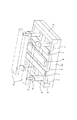
実施の形態の記憶装置の模式図を、図1及び図2に示す。図1は斜視図、図2は断面図である。
<1. Configuration of Storage Device of Embodiment>
First, the configuration of the storage device according to the embodiment of the present disclosure will be described.
1 and 2 are schematic diagrams of a storage device according to an embodiment. 1 is a perspective view, and FIG. 2 is a cross-sectional view.
図1に示すように、実施の形態の記憶装置は、互いに直交する2種類のアドレス配線(例えばワード線とビット線)の交点付近に、磁化状態で情報を保持することができるST−MRAMによる記憶素子3が配置されて成る。
即ち、シリコン基板等の半導体基体10の素子分離層2により分離された部分に、各記憶装置を選択するための選択用トランジスタを構成する、ドレイン領域8、ソース領域7、並びにゲート電極1が、それぞれ形成されている。このうち、ゲート電極1は、図中前後方向に延びる一方のアドレス配線(ワード線)を兼ねている。
As shown in FIG. 1, the storage device according to the embodiment is based on an ST-MRAM that can hold information in a magnetized state in the vicinity of an intersection of two types of address lines (for example, a word line and a bit line) orthogonal to each other. The storage element 3 is arranged.
That is, a
ドレイン領域8は、図1中左右の選択用トランジスタに共通して形成されており、このドレイン領域8には、配線9が接続されている。
そして、ソース領域7と、上方に配置された、図1中左右方向に延びるビット線6との間に、スピントルク磁化反転により磁化の向きが反転する記憶層を有する記憶素子3が配置されている。この記憶素子3は、例えば磁気トンネル接合素子(MTJ素子)により構成される。
The
A storage element 3 having a storage layer whose magnetization direction is reversed by spin torque magnetization reversal is disposed between the
図2に示すように、記憶素子3は2つの磁性層15、17を有する。この2層の磁性層15、17のうち、一方の磁性層を磁化M15の向きが固定された磁化固定層15として、他方の磁性層を磁化M17の向きが変化する磁化自由層即ち記憶層17とする。
また、記憶素子3は、ビット線6と、ソース領域7とに、それぞれ上下のコンタクト層4を介して接続されている。
これにより、2種類のアドレス配線1、6を通じて、記憶素子3に上下方向の電流を流して、スピントルク磁化反転により記憶層17の磁化M17の向きを反転させることができる。
As shown in FIG. 2, the memory element 3 has two
The storage element 3 is connected to the bit line 6 and the
As a result, a current in the vertical direction can be passed through the storage element 3 through the two types of address wirings 1 and 6, and the direction of the magnetization M17 of the
このような記憶装置では、選択トランジスタの飽和電流以下の電流で書き込みを行う必要があり、トランジスタの飽和電流は微細化に伴って低下することが知られているため、記憶装置の微細化のためには、スピントランスファの効率を改善して、記憶素子3に流す電流を低減させることが好適である。 In such a memory device, it is necessary to perform writing at a current equal to or lower than the saturation current of the selection transistor, and it is known that the saturation current of the transistor decreases with miniaturization. For this, it is preferable to improve the efficiency of the spin transfer and reduce the current flowing through the memory element 3.
また、読み出し信号を大きくするためには、大きな磁気抵抗変化率を確保する必要があり、そのためには上述のようなMTJ構造を採用すること、すなわち2層の磁性層15、17の間に中間層をトンネル絶縁層(トンネルバリア層)とした記憶素子3の構成にすることが効果的である。
このように中間層としてトンネル絶縁層を用いた場合には、トンネル絶縁層が絶縁破壊することを防ぐために、記憶素子3に流す電流量に制限が生じる。すなわち記憶素子3の繰り返し書き込みに対する信頼性の確保の観点からも、スピントルク磁化反転に必要な電流を抑制することが好ましい。なお、スピントルク磁化反転に必要な電流は、反転電流、記憶電流などと呼ばれることがある。
Further, in order to increase the read signal, it is necessary to secure a large magnetoresistance change rate. For that purpose, the above-described MTJ structure is adopted, that is, between the two
When the tunnel insulating layer is used as the intermediate layer in this way, the amount of current flowing through the memory element 3 is limited in order to prevent the tunnel insulating layer from being broken down. That is, it is preferable to suppress the current necessary for the spin torque magnetization reversal from the viewpoint of ensuring the reliability of the memory element 3 against repeated writing. Note that the current required for spin torque magnetization reversal may be referred to as reversal current or storage current.
また記憶装置は不揮発メモリ装置であるから、電流によって書き込まれた情報を安定に記憶する必要がある。つまり、記憶層の磁化の熱揺らぎに対する安定性(熱安定性)を確保する必要がある。
記憶層の熱安定性が確保されていないと、反転した磁化の向きが、熱(動作環境における温度)により再反転する場合があり、書き込みエラーとなってしまう。
本記憶装置における記憶素子3(ST−MRAM)は、従来のMRAMと比較して、スケーリングにおいて有利、すなわち体積を小さくすることは可能であるが、体積が小さくなることは、他の特性が同一であるならば、熱安定性を低下させる方向にある。
ST−MRAMの大容量化を進めた場合、記憶素子3の体積は一層小さくなるので、熱安定性の確保は重要な課題となる。
そのため、ST−MRAMにおける記憶素子3において、熱安定性は非常に重要な特性であり、体積を減少させてもこの熱安定性が確保されるように設計する必要がある。
Further, since the storage device is a nonvolatile memory device, it is necessary to stably store information written by current. That is, it is necessary to ensure the stability (thermal stability) against the thermal fluctuation of the magnetization of the storage layer.
If the thermal stability of the storage layer is not ensured, the reversed magnetization direction may be reversed again by heat (temperature in the operating environment), resulting in a write error.
The storage element 3 (ST-MRAM) in the present storage device is advantageous in scaling as compared with the conventional MRAM, that is, it is possible to reduce the volume, but the decrease in the volume has the same other characteristics. If it is, it exists in the direction which reduces thermal stability.
When the capacity of the ST-MRAM is increased, the volume of the memory element 3 is further reduced, so ensuring thermal stability becomes an important issue.
Therefore, in the storage element 3 in the ST-MRAM, thermal stability is a very important characteristic, and it is necessary to design the thermal stability to be ensured even if the volume is reduced.
<2.実施の形態の記憶素子の概要>
つぎに本開示の実施の形態の記憶素子の概要について説明する。
実施の形態の記憶素子はST−MRAMとして構成される。ST−MRAMはスピントルク磁化反転により、記憶素子の記憶層の磁化の向きを反転させて、情報の記憶を行う。
記憶層は、強磁性層を含む磁性体により構成され、情報を磁性体の磁化状態(磁化の向き)により保持するものである。
詳しくは後述するが、実施の形態の記憶素子3は、例えば図3に一例を示す層構造とされ、少なくとも2つの強磁性体層としての記憶層17、磁化固定層15を備え、またその2つの磁性層の間の中間層16を備える。
<2. Outline of Memory Element of Embodiment>
Next, an outline of the memory element according to the embodiment of the present disclosure will be described.
The storage element of the embodiment is configured as an ST-MRAM. The ST-MRAM stores information by reversing the magnetization direction of the storage layer of the storage element by spin torque magnetization reversal.
The storage layer is made of a magnetic material including a ferromagnetic layer, and holds information by the magnetization state (magnetization direction) of the magnetic material.
As will be described in detail later, the storage element 3 according to the embodiment has a layer structure as shown in FIG. 3, for example, and includes at least two
記憶層17は、膜面に垂直な磁化を有し、情報に対応して磁化の向きが変化される。
磁化固定層15は、記憶層17に記憶された情報の基準となる膜面に垂直な磁化を有する。
中間層16は、例えば非磁性体による絶縁層とされ、記憶層17と磁化固定層15の間に設けられる。
そして記憶層17、中間層16、磁化固定層15を有する層構造の積層方向にスピン偏極した電子を注入することにより、記憶層17の磁化の向きが変化して、記憶層17に対して情報の記憶が行われる。
The
The magnetization fixed
The
Then, by injecting spin-polarized electrons in the stacking direction of the layer structure including the
ここでスピントルク磁化反転について簡単に説明する。
電子は2種類のスピン角運動量をもつ。仮にこれを上向き、下向きと定義する。非磁性体内部では両者が同数であり、強磁性体内部では両者の数に差がある。記憶素子3を構成する2層の強磁性体である磁化固定層15及び記憶層17において、互いの磁気モーメントの向きが反方向状態のときに、電子を磁化固定層15から記憶層17への移動させた場合について考える。
Here, the spin torque magnetization reversal will be briefly described.
Electrons have two types of spin angular momentum. This is defined as upward and downward. The number of both is the same inside the non-magnetic material, and the number of both is different inside the ferromagnetic material. In the magnetization fixed
磁化固定層15は、高い保磁力のために磁気モーメントの向きが固定された固定磁性層である。
磁化固定層15を通過した電子はスピン偏極、すなわち上向きと下向きの数に差が生じる。非磁性層である中間層16の厚さが充分に薄く構成されていると、磁化固定層15の通過によるスピン偏極が緩和して通常の非磁性体における非偏極(上向きと下向きが同数)状態になる前に他方の磁性体、すなわち記憶層17に電子が達する。
記憶層17では、スピン偏極度の符号が逆になっていることにより、系のエネルギを下げるために一部の電子は反転、すなわちスピン角運動量の向きをかえさせられる。このとき、系の全角運動量は保存されなくてはならないため、向きを変えた電子による角運動量変化の合計と等価な反作用が記憶層17の磁気モーメントにも与えられる。
電流すなわち単位時間に通過する電子の数が少ない場合には、向きを変える電子の総数も少ないために記憶層17の磁気モーメントに発生する角運動量変化も小さいが、電流が増えると多くの角運動量変化を単位時間内に与えることができる。
The magnetization fixed
The electrons that have passed through the magnetization pinned
In the
When the current, that is, the number of electrons passing through the unit time is small, the total number of electrons changing the direction is small, and therefore the change in the angular momentum generated in the magnetic moment of the
角運動量の時間変化はトルクであり、トルクがあるしきい値を超えると記憶層17の磁気モーメントは歳差運動を開始し、その一軸異方性により180度回転したところで安定となる。すなわち反方向状態から同方向状態への反転が起こる。
磁化が同方向状態にあるとき、電流を逆に記憶層17から磁化固定層15へ電子を送る向きに流すと、今度は磁化固定層15で反射される際にスピン反転した電子が記憶層17に進入する際にトルクを与え、反方向状態へと磁気モーメントを反転させることができる。ただしこの際、反転を起こすのに必要な電流量は、反方向状態から同方向状態へと反転させる場合よりも多くなる。
The time change of the angular momentum is torque, and when the torque exceeds a certain threshold value, the magnetic moment of the
When the magnetization is in the same direction state, if a current is flowed in the opposite direction to send electrons from the
磁気モーメントの同方向状態から反方向状態への反転は直感的な理解が困難であるが、磁化固定層15が固定されているために磁気モーメントが反転できず、系全体の角運動量を保存するために記憶層17が反転する、と考えてもよい。このように、0/1の記憶は、磁化固定層15から記憶層17の方向またはその逆向きに、それぞれの極性に対応する、あるしきい値以上の電流を流すことによって行われる。
情報の読み出しは、従来型のMRAMと同様、磁気抵抗効果を用いて行われる。すなわち上述の記憶の場合と同様に膜面垂直方向に電流を流す。そして、記憶層17の磁気モーメントが、磁化固定層15の磁気モーメントに対して同方向であるか反方向であるかに従い、素子の示す電気抵抗が変化する現象を利用する。
Although it is difficult to intuitively understand the reversal of the magnetic moment from the same direction to the opposite direction, the magnetic moment cannot be reversed because the magnetization fixed
Information is read out by using the magnetoresistive effect as in the conventional MRAM. That is, a current is passed in the direction perpendicular to the film surface as in the case of the memory described above. Then, a phenomenon is used in which the electric resistance of the element changes depending on whether the magnetic moment of the
磁化固定層15と記憶層17の間の中間層16として用いる材料は金属でも絶縁体でも構わないが、より高い読み出し信号(抵抗の変化率)が得られ、かつより低い電流によって記憶が可能とされるのは、中間層として絶縁体を用いた場合である。このときの素子を強磁性トンネル接合(Magnetic Tunnel Junction:MTJ)と呼ぶ。
The material used for the
スピントルク磁化反転によって、磁性層の磁化の向きを反転させるときに、必要となる電流の閾値Icは、磁性層の磁化容易軸が面内方向であるか、垂直方向であるかによって異なる。
本実施の形態の記憶素子は垂直磁化型であるが、従前の面内磁化型の記憶素子の場合における磁性層の磁化の向きを反転させる反転電流をIc_paraとする。
同方向から逆方向(なお、同方向、逆方向とは、磁化固定層の磁化方向を基準としてみた記憶層の磁化方向)に反転させる場合、
Ic_para=(A・α・Ms・V/g(0)/P)(Hk+2πMs)
となり、逆方向から同方向に反転させる場合、
Ic_para=−(A・α・Ms・V/g(π)/P)(Hk+2πMs)
となる。
When the magnetization direction of the magnetic layer is reversed by spin torque magnetization reversal, the required current threshold Ic differs depending on whether the easy axis of magnetization of the magnetic layer is in the in-plane direction or in the vertical direction.
Although the memory element of this embodiment is a perpendicular magnetization type, the reversal current that reverses the magnetization direction of the magnetic layer in the case of a conventional in-plane magnetization type memory element is Ic_para.
When reversing from the same direction to the reverse direction (note that the same direction and the reverse direction are the magnetization directions of the storage layer with reference to the magnetization direction of the magnetization fixed layer)
Ic_para = (A · α · Ms · V / g (0) / P) (Hk + 2πMs)
And when reversing from the opposite direction to the same direction,
Ic_para = − (A · α · Ms · V / g (π) / P) (Hk + 2πMs)
It becomes.
一方、本例のような垂直磁化型の記憶素子の反転電流をIc_perpとすると、同方向から逆方向に反転させる場合、
Ic_perp=(A・α・Ms・V/g(0)/P)(Hk−4πMs)
となり、逆方向から同方向に反転させる場合、
Ic_perp=−(A・α・Ms・V/g(π)/P)(Hk−4πMs)
となる。
On the other hand, when the reversal current of the perpendicular magnetization type storage element as in this example is Ic_perp, when reversing from the same direction to the reverse direction,
Ic_perp = (A · α · Ms · V / g (0) / P) (Hk−4πMs)
And when reversing from the opposite direction to the same direction,
Ic_perp = − (A · α · Ms · V / g (π) / P) (Hk−4πMs)
It becomes.
ただし、Aは定数、αはダンピング定数、Msは飽和磁化、Vは素子体積、Pはスピン分極率、g(0)、g(π)はそれぞれ同方向時、逆方向時にスピントルクが相手の磁性層に伝達される効率に対応する係数、Hkは磁気異方性である。 Where A is a constant, α is a damping constant, Ms is saturation magnetization, V is element volume, P is spin polarizability, g (0) and g (π) are in the same direction and spin torque in the opposite direction. A coefficient Hk corresponding to the efficiency transmitted to the magnetic layer is magnetic anisotropy.
上記各式において、垂直磁化型の場合の(Hk−4πMs)と面内磁化型の場合の(Hk+2πMs)とを比較すると、垂直磁化型が低記憶電流化により適していることが理解できる。 In each of the above formulas, comparing (Hk−4πMs) in the perpendicular magnetization type and (Hk + 2πMs) in the in-plane magnetization type, it can be understood that the perpendicular magnetization type is more suitable for reducing the storage current.
垂直異方性を有する磁性材料にとしてCo−Fe−B合金等があり、ST−MRAMにおいて大きな読み出し信号を与える高磁気抵抗変化率を実現するために、トンネル障壁(中間層16)としてのMgOと組み合わせが可能な点で有望である。
しかしながら、垂直磁気異方性の起源として酸化物との界面異方性を持つ本構成では、他の垂直磁化材料に比べ低い垂直異方性エネルギーによる低い保持特性(熱安定性)が懸念されている。
保持特性を向上させるためには磁性層の体積を増やすなどの方法があるが、膜厚が増加することで低下する界面異方性とのトレードオフとなり好ましくない。
As a magnetic material having perpendicular anisotropy, there is a Co—Fe—B alloy or the like, and MgO as a tunnel barrier (intermediate layer 16) is used in order to realize a high magnetoresistance change rate that gives a large read signal in ST-MRAM. It is promising in that it can be combined with.
However, in this configuration, which has interface anisotropy with oxide as the origin of perpendicular magnetic anisotropy, there is concern about low retention characteristics (thermal stability) due to low perpendicular anisotropy energy compared to other perpendicular magnetization materials. Yes.
In order to improve the retention characteristics, there is a method of increasing the volume of the magnetic layer, but this is not preferable because it is a trade-off with the interface anisotropy that decreases as the film thickness increases.
メモリとして存在し得るためには、書き込まれた情報を保持することができなければならない。
情報を保持する能力の指標として、熱安定性の指標Δ(=KV/kBT)の値で判断される。このΔは、下記式により表される。
Δ=KV/kBT=Ms・V・Hk・(1/2kB・T)
In order to be able to exist as a memory, it must be able to hold the written information.
As an index of the ability to hold information, it is determined by the value of the thermal stability index Δ (= KV / k B T). This Δ is represented by the following equation.
Δ = KV / k B T = Ms · V · Hk · (1/2 kB · T)
ここで、Hk:実効的な異方性磁界、kB:ボルツマン定数、T:絶対温度、Ms:飽和磁化量、V:記憶層17の体積、K:異方性エネルギーである。
実効的な異方性磁界Hkには、形状磁気異方性、誘導磁気異方性、結晶磁気異方性等の影響が取り込まれており、単磁区の一斉回転モデルを仮定した場合、これは保磁力と同等となる。
Here, Hk: effective anisotropy magnetic field, k B : Boltzmann constant, T: absolute temperature, Ms: saturation magnetization, V: volume of
The effect of shape magnetic anisotropy, induced magnetic anisotropy, crystal magnetic anisotropy, etc. is incorporated into the effective anisotropy magnetic field Hk. Equivalent to coercive force.
<3.実施の形態の具体的構成>
続いて、本開示の実施の形態の具体的構成について説明する。
記憶装置の構成は先に図1で述べたとおり、直交する2種類のアドレス配線1,6(例えばワード線とビット線)の交点付近に、磁化状態で情報を保持することができる記憶素子3が配置されるものである。
そして2種類のアドレス配線1、6を通じて、記憶素子3に上下方向の電流を流して、スピントルク磁化反転により記憶層17の磁化の向きを反転させることができる。
<3. Specific Configuration of Embodiment>
Subsequently, a specific configuration of the embodiment of the present disclosure will be described.
As described above with reference to FIG. 1, the configuration of the storage device is a storage element 3 capable of holding information in a magnetized state near the intersection of two kinds of orthogonal address lines 1 and 6 (for example, a word line and a bit line). Is arranged.
The direction of magnetization of the
図3は実施の形態の記憶素子3(ST−MRAM)の層構造の例を表している。
記憶素子3は、下地層14、磁化固定層15、中間層16、記憶層17、酸化物キャップ層18、キャップ保護層19を有する。
FIG. 3 illustrates an example of a layer structure of the memory element 3 (ST-MRAM) according to the embodiment.
The storage element 3 includes a
この図3の例のように、記憶素子3は、スピントルク磁化反転により磁化M17の向きが反転する記憶層17に対して、下層に磁化固定層15を設けている。
ST−MRAMにおいては、記録層17の磁化M17と磁化固定層15の磁化M15の相対的な角度によって情報の0、1を規定している。
As in the example of FIG. 3, the storage element 3 is provided with a magnetization fixed
In the ST-MRAM, 0 or 1 of information is defined by the relative angle between the magnetization M17 of the
記憶層17は、磁化の方向が層面垂直方向に自由に変化する磁気モーメントを有する強磁性体から構成されている。磁化固定層15は、磁化が膜面垂直方向に固定された磁気モーメントを有する強磁性体から構成されている。
情報の記憶は一軸異方性を有する記憶層17の磁化の向きにより行う。書込みは、膜面垂直方向に電流を印加し、スピントルク磁化反転を起こすことにより行う。このように、スピン注入により磁化の向きが反転する記憶層に対して、下層に磁化固定層15が設けられ、記憶層17の記憶情報(磁化方向)の基準とされる。
The
Information is stored according to the magnetization direction of the
記憶層17と磁化固定層15との間には、トンネルバリア層(トンネル絶縁層)となる中間層16が設けられ、記憶層17と磁化固定層15とにより、MTJ素子が構成されている。
An
また、磁化固定層15の下には下地層14が形成されている。
記憶層17の上(つまり記憶層17から見て中間層16とは反対側)には酸化物キャップ層18が形成されている。
さらに酸化物キャップ層18の上(つまり保磁力強化層18からみて記憶層17とは反対側)にキャップ保護層19が形成されている。
An
An
Further, a
本実施の形態では、記憶層17及び磁化固定層15としてはCo−Fe−Bを用いる。
なお、記憶層17及び磁化固定層15を構成する磁性体はCo−Fe−B合金に限らず、Co−Fe−C合金、Ni−Fe−B合金、Ni−Fe−C合金でも良い。
磁化固定層15は情報の基準であるので、記録や読み出しによって磁化の方向が変化してはいけないが、必ずしも特定の方向に固定されている必要はなく、記憶層17よりも保磁力を大きくするか、膜厚を厚くするか、あるいは磁気ダンピング定数を大きくして記憶層17よりも動きにくくすればよい。
In the present embodiment, Co—Fe—B is used for the
The magnetic material constituting the
Since the magnetization fixed
中間層16(トンネルバリア層)は例えばMgOとする。MgO(酸化マグネシウム)層とした場合には、磁気抵抗変化率(MR比)を高くすることができる。このようにMR比を高くすることによって、スピン注入の効率を向上して、記憶層17の磁化M17の向きを反転させるために必要な電流密度を低減することができる。
なお中間層16は、酸化マグネシウムから成る構成とする他にも、例えば酸化アルミニウム、窒化アルミニウム、SiO2、Bi2O3、MgF2、CaF、SrTiO2、AlLaO3、Al−N−O等の各種の絶縁体、誘電体、半導体を用いて構成することもできる。
The intermediate layer 16 (tunnel barrier layer) is, for example, MgO. When the MgO (magnesium oxide) layer is used, the magnetoresistance change rate (MR ratio) can be increased. By increasing the MR ratio in this way, the efficiency of spin injection can be improved and the current density required to reverse the direction of the magnetization M17 of the
In addition to the structure made of magnesium oxide, the
下地層14およびキャップ保護層19としては、Ta、Ti、W、Ru等各種金属およびTiN等の導電性窒化物を用いることができる。また、下地層14および保護層20は単層で用いても良いし、異なる材料を複数積層しても良い。
As the
酸化物キャップ層18は、この例では第1キャップ層18a、第2キャップ層18bの2層の積層構造とされている。
第1キャップ層18a、第2キャップ層18bのそれぞれは、酸化ケイ素、酸化マグネシウム、酸化タンタル、酸化アルミニウム、酸化コバルト、フェライト、酸化チタン、酸化クロム、チタン酸ストロンチウム、酸化アルミニウムランタン、酸化亜鉛による層、もしくはこれらの酸化物の混合物による層として形成することが好ましい。
また、記憶層17に隣接する側である第1キャップ層18aは、酸化マグネシウムの層とすることが好ましい。
なお、図3の例では第1キャップ層18a、第2キャップ層18bの2層の積層構造としたが、3層以上の酸化物層の積層構造としてもよい。
In this example, the
Each of the
The
In the example of FIG. 3, a two-layered structure of the
本実施の形態においては、特に、記憶層17が受ける実効的な反磁界の大きさが記憶層17の飽和磁化量Msよりも小さくなるように、記憶層17の組成が調整されている。
前述したように、記憶層17の強磁性材料Co−Fe−B組成を選定し、記憶層17が受ける実効的な反磁界の大きさを低くして、記憶層の飽和磁化量Msよりも小さくなるようにする。これにより記憶層17の磁化は膜面垂直方向を向く。
さらに、本実施の形態において、中間層16である絶縁層を、酸化マグネシウム層(MgO)とした場合には、磁気抵抗変化率(MR比)を高くすることができる。このようにMR比を高くすることによって、スピン注入の効率を向上して、記憶層17の磁化の向きを反転させるために必要な電流密度を低減することができる。
In the present embodiment, in particular, the composition of the
As described above, the composition of the ferromagnetic material Co—Fe—B of the
Furthermore, in this embodiment, when the insulating layer that is the
記憶素子3の記憶層17が、記憶層17が受ける実効的な反磁界の大きさが記憶層17の飽和磁化量Msよりも小さくなるように構成されているので、記憶層が受ける反磁界が低くなっており、記憶層の磁化の向きを反転させるために必要となる、書き込み電流量を低減することができる。これは垂直磁気異方性を記憶層17がもつために垂直磁化型ST−MRAMの反転電流が適用でき、反磁界の点で有利になるためである。
一方、記憶層17の飽和磁化量Msを低減しなくても書き込み電流量を低減することができるため、記憶層17の飽和磁化量Msを充分な量として、記憶層17の熱安定性を確保することが可能になる。
Since the
On the other hand, since the amount of write current can be reduced without reducing the saturation magnetization amount Ms of the
さらに本実施の形態では、記憶層17に接する2層の酸化物層による酸化物キャップ層18を設けている。
酸化物積層構造である酸化物キャップ層18を設けることで、垂直磁気異方性を調整することができ、単層の酸化物を用いた構成よりも記憶層17の保磁力及び情報保持特性(熱安定性指標Δ)を増大させることができる。
これにより特性バランスに優れた記憶素子を構成することができる。
Further, in the present embodiment, the
By providing the
As a result, a memory element with excellent characteristic balance can be configured.
本実施の形態の記憶素子3は、下地層14からキャップ保護層19までの各層を真空装置内で順次連続的に成膜して積層構造を形成する。その後エッチング等の加工により記憶素子3のパターンを形成することにより、製造することができる。
In the memory element 3 of the present embodiment, each layer from the
なお、磁化固定層15は、単層の強磁性層から成る構成、或いは複数層の強磁性層を、非磁性層を介して積層した、積層フェリピン構造とすることが出来る。
積層フェリピン構造の磁化固定層15を構成する強磁性層の材料としては、Co,CoFe,CoFeB等を用いることができる。また、非磁性層の材料としては、Ru,Re,Ir,Os等を用いることができる。
或いは反強磁性層と強磁性層の反強磁性結合を利用することにより、その磁化の向きが固定された構成とすることができる。
反強磁性層の材料としては、FeMn合金、PtMn合金、PtCrMn合金、NiMn合金、IrMn合金、NiO、Fe2O3等の磁性体を挙げることができる。
また、これらの磁性体に、Ag,Cu,Au,Al,Si,Bi,Ta,B,C,O,N,Pd,Pt,Zr,Hf,Ir,W,Mo,Nb等の非磁性元素を添加して、磁気特性を調整したり、その他の結晶構造や結晶性や物質の安定性等の各種物性を調整したりすることができる。
磁化固定層15を積層フェリピン構造とすれば、磁化固定層15を外部磁界に対して鈍化させ、磁化固定層15に起因する漏洩磁界を遮断するとともに複数の磁性層の層間結合による、磁化固定層15の垂直磁気異方性の強化を図ることが出来る。
Note that the magnetization fixed
Co, CoFe, CoFeB, or the like can be used as the material of the ferromagnetic layer constituting the magnetization fixed
Alternatively, the magnetization direction can be fixed by using antiferromagnetic coupling between the antiferromagnetic layer and the ferromagnetic layer.
Examples of the material of the antiferromagnetic layer include magnetic materials such as FeMn alloy, PtMn alloy, PtCrMn alloy, NiMn alloy, IrMn alloy, NiO, and Fe 2 O 3 .
In addition, nonmagnetic elements such as Ag, Cu, Au, Al, Si, Bi, Ta, B, C, O, N, Pd, Pt, Zr, Hf, Ir, W, Mo, and Nb are included in these magnetic materials. Can be added to adjust the magnetic properties and other physical properties such as crystal structure, crystallinity and material stability.
If the magnetization pinned
<4.実施の形態に関する実験>
[実験1]
本実験は、図3のように記憶素子3に酸化物の積層構造とした酸化物キャップ層18を設けた場合の磁気特性を評価したものである。磁化曲線の測定を行い、保磁力Hcを測定した。
試料は、試料1〜試料8の8種類を用意した。試料2〜試料8が実施の形態の記憶素子3に相当するものであり、試料1が比較例となる比較用の試料である。
<4. Experiments on Embodiments>
[Experiment 1]
In this experiment, the magnetic characteristics in the case where an
Eight types of samples, Sample 1 to
各試料の層構造を図4に示す。
酸化物キャップ層18以外は試料1〜試料8で同様であり、図4Aに示す。
・下地層14:膜厚15nmのTa膜と、膜厚10nmのRu膜の積層膜
・磁化固定層15:膜厚2nmのCo−Pt層と、膜厚0.7nmのRu膜と、膜厚1.2nmの[Co20Fe80]70B30膜の積層膜
・中間層16(トンネル絶縁層):膜厚1nmの酸化マグネシウム膜
・記憶層17:膜厚2nmの[Co20Fe80]70B30膜
The layer structure of each sample is shown in FIG.
Samples 1 to 8 are the same except for the
-Underlayer 14: Laminated film of Ta film with a thickness of 15 nm and Ru film with a thickness of 10 nm-Magnetization fixed layer 15: Co-Pt layer with a thickness of 2 nm, Ru film with a thickness of 0.7 nm, and film thickness Stacked film of 1.2 nm [Co 20 Fe 80 ] 70 B 30 film / intermediate layer 16 (tunnel insulating layer): magnesium oxide film with a thickness of 1 nm / memory layer 17: [Co 20 Fe 80 ] 70 with a thickness of 2 nm B 30 membrane
記憶層17に隣接する酸化物キャップ層18の構造を図4Bに示している。
・試料1(比較例):膜厚0.9nmの酸化マグネシウム
・試料2:膜厚0.5nmの酸化マグネシウムと膜厚0.4nmの酸化アルミニウム
・試料3:膜厚0.5nmの酸化マグネシウムと膜厚1.0nmの酸化タンタル
・試料4:膜厚0.5nmの酸化マグネシウムと膜厚1.0nmの酸化クロム
・試料5:膜厚0.4nmの酸化アルミニウムと膜厚0.5nmの酸化マグネシウム
・試料6:膜厚1.0nmの酸化タンタルと膜厚0.5nmの酸化マグネシウム
・試料7:膜厚1.0nmの酸化クロムと膜厚0.5nmの酸化マグネシウム
・試料8:膜厚0.5nmの酸化アルミニウムと膜厚0.5nmの酸化タンタル
The structure of the
Sample 1 (comparative example): magnesium oxide with a thickness of 0.9 nm Sample 2: magnesium oxide with a thickness of 0.5 nm and aluminum oxide with a thickness of 0.4 nm Sample 3: magnesium oxide with a thickness of 0.5 nm Tantalum oxide with a film thickness of 1.0 nm. Sample 4: Magnesium oxide with a film thickness of 0.5 nm and chromium oxide with a film thickness of 1.0 nm. Sample 5: Aluminum oxide with a film thickness of 0.4 nm and magnesium oxide with a film thickness of 0.5 nm. Sample 6: Tantalum oxide with a thickness of 1.0 nm and magnesium oxide with a thickness of 0.5 nm Sample 7: Chromium oxide with a thickness of 1.0 nm and magnesium oxide with a thickness of 0.5 nm Sample 8: Thickness of 0. 5nm aluminum oxide and 0.5nm thick tantalum oxide
尚、各試料の酸化物キャップ層18の上部には、キャップ保護層19(Ta,Ru,W等)を積層させている
A cap protective layer 19 (Ta, Ru, W, etc.) is laminated on the
試料2〜試料4は、記憶層17に接する第1キャップ層18aに酸化マグネシウムを用いたものとした。
試料5〜試料7は、記憶層17に接しない第2キャップ層18aに酸化マグネシウムを用い、第1キャップ層18aは酸化マグネシウム以外とした。
試料8は、第1キャップ層18a,第2キャップ層18bとも、酸化マグネシウム以外としたものである。
In
In Samples 5 to 7, magnesium oxide was used for the
In the
各試料は、厚さ0.725mmのシリコン基板上に、厚さ300nmの熱酸化膜を形成し、その上に上記の構成の記憶素子を形成した。
また下地層とシリコン基板との間に図示しない膜厚100nmのCu膜を設けた。
中間層16以外の各層は、DCマグネトロンスパッタ法を用いて成膜した。酸化物を用いた中間層16は、RFマグネトロンスパッタ法もしくは、DCマグネトロンスパッタ法を用いて金属層を成膜した後酸化チャンバーで酸化した。
記憶素子を構成する各層を成膜した後に、磁場中熱処理炉で、300℃・1時間の熱処理を行った。
In each sample, a 300 nm thick thermal oxide film was formed on a 0.725 mm thick silicon substrate, and a memory element having the above-described structure was formed thereon.
A Cu film with a thickness of 100 nm (not shown) was provided between the base layer and the silicon substrate.
Each layer other than the
After forming each layer constituting the memory element, heat treatment was performed at 300 ° C. for 1 hour in a heat treatment furnace in a magnetic field.
(磁化曲線の測定)
各試料としての記憶素子の磁化曲線を、磁気カー効果測定によって、測定した。
このとき、測定には微細加工後の素子ではなく、ウェハ上に磁化曲線評価用に特別に設けた8mm×8mm程度のバルクフィルム部分を用いた。また測定磁界は、膜面垂直方向に印加した。
(Measurement of magnetization curve)
The magnetization curve of the memory element as each sample was measured by magnetic Kerr effect measurement.
At this time, not the element after microfabrication but a bulk film portion of about 8 mm × 8 mm specially provided for evaluating the magnetization curve on the wafer was used for the measurement. The measurement magnetic field was applied in the direction perpendicular to the film surface.
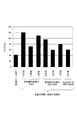
図5は、試料1〜試料8について磁化曲線から求められる保磁力Hcを示したものである。
キャップ層の磁化曲線の形状は、いずれの構成においても磁化曲線は良好な角型を示し、記憶層17であるのCo−Fe−B合金が界面異方性によって垂直磁気異方性を十分に発現している。
キャップ層が2層の酸化物の積層構造である試料2〜試料8においては、比較例(試料1)のような単層の酸化物を用いた構成よりも保磁力の値が増え、最大で2倍程度に増大している。
FIG. 5 shows the coercive force Hc obtained from the magnetization curves for Sample 1 to
As for the shape of the magnetization curve of the cap layer, the magnetization curve shows a good square shape in any configuration, and the Co—Fe—B alloy as the
In
これは、記憶層17/酸化物キャップ18間の歪の影響が緩和したためと考えられる。実際の材料においては、熱処理に伴って結晶化したCo−Fe−B合金と酸化マグネシウムによる中間層16のように、高配向な磁性層/酸化物界面には局所的な歪が導入されており、磁気特性を劣化させている。
特にCoFe系磁性膜と酸化マグネシウム膜の間には、格子定数のミスマッチが大きく、歪による影響が大きいことが知られている。
試料2〜試料8では、酸化マグネシウム単体のキャップ層に対しミスマッチの異なる酸化物を組み合わせて積層させることによって、歪が変調・補償され、磁気特性が改善されていると考えられる。
This is presumably because the influence of strain between the
In particular, it is known that there is a large lattice constant mismatch between the CoFe-based magnetic film and the magnesium oxide film, and the influence of strain is large.
In
加えて試料2〜試料8では、格子定数の異なる酸化物が積層構造をとることによって、積層上部もしくは下部いずれかに膜面内方向の圧縮歪が生じ、キャップ保護層19として積層しているRuやW、Ta層の熱処理による酸化物への拡散が抑制されていると考えられる。
結果、拡散したキャップ保護層19と酸化物が混ざることによって起きる界面異方性の劣化を防ぐ効果が歪の補償効果と同時に得られている。
In addition, in
As a result, the effect of preventing the deterioration of the interface anisotropy caused by mixing of the diffused cap
なお、垂直磁気異方性を調整するために積層する酸化物は3層以上でもよい。また各試料で示した酸化物に加えて、酸化ケイ素、酸化コバルト、フェライト、酸化チタン、チタン酸ストロンチウム、酸化アルミニウムランタン、酸化亜鉛、もしくはこれらの酸化物の混合層を含むものでも良い。 Note that three or more oxides may be stacked to adjust the perpendicular magnetic anisotropy. Further, in addition to the oxides shown in each sample, silicon oxide, cobalt oxide, ferrite, titanium oxide, strontium titanate, aluminum lanthanum oxide, zinc oxide, or a mixed layer of these oxides may be included.
試料2,3,4と、試料5,6,7を比較すると、酸化マグネシウムが記憶層17との界面にある構成の方が、無い構成に比べ1.2倍程度の保磁力を持つ。
このことから磁性層との界面異方性を効果的に発現できる酸化マグネシウムが界面側で或る第1キャップ層18aとされることが好ましい。但し記憶層17に隣接している酸化物は酸化マグネシウム以外でも単層酸化物の場合(試料1)に比較して保磁力を増強する効果は得られている。
Comparing
Therefore, it is preferable that magnesium oxide capable of effectively expressing the interface anisotropy with the magnetic layer be the
また、実験ではCo−Fe−B合金のB組成を30%としたが、TMR値や耐熱性の観点からB組成を20〜40%程度と変化させても良い。
記憶層17を構成する磁性体はCo−Fe−B合金に限らず、Co−Fe−C合金、 Ni−Fe−B合金、Ni−Fe−C合金でも良い。
記憶層17および磁化固定層15のCo−Fe−B合金に非磁性元素を添加することも有効であり、この場合の非磁性層の材料としては、Ru,Os,Re,Ir,Au,Ag,Cu,Al,Bi,Si,B,C,Cr,Ta,Pd,Pt,Zr,Hf,W,Mo,Nbまたはそれらの合金を用いて、磁気特性を調整することができる。
In the experiment, the B composition of the Co—Fe—B alloy was set to 30%, but the B composition may be changed to about 20 to 40% from the viewpoint of TMR value and heat resistance.
The magnetic body constituting the
It is also effective to add a nonmagnetic element to the Co—Fe—B alloy of the
[実験2]
本実験は、図3の記憶素子3に積層構造の酸化物キャップ層18を設けた場合の特性を調べたものである。磁気抵抗曲線の測定、反転電流値からの熱安定性測定を行った。試料は、試料9〜試料11の3種類を用意した。試料10、試料11が実施の形態の記憶素子3に相当するものであり、試料9は比較用の試料である。
[Experiment 2]
In this experiment, characteristics in the case where the
各試料の層構造を図4に示す。
酸化物キャップ層18以外は試料9〜試料11で同様であり、図6Aに示す。
・下地層14:膜厚15nmのTa膜と、膜厚10nmのRu膜の積層膜
・磁化固定層15:膜厚2nmのCo−Pt層と、膜厚0.7nmのRu膜と、膜厚1.2nmの[Co20Fe80]70B30膜の積層膜
・中間層16(トンネル絶縁層):膜厚1nmの酸化マグネシウム膜
・記憶層17:膜厚2nmの[Co20Fe80]70B30膜
The layer structure of each sample is shown in FIG.
-Underlayer 14: Laminated film of Ta film with a thickness of 15 nm and Ru film with a thickness of 10 nm-Magnetization fixed layer 15: Co-Pt layer with a thickness of 2 nm, Ru film with a thickness of 0.7 nm, and film thickness Stacked film of 1.2 nm [Co 20 Fe 80 ] 70 B 30 film / intermediate layer 16 (tunnel insulating layer): magnesium oxide film with a thickness of 1 nm / memory layer 17: [Co 20 Fe 80 ] 70 with a thickness of 2 nm B 30 membrane
記憶層17に隣接する酸化物キャップ層18の構造を図6Bに示している。
・試料9(比較例):膜厚0.9nmの酸化マグネシウム
・試料10:膜厚0.5nmの酸化マグネシウムと膜厚0.4nmの酸化アルミニウム
・試料11:膜厚0.5nmの酸化マグネシウムと膜厚1.0nmの酸化クロム
The structure of the
Sample 9 (comparative example): Magnesium oxide with a thickness of 0.9 nm Sample 10: Magnesium oxide with a thickness of 0.5 nm and aluminum oxide with a thickness of 0.4 nm Sample 11: Magnesium oxide with a thickness of 0.5 nm 1.0nm thick chromium oxide
いずれの構成も、酸化物キャップ層18の上部に膜厚5nmのRuと膜厚3nmのTaによるキャップ保護層19が形成されている。
In either configuration, a cap
各試料は、厚さ0.725mmのシリコン基板上に、厚さ300nmの熱酸化膜を形成し、その上に上記の構成の記憶素子を形成した。また下地層とシリコン基板との間に図示しない膜厚100nmのCu膜(後述するワード線となるもの)を設けた。
中間層16以外の各層は、DCマグネトロンスパッタ法を用いて成膜した。酸化物を用いた中間層16は、RFマグネトロンスパッタ法もしくは、DCマグネトロンスパッタ法を用いて金属層を成膜した後酸化チャンバーで酸化した。
さらに、記憶素子を構成する各層を成膜した後に、磁場中熱処理炉で、300℃・1時間の熱処理を行った。
In each sample, a 300 nm thick thermal oxide film was formed on a 0.725 mm thick silicon substrate, and a memory element having the above-described structure was formed thereon. A Cu film (not shown) having a thickness of 100 nm (to be described later) was provided between the base layer and the silicon substrate.
Each layer other than the
Further, after forming each layer constituting the memory element, heat treatment was performed at 300 ° C. for 1 hour in a heat treatment furnace in a magnetic field.
次に、ワード線部分をフォトリソグラフィによってマスクした後に、ワード線以外の部分の積層膜に対してArプラズマにより選択エッチングを行うことにより、ワード線(下部電極)を形成した。
この際に、ワード線部分以外は、基板の深さ5nmまでエッチングされた。その後、電子ビーム描画装置により記憶素子のパターンのマスクを形成し、積層膜に対して選択エッチングを行い、記憶素子を形成した。
記憶素子部分以外は、ワード線のCu層直上までエッチングした。
Next, after masking the word line portion by photolithography, the word line (lower electrode) was formed by performing selective etching with Ar plasma on the laminated film other than the word line.
At this time, except for the word line portion, the substrate was etched to a depth of 5 nm. Thereafter, a mask of a memory element pattern was formed by an electron beam drawing apparatus, and selective etching was performed on the laminated film to form a memory element.
Except for the memory element portion, the etching was performed up to the Cu layer of the word line.
なお、特性評価用の記憶素子には、磁化反転に必要なスピントルクを発生させるために、記憶素子に充分な電流を流す必要があるため、中間層16(トンネル絶縁層)の抵抗値を抑える必要がある。
そこで、記憶素子のパターンを、短軸0.07μm×長軸0.07μmの円形状として、記憶素子の面積抵抗値(Ωμm2)が20Ωμm2となるようにした。
次に、記憶素子部分以外を、厚さ100nm程度のAl2O3のスパッタリングによって絶縁した。その後、フォトリソグラフィを用いて、上部電極となるビット線及び測定用のパッドを形成した。
このようにして、記憶素子3に相当する各試料を作製した。
In addition, since it is necessary to flow a sufficient current through the memory element in order to generate a spin torque necessary for magnetization reversal, the resistance value of the intermediate layer 16 (tunnel insulating layer) is suppressed. There is a need.
Therefore, the memory element pattern is a circular shape having a minor axis of 0.07 μm and a major axis of 0.07 μm, and the area resistance value (Ωμm 2 ) of the memory element is 20 Ωμm 2 .
Next, the portions other than the memory element portion were insulated by sputtering of Al 2 O 3 having a thickness of about 100 nm. Thereafter, a bit line to be an upper electrode and a measurement pad were formed using photolithography.
In this way, each sample corresponding to the memory element 3 was produced.
作製した記憶素子の各試料9〜試料11に対して、それぞれ以下のようにして、特性の評価を行った。測定に先立ち、反転電流のプラス方向とマイナス方向の値を対称になるように制御することを可能にするため、記憶素子に対して、外部から磁界を与えることができるように構成した。また、記憶素子に印加される電圧が、絶縁層が破壊しない範囲内の1Vまでとなるように設定した。
The characteristics of each of the produced
(磁気抵抗曲線の測定(TMR測定))
記憶素子の磁気抵抗曲線を磁場を印加しながら、素子抵抗を測定することで評価した。
(Magnetic resistance curve measurement (TMR measurement))
The magnetoresistance curve of the memory element was evaluated by measuring the element resistance while applying a magnetic field.
(反転電流値及び熱安定性の測定)
実施の形態の記憶素子3の書き込み特性を評価する目的で、反転電流値の測定を行った。記憶素子に10μsから100msのパルス幅の電流を流して、その後の記憶素子の抵抗値を測定した。
さらに、記憶素子に流す電流量を変化させて、この記憶素子の記憶層の磁化の向きが反転する電流値を求めた。
(Measurement of reversal current value and thermal stability)
For the purpose of evaluating the writing characteristics of the memory element 3 of the embodiment, the inversion current value was measured. A current having a pulse width of 10 μs to 100 ms was passed through the memory element, and then the resistance value of the memory element was measured.
Furthermore, the amount of current flowing through the storage element was changed to obtain a current value at which the magnetization direction of the storage layer of the storage element was reversed.
また、記憶素子の磁気抵抗曲線を複数回測定することによって得られる保磁力Hcの分散が記憶素子の前述した保持特性(熱安定性)の指標(Δ)に対応する。
測定される保磁力Hcの分散が少ないほど高いΔ値を持つ。
そして、記憶素子間のばらつきを考慮するために、同一構成の記憶素子を各々20個程度作製して、上述の測定を行い、反転電流値及び熱安定性の指標Δの平均値を求めた。
Further, the dispersion of the coercive force Hc obtained by measuring the magnetoresistive curve of the memory element a plurality of times corresponds to the above-described index (Δ) of the retention characteristic (thermal stability) of the memory element.
The smaller the dispersion of the measured coercive force Hc, the higher the Δ value.
Then, in order to take into account the variation between the memory elements, about 20 memory elements having the same configuration were manufactured, and the above-described measurement was performed to obtain the average value of the inversion current value and the thermal stability index Δ.
図7には、試料9〜試料11の磁気抵抗曲線および電流による書き込みでの磁化反転特性の評価をまとめた。
TMR(トンネル磁気抵抗効果)値、保磁力Hc、熱安定性指標Δ、反転電流密度JcOを示している。
試料10,試料11では、実験1のバルクフィルムにおける比較を反映しており、TMR(トンネル磁気抵抗効果)値や反転電流密度を比較例(試料9)と同程度に保ちながら、保磁力Hcと保持特性値(熱安定性指標Δ)が1.1〜1.4倍に上昇していることがわかる。
このことから、酸化物キャップ層18を積層構造とすることの優位性が確認された。
FIG. 7 summarizes the magnetic resistance curves of
TMR (tunnel magnetoresistance effect) value, coercive force Hc, thermal stability index Δ, and inversion current density JcO are shown.
From this, the superiority of the
なお、試料10,試料11の構成に限らず、実験1で挙げたように効果のある範囲で酸化物キャップ層の積層構造を変化させてもよい。
また酸化物キャップ層18と接するキャップ保護層19をRu以外に変えることによって反転電流を下げるような構成としてもよい。
In addition, not only the configurations of the
Further, the
以上の実験1,実験2からもわかるように、本実施の形態の記憶素子3は、垂直磁化型のMTJおよびこれを用いた大容量、低消費電力なST−MRAM記憶素子、記憶装置の製造を容易にする効果を有する。
As can be seen from Experiment 1 and
なお本技術は以下のような構成も採ることができる。
(1) 膜面に対して垂直な磁化を有し、情報を磁性体の磁化状態により保持する記憶層と、
上記記憶層に記憶された情報の基準となる、膜面に対して垂直な磁化を有する磁化固定層と、
上記記憶層と上記磁化固定層の間に設けられる非磁性体による中間層と、
上記記憶層に隣接し、上記中間層と反対側に設けられる、2層以上の酸化物で形成されたキャップ層と、
を有し、
上記記憶層、上記中間層、上記磁化固定層を有する層構造の積層方向に流れる電流に伴って発生するスピントルク磁化反転を利用して上記記憶層の磁化を反転させることにより情報の記憶を行う記憶素子。
(2)上記キャップ層は、酸化ケイ素、酸化マグネシウム、酸化タンタル、酸化アルミニウム、酸化コバルト、フェライト、酸化チタン、酸化クロム、チタン酸ストロンチウム、酸化アルミニウムランタン、酸化亜鉛による層、もしくはこれらの酸化物の混合物による層のいずれかを含む上記(1)に記載の記憶素子。
(3)2層以上で形成される上記キャップ層において、上記記憶層に隣接する層は、酸化マグネシウムの層である上記(1)又は(2)に記載の記憶素子。
(4)上記記憶層を構成する強磁性層材料がCo−Fe−Bである上記(1)乃至(3)のいずれかに記載の記憶素子。
In addition, this technique can also take the following structures.
(1) a storage layer having magnetization perpendicular to the film surface and holding information by the magnetization state of the magnetic material;
A magnetization fixed layer having a magnetization perpendicular to the film surface, which serves as a reference for information stored in the storage layer;
A nonmagnetic intermediate layer provided between the storage layer and the magnetization fixed layer;
A cap layer formed of two or more oxide layers provided adjacent to the memory layer and on the opposite side of the intermediate layer;
Have
Information is stored by reversing the magnetization of the storage layer by utilizing the spin torque magnetization reversal that occurs with the current flowing in the stacking direction of the layer structure having the storage layer, the intermediate layer, and the magnetization fixed layer. Memory element.
(2) The cap layer is composed of silicon oxide, magnesium oxide, tantalum oxide, aluminum oxide, cobalt oxide, ferrite, titanium oxide, chromium oxide, strontium titanate, aluminum lanthanum oxide, zinc oxide, or a layer of these oxides. The memory element according to (1), including any one of layers made of a mixture.
(3) The memory element according to (1) or (2), wherein in the cap layer formed of two or more layers, the layer adjacent to the memory layer is a layer of magnesium oxide.
(4) The memory element according to any one of (1) to (3), wherein the ferromagnetic layer material constituting the memory layer is Co—Fe—B.
1 ゲート電極、2 素子分離層、3 記憶素子、4 コンタクト層、6 ビット線、7 ソース領域、8 ドレイン領域、9 配線、10 半導体基体、14 下地層、15 磁化固定層、16 中間層、17 記憶層、18 酸化物キャップ層、19 キャップ保護層 DESCRIPTION OF SYMBOLS 1 Gate electrode, 2 Element separation layer, 3 Memory element, 4 Contact layer, 6 Bit line, 7 Source region, 8 Drain region, 9 Wiring, 10 Semiconductor substrate, 14 Underlayer, 15 Magnetization fixed layer, 16 Intermediate layer, 17 Memory layer, 18 oxide cap layer, 19 cap protective layer
Claims (4)
上記記憶層に記憶された情報の基準となる、膜面に対して垂直な磁化を有する磁化固定層と、
上記記憶層と上記磁化固定層の間に設けられる非磁性体による中間層と、
上記記憶層に隣接し、上記中間層と反対側に設けられる、酸化マグネシウム及び酸化アルミニウムの2層の酸化物あるいは酸化マグネシウム及び酸化クロムの2層の酸化物のいずれかで形成されたキャップ層と、
を有し、
上記記憶層、上記中間層、上記磁化固定層を有する層構造の積層方向に流れる電流に伴って発生するスピントルク磁化反転を利用して上記記憶層の磁化を反転させることにより情報の記憶を行う記憶素子。 A storage layer having magnetization perpendicular to the film surface and retaining information by the magnetization state of the magnetic material;
A magnetization fixed layer having a magnetization perpendicular to the film surface, which serves as a reference for information stored in the storage layer;
A nonmagnetic intermediate layer provided between the storage layer and the magnetization fixed layer;
A cap layer formed of either a two-layer oxide of magnesium oxide and aluminum oxide or a two-layer oxide of magnesium oxide and chromium oxide provided adjacent to the memory layer and opposite to the intermediate layer; ,
Have
Information is stored by reversing the magnetization of the storage layer by utilizing the spin torque magnetization reversal that occurs with the current flowing in the stacking direction of the layer structure having the storage layer, the intermediate layer, and the magnetization fixed layer. Memory element.
互いに交差する2種類の配線とを備え、
上記記憶素子は、
膜面に対して垂直な磁化を有し、情報を磁性体の磁化状態により保持する記憶層と、上記記憶層に記憶された情報の基準となる、膜面に対して垂直な磁化を有する磁化固定層と、上記記憶層と上記磁化固定層の間に設けられる非磁性体による中間層と、上記記憶層に隣接し、上記中間層と反対側に設けられる、酸化マグネシウム及び酸化アルミニウムの2層の酸化物あるいは酸化マグネシウム及び酸化クロムの2層の酸化物のいずれかで形成されたキャップ層とを有し、上記記憶層、上記中間層、上記磁化固定層を有する層構造の積層方向に流れる電流に伴って発生するスピントルク磁化反転を利用して上記記憶層の磁化を反転させることにより情報の記憶を行う構成とされ、
上記2種類の配線の間に上記記憶素子が配置され、
上記2種類の配線を通じて、上記記憶素子に上記積層方向の電流が流れ、これに伴ってスピントルク磁化反転が起こる記憶装置。 A storage element that holds information according to the magnetization state of the magnetic material;
Two types of wiring intersecting each other,
The memory element is
A storage layer that has magnetization perpendicular to the film surface and retains information according to the magnetization state of the magnetic material, and a magnetization that is perpendicular to the film surface and serves as a reference for the information stored in the storage layer A fixed layer, an intermediate layer made of a nonmagnetic material provided between the storage layer and the fixed magnetization layer, and two layers of magnesium oxide and aluminum oxide provided adjacent to the storage layer and opposite to the intermediate layer Or a cap layer formed of any one of two oxides of magnesium oxide and chromium oxide, and flows in the stacking direction of the layer structure including the memory layer, the intermediate layer, and the magnetization fixed layer It is configured to store information by reversing the magnetization of the storage layer using spin torque magnetization reversal that occurs with current,
The memory element is disposed between the two types of wirings,
A memory device in which a current in the stacking direction flows in the memory element through the two types of wirings, and accordingly, spin torque magnetization reversal occurs.
Priority Applications (6)
| Application Number | Priority Date | Filing Date | Title |
|---|---|---|---|
| JP2011114440A JP5768498B2 (en) | 2011-05-23 | 2011-05-23 | Memory element and memory device |
| TW101111507A TWI540684B (en) | 2011-05-23 | 2012-03-30 | Memory elements and memory devices |
| US13/462,538 US8854876B2 (en) | 2011-05-23 | 2012-05-02 | Perpendicular magnetization storage element and storage device |
| KR1020120051401A KR101983856B1 (en) | 2011-05-23 | 2012-05-15 | Storage element and storage device |
| CN201210152403.9A CN102800803B (en) | 2011-05-23 | 2012-05-16 | Memory element and storage device |
| US14/478,642 US9356230B2 (en) | 2011-05-23 | 2014-09-05 | Perpendicular magnetization storage element and storage device |
Applications Claiming Priority (1)
| Application Number | Priority Date | Filing Date | Title |
|---|---|---|---|
| JP2011114440A JP5768498B2 (en) | 2011-05-23 | 2011-05-23 | Memory element and memory device |
Publications (3)
| Publication Number | Publication Date |
|---|---|
| JP2012244031A JP2012244031A (en) | 2012-12-10 |
| JP2012244031A5 JP2012244031A5 (en) | 2014-06-19 |
| JP5768498B2 true JP5768498B2 (en) | 2015-08-26 |
Family
ID=47199843
Family Applications (1)
| Application Number | Title | Priority Date | Filing Date |
|---|---|---|---|
| JP2011114440A Expired - Fee Related JP5768498B2 (en) | 2011-05-23 | 2011-05-23 | Memory element and memory device |
Country Status (5)
| Country | Link |
|---|---|
| US (2) | US8854876B2 (en) |
| JP (1) | JP5768498B2 (en) |
| KR (1) | KR101983856B1 (en) |
| CN (1) | CN102800803B (en) |
| TW (1) | TWI540684B (en) |
Families Citing this family (51)
| Publication number | Priority date | Publication date | Assignee | Title |
|---|---|---|---|---|
| JP5786341B2 (en) * | 2010-09-06 | 2015-09-30 | ソニー株式会社 | Memory element and memory device |
| JP5768498B2 (en) * | 2011-05-23 | 2015-08-26 | ソニー株式会社 | Memory element and memory device |
| FR2992466A1 (en) | 2012-06-22 | 2013-12-27 | Soitec Silicon On Insulator | Method for manufacturing e.g. LED device, involves forming insulating material portion on sides of p-type layer, active layer and portion of n-type layer, and exposing contact studs over another portion of n-type layer |
| JP2014072393A (en) * | 2012-09-28 | 2014-04-21 | Sony Corp | Storage element, storage device, magnetic head |
| US10522589B2 (en) * | 2012-12-24 | 2019-12-31 | Shanghai Ciyu Information Technologies Co., Ltd. | Method of making a magnetoresistive element |
| US9178137B2 (en) * | 2013-03-22 | 2015-11-03 | Youngmin EEH | Magnetoresistive element and magnetic memory |
| KR102105078B1 (en) | 2013-05-30 | 2020-04-27 | 삼성전자주식회사 | Magnetic memory devices |
| TWI569483B (en) * | 2013-06-05 | 2017-02-01 | 財團法人工業技術研究院 | Magnetic tunnel junction device with perpendicular magnetization and method of fabricating the same |
| US9147833B2 (en) | 2013-07-05 | 2015-09-29 | Headway Technologies, Inc. | Hybridized oxide capping layer for perpendicular magnetic anisotropy |
| US9461242B2 (en) | 2013-09-13 | 2016-10-04 | Micron Technology, Inc. | Magnetic memory cells, methods of fabrication, semiconductor devices, memory systems, and electronic systems |
| US9608197B2 (en) | 2013-09-18 | 2017-03-28 | Micron Technology, Inc. | Memory cells, methods of fabrication, and semiconductor devices |
| US10454024B2 (en) | 2014-02-28 | 2019-10-22 | Micron Technology, Inc. | Memory cells, methods of fabrication, and memory devices |
| US9281466B2 (en) | 2014-04-09 | 2016-03-08 | Micron Technology, Inc. | Memory cells, semiconductor structures, semiconductor devices, and methods of fabrication |
| US9583380B2 (en) * | 2014-07-17 | 2017-02-28 | Globalfoundries Inc. | Anisotropic material damage process for etching low-K dielectric materials |
| US9349945B2 (en) | 2014-10-16 | 2016-05-24 | Micron Technology, Inc. | Memory cells, semiconductor devices, and methods of fabrication |
| KR102268187B1 (en) * | 2014-11-10 | 2021-06-24 | 삼성전자주식회사 | Magnetic memory device and method of manufacturing the same |
| US9768377B2 (en) | 2014-12-02 | 2017-09-19 | Micron Technology, Inc. | Magnetic cell structures, and methods of fabrication |
| US10439131B2 (en) | 2015-01-15 | 2019-10-08 | Micron Technology, Inc. | Methods of forming semiconductor devices including tunnel barrier materials |
| CN104733606B (en) * | 2015-04-01 | 2017-12-15 | 上海磁宇信息科技有限公司 | A kind of magnetoresistive element with dual-layer optimization layer |
| CN104868052B (en) * | 2015-04-16 | 2017-12-15 | 上海磁宇信息科技有限公司 | A kind of adjustable rectilinear magnetoresistive element |
| US9472281B1 (en) | 2015-06-30 | 2016-10-18 | HGST Netherlands B.V. | Non-volatile memory with adjustable cell bit shape |
| KR20170012791A (en) | 2015-07-24 | 2017-02-03 | 에스케이하이닉스 주식회사 | Method for fabricating electronic device |
| US9647034B2 (en) * | 2015-09-09 | 2017-05-09 | Kabushiki Kaisha Toshiba | Magnetoresistive memory device and manufacturing method of the same |
| WO2017086481A1 (en) * | 2015-11-18 | 2017-05-26 | 国立大学法人東北大学 | Magnetic tunnel junction element and magnetic memory |
| US10256399B2 (en) * | 2016-05-18 | 2019-04-09 | International Business Machines Corporation | Fabricating a cap layer for a magnetic random access memory (MRAM) device |
| KR102511914B1 (en) * | 2016-08-04 | 2023-03-21 | 삼성전자주식회사 | Magnetic memory device and method for manufacturing the same |
| JP6374452B2 (en) * | 2016-08-04 | 2018-08-15 | 株式会社東芝 | Magnetic memory |
| US10230043B2 (en) * | 2017-03-21 | 2019-03-12 | International Business Machines Corporation | Boron segregation in magnetic tunnel junctions |
| WO2018182651A1 (en) * | 2017-03-30 | 2018-10-04 | Intel Corporation | Perpendicular spin transfer torque memory (psttm) devices with enhanced anisotropy and methods to form the same |
| WO2018182644A1 (en) * | 2017-03-30 | 2018-10-04 | Intel Corporation | Spintronic memory with low oxygen precipitation |
| US10014465B1 (en) | 2017-04-03 | 2018-07-03 | Headway Technologies, Inc. | Maintaining coercive field after high temperature anneal for magnetic device applications with perpendicular magnetic anisotropy |
| JP6832818B2 (en) | 2017-09-21 | 2021-02-24 | キオクシア株式会社 | Magnetic storage device |
| KR102514506B1 (en) | 2017-12-19 | 2023-03-29 | 삼성전자주식회사 | Magnetic memory device and method for fabricating the same |
| US10431275B2 (en) | 2018-03-02 | 2019-10-01 | Samsung Electronics Co., Ltd. | Method and system for providing magnetic junctions having hybrid oxide and noble metal capping layers |
| JP2019164848A (en) * | 2018-03-19 | 2019-09-26 | 東芝メモリ株式会社 | Magnetic storage device |
| CN110867511B (en) * | 2018-08-28 | 2021-09-21 | 中电海康集团有限公司 | Perpendicular magnetized MTJ device |
| JP2021044369A (en) | 2019-09-11 | 2021-03-18 | キオクシア株式会社 | Magnetic device |
| CN112635653A (en) * | 2019-10-08 | 2021-04-09 | 上海磁宇信息科技有限公司 | Magnetic tunnel junction structure and magnetic storage unit thereof |
| US11404193B2 (en) | 2019-11-22 | 2022-08-02 | Western Digital Technologies, Inc. | Magnetoresistive memory device including a magnesium containing dust layer |
| WO2021101585A1 (en) * | 2019-11-22 | 2021-05-27 | Western Digital Technologies, Inc. | Magnetoresistive memory device including a high dielectric constant capping layer and methods of making the same |
| US11056640B2 (en) | 2019-11-22 | 2021-07-06 | Western Digital Technologies, Inc. | Magnetoresistive memory device including a high dielectric constant capping layer and methods of making the same |
| US11871679B2 (en) | 2021-06-07 | 2024-01-09 | Western Digital Technologies, Inc. | Voltage-controlled magnetic anisotropy memory device including an anisotropy-enhancing dust layer and methods for forming the same |
| US11839162B2 (en) | 2019-11-22 | 2023-12-05 | Western Digital Technologies, Inc. | Magnetoresistive memory device including a plurality of reference layers |
| US11005034B1 (en) * | 2019-11-22 | 2021-05-11 | Western Digital Technologies, Inc. | Magnetoresistive memory device including a high dielectric constant capping layer and methods of making the same |
| US10991407B1 (en) * | 2019-11-22 | 2021-04-27 | Western Digital Technologies, Inc. | Magnetoresistive memory device including a high dielectric constant capping layer and methods of making the same |
| US11361805B2 (en) * | 2019-11-22 | 2022-06-14 | Western Digital Technologies, Inc. | Magnetoresistive memory device including a reference layer side dielectric spacer layer |
| US11404632B2 (en) | 2019-11-22 | 2022-08-02 | Western Digital Technologies, Inc. | Magnetoresistive memory device including a magnesium containing dust layer |
| CN111208455A (en) * | 2020-01-08 | 2020-05-29 | 华东师范大学 | Method for detecting anti-ferromagnetic magnetic anisotropy by ferromagnetic probe |
| CN115700064A (en) * | 2020-06-10 | 2023-02-03 | 索尼半导体解决方案公司 | Magnetoresistive element, semiconductor device, and electronic apparatus |
| US11887640B2 (en) | 2021-06-07 | 2024-01-30 | Western Digital Technologies, Inc. | Voltage-controlled magnetic anisotropy memory device including an anisotropy-enhancing dust layer and methods for forming the same |
| US11889702B2 (en) | 2021-06-07 | 2024-01-30 | Western Digital Technologies, Inc. | Voltage-controlled magnetic anisotropy memory device including an anisotropy-enhancing dust layer and methods for forming the same |
Family Cites Families (19)
| Publication number | Priority date | Publication date | Assignee | Title |
|---|---|---|---|---|
| US6621667B1 (en) * | 2000-08-15 | 2003-09-16 | Seagate Technology Llc | Giant magnetoresistive sensor with a multilayer cap layer |
| JP4371781B2 (en) | 2002-11-26 | 2009-11-25 | 株式会社東芝 | Magnetic cell and magnetic memory |
| JP2005032780A (en) * | 2003-07-07 | 2005-02-03 | Tdk Corp | Magnetoresistive effect element, magnetic head using the same, head suspension assembly, and magnetic disk unit |
| US7190557B2 (en) * | 2004-04-14 | 2007-03-13 | Hitachi Global Storage Technologies Netherlands B.V. | Current-in-the-plane spin valve magnetoresistive sensor with dual metal oxide capping layers |
| JP2006060044A (en) * | 2004-08-20 | 2006-03-02 | Canon Anelva Corp | Manufacturing method of magnetoresistance effect element |
| JP2008283207A (en) | 2005-10-19 | 2008-11-20 | Toshiba Corp | Magnetoresistance effect element, magnetic random access memory, electronic card, and electronic device |
| JP5040105B2 (en) * | 2005-12-01 | 2012-10-03 | ソニー株式会社 | Memory element, memory |
| JP2007165572A (en) * | 2005-12-14 | 2007-06-28 | Alps Electric Co Ltd | Magnetic detection element |
| JP2007266498A (en) * | 2006-03-29 | 2007-10-11 | Toshiba Corp | Magnetic recording element and magnetic memory |
| JP2008098523A (en) * | 2006-10-13 | 2008-04-24 | Toshiba Corp | Magneto-resistance effect element, and magnetic memory |
| US8593862B2 (en) * | 2007-02-12 | 2013-11-26 | Avalanche Technology, Inc. | Spin-transfer torque magnetic random access memory having magnetic tunnel junction with perpendicular magnetic anisotropy |
| JP2009081215A (en) | 2007-09-25 | 2009-04-16 | Toshiba Corp | Magnetoresistive effect element and magnetic random access memory using the same |
| JP4649457B2 (en) * | 2007-09-26 | 2011-03-09 | 株式会社東芝 | Magnetoresistive element and magnetic memory |
| JP2009239121A (en) * | 2008-03-27 | 2009-10-15 | Toshiba Corp | Magnetoresistive element and magnetic random access memory |
| US8411494B2 (en) * | 2009-07-21 | 2013-04-02 | Alexander Mikhailovich Shukh | Three-dimensional magnetic random access memory with high speed writing |
| US10446209B2 (en) * | 2009-08-10 | 2019-10-15 | Samsung Semiconductor Inc. | Method and system for providing magnetic tunneling junction elements having improved performance through capping layer induced perpendicular anisotropy and memories using such magnetic elements |
| US8913350B2 (en) * | 2009-08-10 | 2014-12-16 | Grandis, Inc. | Method and system for providing magnetic tunneling junction elements having improved performance through capping layer induced perpendicular anisotropy and memories using such magnetic elements |
| JP2011054873A (en) * | 2009-09-04 | 2011-03-17 | Sony Corp | Method of manufacturing nonvolatile memory element |
| JP5768498B2 (en) * | 2011-05-23 | 2015-08-26 | ソニー株式会社 | Memory element and memory device |
-
2011
- 2011-05-23 JP JP2011114440A patent/JP5768498B2/en not_active Expired - Fee Related
-
2012
- 2012-03-30 TW TW101111507A patent/TWI540684B/en not_active IP Right Cessation
- 2012-05-02 US US13/462,538 patent/US8854876B2/en not_active Expired - Fee Related
- 2012-05-15 KR KR1020120051401A patent/KR101983856B1/en active IP Right Grant
- 2012-05-16 CN CN201210152403.9A patent/CN102800803B/en active Active
-
2014
- 2014-09-05 US US14/478,642 patent/US9356230B2/en active Active
Also Published As
| Publication number | Publication date |
|---|---|
| KR20120130701A (en) | 2012-12-03 |
| JP2012244031A (en) | 2012-12-10 |
| CN102800803B (en) | 2016-12-14 |
| CN102800803A (en) | 2012-11-28 |
| KR101983856B1 (en) | 2019-05-29 |
| US20140374752A1 (en) | 2014-12-25 |
| US9356230B2 (en) | 2016-05-31 |
| US20120300542A1 (en) | 2012-11-29 |
| US8854876B2 (en) | 2014-10-07 |
| TW201248785A (en) | 2012-12-01 |
| TWI540684B (en) | 2016-07-01 |
Similar Documents
| Publication | Publication Date | Title |
|---|---|---|
| JP5768498B2 (en) | Memory element and memory device | |
| JP5867030B2 (en) | Memory element and memory device | |
| TWI530945B (en) | Memory elements and memory devices | |
| US8565013B2 (en) | Storage element and storage device | |
| JP6244617B2 (en) | Storage element, storage device, magnetic head | |
| CN106887247B (en) | Information storage element and storage device | |
| JP6194752B2 (en) | Storage element, storage device, magnetic head | |
| JP5782715B2 (en) | Storage element and storage device | |
| JP5987613B2 (en) | Storage element, storage device, magnetic head | |
| JP2013115413A (en) | Storage element, storage device | |
| WO2014050379A1 (en) | Storage element, storage device, and magnetic head | |
| WO2013080436A1 (en) | Storage element, and storage device | |
| JP2012238631A (en) | Memory element and memory device | |
| JP2013115400A (en) | Storage element, storage device | |
| JP2013115399A (en) | Storage element, storage device | |
| US9299916B2 (en) | Memory element and memory device | |
| JP2013115412A (en) | Storage element, storage device | |
| WO2013080437A1 (en) | Storage element, and storage device | |
| JP2017212464A (en) | Storage element, storage device, and magnetic head | |
| JP2012248811A (en) | Storage element and storage device |
Legal Events
| Date | Code | Title | Description |
|---|---|---|---|
| A521 | Request for written amendment filed |
Free format text: JAPANESE INTERMEDIATE CODE: A523 Effective date: 20140507 |
|
| A621 | Written request for application examination |
Free format text: JAPANESE INTERMEDIATE CODE: A621 Effective date: 20140507 |
|
| A977 | Report on retrieval |
Free format text: JAPANESE INTERMEDIATE CODE: A971007 Effective date: 20150130 |
|
| A131 | Notification of reasons for refusal |
Free format text: JAPANESE INTERMEDIATE CODE: A131 Effective date: 20150203 |
|
| A521 | Request for written amendment filed |
Free format text: JAPANESE INTERMEDIATE CODE: A523 Effective date: 20150326 |
|
| TRDD | Decision of grant or rejection written | ||
| A01 | Written decision to grant a patent or to grant a registration (utility model) |
Free format text: JAPANESE INTERMEDIATE CODE: A01 Effective date: 20150526 |
|
| A61 | First payment of annual fees (during grant procedure) |
Free format text: JAPANESE INTERMEDIATE CODE: A61 Effective date: 20150608 |
|
| R151 | Written notification of patent or utility model registration |
Ref document number: 5768498 Country of ref document: JP Free format text: JAPANESE INTERMEDIATE CODE: R151 |
|
| R250 | Receipt of annual fees |
Free format text: JAPANESE INTERMEDIATE CODE: R250 |
|
| R250 | Receipt of annual fees |
Free format text: JAPANESE INTERMEDIATE CODE: R250 |
|
| R250 | Receipt of annual fees |
Free format text: JAPANESE INTERMEDIATE CODE: R250 |
|
| LAPS | Cancellation because of no payment of annual fees |