JP4786331B2 - Method for manufacturing magnetoresistive element - Google Patents
Method for manufacturing magnetoresistive element Download PDFInfo
- Publication number
- JP4786331B2 JP4786331B2 JP2005368463A JP2005368463A JP4786331B2 JP 4786331 B2 JP4786331 B2 JP 4786331B2 JP 2005368463 A JP2005368463 A JP 2005368463A JP 2005368463 A JP2005368463 A JP 2005368463A JP 4786331 B2 JP4786331 B2 JP 4786331B2
- Authority
- JP
- Japan
- Prior art keywords
- layer
- magnetic
- film
- forming
- plasma
- Prior art date
- Legal status (The legal status is an assumption and is not a legal conclusion. Google has not performed a legal analysis and makes no representation as to the accuracy of the status listed.)
- Expired - Fee Related
Links
Images


Classifications
-
- H—ELECTRICITY
- H01—ELECTRIC ELEMENTS
- H01F—MAGNETS; INDUCTANCES; TRANSFORMERS; SELECTION OF MATERIALS FOR THEIR MAGNETIC PROPERTIES
- H01F41/00—Apparatus or processes specially adapted for manufacturing or assembling magnets, inductances or transformers; Apparatus or processes specially adapted for manufacturing materials characterised by their magnetic properties
- H01F41/14—Apparatus or processes specially adapted for manufacturing or assembling magnets, inductances or transformers; Apparatus or processes specially adapted for manufacturing materials characterised by their magnetic properties for applying magnetic films to substrates
- H01F41/30—Apparatus or processes specially adapted for manufacturing or assembling magnets, inductances or transformers; Apparatus or processes specially adapted for manufacturing materials characterised by their magnetic properties for applying magnetic films to substrates for applying nanostructures, e.g. by molecular beam epitaxy [MBE]
- H01F41/302—Apparatus or processes specially adapted for manufacturing or assembling magnets, inductances or transformers; Apparatus or processes specially adapted for manufacturing materials characterised by their magnetic properties for applying magnetic films to substrates for applying nanostructures, e.g. by molecular beam epitaxy [MBE] for applying spin-exchange-coupled multilayers, e.g. nanostructured superlattices
- H01F41/305—Apparatus or processes specially adapted for manufacturing or assembling magnets, inductances or transformers; Apparatus or processes specially adapted for manufacturing materials characterised by their magnetic properties for applying magnetic films to substrates for applying nanostructures, e.g. by molecular beam epitaxy [MBE] for applying spin-exchange-coupled multilayers, e.g. nanostructured superlattices applying the spacer or adjusting its interface, e.g. in order to enable particular effect different from exchange coupling
-
- H—ELECTRICITY
- H01—ELECTRIC ELEMENTS
- H01F—MAGNETS; INDUCTANCES; TRANSFORMERS; SELECTION OF MATERIALS FOR THEIR MAGNETIC PROPERTIES
- H01F41/00—Apparatus or processes specially adapted for manufacturing or assembling magnets, inductances or transformers; Apparatus or processes specially adapted for manufacturing materials characterised by their magnetic properties
- H01F41/14—Apparatus or processes specially adapted for manufacturing or assembling magnets, inductances or transformers; Apparatus or processes specially adapted for manufacturing materials characterised by their magnetic properties for applying magnetic films to substrates
- H01F41/30—Apparatus or processes specially adapted for manufacturing or assembling magnets, inductances or transformers; Apparatus or processes specially adapted for manufacturing materials characterised by their magnetic properties for applying magnetic films to substrates for applying nanostructures, e.g. by molecular beam epitaxy [MBE]
-
- B—PERFORMING OPERATIONS; TRANSPORTING
- B82—NANOTECHNOLOGY
- B82Y—SPECIFIC USES OR APPLICATIONS OF NANOSTRUCTURES; MEASUREMENT OR ANALYSIS OF NANOSTRUCTURES; MANUFACTURE OR TREATMENT OF NANOSTRUCTURES
- B82Y25/00—Nanomagnetism, e.g. magnetoimpedance, anisotropic magnetoresistance, giant magnetoresistance or tunneling magnetoresistance
-
- B—PERFORMING OPERATIONS; TRANSPORTING
- B82—NANOTECHNOLOGY
- B82Y—SPECIFIC USES OR APPLICATIONS OF NANOSTRUCTURES; MEASUREMENT OR ANALYSIS OF NANOSTRUCTURES; MANUFACTURE OR TREATMENT OF NANOSTRUCTURES
- B82Y40/00—Manufacture or treatment of nanostructures
-
- G—PHYSICS
- G11—INFORMATION STORAGE
- G11B—INFORMATION STORAGE BASED ON RELATIVE MOVEMENT BETWEEN RECORD CARRIER AND TRANSDUCER
- G11B5/00—Recording by magnetisation or demagnetisation of a record carrier; Reproducing by magnetic means; Record carriers therefor
- G11B5/127—Structure or manufacture of heads, e.g. inductive
- G11B5/31—Structure or manufacture of heads, e.g. inductive using thin films
- G11B5/3163—Fabrication methods or processes specially adapted for a particular head structure, e.g. using base layers for electroplating, using functional layers for masking, using energy or particle beams for shaping the structure or modifying the properties of the basic layers
-
- G—PHYSICS
- G11—INFORMATION STORAGE
- G11B—INFORMATION STORAGE BASED ON RELATIVE MOVEMENT BETWEEN RECORD CARRIER AND TRANSDUCER
- G11B5/00—Recording by magnetisation or demagnetisation of a record carrier; Reproducing by magnetic means; Record carriers therefor
- G11B5/127—Structure or manufacture of heads, e.g. inductive
- G11B5/33—Structure or manufacture of flux-sensitive heads, i.e. for reproduction only; Combination of such heads with means for recording or erasing only
- G11B5/39—Structure or manufacture of flux-sensitive heads, i.e. for reproduction only; Combination of such heads with means for recording or erasing only using magneto-resistive devices or effects
- G11B5/3903—Structure or manufacture of flux-sensitive heads, i.e. for reproduction only; Combination of such heads with means for recording or erasing only using magneto-resistive devices or effects using magnetic thin film layers or their effects, the films being part of integrated structures
- G11B5/398—Specially shaped layers
- G11B5/3983—Specially shaped layers with current confined paths in the spacer layer
-
- G—PHYSICS
- G11—INFORMATION STORAGE
- G11C—STATIC STORES
- G11C11/00—Digital stores characterised by the use of particular electric or magnetic storage elements; Storage elements therefor
- G11C11/02—Digital stores characterised by the use of particular electric or magnetic storage elements; Storage elements therefor using magnetic elements
- G11C11/16—Digital stores characterised by the use of particular electric or magnetic storage elements; Storage elements therefor using magnetic elements using elements in which the storage effect is based on magnetic spin effect
- G11C11/161—Digital stores characterised by the use of particular electric or magnetic storage elements; Storage elements therefor using magnetic elements using elements in which the storage effect is based on magnetic spin effect details concerning the memory cell structure, e.g. the layers of the ferromagnetic memory cell
-
- H—ELECTRICITY
- H01—ELECTRIC ELEMENTS
- H01F—MAGNETS; INDUCTANCES; TRANSFORMERS; SELECTION OF MATERIALS FOR THEIR MAGNETIC PROPERTIES
- H01F10/00—Thin magnetic films, e.g. of one-domain structure
- H01F10/32—Spin-exchange-coupled multilayers, e.g. nanostructured superlattices
- H01F10/324—Exchange coupling of magnetic film pairs via a very thin non-magnetic spacer, e.g. by exchange with conduction electrons of the spacer
- H01F10/3254—Exchange coupling of magnetic film pairs via a very thin non-magnetic spacer, e.g. by exchange with conduction electrons of the spacer the spacer being semiconducting or insulating, e.g. for spin tunnel junction [STJ]
- H01F10/3259—Spin-exchange-coupled multilayers comprising at least a nanooxide layer [NOL], e.g. with a NOL spacer
-
- H—ELECTRICITY
- H10—SEMICONDUCTOR DEVICES; ELECTRIC SOLID-STATE DEVICES NOT OTHERWISE PROVIDED FOR
- H10N—ELECTRIC SOLID-STATE DEVICES NOT OTHERWISE PROVIDED FOR
- H10N50/00—Galvanomagnetic devices
- H10N50/01—Manufacture or treatment
-
- H—ELECTRICITY
- H10—SEMICONDUCTOR DEVICES; ELECTRIC SOLID-STATE DEVICES NOT OTHERWISE PROVIDED FOR
- H10N—ELECTRIC SOLID-STATE DEVICES NOT OTHERWISE PROVIDED FOR
- H10N50/00—Galvanomagnetic devices
- H10N50/10—Magnetoresistive devices
-
- G—PHYSICS
- G11—INFORMATION STORAGE
- G11B—INFORMATION STORAGE BASED ON RELATIVE MOVEMENT BETWEEN RECORD CARRIER AND TRANSDUCER
- G11B5/00—Recording by magnetisation or demagnetisation of a record carrier; Reproducing by magnetic means; Record carriers therefor
- G11B5/127—Structure or manufacture of heads, e.g. inductive
- G11B5/33—Structure or manufacture of flux-sensitive heads, i.e. for reproduction only; Combination of such heads with means for recording or erasing only
- G11B5/39—Structure or manufacture of flux-sensitive heads, i.e. for reproduction only; Combination of such heads with means for recording or erasing only using magneto-resistive devices or effects
- G11B2005/3996—Structure or manufacture of flux-sensitive heads, i.e. for reproduction only; Combination of such heads with means for recording or erasing only using magneto-resistive devices or effects large or giant magnetoresistive effects [GMR], e.g. as generated in spin-valve [SV] devices
-
- G—PHYSICS
- G11—INFORMATION STORAGE
- G11B—INFORMATION STORAGE BASED ON RELATIVE MOVEMENT BETWEEN RECORD CARRIER AND TRANSDUCER
- G11B5/00—Recording by magnetisation or demagnetisation of a record carrier; Reproducing by magnetic means; Record carriers therefor
- G11B5/127—Structure or manufacture of heads, e.g. inductive
- G11B5/31—Structure or manufacture of heads, e.g. inductive using thin films
- G11B5/3163—Fabrication methods or processes specially adapted for a particular head structure, e.g. using base layers for electroplating, using functional layers for masking, using energy or particle beams for shaping the structure or modifying the properties of the basic layers
- G11B5/3166—Testing or indicating in relation thereto, e.g. before the fabrication is completed
-
- H—ELECTRICITY
- H01—ELECTRIC ELEMENTS
- H01F—MAGNETS; INDUCTANCES; TRANSFORMERS; SELECTION OF MATERIALS FOR THEIR MAGNETIC PROPERTIES
- H01F10/00—Thin magnetic films, e.g. of one-domain structure
- H01F10/32—Spin-exchange-coupled multilayers, e.g. nanostructured superlattices
- H01F10/324—Exchange coupling of magnetic film pairs via a very thin non-magnetic spacer, e.g. by exchange with conduction electrons of the spacer
- H01F10/3268—Exchange coupling of magnetic film pairs via a very thin non-magnetic spacer, e.g. by exchange with conduction electrons of the spacer the exchange coupling being asymmetric, e.g. by use of additional pinning, by using antiferromagnetic or ferromagnetic coupling interface, i.e. so-called spin-valve [SV] structure, e.g. NiFe/Cu/NiFe/FeMn
- H01F10/3272—Exchange coupling of magnetic film pairs via a very thin non-magnetic spacer, e.g. by exchange with conduction electrons of the spacer the exchange coupling being asymmetric, e.g. by use of additional pinning, by using antiferromagnetic or ferromagnetic coupling interface, i.e. so-called spin-valve [SV] structure, e.g. NiFe/Cu/NiFe/FeMn by use of anti-parallel coupled [APC] ferromagnetic layers, e.g. artificial ferrimagnets [AFI], artificial [AAF] or synthetic [SAF] anti-ferromagnets
-
- Y—GENERAL TAGGING OF NEW TECHNOLOGICAL DEVELOPMENTS; GENERAL TAGGING OF CROSS-SECTIONAL TECHNOLOGIES SPANNING OVER SEVERAL SECTIONS OF THE IPC; TECHNICAL SUBJECTS COVERED BY FORMER USPC CROSS-REFERENCE ART COLLECTIONS [XRACs] AND DIGESTS
- Y10—TECHNICAL SUBJECTS COVERED BY FORMER USPC
- Y10T—TECHNICAL SUBJECTS COVERED BY FORMER US CLASSIFICATION
- Y10T428/00—Stock material or miscellaneous articles
- Y10T428/11—Magnetic recording head
- Y10T428/1107—Magnetoresistive
- Y10T428/1121—Multilayer
Landscapes
- Engineering & Computer Science (AREA)
- Chemical & Material Sciences (AREA)
- Manufacturing & Machinery (AREA)
- Nanotechnology (AREA)
- Crystallography & Structural Chemistry (AREA)
- Power Engineering (AREA)
- Physics & Mathematics (AREA)
- Spectroscopy & Molecular Physics (AREA)
- Condensed Matter Physics & Semiconductors (AREA)
- General Physics & Mathematics (AREA)
- Computer Hardware Design (AREA)
- Hall/Mr Elements (AREA)
- Measuring Magnetic Variables (AREA)
- Mram Or Spin Memory Techniques (AREA)
- Magnetic Heads (AREA)
Description
本発明は、磁気抵抗効果膜の膜面の垂直方向にセンス電流を流して磁気を検知する磁気抵抗効果素子およびその製造方法に関する。 The present invention relates to a magnetoresistive effect element that senses magnetism by flowing a sense current in a direction perpendicular to the film surface of a magnetoresistive effect film, and a method of manufacturing the same.
巨大磁気抵抗効果(Giant Magneto-Resistive Effect:GMR)を用いることで、磁気デバイス、特に磁気ヘッドの性能が飛躍的に向上している。特に、スピンバルブ膜(Spin-Valve:SV膜)の磁気ヘッドやMRAM(Magnetic Random Access Memory)などへの適用は、磁気デバイス分野に大きな技術的進歩をもたらした。 By using a giant magneto-resistive effect (GMR), the performance of a magnetic device, particularly a magnetic head, has been dramatically improved. In particular, the application of a spin-valve (SV film) to a magnetic head, MRAM (Magnetic Random Access Memory), etc. has brought great technical progress in the field of magnetic devices.
「スピンバルブ膜」は、2つの強磁性層の間に非磁性のスペーサ層を挟んだ構造を有する積層膜であり、スピン依存散乱ユニットとも呼ばれる。この2つの強磁性層の一方(「ピン層」や「磁化固着層」などと称される)の磁化が反強磁性層などで固着され、他方(「フリー層」や「磁化自由層」などと称される)の磁化が外部磁界に応じて回転可能である。スピンバルブ膜では、ピン層とフリー層の磁化方向の相対角度が変化することで、巨大な磁気抵抗変化が得られる。 The “spin valve film” is a laminated film having a structure in which a nonmagnetic spacer layer is sandwiched between two ferromagnetic layers, and is also called a spin-dependent scattering unit. The magnetization of one of these two ferromagnetic layers (referred to as “pinned layer” or “magnetization pinned layer”) is pinned by an antiferromagnetic layer, and the other (“free layer”, “magnetization free layer”, etc.) Magnetization) can be rotated in response to an external magnetic field. In the spin valve film, a huge change in magnetoresistance can be obtained by changing the relative angle between the magnetization directions of the pinned layer and the free layer.
スピンバルブ膜を用いた磁気抵抗効果素子には、CIP(Current In Plane)−GMR素子、CPP(Current Perpendicular to Plane)−GMR素子、およびTMR(Tunneling MagnetoResistance)素子がある。CIP−GMR素子ではスピンバルブ膜の面に平行にセンス電流を通電し、CPP−GMR、およびTMR素子ではスピンバルブ膜の面にほぼ垂直方向にセンス電流を通電する。センス電流を膜面に対し垂直に通電する方式の方が、将来の高記録密度ヘッド対応の技術として、注目されている。 The magnetoresistive effect element using the spin valve film includes a CIP (Current In Plane) -GMR element, a CPP (Current Perpendicular to Plane) -GMR element, and a TMR (Tunneling MagnetoResistance) element. In the CIP-GMR element, a sense current is passed in parallel to the surface of the spin valve film, and in the CPP-GMR and TMR elements, a sense current is passed in a direction substantially perpendicular to the surface of the spin valve film. The method of passing a sense current perpendicular to the film surface is attracting attention as a technology for future high recording density heads.
ここで、スピンバルブ膜が金属層で形成されたメタルCPP−GMR素子では、磁化による抵抗変化量が小さく、微弱磁界(例えば、高記録密度の磁気ディスクでの磁界)を検知するのは困難である。
スペーサ層として、厚み方向への電流パスを含む酸化物層[NOL(nano-oxide layer)]を用いたCPP素子が提案されている(特許文献1参照)。この素子では、電流狭窄[CCP(Current-confined-path)]効果により素子抵抗およびMR変化率の双方を増大できる。以下、この素子をCCP−CPP素子と呼ぶ。
A CPP element using an oxide layer [NOL (nano-oxide layer)] including a current path in the thickness direction as a spacer layer has been proposed (see Patent Document 1). In this element, both the element resistance and the MR change rate can be increased by a current confinement [CCP (Current-confined-path)] effect. Hereinafter, this element is referred to as a CCP-CPP element.
現在、HDD(Hard Disk Drive)等の磁気記憶装置はパソコンや携帯型音楽プレーヤーなどの用途に用いられている。しかしながら、今後、磁気記憶装置の使用用途がさらに広がり、また高密度記憶化が進むと、信頼性への要求がより厳しくなる。例えば、より高温度の条件下や、より高速での動作環境下での信頼性を向上させることが、必要になる。そのためには、磁気ヘッドの信頼性を、従来よりも向上させることが望ましい。
特にCCP−CPP素子は、従来のTMR素子に比べて抵抗が低いため、より高転送レートが要求されるサーバー・エンタープライズ用途のハイエンドの磁気記憶装置に適用可能である。このようなハイエンドの用途には、高密度化と、高信頼性を同時に満たすことが要求される。また、これらの用途では、より高温化での信頼性を向上させることが望ましい。つまり、より厳しい環境(高温環境等)、より厳しい使用条件(高速で回転する磁気ディスクでの情報の読み取り等)下で、CCP−CPP素子を使用することが必要となる。
本発明は、高密度記憶の磁気記憶装置に適用可能で、信頼性の向上が図られた磁気抵抗効果素子およびその製造方法を提供することを目的とする。
Currently, magnetic storage devices such as HDDs (Hard Disk Drives) are used for applications such as personal computers and portable music players. However, as the usage of magnetic storage devices further expands in the future, and the higher density storage progresses, the requirement for reliability becomes more severe. For example, it is necessary to improve the reliability under a higher temperature condition or under a higher speed operating environment. For this purpose, it is desirable to improve the reliability of the magnetic head as compared with the conventional case.
In particular, since the CCP-CPP element has a lower resistance than the conventional TMR element, it can be applied to a high-end magnetic storage device for server enterprises that requires a higher transfer rate. Such high-end applications are required to satisfy high density and high reliability at the same time. In these applications, it is desirable to improve the reliability at higher temperatures. In other words, it is necessary to use the CCP-CPP element under a harsher environment (such as a high temperature environment) and a more severe usage condition (such as reading information on a magnetic disk rotating at high speed).
It is an object of the present invention to provide a magnetoresistive effect element that can be applied to a magnetic storage device for high-density storage and has improved reliability, and a method for manufacturing the same.
本発明の一態様に係る磁気抵抗効果素子の製造方法は、第1の磁性層を形成するステップと、前記形成される第1の磁性層上に、絶縁層と、この絶縁層の層方向に貫通する電流を通過させる導電層と、を有するスペーサ層を形成するステップと、前記形成されたスペーサ層上に、イオン、プラズマ、または熱でその全部または一部が処理される第2の磁性層を形成するステップと、を具備することを特徴とする。 The manufacturing method of the magnetoresistive effect element which concerns on 1 aspect of this invention WHEREIN: The step which forms a 1st magnetic layer, an insulating layer on the said 1st magnetic layer formed, and the layer direction of this insulating layer A step of forming a spacer layer having a conductive layer through which a through current passes, and a second magnetic layer, all or a part of which is treated with ions, plasma, or heat on the formed spacer layer Forming a step.
本発明によれば、高密度記憶の磁気記憶装置に適用可能で、信頼性の向上が図られた磁気抵抗効果素子およびその製造方法を提供できる。 ADVANTAGE OF THE INVENTION According to this invention, the magnetoresistive effect element which can be applied to the magnetic storage apparatus of a high density memory | storage, and the improvement of the reliability was aimed at and its manufacturing method can be provided.
以下、図面を参照しながら本発明の実施の形態を説明する。なお、以下の実施の形態においては、合金の組成は原子%(atomic%)で表される。
(第1の実施の形態)
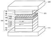
図1は、本発明の第1の実施の形態に係る磁気抵抗効果素子(CCP−CPP素子)を表す斜視図である。なお、図1および以降の図は全て模式図であり、図上での膜厚同士の比率と、実際の膜厚同士の比率は必ずしも一致しない。
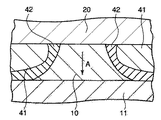
図1に示すように本実施の形態に係る磁気抵抗効果素子は、磁気抵抗効果膜10、およびこれを上下から夾む下電極11および上電極20を有し、図示しない基板上に構成される。
Hereinafter, embodiments of the present invention will be described with reference to the drawings. In the following embodiments, the composition of the alloy is expressed in atomic%.
(First embodiment)
FIG. 1 is a perspective view showing a magnetoresistive effect element (CCP-CPP element) according to a first embodiment of the present invention. Note that FIG. 1 and the subsequent drawings are all schematic views, and the ratio between the film thicknesses in the figure does not necessarily match the ratio between the actual film thicknesses.
As shown in FIG. 1, the magnetoresistive effect element according to the present embodiment has a
磁気抵抗効果膜10は、下地層12、ピニング層13、ピン層14、下部金属層15、スペーサ層(CCP−NOL)16(絶縁層161、電流パス162)、上部金属層17、フリー層18、キャップ層19が順に積層されて構成される。この内、ピン層14、下部金属層15、スペーサ層16、および上部金属層17、およびフリー層18が、2つの強磁性層の間に非磁性のスペーサ層を挟んでなるスピンバルブ膜に対応する。また、下部金属層15、スペーサ層(CCP−NOL)16、および上部金属層17の全体が広義のスペーサ層として定義される。なお、見やすさのために、スペーサ層16はその上下層(下部金属層15および上部金属層17)から切り離した状態で表している。
The
以下、磁気抵抗効果素子の構成要素を説明する。
下電極11は、スピンバルブ膜の垂直方向に通電するための電極である。下電極11と上電極20との間に電圧が印加されることで、スピンバルブ膜内部をその膜垂直方向に沿って電流が流れる。この電流によって、磁気抵抗効果に起因する抵抗の変化を検出することで、磁気の検知が可能となる。下電極11には、電流を磁気抵抗効果素子に通電するために、電気抵抗が比較的小さい金属層が用いられる。
Hereinafter, components of the magnetoresistive element will be described.
The
下地層12は、例えば、バッファ層12a、シード層12bに区分することができる。バッファ層12aは下電極11表面の荒れを緩和したりするための層である。シード層12bは、その上に成膜されるスピンバルブ膜の結晶配向および結晶粒径を制御するための層である。
The
バッファ層12aとしては、Ta、Ti、W、Zr、Hf、Crまたはこれらの合金を用いることができる。バッファ層12aの膜厚は2〜10nm程度が好ましく、3〜5nm程度がより好ましい。バッファ層12aの厚さが薄すぎるとバッファ効果が失われる。一方、バッファ層12aの厚さが厚すぎるとMR変化率に寄与しない直列抵抗を増大させることになる。なお、バッファ層12a上に成膜されるシード層12bがバッファ効果を有する場合には、バッファ層12aを必ずしも設ける必要はない。上記のなかの好ましい一例として、Ta[3nm]を用いることができる。 As the buffer layer 12a, Ta, Ti, W, Zr, Hf, Cr, or an alloy thereof can be used. The thickness of the buffer layer 12a is preferably about 2 to 10 nm, and more preferably about 3 to 5 nm. If the buffer layer 12a is too thin, the buffer effect is lost. On the other hand, if the buffer layer 12a is too thick, the series resistance that does not contribute to the MR change rate is increased. When the seed layer 12b formed on the buffer layer 12a has a buffer effect, the buffer layer 12a is not necessarily provided. As a preferred example of the above, Ta [3 nm] can be used.
シード層12bは、その上に成膜される層の結晶配向を制御できる材料であればよい。シード層12bとして、fcc構造(face-centered cubic structure:面心立方格子構造)またはhcp構造(hexagonal close-packed structure:六方最密格子構造)やbcc構造(body-centered cubic structure:体心立方格子構造)を有する金属層などが好ましい。例えば、シード層12bとして、hcp構造を有するRuや、fcc構造を有するNiFeを用いることにより、その上のスピンバルブ膜の結晶配向をfcc(111)配向にすることができる。また、ピニング層13(例えば、PtMn)の結晶配向を規則化したfct構造(face-centered tetragonal structure:面心正方構造)、あるいはbcc(body-centered cubic structure:体心立方構造)(110)配向とすることができる。
結晶配向を向上させるシード層12bとしての機能を十分発揮するために、シード層12bの膜厚としては、1〜5nmが好ましく、より好ましくは、1.5〜3nmが好ましい。上記のなかの好ましい一例として、Ru[2nm]を用いることができる。
The seed layer 12b may be any material that can control the crystal orientation of the layer formed thereon. As the seed layer 12b, an fcc structure (face-centered cubic structure), an hcp structure (hexagonal close-packed structure), or a bcc structure (body-centered cubic structure) A metal layer having a structure is preferable. For example, by using Ru having an hcp structure or NiFe having an fcc structure as the seed layer 12b, the crystal orientation of the spin valve film thereon can be changed to the fcc (111) orientation. Further, the fct structure (face-centered tetragonal structure) in which the crystal orientation of the pinning layer 13 (for example, PtMn) is regularized, or bcc (body-centered cubic structure) (110) orientation It can be.
In order to sufficiently exhibit the function as the seed layer 12b for improving the crystal orientation, the film thickness of the seed layer 12b is preferably 1 to 5 nm, more preferably 1.5 to 3 nm. As a preferred example of the above, Ru [2 nm] can be used.
スピンバルブ膜やピニング層13の結晶配向性は、X線回折により測定できる。スピンバルブ膜のfcc(111)ピーク、ピニング層13(PtMn)のfct(111)ピークまたはbcc(110)ピークでのロッキングカーブの半値幅を3.5〜6度として、良好な配向性を得ることができる。なお、この配向の分散角は断面TEMを用いた回折スポットからも判別することができる。
The crystal orientation of the spin valve film and the
シード層12bとして、Ruの代わりに、NiFeベースの合金(例えば、NixFe100−x(x=90〜50%、好ましくは75〜85%)や、NiFeに第3元素Xを添加して非磁性にした(NixFe100−x)100−yXy(X=Cr、V、Nb、Hf、Zr、Mo))を用いることもできる。NiFeベースのシード層12bでは、良好な結晶配向性を得るのが比較的容易であり、上記と同様に測定したロッキングカーブの半値幅を3〜5度とすることができる。 As the seed layer 12b, a NiFe-based alloy (for example, Ni x Fe 100-x (x = 90 to 50%, preferably 75 to 85%) or a third element X is added to NiFe instead of Ru. and the non-magnetic (Ni x Fe 100-x) 100-y X y (X = Cr, V, Nb, Hf, Zr, Mo)) can also be used. In the NiFe-based seed layer 12b, it is relatively easy to obtain good crystal orientation, and the half-value width of the rocking curve measured in the same manner as described above can be 3 to 5 degrees.
シード層12bには、結晶配向を向上させる機能だけでなく、スピンバルブ膜の結晶粒径を制御する機能もある。具体的には、スピンバルブ膜の結晶粒径を5〜40nmに制御することができ、磁気抵抗効果素子のサイズが小さくなっても、特性のばらつきを招くことなく高いMR変化率を実現できる。
ここでの結晶粒径は、シード層12bの上に形成された結晶粒の粒径によって判別することができ、断面TEMなどによって決定することができる。ピン層14がスペーサ層16よりも下層に位置するボトム型スピンバルブ膜の場合には、シード層12bの上に形成される、ピニング層13(反強磁性層)や、ピン層14(磁化固着層)の結晶粒径によって判別することができる。
The seed layer 12b has not only a function of improving the crystal orientation but also a function of controlling the crystal grain size of the spin valve film. Specifically, the crystal grain size of the spin valve film can be controlled to 5 to 40 nm, and even when the size of the magnetoresistive element is reduced, a high MR change rate can be realized without causing variations in characteristics.
The crystal grain size here can be determined by the grain size of the crystal grains formed on the seed layer 12b, and can be determined by a cross-sectional TEM or the like. When the pinned
高密度記録に対応した再生ヘッドでは、素子サイズが、例えば、100nm以下である。素子サイズに対する結晶粒径の比が大きいことは、素子の特性がばらつく原因となる。スピンバルブ膜の結晶粒径が40nmよりも大きいことは好ましくない。具体的には、結晶粒径が5〜40nmの範囲が好ましく、5〜20nmの範囲がさらに好ましい範囲である。 In a reproducing head compatible with high-density recording, the element size is, for example, 100 nm or less. A large ratio of the crystal grain size to the element size causes variations in element characteristics. It is not preferable that the crystal grain size of the spin valve film is larger than 40 nm. Specifically, the crystal grain size is preferably in the range of 5 to 40 nm, and more preferably in the range of 5 to 20 nm.
素子面積あたりの結晶粒の数が少なくなると、結晶数が少ないことに起因した特性のばらつきの原因となりうるため、結晶粒径を大きくすることはあまり好ましくない。特に電流パスを形成しているCCP−CPP素子では結晶粒径を大きくすることはあまり好ましくない。一方、結晶粒径が小さくなりすぎても、良好な結晶配向を維持することが一般的には困難になる。これら、結晶粒径の上限、および下限を考慮した結晶粒径の好ましい範囲が、5〜20nmである。
しかしながら、MRAM用途などでは、素子サイズが100nm以上の場合があり、結晶粒径が40nm程度と大きくてもそれほど問題とならない場合もある。即ち、シード層12bを用いることで、結晶粒径が粗大化しても差し支えない場合もある。
When the number of crystal grains per element area decreases, it may cause variation in characteristics due to the small number of crystals, so it is not preferable to increase the crystal grain size. In particular, it is not preferable to increase the crystal grain size in a CCP-CPP element in which a current path is formed. On the other hand, it is generally difficult to maintain good crystal orientation even if the crystal grain size becomes too small. A preferable range of the crystal grain size in consideration of the upper limit and the lower limit of the crystal grain size is 5 to 20 nm.
However, in MRAM applications and the like, the element size may be 100 nm or more, and even if the crystal grain size is as large as about 40 nm, there may be no problem. That is, by using the seed layer 12b, the crystal grain size may be increased in some cases.
上述した5〜20nmの結晶粒径を得るためには、シード層12bとして、Ru2nmや、(NixFe100−x)100−yXy(X=Cr、V、Nb、Hf、Zr、Mo))層の場合には、第3元素Xの組成yを0〜30%程度とすることが好ましい(yが0%の場合も含む)。
一方、結晶粒径を40nmよりも粗大化させて用いるためには、さらに多量の添加元素を用いることが好ましい。シード層12bの材料が、例えば、NiFeCrの場合にはCr量を35〜45%程度とし、fccとbccの境界相を示す組成を用いて、bcc構造を有するNiFeCr層を用いることが好ましい。
In order to obtain the crystal grain size of 5~20nm described above, as the seed layer 12b, Ru2nm and, (Ni x Fe 100-x ) 100-y X y (X = Cr, V, Nb, Hf, Zr, Mo )) In the case of a layer, the composition y of the third element X is preferably about 0 to 30% (including the case where y is 0%).
On the other hand, in order to use the crystal grain size coarser than 40 nm, it is preferable to use a larger amount of additive element. When the material of the seed layer 12b is, for example, NiFeCr, it is preferable to use a NiFeCr layer having a bcc structure with a Cr amount of about 35 to 45% and a composition showing a boundary phase between fcc and bcc.
前述したように、シード層12bの膜厚は1nm〜5nm程度が好ましく、1.5〜3nmがより好ましい。シード層12bの厚さが薄すぎると結晶配向制御などの効果が失われる。一方、シード層12bの厚さが厚すぎると、直列抵抗の増大を招き、さらにスピンバルブ膜の界面の凹凸の原因となることがある。 As described above, the thickness of the seed layer 12b is preferably about 1 nm to 5 nm, and more preferably 1.5 to 3 nm. If the thickness of the seed layer 12b is too thin, effects such as crystal orientation control are lost. On the other hand, if the thickness of the seed layer 12b is too thick, the series resistance may be increased, and unevenness at the interface of the spin valve film may be caused.
ピニング層13は、その上に成膜されるピン層14となる強磁性層に一方向異方性(unidirectional anisotropy)を付与して磁化を固着する機能を有する。ピニング層13の材料としては、PtMn、PdPtMn、IrMn、RuRhMnなどの反強磁性材料を用いることができる。この内、高記録密度対応のヘッドの材料として、IrMnが有利である。IrMnは、PtMnよりも薄い膜厚で一方向異方性を印加することができ、高密度記録の為に必要な狭ギャップ化に適している。
The pinning
十分な強さの一方向異方性を付与するために、ピニング層13の膜厚を適切に設定する。ピニング層13の材料がPtMnやPdPtMnの場合には、膜厚として、8〜20nm程度が好ましく、10〜15nmがより好ましい。ピニング層13の材料がIrMnの場合には、PtMnなどより薄い膜厚でも一方向異方性を付与可能であり、4〜18nmが好ましく、5〜15nmがより好ましい。上記のなかの好ましい一例として、IrMn[10nm]を用いることができる。
In order to impart sufficient strength of unidirectional anisotropy, the film thickness of the pinning
ピニング層13として、反強磁性層の代わりに、ハード磁性層を用いることができる。ハード磁性層として、例えば、CoPt(Co=50〜85%)、(CoxPt100−x)100−yCry(x=50〜85%、y=0〜40%)、FePt(Pt=40〜60%)を用いることができる。ハード磁性層(特に、CoPt)は比抵抗が比較的小さいため、直列抵抗および面積抵抗RAの増大を抑制できる。
As the pinning
ピン層14は、下部ピン層141(例えば、Co90Fe103.5nm)、磁気結合層142(例えば、Ru)、および上部ピン層143(例えば、Fe50Co50[1nm]/Cu[0.25nm])×2/Fe50Co50[1nm])からなるシンセティックピン層とすることのが好ましい一例である。ピニング層13(例えば、IrMn)とその直上の下部ピン層141は一方向異方性(unidirectional anisotropy)をもつように交換磁気結合している。磁気結合層142の上下の下部ピン層141および上部ピン層143は、磁化の向きが互いに反平行になるように強く磁気結合している。
The pinned
下部ピン層141の材料として、例えば、CoxFe100−x合金(x=0〜100%)、NixFe100−x合金(x=0〜100%)、またはこれらに非磁性元素を添加したものを用いることができる。また、下部ピン層141の材料として、Co、Fe、Niの単元素やこれらの合金を用いても良い。
As a material of the lower pinned
下部ピン層141の磁気膜厚(飽和磁化Bs×膜厚t(Bs・t積))が、上部ピン層143の磁気膜厚とほぼ等しいことが好ましい。つまり、上部ピン層143の磁気膜厚と下部ピン層141の磁気膜厚とが対応することが好ましい。一例として、上部ピン層143が(Fe50Co50[1nm]/Cu[0.25nm])×2/Fe50Co50[1nm]の場合、薄膜でのFeCoの飽和磁化が約2.2Tであるため、磁気膜厚は2.2T×3nm=6.6Tnmとなる。Co90Fe10の飽和磁化が約1.8Tなので、上記と等しい磁気膜厚を与える下部ピン層141の膜厚tは6.6Tnm/1.8T=3.66nmとなる。したがって、膜厚が約3.6nmのCo90Fe10を用いることが望ましい。
The magnetic film thickness (saturation magnetization Bs × film thickness t (Bs · t product)) of the lower pinned
下部ピン層141に用いられる磁性層の膜厚は2〜5nm程度が好ましい。ピニング層13(例えば、IrMn)による一方向異方性磁界強度および磁気結合層142(例えば、Ru)を介した下部ピン層141と上部ピン層143との反強磁性結合磁界強度の観点に基づく。下部ピン層141が薄すぎるとMR変化率が小さくなる。一方、下部ピン層141が厚すぎるとデバイス動作に必要な十分な一方向性異方性磁界を得ることが困難になる。好ましい一例として、膜厚3.6nmのCo90Fe10が挙げられる。
The thickness of the magnetic layer used for the lower pinned
磁気結合層142(例えば、Ru)は、上下の磁性層(下部ピン層141および上部ピン層143)に反強磁性結合を生じさせてシンセティックピン構造を形成する機能を有する。磁気結合層142としてのRu層の膜厚は0.8〜1nmであることが好ましい。なお、上下の磁性層に十分な反強磁性結合を生じさせる材料であれば、Ru以外の材料を用いてもよい。RKKY(Ruderman-Kittel- Kasuya-Yosida)結合の2ndピークに対応する膜厚0.8〜1nmの換わりに、RKKY結合の1stピークに対応する膜厚0.3〜0.6nmを用いることもできる。ここでは、より高信頼性の結合を安定して特性が得られる、0.9nmのRuが一例として挙げられる。
The magnetic coupling layer 142 (for example, Ru) has a function of forming a synthetic pin structure by causing antiferromagnetic coupling in the upper and lower magnetic layers (lower pinned
上部ピン層143の一例として、(Fe50Co50[1nm]/Cu[0.25nm])×2/Fe50Co50[1nm]のような磁性層を用いることができる。上部ピン層143は、スピン依存散乱ユニットの一部をなす。上部ピン層143は、MR効果に直接的に寄与する磁性層であり、大きなMR変化率を得るために、この構成材料、膜厚の双方が重要である。特に、スペーサ層16との界面に位置する磁性材料は、スピン依存界面散乱に寄与する点で特に重要である。
As an example of the upper pinned
上部ピン層143としてここで用いた、bcc構造をもつFe50Co50を用いる効果について述べる。上部ピン層143として、bcc構造をもつ磁性材料を用いた場合、スピン依存界面散乱効果が大きいため、大きなMR変化率を実現することができる。bcc構造をもつFeCo系合金として、FexCo100−x(x=30〜100%)や、FexCo100−xに添加元素を加えたものが挙げられる。そのなかでも、諸特性を満たしたFe40Co60〜Fe60Co40が使いやすい材料の一例である。
The effect of using the Fe 50 Co 50 having the bcc structure used here as the upper pinned
上部ピン層143が、高MR変化率を実現しやすいbcc構造をもつ磁性層から形成されている場合には、この磁性層の全膜厚が1.5nm以上であることが好ましい。bcc構造を安定に保つためである。スピンバルブ膜に用いられる金属材料は、fcc構造またはfct構造であることが多いため、上部ピン層143のみがbcc構造を有することがあり得る。このため、上部ピン層143の膜厚が薄すぎると、bcc構造を安定に保つことが困難になり、高いMR変化率が得られなくなる。
ここでは、上部ピン層143として、極薄Cu積層を含むFe50Co50を用いている。ここで、上部ピン層143は、全膜厚が3nmのFeCoと、1nmのFeCo毎に積層された0.25nmのCuとからなり、トータル膜厚3.5nmである。
When the upper pinned
Here, as the upper pinned
上部ピン層143の膜厚は5nm以下であることが好ましい。大きなピン固着磁界を得るためである。大きなピン固着磁界と、bcc構造の安定性の両立のため、bcc構造をもつ上部ピン層143の膜厚は、2.0nm〜4nm程度であることが好ましいということになる。
The film thickness of the upper pinned
上部ピン層143には、bcc構造をもつ磁性材料の代わりに、従来の磁気抵抗効果素子で広く用いられているfcc構造を有するCo90Fe10合金や、hcp構造をもつコバルト合金を用いることができる。上部ピン層143として、Co、Fe、Niなどの単体金属、またはこれらのいずれか一つの元素を含む合金材料はすべて用いることができる。上部ピン層143の磁性材料として、大きなMR変化率を得るのに有利なものから並べると、bcc構造をもつFeCo合金材料、50%以上のコバルト組成をもつコバルト合金、50%以上のNi組成をもつニッケル合金の順になる。
For the upper pinned
ここでの一例として挙げたものは、上部ピン層143として、磁性層(FeCo層)と非磁性層(極薄Cu層)とを交互に積層したものを用いることができる。このような構造を有する上部ピン層143では、極薄Cu層によって、スピン依存バルク散乱効果と呼ばれるスピン依存散乱効果を向上させることができる。
「スピン依存バルク散乱効果」は、スピン依存界面散乱効果と対の言葉として用いられる。スピン依存バルク散乱効果とは、磁性層内部でMR効果を発現する現象である。スピン依存界面散乱効果は、スペーサ層と磁性層の界面でMR効果を発現する現象である。
As an example here, as the upper pinned
The “spin-dependent bulk scattering effect” is used as a paired term with the spin-dependent interface scattering effect. The spin-dependent bulk scattering effect is a phenomenon that manifests the MR effect inside the magnetic layer. The spin-dependent interface scattering effect is a phenomenon in which the MR effect is exhibited at the interface between the spacer layer and the magnetic layer.
以下、磁性層と非磁性層の積層構造によるバルク散乱効果の向上につき説明する。
CCP−CPP素子においては、スペーサ層16の近傍で電流が狭窄されるため、スペーサ層16の界面近傍での抵抗の寄与が非常に大きい。つまり、スペーサ層16と磁性層(ピン層14、フリー層18)の界面での抵抗が、磁気抵抗効果素子全体の抵抗に占める割合が大きい。このことは、スピン依存界面散乱効果の寄与がCCP−CPP素子では非常に大きく、重要であることを示している。つまり、スペーサ層16の界面に位置する磁性材料の選択が従来のCPP素子の場合と比較して、重要な意味をもつ。これが、ピン層143として、スピン依存界面散乱効果が大きいbcc構造をもつFeCo合金層を用いた理由であり、前述したとおりである。
Hereinafter, the improvement of the bulk scattering effect by the laminated structure of the magnetic layer and the nonmagnetic layer will be described.
In the CCP-CPP element, since the current is confined in the vicinity of the
しかしながら、バルク散乱効果の大きい材料を用いることも無視できず、より高MR変化率を得るためにはやはり重要である。バルク散乱効果を得るための極薄Cu層の膜厚は、0.1〜1nmが好ましく、0.2〜0.5nmがより好ましい。Cu層の膜厚が薄すぎると、バルク散乱効果を向上させる効果が弱くなる。Cu層の膜厚が厚すぎると、バルク散乱効果が減少することがあるうえに、非磁性のCu層を介した上下磁性層の磁気結合が弱くなり、ピン層14の特性が不十分となる。そこで、好ましい一例として挙げたものでは、0.25nmのCuを用いた。
However, the use of a material having a large bulk scattering effect cannot be ignored, and it is still important to obtain a higher MR change rate. The film thickness of the ultrathin Cu layer for obtaining the bulk scattering effect is preferably 0.1 to 1 nm, and more preferably 0.2 to 0.5 nm. If the thickness of the Cu layer is too thin, the effect of improving the bulk scattering effect is weakened. If the Cu layer is too thick, the bulk scattering effect may be reduced, and the magnetic coupling of the upper and lower magnetic layers via the nonmagnetic Cu layer will be weak, and the characteristics of the pinned
磁性層間の非磁性層の材料として、Cuの換わりに、Hf、Zr、Tiなどを用いてもよい。一方、これら極薄の非磁性層を挿入した場合、FeCoなど磁性層の一層あたりの膜厚は0.5〜2nmが好ましく、1〜1.5nm程度がより好ましい。 As a material for the nonmagnetic layer between the magnetic layers, Hf, Zr, Ti, or the like may be used instead of Cu. On the other hand, when these ultrathin nonmagnetic layers are inserted, the film thickness of one magnetic layer such as FeCo is preferably 0.5 to 2 nm, more preferably about 1 to 1.5 nm.
上部ピン層143として、FeCo層とCu層との交互積層構造に換えて、FeCoとCuを合金化した層を用いてもよい。このようなFeCoCu合金として、例えば、(FexCo100-x)100-yCuy(x=30〜100%、y=3〜15%程度)が挙げられるが、これ以外の組成範囲を用いてもよい。ここで、FeCoに添加する元素として、Cuの代わりに、Hf、Zr,Tiなど他の元素を用いてもよい。
上部ピン層143には、Co、Fe、Niや、これらの合金材料からなる単層膜を用いてもよい。例えば、最も単純な構造の上部ピン層143として、従来から広く用いられている、2〜4nmのCo90Fe10単層を用いてもよい。この材料に他の元素を添加してもよい。
As the upper pinned
The upper pinned
次に、広義のスペーサ層を形成する膜構成について述べる。下部金属層15は、電流パス162の形成に用いられ、いわば電流パス162の供給源である。ただし、電流パス162の形成後にも明確な金属層として残存している必要はない。下部金属層15は、広義のスペーサ層の一部を形成する材料である。下部金属層15は、その上部のスペーサ層16を形成するときに、下部に位置する磁性層143の酸化を抑制するストッパ層としての機能も有する。
Next, a film configuration for forming the spacer layer in a broad sense will be described. The
スペーサ層(CCP−NOL)16は、絶縁層161、電流パス162を有する。なお、前述のように、スペーサ層16、下部金属層15、および上部金属層17を含めて、広義のスペーサ層として取り扱う。
絶縁層161は、酸化物、窒化物、酸窒化物等から構成される。絶縁層161として、Al2O3のようなアモルファス構造や、MgOのような結晶構造の双方が有り得る。スペーサ層としての機能を発揮するために、絶縁層161の厚さは、1〜3nmが好ましく、1.5〜2.5nmの範囲がより好ましい。
The spacer layer (CCP-NOL) 16 includes an insulating
The insulating
絶縁層161に用いる典型的な絶縁材料として、Al2O3をベース材料としたものや、これに添加元素を加えたものがある。添加元素として、Ti、Hf、Mg、Zr,V,Mo、Si,Cr,Nb,Ta,W、B,C、Vなどがある。これらの添加元素の添加量は0%〜50%程度の範囲で適宜変えることができる。一例として、約2nmのAl2O3を絶縁層161として用いることができる。
As a typical insulating material used for the insulating
絶縁層161には、Al2O3のようなAl酸化物の換わりに、Ti酸化物、Hf酸化物、Mg酸化物、Zr酸化物、Cr酸化物、Ta酸化物、Nb酸化物、Mo酸化物、Si酸化物、V酸化物なども用いることができる。これらの酸化物の場合でも、添加元素として上述の材料を用いることができる。また、添加元素の量を0%〜50%程度の範囲で適宜に変えることができる。
これら酸化物の換わりに、上述したようなAl,Si,Hf,Ti,Mg,Zr,V,Mo,Nb,Ta,W,B,Cをベースとした酸窒化物や、窒化物を用いても、電流を絶縁する機能を有する材料であれば構わない。
For the insulating
Instead of these oxides, oxynitrides and nitrides based on Al, Si, Hf, Ti, Mg, Zr, V, Mo, Nb, Ta, W, B, and C as described above are used. However, any material having a function of insulating current may be used.
電流パス162は、スペーサ層16の膜面垂直に電流を流すパス(経路)であり、電流を狭窄するためのものである。絶縁層161の膜面垂直方向に電流を通過させる導電体として機能し、例えば、Cu等の金属層から構成できる。即ち、スペーサ層16では、電流狭窄構造(CCP構造)を有し、電流狭窄効果によりMR変化率を増大可能である。電流パス162(CCP)を形成する材料は、Cu以外には、Au,Agや、Ni,Co,Fe、もしくはこれらの元素を少なくとも一つは含む合金層を挙げることができる。一例として、電流パス162をCuを含む合金層で形成することができる。CuNi、CuCo、CuFeなどの合金層も用いることができる。ここで、50%以上のCuを有する組成とすることが、高MR変化率と、ピン層14とフリー層18の層間結合磁界(interlayer coupling field, Hin)を小さくするためには好ましい。
電流パス162は絶縁層161と比べて著しく酸素、窒素の含有量が少ない領域であり(少なくとも2倍以上の酸素や窒素の含有量の差がある)、一般的には結晶相である。結晶相は非結晶相よりも抵抗が小さいため、電流パス162として機能しやすい。
The
The
上部金属層17は、広義のスペーサ層の一部を形成するものである。その上に成膜されるフリー層18がスペーサ層16の酸化物に接して酸化されないように保護するバリア層としての機能、およびフリー層18の結晶性を良好にする機能を有する。例えば、絶縁層161の材料がアモルファス(例えば、Al2O3)の場合には、その上に成膜される金属層の結晶性が悪くなるが、fcc結晶性を良好にする層(例えば、Cu層)を配置することで(1nm以下程度の膜厚で良い)、フリー層18の結晶性を著しく改善することが可能となる。
The
スペーサ層16の材料やフリー層18の材料によっては、必ずしも上部金属層17を設けなくてもよい。アニール条件の最適化や、スペーサ層16の絶縁層161材料の選択、フリー層18の材料などによって、結晶性の低下を回避し、スペーサ層16上の金属層17が不要にできる。
しかし、製造上のマージンを考慮すると、スペーサ層16上に上部金属層17を形成することが好ましい。好ましい一例としては、上部金属層17として、Cu[0.5nm]を用いることができる。
Depending on the material of the
However, considering the manufacturing margin, it is preferable to form the
上部金属層17の構成材料として、Cu以外に、Au、Ag、Ruなどを用いることもできる。上部金属層17の材料は、スペーサ層16の電流パス162の材料と同一であることが好ましい。上部金属層17の材料が電流パス162の材料と異なる場合には界面抵抗の増大を招くが、両者が同一の材料であれば界面抵抗の増大は生じない。
As a constituent material of the
上部金属層17の膜厚は、0〜1nmが好ましく、0.1〜0.5nmがより好ましい。上部金属層17が厚すぎると、スペーサ層16で狭窄された電流が上部金属層17で広がって電流狭窄効果が不十分になり、MR変化率の低下を招く。
The thickness of the
フリー層18は、磁化方向が外部磁界によって変化する強磁性体を有する層である。例えば、界面にCoFeを挿入してNiFeを用いたCo90Fe10[1nm]/Ni83Fe17[3.5nm]という二層構成がフリー層18の一例として挙げられる。この場合、スペーサ層16との界面には、NiFe合金よりもCoFe合金を設けることが好ましい。高いMR変化率を得るためには、スペーサ層16の界面に位置するフリー層18の磁性材料の選択が重要である。なお、NiFe層を用いない場合には、Co90Fe10[4nm]単層を用いることができる。また、CoFe/NiFe/CoFeなどの三層構成からなるフリー層を用いても構わない。
The
CoFe合金のなかでも、軟磁気特性が安定であることから、Co90Fe10が好ましい。Co90Fe10近傍のCoFe合金を用いる場合には、膜厚を0.5〜4nmとすることが好ましい。その他、CoxFe100−x(x=70〜90)が好ましい。
また、フリー層18として、1〜2nmのCoFe層またはFe層と、0.1〜0.8nm程度の極薄Cu層とを、複数層交互に積層したものを用いてもよい。
Among the CoFe alloys, Co 90 Fe 10 is preferable because the soft magnetic characteristics are stable. When a CoFe alloy near Co 90 Fe 10 is used, the film thickness is preferably 0.5 to 4 nm. In addition, Co x Fe 100-x (x = 70 to 90) is preferable.
Further, as the
スペーサ層16がCu層から形成される場合には、ピン層14と同様に、フリー層18でも、bccのFeCo層をスペーサ層16との界面材料として用いると、MR変化率が大きくなる。スペーサ層16との界面材料として、fccのCoFe合金に換えて、bccのFeCo合金を用いることもできる。この場合、bcc層が形成されやすい、FexCo100−x(x=30〜100)や、これに添加元素を加えた材料を用いることができる。これらの構成のうち、好ましい実施例の一例として、Co90Fe10[1nm]/Ni83Fe17[3.5nm]を用いることができる。
When the
ここで、本実施形態のポイントは、CCP−NOL上に形成された磁性層、ここで実施例としてあげたボトム型スピンバルブ膜の場合にはフリー層18中の少なくとも一部を応力調整部21とすることで、素子の信頼性を著しく改善することができる。広義のスペーサ層の下に形成された磁性層(ピン層14)の結晶性と、広義のスペーサ層の上に形成された磁性層(フリー層18)の結晶性が著しく異なることに起因して、本処理が絶大な効果を発揮することになる。この処理の詳細については後述する。
Here, the point of the present embodiment is that in the case of the magnetic layer formed on the CCP-NOL, that is, the bottom type spin valve film mentioned here as an example, at least a part of the
キャップ層19は、スピンバルブ膜を保護する機能を有する。キャップ層19は、例えば、複数の金属層、例えば、Cu層とRu層の2層構造(Cu[1nm]/Ru[10nm])とすることができる。また、キャップ層19として、Ruをフリー層18側に配置したRu/Cu層なども用いることができる。この場合、Ruの膜厚は0.5〜2nm程度が好ましい。この構成のキャップ層19は、特に、フリー層18がNiFeからなる場合に望ましい。RuはNiと非固溶な関係にあるので、フリー層18とキャップ層19の間に形成される界面ミキシング層の磁歪を低減できるからである。
キャップ層19が、Cu/Ru、Ru/Cu、いずれの場合も、Cu層の膜厚は0.5〜10nm程度が好ましく、Ru層の膜厚は0.5〜5nm程度とすることができる。Ruは比抵抗値が高いため、あまり厚いRu層を用いることは好ましくないため、このような膜厚範囲にしておくことが好ましい。
The
When the
キャップ層19として、Cu層やRu層の代わりに他の金属層を設けてもよい。キャップ層19の構成は特に限定されず、キャップとしてスピンバルブ膜を保護可能なものであれば、他の材料を用いてもよい。但し、キャップ層の選択によってMR変化率や長期信頼性が変わる場合があるので、注意が必要である。CuやRuはこれらの観点からも望ましいキャップ層の材料の例である。
As the
上電極20は、スピンバルブ膜の垂直方向に通電するための電極である。下電極11と上電極20との間に電圧が印加されることで、スピンバルブ膜内部にその膜の垂直方向の電流が流れる。上部電極層20には、電気的に低抵抗な材料(例えば、Cu,Au)が用いられる。
The
(応力調整部21の意義)
ここで本実施形態に特徴的な応力調整部21について詳細に説明する。応力調整部21とは、スペーサ層(CCP−NOL)16上に形成された磁性層の製造過程において応力調整処理(Strain Control Treatment: SCT)が施された領域である。一例として、フリー層18が上述のようなCoFe/NiFeで形成された場合、フリー層18全体を応力調整部21と観念できる。
なお、フリー層18中に応力調整処理された領域(応力調整部21)と、応力調整処理がされない領域とが存在する場合、これらの間に明確な境界が存在しないのが通例である。
(Significance of the stress adjustment unit 21)
Here, the
In addition, when there exists the area | region (stress adjustment part 21) in which the stress adjustment process was carried out in the
本実施形態では、ピン層14が広義のスペーサ層よりも下層側に配置されているので(ボトム型スピンバルブ膜)、スペーサ層(CCP−NOL)16上に形成された磁性層はフリー層18となる(トップ型スピンバルブ膜の場合は、スペーサ層(CCP−NOL)16上に形成された磁性層はピン層14となる)。
即ち、本実施形態では、フリー層18の一部(あるいは、全部)に応力調整処理(SCT)が施される。応力調整処理とは、フリー層18の内部応力を調整するための処理である。処理を行うことで、処理を行わない状態と比べて、フリー層18の膜残留応力をcompressive側(圧縮)にシフトさせることで、磁気抵抗効果素子の信頼性を向上することが可能となる。例えば、フリー層18の膜残留応力が大きなTensile応力(引っ張り応力)を有する場合には、そのTensile応力の絶対値を低減させることが可能となる。
なお、応力調整処理(SCT)の詳細は後述するが、応力調整処理(SCT)は磁性層の薄膜形成時に、イオン、プラズマ、および熱の何れかによる処理を意味する。
In this embodiment, since the pinned
That is, in this embodiment, a stress adjustment process (SCT) is performed on a part (or all) of the
Although details of the stress adjustment process (SCT) will be described later, the stress adjustment process (SCT) means a process using any one of ions, plasma, and heat when forming a thin film of the magnetic layer.
A.フリー層18での内部応力の発生
以下に、電流狭窄型の広義のスペーサ層の上に形成された磁性層において膜残留応力が大きくなるメカニズムについて説明する。ここでは、一例として、ピン層14がスペーサ層よりも下層側に配置された、ボトム型スピンバルブ膜の場合について述べる。ボトム型スピンバルブ膜の場合には、スペーサ層の上に形成される磁性層はフリー層18となるため、フリー層18に応力調整処理(SCT)を行うことになる。トップ型スピンバルブ膜の場合には、スペーサ層の上側に形成される磁性層はピン層14となるので、応力調整処理(SCT)を行う層は、ピン層14ということになる。
A. Generation of Internal Stress in Free Layer 18 A mechanism for increasing the film residual stress in the magnetic layer formed on the current confinement type spacer layer in the broad sense will be described below. Here, as an example, a case of a bottom type spin valve film in which the pinned
上述したように、スペーサ層16の上下の2つの強磁性層(ピン層14、フリー層18)は、Fe,Co、Niやそれらの元素を含む合金層からなり、類似の金属材料を用いて形成されている。
しかしながら、これら2つの強磁性層の結晶性が異なることが判った。具体的には、フリー層18の結晶性がピン層14の結晶性より劣る。これは、スペーサ層16の絶縁層161が結晶性の比較的劣る材料(典型的には、アルミナ(Al2O3)等のアモルファス材料)から構成されることに起因すると考えられる。アモルファス材料の上で成長する膜は、結晶性が悪いのが通例である。以上のように、フリー層18の結晶性はピン層14の結晶性より劣る。
As described above, the two ferromagnetic layers above and below the spacer layer 16 (the pinned
However, it has been found that the crystallinity of these two ferromagnetic layers is different. Specifically, the crystallinity of the
これは、CCP−NOLだけでなく、電流狭窄構造を有しない、一様なAl2O3や、MgO,TiOx層からなる、TMR膜でも共通の問題である。このことから、応力調整処理(SCT)を用いた製造方法は、TMR膜に適用することは可能である。
TMR膜の場合には、一例として、ピン層が2〜3nmのCoFe合金層やCoFeB合金層、スペーサ層が1〜2.5nmのAl2O3、TiOx、またはMgO、フリー層が1〜3nmのCoFe合金層/2〜4nmのNiFeという構成があげられる。また、フリー層にもピン層同様に、スペーサ層の絶縁層との界面にCoFeB合金層を用いても構わない。ピン層、スペーサ層、フリー層以外のRu下のピン層、反強磁性層、下地層や、フリー層上のキャップ層は前述の場合の電流狭窄型CPP素子の場合と同様である。TMR素子の場合には、スペーサ層の絶縁層材料に膜面垂直に貫通する電流パスは存在せず、膜面垂直に流れる電流はトンネル伝導により電流が流れることになる。
ボトム型スピンバルブ膜の場合には、スペーサ層の上に形成された材料はフリー層18ということになるので、フリー層18に応力調整処理SCTを行うことになる。TMR素子においても、Al2O3、TiOx、MgOなどのトンネルバリアスペーサ層の上に形成された磁性層の結晶性は、その下に形成された磁性層の結晶性に比べて悪いので、応力調整処理が効果を発揮する。
This is a common problem not only with CCP-NOL but also with a TMR film made of a uniform Al 2 O 3 , MgO, or TiOx layer having no current confinement structure. Therefore, the manufacturing method using the stress adjustment process (SCT) can be applied to the TMR film.
In the case of the TMR film, as an example, the pinned layer has a CoFe alloy layer or CoFeB alloy layer having a thickness of 2 to 3 nm, the spacer layer has a thickness of 1 to 2.5 nm, Al 2 O 3 , TiO x , or MgO, and the free layer has a thickness of 1 to Examples include a structure of 3 nm CoFe alloy layer / 2 to 4 nm NiFe. Further, a CoFeB alloy layer may be used for the free layer as well as the pinned layer at the interface between the spacer layer and the insulating layer. Other than the pin layer, spacer layer, and free layer, the pin layer under Ru, the antiferromagnetic layer, the underlayer, and the cap layer on the free layer are the same as those in the current confinement type CPP element described above. In the case of a TMR element, there is no current path that penetrates the insulating layer material of the spacer layer perpendicular to the film surface, and the current that flows perpendicular to the film surface flows by tunnel conduction.
In the case of the bottom type spin valve film, the material formed on the spacer layer is the
しかしながら、CCP−CPP素子においては、TMR素子よりもさらにシビアな問題として、CCP−NOL(電流狭窄型NOL、スペーサ層)上に形成された磁性層では、結晶性が平均的に悪いのみでなく、膜面内で不均一でもあることが判った。フリー層18は、アルミナ(Al2O3)等の酸化物の絶縁層161中に金属材料の電流パス162が配置されている。電流パス162としての金属材料は、絶縁層161を貫通して下層のピン層14と結晶的に結合し、ピン層14の結晶構造を反映した比較的良好な結晶構造となる。即ち、フリー層18は、異なる結晶構造(CCPのCuなどの金属層(電流パス162)上に成長した比較的良好な結晶構造からなる磁性層と、アモルファスAl2O3などの絶縁層161上に成長した結晶性の悪い磁性層)が二次元面内に混在したマトリックス構造となる。つまり、フリー層18の面上に、結晶構造が比較的良好な領域(電流パス162に対応)と、結晶構造が劣る領域(絶縁層161に対応)とが分布する。
However, in the CCP-CPP element, as a more severe problem than the TMR element, the magnetic layer formed on the CCP-NOL (current confinement type NOL, spacer layer) not only has poor crystallinity on average. It was also found that the film surface was non-uniform. In the
前述したように、上部金属層17(例えば、極薄Cu層)は、その上に成膜されるフリー層18の結晶性を良好にする機能を有する。しかしながら、上部金属層17だけでフリー層18の結晶配向性を良好にすることは困難である。結晶性の改善のためだけに3nm以上のCuを上部金属層17として用いて、磁性層の結晶性改善を試みるなどの手法もあるが、それは磁気抵抗効果素子としての本来の機能を失わせるので、現実的ではない。上部金属層17が1nmよりも厚くなってしまうと、MR変化率を向上させる目的のための電流狭窄効果が著しく失われてしまい、MR変化率の向上が失われてしまうからである。電流狭窄効果を効率よく得るためには、上部金属層17は1nm以下(より好ましくは、0.6nm以下)であることが好ましい。このような薄い上部金属層17で、その上に形成される磁性層の結晶性を改善することが極めて困難であることから、本実施形態のような応力調整処理が必要になる。
As described above, the upper metal layer 17 (for example, an ultrathin Cu layer) has a function of improving the crystallinity of the
フリー層18の結晶配向性の不良は、フリー層18内の大きな応力(特に、引っ張り(Tensile)応力)の発生原因となる。このような状況は、後述のように、フリー層18の内部応力は磁気抵抗効果素子の信頼性が低下する要因となり得る。
The poor crystal orientation of the
さらに、CCP−CPP素子ではTMR素子と異なり、スペーサ層を膜面垂直に通電する電流は、すべて金属層間を伝導する、金属伝導であり、TMR素子における絶縁層を介したトンネル伝導とは異なる。金属伝導ではジュール発熱がより顕著に生じ、さらにはCCPでは大きな電流密度によるジュール発熱が局所的に集中するため、TMR素子よりも熱的条件がシビアになる。
CCP−CPP素子は、スペーサ層を膜面垂直に流れる電流が金属伝導であることに起因して、低抵抗が実現容易であることから、高転送レートに適用し易い。またCCP−CPP素子は、TMR素子では避けられない問題である、トンネル伝導に起因したショットノイズの問題がなく、良好なS/N比(Signal to Noise Ratio)を得やすい。このように、CCP−CPP素子は、高密度化、および高転送レート対応の高密度ヘッドに向いており、TMR素子よりも大きなメリットがある。しかし、CCP−CPP素子は、電流が局所的に通電されるCCP部において金属伝導であることに起因して、CCP部において局所的にジュール発熱が生じる。局所的な発熱はCCP特有の問題であるため、高温環境下において使用するためには、CCP−CPP素子ではTMR素子よりも膜制御を完全にする必要がある。
Furthermore, in the CCP-CPP element, unlike the TMR element, the current flowing through the spacer layer perpendicularly to the film surface is all metal conduction conducted between the metal layers, and is different from the tunnel conduction through the insulating layer in the TMR element. In metal conduction, Joule heat generation occurs more remarkably, and in CCP, Joule heat generation due to a large current density is locally concentrated, so that the thermal condition is severer than that of a TMR element.
The CCP-CPP element can be easily applied to a high transfer rate because low resistance can be easily realized due to the fact that the current flowing through the spacer layer perpendicular to the film surface is metal conduction. The CCP-CPP element does not have a problem of shot noise caused by tunnel conduction, which is an inevitable problem with a TMR element, and it is easy to obtain a good S / N ratio (Signal to Noise Ratio). As described above, the CCP-CPP element is suitable for a high-density head corresponding to a high density and a high transfer rate, and has a larger merit than the TMR element. However, in the CCP-CPP element, Joule heat is locally generated in the CCP due to metal conduction in the CCP where current is locally passed. Since local heat generation is a problem peculiar to CCP, in order to use it in a high temperature environment, the CCP-CPP element needs to have more complete film control than the TMR element.
B.応力調整による磁気抵抗効果素子の信頼性の向上
フリー層18の内部応力が磁気抵抗効果素子の信頼性に与える影響につき説明する。
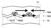
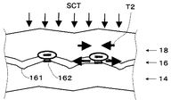
図2A、図2Bはそれぞれ、応力調整処理(SCT)がされないスピンバルブ膜、応力調整処理(SCT)がされたスピンバルブ膜(ピン層14/スペーサ層16/フリー層18)を表す模式図である。ここでは、状況を顕著に表すため、実際には使用しないような高ストレス環境下での状況を模式的に表している。
B. Improvement of Reliability of Magnetoresistive Element by Stress Adjustment The influence of the internal stress of the
2A and 2B are schematic views showing a spin valve film not subjected to stress adjustment processing (SCT) and a spin valve film (pinned
また、ここではピン層14がスペーサ層16よりも下層側に配置されたボトム型スピンバルブ膜の例で示しているが、ピン層14がスペーサ層16よりも上層側に配置されたトップ型スピンバルブ膜でも状況は同様である。トップ型スピンバルブ膜の場合には、応力調整処理(SCT)はスペーサ層16よりも上層側に形成されたピン層14に行うことになる。以下の説明でも、トップ型の場合にはフリー層18とピン層14を入れ替えれば、本質的なSCTの効果は全く同様である。
In addition, here, a bottom type spin valve film in which the pinned
図2Aのスピンバルブ膜では、応力調整処理(SCT)がされていないため、フリー層18xに大きな引張応力T1が発生しやすい。この応力T1はスペーサ層16xに印加され、スペーサ層16x、特に、フリー層18xとの界面(スピン依存散乱界面)の歪みの原因となる。歪んだ状態のスペーサ層16xを有する磁気抵抗効果素子を動作させていると、スピンバルブ膜の経時的劣化が、可逆変化・不可逆な変化、ともに生じる可能性があり、例えば、磁気抵抗効果素子の感度が低下する畏れがある。これは通常の記録密度や、使用環境が従来と同等の場合には問題にはならないが、よりシビアな高温環境下や、高速回転している状況では問題になる可能性がある。HDDの使用用途は近年益々広がっており、従来以上の高信頼性が必要とされている。 In the spin valve film of FIG. 2A, since stress adjustment processing (SCT) is not performed, a large tensile stress T1 is likely to occur in the free layer 18x. This stress T1 is applied to the spacer layer 16x and causes distortion of the interface with the spacer layer 16x, particularly the free layer 18x (spin-dependent scattering interface). When the magnetoresistive effect element having the distorted spacer layer 16x is operated, the deterioration of the spin valve film with time may occur both reversibly and irreversibly. Sensitivity may decrease. This is not a problem when the normal recording density and the use environment are the same as the conventional one, but may become a problem in a severer high temperature environment or in a state of high-speed rotation. In recent years, the usage of HDDs has been increasingly widespread, and higher reliability than ever is required.
一方、図2Bのスピンバルブ膜では、応力調整処理がされているため、フリー層18の引張応力T2が小さくなっている(大きなTensile応力が緩和される)。引張応力T2が低減されたことで、スペーサ層16やスピン依存散乱界面の歪みが小さくなる。このため、磁気抵抗効果素子を動作させたときのスピンバルブ膜の経時的劣化が小さくなる。
このように、フリー層18への応力調整処理(SCT)によって磁気抵抗効果素子の信頼性を向上することができる。ここで、応力調整処理(SCT)を行うのは、フリー層18の層中の一部であって差し支えない。SCTの条件によっては、フリー層18の一部に応力調整処理がされていれば、スペーサ層16やピン依存散乱界面の歪を低減することが可能だからである。
以上のように、フリー層18の全部または一部を応力調整処理された、応力調整部21とすることで、磁気抵抗効果素子の高度な信頼性の向上が図られる。
On the other hand, in the spin valve film of FIG. 2B, since the stress adjustment process is performed, the tensile stress T2 of the
Thus, the reliability of the magnetoresistive effect element can be improved by the stress adjustment process (SCT) to the
As described above, the reliability of the magnetoresistive effect element can be improved by using the
C.トンネル磁気抵抗素子との比較
磁気抵抗効果素子の一種に、トンネル磁気抵抗(TMR(Tunnel MagnetoResistance))素子がある。TMR素子は、2つの強磁性の間に極薄の絶縁体(以下、「TMR膜」という)を挟んで構成され、トンネル磁気抵抗効果(TMR効果)によって、磁気を検知する。
C. Comparison with tunnel magnetoresistive element One type of magnetoresistive effect element is a tunnel magnetoresistive (TMR) element. The TMR element is configured by sandwiching an extremely thin insulator (hereinafter referred to as “TMR film”) between two ferromagnets, and detects magnetism by a tunnel magnetoresistance effect (TMR effect).
TMR素子は、絶縁体を有し、その上に成長させる膜の結晶配向性が悪くなる点で、CCP−CPP素子と共通する。但し、以下(1)、(2)の理由により、スペーサ層16を有するスピンバルブ膜では、TMR膜よりも厳格な膜残留応力の調整が必要と考えられる。
The TMR element has an insulator and is common with the CCP-CPP element in that the crystal orientation of a film grown thereon is deteriorated. However, for the following reasons (1) and (2), it is considered that the spin valve film having the
(1)CCP−CPP素子では前述したように、フリー層18が、結晶性の良い部分と悪い部分とがマトリックス状に配置された複雑な構造をもつ。フリー層18の一部は、電流パス162上に形成され、ピン層14と連続する比較的良好な結晶配向性を有する。フリー層18の他の部分は、絶縁層161上に形成され、劣悪な結晶配向性を有する。このような結晶性の不均一性がフリー層18中での応力増大の要因となる。
(1) In the CCP-CPP element, as described above, the
(2)TMR膜での電流密度と比べて、スペーサ層16での電流密度が大きく、素子が発熱の影響を受けやすい。スペーサ層16では、電流が部分的に集中(狭窄)されている。このため、同じ応力を受けた場合、CCP−CPP素子のほうがTMR素子よりも熱の影響を受けやすくなる。それに対し、TMR素子では電流が膜面均一に流れることから、CCP部の局所的な電流密度と比べると電流密度の値は小さい。
以上のように、CCP−CPP素子では、膜の応力、およびその応力が信頼性に与える影響が共に大きくなり易い。
(2) Compared with the current density in the TMR film, the current density in the
As described above, in the CCP-CPP element, both the film stress and the influence of the stress on the reliability are likely to increase.
(磁気抵抗効果素子の製造方法)
以下、本実施の形態における磁気抵抗効果素子の製造方法を説明する。
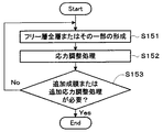
図3は、本発明の第1の実施形態に係る磁気抵抗効果素子の製造工程を表すフロー図である。
本図に示すように、下地層12〜キャップ層19が順に形成される(ステップS11〜S17)。フリー層18の形成に際して、フリー層18の全部または一部に応力調整処理(Strain Control Treatment: SCT)が施され、応力調整部21として形成される。
(Method for manufacturing magnetoresistive element)
Hereinafter, a method for manufacturing the magnetoresistive effect element according to the present embodiment will be described.
FIG. 3 is a flowchart showing manufacturing steps of the magnetoresistive effect element according to the first embodiment of the present invention.
As shown in the figure, the
A.成膜後/成膜中の応力調整処理(SCT)
応力調整処理(SCT)は、フリー層18の残留応力を調整するための処理である。以下、応力調整処理(SCT)を説明する。
応力調整処理(SCT)として、成膜後応力調整処理と成膜中応力調整処理が考えられる。
A. Stress adjustment processing after film formation / during film formation (SCT)
The stress adjustment process (SCT) is a process for adjusting the residual stress of the
As stress adjustment processing (SCT), post-deposition stress adjustment processing and during-deposition stress adjustment processing can be considered.
(1)成膜後の応力調整処理
成膜後の応力調整処理につき説明する。
図4は、図3のステップS15の詳細の一例を表し、成膜後の応力調整処理の一例を表すフロー図である。
成膜後の応力調整処理では、フリー層18の全部または一部の形成(ステップS151)後に、応力調整処理が施される(ステップS152)。追加成膜、もしくは追加応力調整処理が必要なくなるまで、これらの処理が繰り返される。例えば、図5に示すように、フリー層18が第1、第2の層181,182に区分して形成され、この区分に対応して応力調整処理がなされる。第1、第2の層181,182それぞれの表面に対する応力調整処理が可能である。ここで、後述のように、第1の層181での応力調整処理の強度を第2の層182への応力調整処理の強度より小さくすることが考えられる。スペーサ層16等への悪影響を低減するためである。
(1) Stress adjustment processing after film formation Stress adjustment processing after film formation will be described.
FIG. 4 is a flowchart showing an example of details of step S15 in FIG. 3 and showing an example of stress adjustment processing after film formation.
In the stress adjustment process after film formation, the stress adjustment process is performed (step S152) after the formation of all or part of the free layer 18 (step S151). These processes are repeated until no additional film formation or additional stress adjustment process is required. For example, as shown in FIG. 5, the
また、図5における第1、第2の層181、182において、第1の層181全体が同一の材料で形成されていなくても構わない。例えば、CoFe/NiFe二層フリー層において、CoFe層とNiFe層の一部を形成した後に、SCTを行い、残りのNiFe層を成膜した後にSCT処理を施した場合には、最初のCoFe/NiFe層が第1の層181として扱われ、残りのNiFe層が第2の層182として扱われる。
なお、この例では、フリー層18を2回に分けて成膜しているが、この回数は1回、あるいは3回以上でもよい。
Further, in the first and
In this example, the
以下、成膜後の応力調整処理を具体例において説明する。
上部金属層17(極薄Cu層)上に、フリー層18の界面材料となるCoFe合金層を形成する。このCoFe合金層として、Co90Fe10を用いることができる。また、CoFe合金層として、30%以上のFeを含有し、bcc構造のCoFe組成、具体的には、CoxFe100−x(x=95〜0)も用いることができる。CoFe合金層の膜厚は1〜2nm程度が好ましい。
Hereinafter, the stress adjustment process after film formation will be described in a specific example.
A CoFe alloy layer serving as an interface material for the
CoFe合金層の上にフリー層18の軟磁性を良好に保つためのNiFe層を形成する。NiFe層の組成として、NixFe100−x(x=75〜95atomic%)などを用いることができる。膜厚としては、1〜4nm程度が好ましい範囲である。このような積層磁性層から形成されるフリー層18の応力制御プロセスが重要となる。
A NiFe layer is formed on the CoFe alloy layer to keep the soft magnetism of the
以下、フリー層の形成をシーケンス的に説明する。フリー層18の一部として、スペーサ層16との界面層を形成するCoFe層を形成する。
この界面層の応力を改善するために、応力調整処理(SCT)を施す。SCTは、具体的には、フリー層18の少なくとも一部に、弱いエネルギー(具体的には、RFプラズマ、イオンビーム、熱など)を加えるプロセスである。
Hereinafter, the formation of the free layer will be described in sequence. As a part of the
In order to improve the stress of the interface layer, a stress adjustment process (SCT) is performed. Specifically, the SCT is a process in which weak energy (specifically, RF plasma, ion beam, heat, etc.) is applied to at least a part of the
SCTを印加した後、CoFe層上に残りのNiFe層の一部(例えば、1.5nmのNiFe)を成膜する。そして、SCTを施してフリー層18の応力を調整する。
そして残りのNiFe層として、2nmのNiFeを成膜する。そして、SCTを施してフリー層18の応力を調整する。この例の場合には、3回の応力調整処理を行った。
After applying SCT, a part of the remaining NiFe layer (for example, 1.5 nm NiFe) is formed on the CoFe layer. Then, the stress of the
Then, 2 nm of NiFe is deposited as the remaining NiFe layer. Then, the stress of the
SCTを施すことで、フリー層18の引張(Tensile)応力を低減し、より安定な磁気抵抗効果素子を製造できる。SCTという一種のエネルギー処理によって、フリー層18の結晶性が向上して、応力が低減される。
SCTによって、フリー層18の結晶性が改善する。即ち、エネルギーの入射により、フリー層18の膜密度、配向性、粒径の少なくともいずれかが改善される。結晶性が改善された膜では、圧縮(compressive)側に応力が戻されることで、大きな引張(Tensile)応力が低減される。
By applying SCT, the tensile stress of the
The crystallinity of the
SCTとして、Arイオンビームや、ArのRFプラズマを照射する場合には、Arイオンがフリー層18中に打ち込まれることで、疎な膜密度が改善される。膜の密度の改善により、圧縮(compressive)側に応力が戻され、引張(Tensile)応力が改善される。
この場合、SCTを施された部分(応力調整部21)は、Arが打ち込まれることから、Arを他の層よりも多く含有する可能性が高い。具体的には、応力調整部21は、SCTが施されていない層と比べて2倍以上多くのArを含有する場合がある。例えば、ボトム型スピンバルブ膜の場合、スペーサ層16の下側に配置されたピン層14と比べて、フリー層18のSCTを施された部分(応力調整部21)ではAr含有量が2倍以上となる場合がある。この状態(Ar含有量の相違)は、断面透過型電子顕微鏡写真と併用した組成分析や、SIMS(Secondary Ion Mass Spectrum)によって膜表面からミリングを行いながら膜組成を分析するデプスプロファイル、三次元アトムプローブ顕微鏡などによって分析することができる。
なお、Arに換えて他のガスのイオンやプラズマを用いた場合にも、そのガス成分の含有量に分布が生じる可能性が高い。
When the SCT is irradiated with an Ar ion beam or Ar RF plasma, Ar ions are implanted into the
In this case, since the portion subjected to SCT (stress adjusting portion 21) is implanted with Ar, there is a high possibility that Ar is contained more than other layers. Specifically, the
Even when ions or plasma of other gases are used instead of Ar, there is a high possibility that the content of the gas component is distributed.
この例では、フリー層18に3回のSCTを行った。SCTの回数は、必要に応じて変更可能であり、1回〜4回程度が好ましい。条件によっては、1回のみのSCTでもよい。
In this example, the SCT was performed three times on the
各SCTの間に形成される磁性層の膜厚は1〜2nm程度が好ましい。ここでは界面CoFe層の形成後に一回目のSCTを行ったが、これは必須ではない。例えば、CoFeの形成後、NiFe層の一部、もしくは全層の形成後にSCTを行ってもよい。例えば、CoFe[1nm]/NiFe[3.5nm]のフリー層18を最終的に形成したい場合、CoFeを1nm成膜し、NiFeを2.5nm成膜したあとで、SCTを行う。SCTによって極微量の0.4nmのNiFeがエッチング効果で失われるので、その差分を考慮し、残り1.4nmのNiFeを成膜する。このNiFe成膜後にSCT処理を行なわない場合には、SCT処理は1回のみとなる。
場合によってはNiFeの成膜後にさらにSCTを行っても構わない。この場合、最初からSCTによる極微量エッチング量を加味して、2度目のNiFeの成膜時に1.4nmの成膜の代わりに、0.4nm分加算して、1.8nm成膜することも考えられる。
The thickness of the magnetic layer formed between each SCT is preferably about 1 to 2 nm. Here, the first SCT was performed after the formation of the interface CoFe layer, but this is not essential. For example, SCT may be performed after formation of CoFe and after formation of a part or all of the NiFe layer. For example, when it is desired to finally form the
In some cases, SCT may be further performed after the NiFe film is formed. In this case, taking into account the very small amount of etching by SCT from the beginning, the film thickness of 1.8 nm may be added by adding 0.4 nm instead of the film thickness of 1.4 nm when forming the NiFe film for the second time. Conceivable.
SCTには、イオンビームやRFプラズマによる処理と、加熱処理の2つに区分できるが、どちらかと言えば前者が好ましい。前者では、処理範囲の制御が可能だからである。即ち、イオンビームやRFプラズマによる処理では、処理条件の選択により、膜表面だけを処理し、その下層を処理しないようにすることができる。これに対して、加熱処理では、処理範囲の制御が困難である。加熱処理によって、スペーサ層16より下層の積層膜の界面での拡散などが生じ、スピンバルブ膜の特性が劣化する可能性がある。
SCT can be divided into two types, treatment with ion beam or RF plasma, and heat treatment, but the former is preferable. This is because the former can control the processing range. That is, in the treatment with ion beam or RF plasma, it is possible to treat only the film surface and not treat the lower layer by selecting the treatment conditions. On the other hand, in the heat treatment, it is difficult to control the treatment range. Due to the heat treatment, diffusion or the like at the interface of the laminated film below the
SCTの際、フリー層18のすぐ下層のスペーサ層16に悪影響を及ぼさないように、注意する必要がある。強い条件でのSCTは、スペーサ層16中での絶縁層161と電流パス162の密着力低下や、スペーサ層16,上部金属層17とフリー層18間の界面の乱れを生じさせ、MR変化率の減少や、信頼性の劣化などの原因となる。
SCTが加えられたフリー層18の形成後に、キャップ層19を形成し、スピンバルブ膜の成膜を終える。
ピン層14としての機能を十分に発揮するため、また膜の結晶性改善のために加熱処理を行い、素子作成のための微細加工がなされる。
Care must be taken during SCT so as not to adversely affect the
After the formation of the
In order to fully exhibit the function as the pinned
(2)成膜中の応力調整処理
成膜中の応力調整処理につき説明する。
図6は、図3のステップS15の詳細の一例を表し、成膜中の応力調整処理の一例を表すフロー図である。ここでは、フリー層18を成膜しながら応力調整を行う。
このとき、応力調整処理として、例えば、バイアススパッタや基板加熱成膜などが挙げられる。
(2) Stress adjustment processing during film formation The stress adjustment processing during film formation will be described.
FIG. 6 is a flowchart showing an example of details of step S15 in FIG. 3 and showing an example of stress adjustment processing during film formation. Here, stress adjustment is performed while the
At this time, examples of the stress adjustment processing include bias sputtering and substrate heating film formation.
バイアススパッタでは、スペーサ層16上へのフリー層18の成膜時にDCバイアス、またはRFバイアスを印加する。この結果、フリー層18の内部応力が引張(Tensile)から圧縮(compressive)側へとシフトされる。
フリー層18としてのCoFeやNiFe層の成膜のとき基板にDCバイアスでは30V〜200V、RFバイアスでは、30W〜200Wのバイアスを印加する。
In bias sputtering, a DC bias or an RF bias is applied when the
When forming a CoFe or NiFe layer as the
成膜時に基板を加熱する場合には、100℃〜300℃の温度範囲が好ましい。温度が低すぎると、応力調整処理の効果が十分でないおそれがある。また、温度が高か過ぎると、スペーサ層16の下層の金属積層膜の界面に拡散が生じるおそれがある。
ここで、フリー層18への成膜時の応力調整処理の強度を成膜の初期では小さく、成膜が進むにつれて大きくすることが考えられる(例えば、バイアス電圧の大きさを当初は小さく(電圧の印加無しの場合も含む)、その後大きくする)。スペーサ層16等への悪影響を低減するためである。
When the substrate is heated during film formation, a temperature range of 100 ° C. to 300 ° C. is preferable. If the temperature is too low, the effect of the stress adjustment process may not be sufficient. Further, if the temperature is too high, diffusion may occur at the interface of the metal laminated film under the
Here, it is conceivable that the strength of the stress adjustment process at the time of film formation on the
B.応力調整処理(SCT)としてのイオン、プラズマ、加熱による処理条件の詳細
既述のように、フリー層18の形成中、もしくは形成後にイオンビーム、RFプラズマ、もしくは加熱による処理が施される。以下、応力調整処理(SCT)としてのイオン処理、プラズマ処理、加熱処理条件の詳細を説明する。
(1)イオン・プラズマ処理
SCT工程の一例として、希ガスのイオンビーム、またはプラズマを照射する。希ガスとして、Ar、Xe、Kr、He、Neなどが挙げられるが、製造コストの点からArが望ましい。Arの代わりに、必要に応じて、より質量の大きいXeなどを用いると特有の効果が得られることがある。
B. Details of processing conditions by ions, plasma, and heating as stress adjustment processing (SCT) As described above, processing by ion beam, RF plasma, or heating is performed during or after the formation of the
(1) Ion / plasma treatment As an example of the SCT process, an ion beam of rare gas or plasma is irradiated. Examples of the rare gas include Ar, Xe, Kr, He, Ne, and the like. Ar is preferable from the viewpoint of manufacturing cost. If Xe or the like having a larger mass is used instead of Ar as necessary, a specific effect may be obtained.
・イオンビーム処理
イオンビーム処理とは、イオンガン等を用いて被処理物にイオンビームを入射させることをいう。イオンガン中でガスがイオン化され、電圧(加速電圧)で加速されることで、イオンガンからイオンビームが出射される。このイオン化にICP(inductive charge coupled)プラズマなどが用いられる。この場合、プラズマ量はRFパワーなどによって制御され、サンプルへの照射イオン量は、ビーム電流量によって制御される。また、イオンビーム処理のエネルギーは、加速電圧値によって制御される。
-Ion beam processing Ion beam processing means making an ion beam inject into a processed object using an ion gun etc. The gas is ionized in the ion gun and accelerated by a voltage (acceleration voltage), whereby an ion beam is emitted from the ion gun. ICP (inductive charge coupled) plasma or the like is used for this ionization. In this case, the amount of plasma is controlled by RF power or the like, and the amount of ions irradiated to the sample is controlled by the amount of beam current. The energy of ion beam processing is controlled by the acceleration voltage value.
SCT工程におけるイオンビームの照射条件は、加速電圧V+を30〜150V、ビーム電流Ibを20〜200mA、RFパワーを10〜300Wに設定することが好ましい。RFパワーは、ビーム電流を一定に保つために、イオンソースでプラズマを励起する電力である。これらの条件は、イオンビームエッチングを行う場合の条件と比較して、著しく弱い。SCT工程での顕著なエッチングは、フリー層18の構成材料(例えば、CoFeやNiFe)の消失を招くおそれがある。 The ion beam irradiation conditions in the SCT process are preferably set such that the acceleration voltage V + is 30 to 150 V, the beam current Ib is 20 to 200 mA, and the RF power is 10 to 300 W. RF power is power that excites plasma with an ion source in order to keep the beam current constant. These conditions are significantly weaker than those for ion beam etching. Remarkable etching in the SCT process may cause the disappearance of the constituent material of the free layer 18 (for example, CoFe or NiFe).
ここで、次の(a)、(b)のように、エッチングされる厚さを見込んで素子を作成することで、上記より激しい条件でSCTを行うことが考えられる。
(a)エッチングされる厚さを例えば、2nm以上見込んで、所望の厚さよりも厚く第2の金属層を成膜する。
(b)上記より激しい条件でイオンビーム処理を行い、一部がエッチングされた状態で所望の厚さを有する第2の金属層を残す。
しかしながら、エッチングによる膜表面荒れなどの現象が生じてしまうため、激しい条件でのイオン処理はあまり好ましくない。
Here, as shown in the following (a) and (b), it is conceivable that the SCT is performed under conditions more severe than those described above by creating an element in consideration of the thickness to be etched.
(A) The second metal layer is formed to be thicker than the desired thickness, assuming that the thickness to be etched is 2 nm or more, for example.
(B) Ion beam processing is performed under conditions more severe than the above, leaving a second metal layer having a desired thickness in a partially etched state.
However, since a phenomenon such as film surface roughness due to etching occurs, ion treatment under severe conditions is not so preferable.
上記条件でのSCTでは、膜厚減少の典型的な値は0〜0.5nmと極微量であり、デバイス作成の為の通常のエッチングと異なる。SCTによって極微量減少した磁性層の膜厚0〜0.5nm程度は、適宜に補正する。例えば、その後の成膜で余分に成膜して補ったり、またはSCT前にあらかじめ0〜0.5nm厚めに成膜したりしする。 In SCT under the above conditions, the typical value of film thickness reduction is a very small amount of 0 to 0.5 nm, which is different from normal etching for device fabrication. The film thickness of about 0 to 0.5 nm of the magnetic layer that has been reduced by the SCT is corrected appropriately. For example, extra film formation may be supplemented by subsequent film formation, or a film having a thickness of 0 to 0.5 nm may be formed in advance before SCT.
イオンビームの入射角度は、膜面に対して垂直に入射する場合を0度、膜面に平行に入射する場合を90度と定義して、0〜80度の範囲で適宜変更する。SCT工程による処理時間は15秒〜180秒程度が好ましく、制御性などの観点から30秒以上がより好ましい。処理時間が長すぎると、CCP−CPP素子の生産性が劣るため好ましくない。これらの観点から、処理時間は30秒〜180秒程度が好ましい。 The incident angle of the ion beam is defined as 0 degree when incident perpendicular to the film surface and 90 degrees when incident parallel to the film surface, and is appropriately changed within a range of 0 to 80 degrees. The processing time by the SCT process is preferably about 15 seconds to 180 seconds, and more preferably 30 seconds or more from the viewpoint of controllability. If the treatment time is too long, the productivity of the CCP-CPP element is inferior, which is not preferable. From these viewpoints, the processing time is preferably about 30 seconds to 180 seconds.
・プラズマ処理
プラズマ処理とは、プラズマガン等を用いて被処理物にプラズマを入射させることをいう。RFパワーによってAr,Xe、Kr等のガスがプラズマ化されサンプル表面に照射される。電流量、エネルギーは、RFパワーの値によって制御される。RFプラズマ処理の強度は、RFパワーの値によって決定される。ここで、RFパワーによって、自動的に加速電圧、ビーム電流が決定され、イオンビームのように電流とエネルギーを独立に制御することは困難である。
-Plasma treatment Plasma treatment means that plasma is incident on a workpiece using a plasma gun or the like. A gas such as Ar, Xe, or Kr is turned into plasma by the RF power and irradiated onto the sample surface. The amount of current and energy are controlled by the value of the RF power. The intensity of the RF plasma treatment is determined by the value of the RF power. Here, the acceleration voltage and beam current are automatically determined by the RF power, and it is difficult to control the current and energy independently as in the case of an ion beam.
イオンビームの換わりに、RFプラズマを用いてもエネルギー範囲、時間等は同等であり、加速電圧V+を30〜150V、ビーム電流Ibを20〜200mA、RFパワー(ビーム電流を一定に保つためにイオンソースでプラズマを励起する)を10〜300Wに設定することが望ましい。エッチングが生じないような弱いエネルギーにおいてSCTを行うためには、RFパワーの値として、10〜100Wがより好ましい値である。RFパワーの値として、10〜50Wが、弱いパワーなため制御性が良く、さらに好ましい。 Even if RF plasma is used in place of the ion beam, the energy range, time, etc. are the same, the acceleration voltage V + is 30 to 150 V, the beam current Ib is 20 to 200 mA, and the RF power (in order to keep the beam current constant) It is desirable to set 10 to 300 W for exciting the plasma with the source. In order to perform SCT at such a weak energy that etching does not occur, a value of 10 to 100 W is more preferable as the RF power value. As the value of the RF power, 10 to 50 W is more preferable because of its weak power and good controllability.
RFプラズマの場合にも処理時間は、15秒〜180秒程度が好ましく、制御性などの観点から30秒以上がより好ましい。処理時間が長すぎると、CCP−CPP素子の生産性が劣るため好ましくない。これらの観点から、処理時間は30秒〜180秒程度が最も好ましい。これらの条件範囲はイオンビームの場合と同様である。 Also in the case of RF plasma, the treatment time is preferably about 15 seconds to 180 seconds, and more preferably 30 seconds or more from the viewpoint of controllability. If the treatment time is too long, the productivity of the CCP-CPP element is inferior, which is not preferable. From these viewpoints, the treatment time is most preferably about 30 seconds to 180 seconds. These condition ranges are the same as in the case of the ion beam.
次のように、イオンビーム、RFプラズマには、それぞれメリット、デメリットがあるので、状況に応じて任意に使い分けられる。即ち、RFプラズマ方式は、メンテナンス性に優れ、量産に適している。この一方、RFプラズマは、イオンビームより制御性で劣る。RFプラズマにおいて、加速電圧、RFパワー、および電流は、この内一つを設定すると他のパラメータは自動的に決定され、互いに独立に制御できるパラメータではないからである。 As described below, the ion beam and the RF plasma have advantages and disadvantages, respectively, and can be arbitrarily used depending on the situation. That is, the RF plasma method has excellent maintainability and is suitable for mass production. On the other hand, RF plasma is inferior in controllability than an ion beam. This is because in the RF plasma, when one of the acceleration voltage, RF power, and current is set, the other parameters are automatically determined and are not parameters that can be controlled independently of each other.
・バイアススパッタリング処理
バイアススパッタリング処理とは、スパッタリングによる成膜中に基板にDCまたはRFの電圧(バイアス電圧)を印加することを言い、プラズマ処理の一種と考えて良い。
スパッタリングでは、成膜材料のターゲットの付近で放電を起こし、この放電で発生するイオンをターゲットに入射させ、成膜材料を飛散させることで、基板上に膜を形成する。基板にバイアス電圧を印加すると、放電のプラズマが基板に引き寄せられ、基板に入射する(被処理物へのプラズマの入射)。即ち、バイアススパッタリングでは、基板への成膜と、プラズマの入射が並行的に行われる。バイアススパッタをSCT処理として用いる場合には、成膜とSCT処理を前述の場合のように繰り返し行う必要がないため、スループットに優れている。このときのバイアスの条件は、DCバイアスの場合には、30〜200V,RFバイアスの場合には30〜200W程度が好ましい。
Bias sputtering treatment Bias sputtering treatment refers to applying a DC or RF voltage (bias voltage) to a substrate during film formation by sputtering, and may be considered as a kind of plasma treatment.
In sputtering, a film is formed on a substrate by causing a discharge in the vicinity of the target of the film forming material, causing ions generated by the discharge to enter the target, and scattering the film forming material. When a bias voltage is applied to the substrate, discharge plasma is attracted to the substrate and is incident on the substrate (incidence of plasma on the object to be processed). That is, in bias sputtering, film formation on a substrate and plasma incidence are performed in parallel. When bias sputtering is used as the SCT process, it is not necessary to repeat the film formation and the SCT process as in the above case, so that the throughput is excellent. The bias conditions at this time are preferably about 30 to 200 V in the case of DC bias and about 30 to 200 W in the case of RF bias.
(2)加熱処理
イオンビームや、RFプラズマの換わりに、加熱処理によってSCTを行うことも可能である。
この場合、温度範囲として200℃〜400℃が好ましく、250℃〜300℃がより好ましい。この温度範囲よりも低いとSCTとしての効果が薄れる。この温度範囲よりも高いと、スピンバルブ膜中の下層で原子が拡散して、悪影響を与えるおそれがある。
加熱処理の時間としては、10秒から180秒程度が好ましく、15秒から60秒がより好ましい。
(2) Heat treatment SCT can also be performed by heat treatment instead of ion beam or RF plasma.
In this case, the temperature range is preferably 200 ° C to 400 ° C, more preferably 250 ° C to 300 ° C. If it is lower than this temperature range, the effect as SCT is reduced. If it is higher than this temperature range, atoms may diffuse in the lower layer in the spin valve film, which may have an adverse effect.
The time for the heat treatment is preferably about 10 seconds to 180 seconds, and more preferably 15 seconds to 60 seconds.
加熱方法としては、ランプによる加熱や、基板ホルダに設置されるヒータによる基板加熱処理などが挙げられる。また、これらの加熱処理方法以外にも急速加熱処理(Rapid Thermal Annealing)処理なども挙げられる。
急速加熱処理は、一瞬のみ高温熱処理する方法であり、1秒以下から、長くても60秒程度の処理のものである。例えば、高輝度のランプを用いて、赤外線を短時間照射することで、急速加熱処理を実現できる。
急速加熱処理では、急速に温度を上げ下げできるので、処理時間の短縮化(例えば、長くて60秒、通常は10秒以内)が可能となる。このため、より高温の温度範囲(例えば、200〜400℃)を利用できる。即ち、急速加熱処理で、比較的高温かつ短時間処理することで、高温によりSCTとしての効果を発揮させ、かつ短時間処理によりスペーサ層16下層の界面拡散を防止することが可能である。
Examples of the heating method include heating with a lamp and substrate heating treatment with a heater installed in the substrate holder. In addition to these heat treatment methods, a rapid thermal annealing treatment may also be mentioned.
The rapid heat treatment is a method of performing high-temperature heat treatment only for a moment, and is a treatment for 1 second or less to 60 seconds at the longest. For example, a rapid heating process can be realized by irradiating infrared rays for a short time using a high-intensity lamp.
In the rapid heating process, the temperature can be rapidly increased and decreased, so that the processing time can be shortened (for example, 60 seconds at most, usually within 10 seconds). For this reason, a higher temperature range (for example, 200-400 degreeC) can be utilized. That is, by performing the heat treatment at a relatively high temperature for a short time by the rapid heat treatment, the effect as the SCT can be exhibited by the high temperature, and the interface diffusion of the lower layer of the
スペーサ層16上の磁性層に、イオンビームやRFプラズマ、または加熱によるSCTによって、スペーサ層16上の磁性層の悪い結晶性状態、不完全状態を改善し、引張(Tensile)応力を低減することが可能となる。
Improve bad crystalline state and incomplete state of magnetic layer on
SCTを加える箇所は、フリー層18の一部が成膜されたときの表面、フリー層18がすべて成膜されたときの最上層表面、またこれら双方のいずれでもよい。具体的には、フリー層18の界面材料である、CoFe層を成膜した後に、SCTを印加し、さらにNiFeまでを成膜してからSCTを行える。また、NiFeの表面だけに処理を行ってもよい。
The location to which SCT is added may be the surface when a part of the
さらには、フリー層18全体の処理上、複数回のSCTが有効な場合がある。例えば、NiFe膜において、NiFeを1nm程度成膜してからSCTを行い、さらに次の1nm成膜後にSCTを行い、さらに最終のNiFe層を成膜してからSCTを行う。これはSCTでの処理深さとフリー層18の膜厚の関係を考慮した処理である。SCTでは、エッチングや他の層への悪影響を避けるために弱いエネルギーで行われるため、表面から1nm以内程度の深さまでが処理範囲であり、表面から数nm程度の深さまで処理することは困難である。これに対して、フリー層18のトータル膜厚は3〜5nm程度ある場合がほとんどである。このため、SCTを1〜2nm毎に複数回に分けることで、3〜5nmのフリー層18全体を処理する。
Further, there are cases where multiple SCTs are effective in processing the entire
また、ここでは、フリー層18として、典型的なCoFe/NiFe積層構造を例に挙げて説明したが、これ以外の膜構成でも差し支えない。例えば、フリー層18がCo、Fe、Niの少なくとも一つの元素を含む磁性層を有している場合に、SCTを適用できる。
Further, here, as the
C.磁気抵抗効果素子の製造に用いられる装置
図7は、磁気抵抗効果素子の製造に用いられる成膜装置の概略を示す模式図である。また、図8は、この成膜装置中の酸化物層・窒化物層形成チャンバー60を表す模式図である。
C. FIG. 7 is a schematic diagram showing an outline of a film forming apparatus used for manufacturing a magnetoresistive effect element. FIG. 8 is a schematic view showing the oxide layer / nitride
図7に示すように、搬送チャンバー(TC)50を中心として、ロードロックチャンバー51、プレクリーニングチャンバー52、第1の金属成膜チャンバー(MC1)53、第2の金属成膜チャンバー(MC2)54、酸化物層・窒化物層形成チャンバー(OC)60がそれぞれゲートバルブを介して設けられている。この成膜装置では、ゲートバルブを介して接続された各チャンバーの間で、真空中において基板を搬送することができるので、基板の表面は清浄に保たれる。
As shown in FIG. 7, a
金属成膜チャンバー53,54は多元(5〜10元)のターゲットを有する。成膜方式は、DCマグネトロンスパッタ、RFマグネトロンスパッタ等のスパッタ法、イオンビームスパッタ法、蒸着法、CVD(Chemical Vapor Deposition)法、およびMBE(Molecular Beam Epitaxy)法などが挙げられる。
The metal
SCTには、RFプラズマ機構、イオンビーム機構、または加熱機構を有するチャンバーを利用できる。具体的には、RFバイアス機構を有する金属成膜チャンバー53,54や、プレクリーニングチャンバー52などが適している。RFプラズマ機構は比較的簡便な機構であり、金属成膜チャンバー53,54への設置が容易である。金属成膜チャンバー53,54によって、金属膜成膜およびSCTの双方を実行可能である。
A chamber having an RF plasma mechanism, an ion beam mechanism, or a heating mechanism can be used for SCT. Specifically, metal
なお、酸化物層・窒化物層形成チャンバー60でのSCTは好ましくない。酸化チャンバーでのSCTの際に、チャンバーに吸着した酸素ガスが脱離し、フリー層18中に混入し、フリー層18が劣化するおそれがある。金属成膜チャンバー53,54のように、成膜時に酸素を使用しないチャンバは、チェンバへの酸素の吸着が少なく、真空の質を良好に保ち易い。
上記真空チャンバーの典型的な真空度の値としては、10-9Torr台であり、10−8Torrの前半の値が許容できる。
Note that SCT in the oxide layer / nitride
A typical value of the vacuum degree of the vacuum chamber is on the order of 10 −9 Torr, and the first half value of 10 −8 Torr is acceptable.
D.磁気抵抗効果素子の製造方法の全体的説明
以下、磁気抵抗効果素子の製造方法の全体について詳細に説明する。
基板(図示せず)上に、下電極11、下地層12、ピニング層13、ピン層14、下部金属層15、スペーサ層16、上部金属層17、フリー層18、キャップ層19、上電極20を順に形成する。
D. Overall Description of Method for Manufacturing Magnetoresistive Element Hereinafter, the entire method for manufacturing a magnetoresistive element will be described in detail.
On a substrate (not shown), the
基板をロードロックチャンバー51にセットし、金属の成膜を金属成膜チャンバー53、54で、酸化を酸化物層・窒化物層形成チャンバー60でそれぞれ行う。金属成膜チャンバーの到達真空度は1×10⁻⁸Torr以下とすることが好ましく、5×10⁻¹⁰Torr〜5×10⁻⁹Torr程度が一般的である。搬送チャンバー50の到達真空度は10−9Torrオーダーである。酸化物層・窒化物層形成チャンバー60の到達真空度は8×10⁻⁸Torr以下である。
The substrate is set in the
(1)下地層12の形成(ステップS11)
基板(図示せず)上に、下電極11を微細加工プロセスによって前もって形成しておく。
下電極11上に、下地層12として、例えば、Ta[5nm]/Ru[2nm]を成膜する。既述のように、Taは下電極の荒れを緩和したりするためのバッファ層12aである。Ruはその上に成膜されるスピンバルブ膜の結晶配向および結晶粒径を制御するシード層12bである。
(1) Formation of base layer 12 (step S11)
A
On the
(2)ピニング層13の形成(ステップS12)
下地層12上にピニング層13を成膜する。ピニング層13の材料としては、PtMn、PdPtMn、IrMn、RuRhMnなどの反強磁性材料を用いることができる。
(2) Formation of pinning layer 13 (step S12)
A pinning
(3)ピン層14の形成(ステップS13)
ピニング層13上にピン層14を形成する。ピン層14は、例えば、下部ピン層141(Co90Fe10)、磁気結合層142(Ru)、および上部ピン層143(Co90Fe10[4nm])からなるシンセティックピン層とすることができる。
(3) Formation of pinned layer 14 (step S13)
A pinned
(4)スペーサ層16の形成(ステップS14)
次に、電流狭窄構造(CCP構造)を有するスペーサ層(CCP−NOL)16を形成する。スペーサ層16を形成するには、酸化物層・窒化物層形成チャンバー60を用いる。
スペーサ層16を形成するには、以下のような方法を用いる。ここでは、アモルファス構造を有するAl2O3からなる絶縁層161中に金属結晶構造を有するCuからなる電流パス162を含むスペーサ層16を形成する場合を例に説明する。
(4) Formation of spacer layer 16 (step S14)
Next, a spacer layer (CCP-NOL) 16 having a current confinement structure (CCP structure) is formed. In order to form the
In order to form the
1)上部ピン層143上に、電流パスの供給源となる下部金属層15(例えばCu)を成膜した後、下部金属層15上に絶縁層161に変換される被酸化金属層(例えばAlCuやAl)を成膜する。
1) After forming a lower metal layer 15 (for example, Cu) serving as a current path supply source on the upper pinned
被酸化金属層に希ガス(例えばAr)のイオンビームを照射して前処理を行う。この前処理をPIT(Pre-ion treatmentという)。このPITの結果、被酸化金属層中に下部金属層の一部が吸い上げられて侵入した状態になる。このように第2の金属層の成膜後にPITのようなエネルギー処理を行うことが重要である。
成膜された時点では、第1の金属層(下部金属層15:Cu層)は二次元的な膜の形態で存在している。PIT工程により第1の金属層のCuがAlCu層中へ吸い上げられ、侵入する。AlCu層中へ侵入したCuが、後の酸化処理を行った後でも金属状態のまま維持され電流パス162となる。このPIT処理はCu純度の高い電流狭窄構造(CCP)を実現するために重要な処理である。
Pretreatment is performed by irradiating the metal layer to be oxidized with an ion beam of a rare gas (eg, Ar). This pretreatment is called PIT (Pre-ion treatment). As a result of this PIT, a part of the lower metal layer is sucked and invaded into the metal layer to be oxidized. Thus, it is important to perform an energy treatment such as PIT after the second metal layer is formed.
At the time of film formation, the first metal layer (lower metal layer 15: Cu layer) exists in the form of a two-dimensional film. In the PIT process, Cu of the first metal layer is sucked into the AlCu layer and enters. Cu that has penetrated into the AlCu layer is maintained in a metallic state even after the subsequent oxidation treatment, and becomes a
この工程では、加速電圧30〜150V、ビーム電流20〜200mA、処理時間30〜180秒の条件でArイオンを照射する。上記加速電圧の中でも、40〜60Vの電圧範囲が好ましい。これよりも高い電圧範囲の場合には、PIT後の表面荒れ等の影響により、MR変化率の低下が生じる場合がある。また、電流値としては、30〜80mAの範囲、照射時間として、60秒から150秒の範囲を利用できる。
また、PIT処理の換わりに、AlCuやAlなどの絶縁層161に変換される前の金属層をバイアススパッタで形成する手法もある。この場合には、バイアススパッタのエネルギーは、DCバイアスの場合には30〜200V、RFバイアスの場合には30〜200Wとすることができる。
In this step, Ar ions are irradiated under conditions of an acceleration voltage of 30 to 150 V, a beam current of 20 to 200 mA, and a processing time of 30 to 180 seconds. Among the acceleration voltages, a voltage range of 40 to 60 V is preferable. In the case of a voltage range higher than this, the MR change rate may decrease due to the influence of surface roughness after PIT. Further, the current value can be in the range of 30 to 80 mA, and the irradiation time can be in the range of 60 to 150 seconds.
There is also a method of forming a metal layer before being converted into an insulating
2)次に、酸化ガス(例えば、酸素)を供給して被酸化金属層を酸化し、絶縁層161を形成する。このとき、電流パス162はそのまま酸化されないように条件を選択する。この酸化により、被酸化金属層をAl2O3からなる絶縁層161に変換するとともに、絶縁層161を貫通する電流パス162を形成して、スペーサ層16を形成する。
例えば、希ガス(Ar、Xe、Kr、Heなど)のイオンビームを照射しながら酸化ガス(例えば酸素)を供給して被酸化金属層を酸化する(イオンビームアシスト酸化(IAO:Ion beam-assisted Oxidation))。この酸化処理により、Al2O3からなる絶縁層161とCuからなる電流パス162とを有するスペーサ層16が形成される。Alが酸化されやすく、Cuが酸化されにくいという、酸化エネルギーの差を利用した処理である。
2) Next, an oxidizing gas (for example, oxygen) is supplied to oxidize the metal layer to be oxidized to form the insulating
For example, an oxidizing gas (for example, oxygen) is supplied while irradiating an ion beam of a rare gas (Ar, Xe, Kr, He, etc.) to oxidize a metal layer to be oxidized (ion beam assisted oxidation (IAO)). Oxidation)). By this oxidation treatment, the
この工程では、酸素を供給しながら、加速電圧40〜200V、ビーム電流30〜200mA、処理時間15〜300秒の条件でArイオンを照射する。上記加速電圧の中でも、50〜100Vの電圧範囲が好ましい。加速電圧がこれよりも高いと、PIT後の表面荒れ等の影響により、MR変化率の低下が生じる可能性がある。また、ビーム電流として、40〜100mA、照射時間として、30秒〜180秒を採用できる。 In this step, Ar ions are irradiated under conditions of an acceleration voltage of 40 to 200 V, a beam current of 30 to 200 mA, and a processing time of 15 to 300 seconds while supplying oxygen. Among the acceleration voltages, a voltage range of 50 to 100 V is preferable. If the acceleration voltage is higher than this, there is a possibility that the MR change rate is lowered due to the influence of surface roughness after PIT. In addition, a beam current of 40 to 100 mA and an irradiation time of 30 to 180 seconds can be adopted.
IAOでの酸化時の酸素供給量としては、2000〜4000Lが好ましい範囲である。IAO時にAlだけでなく、下部磁性層(ピン層14)まで酸化されると、CCP−CPP素子の耐熱性、信頼性が低下するので好ましくない。信頼性向上のために、スペーサ層16の下部に位置する磁性層(ピン層14)が酸化されず、メタル状態であることが重要である。これを実現するためには酸素供給量を上記範囲とすることが必要である。
As an oxygen supply amount at the time of oxidation with IAO, 2000 to 4000 L is a preferable range. Oxidation not only to Al but also to the lower magnetic layer (pinned layer 14) during IAO is not preferable because the heat resistance and reliability of the CCP-CPP element deteriorate. In order to improve reliability, it is important that the magnetic layer (pinned layer 14) located below the
また、供給された酸素によって安定な酸化物を形成するために、イオンビームを基板表面に照射している間だけ、酸素ガスをフローしていることが望ましい。即ち、イオンビームを基板表面に照射していないときは、酸素ガスをフローしないことが望ましい。 In addition, in order to form a stable oxide with the supplied oxygen, it is desirable that oxygen gas is flowed only while the surface of the substrate is irradiated with an ion beam. That is, it is desirable not to flow oxygen gas when the substrate surface is not irradiated with an ion beam.
下部金属層15のCu層の膜厚はAlCu層の膜厚に応じて調整される。すなわち、AlCu層の膜厚を厚くすると、PIT工程の際にAlCu層中へ侵入させるCu量を増加させなければならないので、Cu層の膜厚を厚くする必要がある。例えば、AlCuの膜厚が0.6〜0.8nmのときには、Cu層の膜厚を0.1〜0.5nm程度にする。AlCuの膜厚が0.8〜1nmのときには、Cu層の膜厚を0.3〜1nm程度にする。Cu層が薄すぎると、PIT工程の際にAlCu層中に十分な量のCuが供給されないため、AlCu層の上部までCuの電流パス162を貫通させることが困難になる。この結果、面積抵抗RAが過剰に高くなり、かつMR変化率が不十分な値となる。
The film thickness of the Cu layer of the
一方、下部金属層15のCu層が厚すぎると、PIT工程の際にはAlCu層中に十分な量のCuが供給されるが、ピン層14とスペーサ層16との間に厚いCu層が残る可能性がある。CCP−CPP素子で高いMR変化率を得るためには、スペーサ層16において狭窄された電流が狭窄されたまま磁性層(ピン層14またはフリー層18)に到達することが必要である。ピン層14とスペーサ層16の間に厚いCu層が残っていると、スペーサ層16において狭窄された電流がピン層14に到達するまでに広がり、MR変化率の低下を招く。磁気抵抗効果素子の完成後に最終的に残るCuの膜厚として、1nm以下であることが望ましい。これ以上の膜厚になると、電流狭窄効果が失われ、MR変化率の増大効果が失われてしまうからである。より好ましくは、最終的に残るCuの膜厚は0.6nm以下であることがよい。
On the other hand, if the Cu layer of the
電流パスを形成する第1の金属層(下部金属層15)の材料として、Cuの代わりに、Au、Agなどを用いてもよい。ただし、Au、Agに比べて、Cuの方が熱処理に対する安定性が高く、好ましい。第1の金属層の材料として、これらの非磁性材料の代わりに、磁性材料を用いてもよい。磁性材料としては、Co、Fe、Niや、これらの合金が挙げられる。 As a material for the first metal layer (lower metal layer 15) forming the current path, Au, Ag, or the like may be used instead of Cu. However, Cu is more preferable than Au and Ag because of its higher stability to heat treatment. As the material of the first metal layer, a magnetic material may be used instead of these nonmagnetic materials. Examples of the magnetic material include Co, Fe, Ni, and alloys thereof.
ピン層14に用いる磁性材料と電流パス162に用いる磁性材料が同じ場合には、ピン層14上に電流パス162の供給源(第1の金属層)を成膜する必要はない。すなわち、ピン層14上に絶縁層161に変換される第2の金属層を成膜した後、PIT工程を行うことにより第2の金属層中にピン層14の材料を侵入させ、磁性材料からなる電流パス162を形成することができる。
When the magnetic material used for the pinned
第2の金属層にAl90Cu10を用いると、PIT工程中に、第1の金属層のCuが吸い上げられるのみでなく、AlCu中のCuがAlから分離される。即ち、第1、第2の金属層の双方から電流パス162が形成される。PIT工程後にイオンビームアシスト酸化を行った場合には、イオンビームによるアシスト効果によってAlとCuの分離が促進されつつ酸化が進行する。
When Al 90 Cu 10 is used for the second metal layer, not only Cu in the first metal layer is sucked up during the PIT process, but also Cu in the AlCu is separated from Al. That is, the
第2の金属層として、Al90Cu10の代わりに、電流パス162の構成材料であるCuを含まないAl単金属を用いてもよい。この場合、電流パス162の構成材料となるCuは下地の第1の金属層からのみ供給される。第2の金属層としてAlCuを用いた場合、PIT工程中に第2の金属層からも電流パス162の材料であるCuが供給される。このため、厚い絶縁層161を形成する場合でも、比較的容易に電流パス162を形成することができる。第2の金属層としてAlを用いた場合、酸化により形成されるAl2O3にCuが混入しにくくなるため、耐圧の高いAl2O3を形成しやすい。Al、AlCuそれぞれのメリットがあるので、状況に応じて使い分けられる。
As the second metal layer, instead of Al 90 Cu 10, an Al single metal not containing Cu, which is a constituent material of the
第2の金属層の膜厚は、AlCuの場合には0.6〜2nm、Alの場合には0.5〜1.7nm程度である。これらの第2の金属層が酸化されて形成される絶縁層161の膜厚は、0.8〜3.5nm程度となる。酸化後での膜厚が1.3〜2.5nm程度の範囲にある絶縁層161は作製しやすく、かつ電流狭窄効果の点でも有利である。また、絶縁層161を貫通する電流パス162の直径は1〜10nm程度であり、2〜6nm程度が好ましい。直径10nmよりも大きなメタルパス162は小さな素子サイズにしたときに、各素子ごとの特性のばらつきの原因となるので好ましくなく、直径6nmよりも大きなメタルパス162は存在しないことが好ましい。
The film thickness of the second metal layer is about 0.6 to 2 nm in the case of AlCu, and about 0.5 to 1.7 nm in the case of Al. The thickness of the insulating
第2の金属層としてのAlCuは、AlxCu100-x(x=100〜70%)で表される組成を有するものが好ましい。AlCuには、Ti、Hf、Zr、Nb、Mg、Mo、Siなどの元素を添加してもよい。この場合、添加元素の組成は2〜30%程度が好ましい。これらの元素を添加すると、CCP構造の形成が容易になる可能性がある。また、Al2O3の絶縁層161とCuの電流パス162との境界領域にこれらの添加元素が他の領域よりリッチに分布すると、絶縁層161と電流パス162との密着性が向上して、エレクトロマイグレーション(electro-migration)耐性が向上する可能性がある。CCP−CPP素子においては、スペーサ層16の金属メタルパスに流れる電流の密度が107〜1010A/cm2もの巨大な値になる。このため、エレクトロマイグレーション耐性が高く、電流通電時のCu電流パス162の安定性を確保できることが重要である。ただし、適切なCCP構造が形成されれば、第2の金属層に元素を加えなくても十分良好なエレクトロマイグレーション耐性を実現できる。
The AlCu as the second metal layer preferably has a composition represented by Al x Cu 100-x (x = 100 to 70%). Elements such as Ti, Hf, Zr, Nb, Mg, Mo, and Si may be added to AlCu. In this case, the composition of the additive element is preferably about 2 to 30%. When these elements are added, the formation of the CCP structure may be facilitated. Further, when these additive elements are distributed more richly in the boundary region between the Al 2 O 3 insulating layer 161 and the Cu
第2の金属層の材料は、Al2O3を形成するためのAl合金に限らず、Hf、Mg、Zr、Ti、Ta、Mo、W、Nb、Siなどを主成分とする合金でもよい。また、第2の金属層から変換される絶縁層161は、酸化物に限らず、窒化物や酸窒化物でもよい。
第2の金属層としてどのような材料を用いた場合にも、成膜時の膜厚は0.5〜2nmが好ましく、酸化物、窒化物または酸窒化物に変換されたときの膜厚は0.8〜3.5nm程度が好ましい。
絶縁層161は、それぞれ単体の元素を含む酸化物だけでなく、合金材料の酸化物、窒化物、酸窒化物でもよい。例えば、Al2O3を母材として、Ti、Mg,Zr,Ta,Mo,W,Nb,Siなどのいずれか一つの元素、もしくはAlに複数の元素を0〜50%含有する材料の酸化物なども用いることができる。
The material of the second metal layer is not limited to the Al alloy for forming Al 2 O 3 but may be an alloy containing Hf, Mg, Zr, Ti, Ta, Mo, W, Nb, Si, or the like as a main component. . The insulating
Whatever material is used for the second metal layer, the film thickness at the time of film formation is preferably 0.5 to 2 nm, and the film thickness when converted into oxide, nitride or oxynitride is About 0.8 to 3.5 nm is preferable.
The insulating
(5)上部金属層17、フリー層18の形成(ステップS15)
スペーサ層16の上に、上部金属層17として、例えば、Cu[0.25nm]を成膜する。好ましい膜厚範囲は、0.2〜0.6nm程度である。0.4nm程度を用いると、フリー層18の結晶性を向上しやすいというメリットがある。SCTはスペーサ層上の磁性層に行うことが効果的だが、場合によっては、上部金属層17の表面に極めて弱いSCTを行う場合もある。
(5) Formation of
On the
上部金属層17の上に、フリー層18、例えば、Co90Fe10[1nm]/Ni83Fe17[3.5nm]を形成する。スペーサ層の上の層なため、この層にSCTが行われる。
まず、高いMR変化率を得るためには、スペーサ層16との界面に位置するフリー層18の磁性材料の選択が重要である。この場合、スペーサ層16との界面には、NiFe合金よりもCoFe合金を設けることが好ましい。CoFe合金のなかでも特に軟磁気特性が安定なCo90Fe10[1nm]を用いることができる。他の組成でも、CoFe合金は用いることができる。
On the
First, in order to obtain a high MR ratio, selection of the magnetic material of the
Co90Fe10近傍のCoFe合金を用いる場合には、膜厚を0.5〜4nmとすることが好ましい。他の組成のCoFe合金(例えば、Co50Fe50)を用いる場合、膜厚を0.5〜2nmとすることが好ましい。スピン依存界面散乱効果を上昇させるために、フリー層18に、例えば、Fe50Co50(もしくは、FexCo100-x(x=45〜85))を用いた場合には、フリー層18としての軟磁性を維持するために、ピン層14のような厚い膜厚は使用困難である。このため、0.5〜1nmが好ましい膜厚範囲である。Coを含まないFeを用いる場合には、軟磁気特性が比較的良好なため、膜厚を0.5〜4nm程度とすることができる。
When a CoFe alloy near Co 90 Fe 10 is used, the film thickness is preferably 0.5 to 4 nm. When using a CoFe alloy having another composition (for example, Co 50 Fe 50 ), the film thickness is preferably 0.5 to 2 nm. When, for example, Fe 50 Co 50 (or Fe x Co 100-x (x = 45 to 85)) is used for the
CoFe層の上に設けられるNiFe層は、軟磁性特性が安定な材料からなる。CoFe合金の軟磁気特性はそれほど安定ではないが、その上にNiFe合金を設けることによって軟磁気特性を補完することができる。NiFeをフリー層18として用いることは、スペーサ層16との界面に高MR変化率を実現できる材料が使用可能となり、スピンバルブ膜のトータル特性上好ましい。
The NiFe layer provided on the CoFe layer is made of a material having a stable soft magnetic property. The soft magnetic property of the CoFe alloy is not so stable, but the soft magnetic property can be supplemented by providing the NiFe alloy thereon. The use of NiFe as the
NiFe合金の組成は、NixFe100−x(x=78〜85%程度)が好ましい。ここで、通常用いるNiFeの組成Ni81Fe19よりも、Niリッチな組成(例えば、Ni83Fe17)を用いることが好ましい。これはゼロ磁歪を実現するためである。CCP構造のスペーサ層16上に成膜されたNiFeでは、メタルCu製のスペーサ層上に成膜されたNiFeよりも、磁歪がプラス側にシフトする。プラス側への磁歪のシフトをキャンセルするために、Ni組成が通常よりも多い、負側のNiFe組成を用いている。
The composition of the NiFe alloy is preferably Ni x Fe 100-x (x = about 78 to 85%). Here, it is preferable to use a Ni-rich composition (for example, Ni 83 Fe 17 ) rather than the commonly used NiFe composition Ni 81 Fe 19 . This is to realize zero magnetostriction. In the NiFe film formed on the
NiFe層のトータル膜厚は2〜5nm程度(例えば、3.5nm)が好ましい。NiFe層を用いない場合には、1〜2nmのCoFe層またはFe層と0.1〜0.8nm程度の極薄Cu層とを、複数層交互に積層したフリー層18を用いてもよい。
The total film thickness of the NiFe layer is preferably about 2 to 5 nm (for example, 3.5 nm). When the NiFe layer is not used, a
以上のべたようなフリー層18の構成材料に応力調整処理(SCT)を行うことが本実施形態の重要なポイントである。既述のように、例えば、CoFe層や、NiFe層をイオン、プラズマ、または熱で処理する。
具体例としては、CoFeを1nm成膜したのち、NiFeを2.5nm成膜し、SCTとして、10〜100WのRFプラズマ処理を60秒から120秒行う。その後、NiFeを2nm成膜し、SCTとして、10〜100WのRFプラズマ処理を60秒から120秒行う。
It is an important point of the present embodiment that stress adjustment processing (SCT) is performed on the constituent material of the
As a specific example, CoFe is deposited to 1 nm, NiFe is deposited to 2.5 nm, and RF plasma treatment of 10 to 100 W is performed as SCT for 60 to 120 seconds. Thereafter, NiFe is deposited to a thickness of 2 nm, and RF plasma treatment of 10 to 100 W is performed as SCT for 60 to 120 seconds.
(6)キャップ層19、および上電極20の形成(ステップS16)
フリー層18の上に、キャップ層19として例えば、Cu[1nm]/Ru[10nm]を積層する。キャップ層19の上にスピンバルブ膜へ垂直通電するための上電極20を形成する。
(6) Formation of the
On the
[実施例]
以下、本発明の実施例につき説明する。以下に、本発明の実施例に係る磁気抵抗効果膜10の構成を表す。
・下電極11
・下地層12:Ta[5nm]/Ru[2nm]
・ピニング層13:Pt50Mn50[15nm]
・ピン層14:Co90Fe10[3.6nm]/Ru[0.9nm]/(Fe50Co50[1nm]/Cu[0.25nm])×2/Fe50Co50[1nm]
・金属層15:Cu[0.5nm]
・スペーサ層(CCP−NOL)16:Al2O3の絶縁層161およびCuの電流パス162(Al90Cu10[1nm]を成膜した後、PIT/IAO処理)
・金属層17:Cu[0.25nm]
・フリー層18:Co90Fe10[1nm]/Ni83Fe17[0.7nm]/SCT/Ni83Fe17[1.8nm]/SCT/Ni83Fe17[1.8nm]/SCT
・キャップ層19:Cu[1nm]/Ru[10nm]
・上電極20。
[Example]
Examples of the present invention will be described below. Below, the structure of the magnetoresistive effect film |
・
・ Underlayer 12: Ta [5 nm] / Ru [2 nm]
Pinning layer 13: Pt 50 Mn 50 [15 nm]
Pinned layer 14: Co 90 Fe 10 [3.6 nm] / Ru [0.9 nm] / (Fe 50 Co 50 [1 nm] / Cu [0.25 nm]) × 2 / Fe 50 Co 50 [1 nm]
Metal layer 15: Cu [0.5 nm]
Spacer layer (CCP-NOL) 16: Al 2 O 3 insulating layer 161 and Cu current path 162 (Al 90 Cu 10 [1 nm] after film formation, PIT / IAO treatment)
Metal layer 17: Cu [0.25 nm]
Free layer 18: Co 90 Fe 10 [1nm ] / Ni 83 Fe 17 [0.7nm] / SCT / Ni 83 Fe 17 [1.8nm] / SCT / Ni 83 Fe 17 [1.8nm] / SCT
Cap layer 19: Cu [1 nm] / Ru [10 nm]
-
フリー層18の製造工程につき説明する。なお、その他の工程は、既述の手法で行われるので、説明を省略する。
1nmのCo90Fe10を成膜し、その上に0.7nmのNi83Fe17を成膜し、その表面に第一回目のSCTを施す。ここでは、SCTとしてRFプラズマ処理を用いた。RFバイアス機構つきの金属成膜チャンバーで、Ar流量40sccm、RFパワー20W、バイアス電圧80V、120秒間の第一回目のRFプラズマ処理を行った。RFプラズマ処理によって、0.2nmのNiFeが削れ、実質的に0.5nmのNiFeが膜として残る。
The manufacturing process of the
A 1 nm Co 90 Fe 10 film is formed, a 0.7 nm Ni 83 Fe 17 film is formed thereon, and a first SCT is performed on the surface. Here, RF plasma treatment was used as SCT. In a metal film forming chamber with an RF bias mechanism, the first RF plasma treatment was performed at an Ar flow rate of 40 sccm, an RF power of 20 W, a bias voltage of 80 V, and 120 seconds. By RF plasma treatment, 0.2 nm of NiFe is scraped, and substantially 0.5 nm of NiFe remains as a film.
ここで、NiFeを0.7nm成膜した表面にRFプラズマ処理を行ったが、CoFe成膜後の表面にRFプラズマ処理を行ってもよい。ただし、CoFeが1nmと薄いので、RFプラズマ処理が強すぎると、スペーサ層16と金属層17の界面にダメージを与え、MR変化率が低下する可能性がある。制御の容易性を考慮して、ここではNiFeを0.7nm成膜した後に、RFプラズマ処理を行った。また、同様の理由から、後の第2、第3回目のRFプラズマ処理よりもRFパワーを弱くしている。
Here, the RF plasma treatment was performed on the surface on which NiFe was deposited to a thickness of 0.7 nm, but the RF plasma treatment may be performed on the surface after the CoFe deposition. However, since CoFe is as thin as 1 nm, if the RF plasma treatment is too strong, the interface between the
RFプラズマ処理後、2.0nmのNi83Fe17を成膜した後、RFプラズマ処理を行う。Ar流量40sccm、RFパワー40W、バイアス電圧110V、120秒の第2枚目のRFプラズマ処理を行った。このRFプラズマ処理によって、0.5nmのNiFeが削れ、実質的に2.0nmのNiFeが膜として残る。 After the RF plasma treatment, a 2.0 nm Ni 83 Fe 17 film is formed, and then the RF plasma treatment is performed. A second RF plasma treatment was performed with an Ar flow rate of 40 sccm, an RF power of 40 W, a bias voltage of 110 V, and 120 seconds. By this RF plasma treatment, 0.5 nm of NiFe is scraped and substantially 2.0 nm of NiFe remains as a film.
この第2回目のRFプラズマ処理の後、2.0nmのNi83Fe17を成膜し、Ar流量40sccm、RFパワー40W、120秒間の第3回目のRFプラズマ処理を行った。このRFプラズマ処理によって、0.5nmのNiFeが削れ、実質的に3.5nmのNiFeが膜として残る。
以上で、SCTが施された磁性層(フリー層18)、具体的には、CoFe[1nm]/NiFe[3.5nm]が形成される。
After the second RF plasma treatment, a Ni 83 Fe 17 film having a thickness of 2.0 nm was formed, and a third RF plasma treatment was performed for 120 seconds with an Ar flow rate of 40 sccm and an RF power of 40 W. By this RF plasma treatment, 0.5 nm of NiFe is scraped and substantially 3.5 nm of NiFe remains as a film.
Thus, the magnetic layer (free layer 18) subjected to SCT, specifically, CoFe [1 nm] / NiFe [3.5 nm] is formed.
(実施例の評価)
実施例を比較例と共に評価した。実施例、比較例いずれも、CoFe[1nm]/NiFe[3.5nm]の積層構造のフリー層18を用いて作成された0.4μm×0.4μmの素子である。実施例では、フリー層18にSCTを施し、比較例ではフリー層18xに、SCTを施さず、成膜したままとした。
(Evaluation of Examples)
Examples were evaluated with comparative examples. Each of the example and the comparative example is an element of 0.4 μm × 0.4 μm formed using the
実施例に係るCCP−CPP素子の特性を評価したところ、RA=500mΩμm2、MR変化率=9%、ΔRA=45mΩμm2であった。SCTがないものと比べ、RA、MR変化率の値に大きな変化は生じていないが、通電試験時の信頼性が著しく向上している。 When the characteristics of the CCP-CPP element according to the example were evaluated, RA = 500 mΩμm 2 , MR change rate = 9%, ΔRA = 45 mΩμm 2 . Compared to those without SCT, the RA and MR change rate values are not significantly changed, but the reliability during the energization test is remarkably improved.
図8は、SCTをした実施例と、SCTをしない比較例での通電試験の結果を表すグラフである。横軸が時間、縦軸が規格化されたMR変化率の劣化量である。即ち、このMR変化率の劣化量は、試験開始時の値を1に規格化されている。 FIG. 8 is a graph showing the results of an energization test in an example in which SCT was performed and a comparative example in which SCT was not performed. The horizontal axis represents time, and the vertical axis represents the normalized MR change rate degradation amount. That is, the MR change rate deterioration amount is normalized to 1 at the start of the test.
通電試験の条件は、温度130℃、バイアス電圧140mVとした。通常の使用条件より厳しい条件とすることで、信頼性の相違が短期間の試験で表れるようにしている。また、通電方向として、ピン層14からフリー層18に電流が流れる方向とした。つまり、電子の流れとしては、逆向きになるのでフリー層18からピン層14に流れることになる。このような通電方向は、スピントランスファーノイズを低減するために望ましい方向である。フリー層18からピン層14に電流を流す場合(電子の流れとしては、ピン層からフリー層)のほうが、スピントランスファートルク効果が大きいといわれており、ヘッドにおいてはノイズ発生のもとになる。その観点からも、通電方向はピン層からフリー層に流れる方向が好ましい構成である。
The conditions for the energization test were a temperature of 130 ° C. and a bias voltage of 140 mV. By making the conditions stricter than normal use conditions, a difference in reliability appears in a short-term test. The energization direction is the direction in which current flows from the pinned
ここでの試験条件は加速試験のために、温度を通常の条件より高くしている。また、素子サイズの関係で、バイアス電圧も比較的強めの条件である。実施例では、実際のヘッドでの素子サイズ(実際には、0.1μm×0.1μmよりも小さい素子サイズにおいて)より、素子サイズを大きくしている。素子サイズが大きいと、バイアス電圧が同一でも電流量が大きくなり、かつ素子の放熱性が悪くなる。このため、実施例の素子では、ジュール発熱の影響が実際のヘッドの素子よりも遙かに大きい、厳しい条件において試験していることになる。さらには、バイアス電圧も実際に使用される電圧値よりも大きく、かつ温度条件も実際よりも高温化と、すべての条件が厳しく設定されており、短時間で信頼性の良否を判断するために設定された、加速試験条件である。 In this test condition, the temperature is set higher than the normal condition for the accelerated test. Also, the bias voltage is a relatively strong condition due to the element size. In the embodiment, the element size is made larger than the element size in an actual head (actually, in an element size smaller than 0.1 μm × 0.1 μm). If the element size is large, the amount of current increases even if the bias voltage is the same, and the heat dissipation of the element deteriorates. For this reason, the element of the example is tested under severe conditions in which the influence of Joule heat generation is much larger than that of an actual head element. Furthermore, the bias voltage is larger than the voltage value actually used, and the temperature condition is higher than the actual one.All conditions are set strictly, so that the reliability can be judged in a short time. Accelerated test conditions set.
図8に示すように、SCTを用いた実施例では、通電試験時の信頼性が比較例の場合と比較して著しく改善されている。なお、加速試験の条件を緩くすると、比較例においても劣化量ははるかに小さく、信頼性は良好となるので、この試験は極めて過酷な試験を行っていることになる。
このような厳しい条件において、実施例の素子の信頼性が良好なことは、本実施形態に係る磁気抵抗効果素子を高度な信頼性を要求される環境下で利用できることを意味する。高密度記録対応のヘッドにおいて、従来以上に信頼度の極めて高いヘッドが実現できることになる。この高密度記録対応のヘッドは、信頼性スペックが厳しい使用条件、例えば、高熱環境化で使用するカーナビ応用、高速で使用するサーバー、エンタープライズ応用などのHDD(Hard Disk Drive)に利用できる。
また、本試験では、ピン層14からフリー層18に電流が流れる方向を通電方向としたが、この通電方向のほうがその逆の通電方向よりも信頼性改善の効果は大きかった。スピントランスファーノイズ低減にも有利な通電方向であるため、低ノイズで、より信頼性の高いヘッドが実現できたことになる。
As shown in FIG. 8, in the example using the SCT, the reliability during the energization test is remarkably improved as compared with the comparative example. If the conditions for the acceleration test are relaxed, the amount of deterioration in the comparative example is much smaller and the reliability is improved, so this test is an extremely severe test.
Under such severe conditions, good reliability of the element of the example means that the magnetoresistive effect element according to this embodiment can be used in an environment where high reliability is required. In a head compatible with high-density recording, a head with extremely higher reliability than before can be realized. This high-density recording head can be used in HDD (Hard Disk Drive) for use conditions with strict reliability specifications, such as car navigation applications used in high thermal environments, servers used at high speeds, and enterprise applications.
In this test, the direction in which the current flows from the pinned
(第2の実施の形態)
図9は、本発明の第2の実施の形態に係る磁気抵抗効果素子(CCP−CPP素子)を表す斜視図である。また、図10は、本発明の第2の実施形態に係る磁気抵抗効果素子の製造工程を表すフロー図である。この磁気抵抗効果素子は、ピン層14がフリー層18よりも上に配置されるトップ型のCCP−CPP素子である。即ち、SCTは、ピン層14がフリー層18よりも下に位置するボトム型のCCP−CPP素子のみならず、トップ型のCCP−CPP素子にも適用できる。
(Second Embodiment)
FIG. 9 is a perspective view showing a magnetoresistive effect element (CCP-CPP element) according to the second embodiment of the present invention. FIG. 10 is a flowchart showing the manufacturing process of the magnetoresistive effect element according to the second embodiment of the present invention. This magnetoresistive effect element is a top-type CCP-CPP element in which the pinned
トップ型のスピンバルブ膜の場合には応力調整処理を必要とする層はフリー層18ではなく、ピン層14となる。スペーサ層16上で成長する磁性層の結晶配向性が悪くなることから、この磁性膜への応力調整処理が必要となる。図9では下部ピン層141が応力調整部21Aを有する。
In the case of a top-type spin valve film, the layer requiring stress adjustment processing is not the
ピン層14は、下部ピン層141、磁気結合層142、上部ピン層143から構成され、このいずれか1つまたは2つの層、若しくはこれら3つの層全部への応力調整処理が可能である。応力調整処理をピン層14の一部に限定しても、内部応力の低減による素子の信頼性の向上を図ることができる。これら3層中で応力調整処理の有効性が最も高いのは、下部ピン層141と考えられる。下部ピン層141は、スペーサ層16に最も近く、スペーサ層16との境界での応力への影響が高い。
The pinned
ボトム型と同様に、トップ型のCCP−CPP素子でも、SCTとして、イオン、プラズマ、または熱による処理を適宜に採用できる。また、プラズマによる処理には、バイアススパッタによるピン層14の形成が含まれる。ピン層14がFeCo/Cu積層膜からなる場合、例えば、bcc構造からなるFeCo層を1〜2nm成膜後に、SCTを行い、また1〜2nmのSCTを行うシーケンスを2〜3回繰り返す。場合によっては1回のSCTで済ませることも可能である。
Similarly to the bottom type, even with a top type CCP-CPP element, treatment with ions, plasma, or heat can be appropriately employed as the SCT. Further, the plasma treatment includes the formation of the pinned
図10に示すように、トップ型のCCP−CPP素子を製造する場合には、下地層12とキャップ層19との間にある層が、図3とほぼ逆の順序で成膜される。但し、下部金属層15および上部金属層17は、スペーサ層16の作成等との関係で、順番が逆転していない。また、ピン層14の内部構成も上下が逆転していない。
As shown in FIG. 10, when a top-type CCP-CPP element is manufactured, the layers between the
なお、トップ型のCCP−CPP素子においても、スペーサ層16の上下の下部金属層15、上部金属層17(Cu層)の機能については、ボトム型のCCP−CPP素子と同じである。すなわち、スペーサ層16の下の下部金属層15(Cu層)は電流パス162の供給源であるため必須であるが、スペーサ層16の上の上部金属層17(Cu層)は必須ではない。
In the top type CCP-CPP element, the functions of the
(磁気抵抗効果素子の応用)
以下、本発明の実施形態に係る磁気抵抗効果素子(CCP−CPP素子)の応用について説明する。
本発明の実施形態において、CPP素子の素子抵抗RAは、高密度対応の観点から、500mΩμm2以下が好ましく、300mΩμm2以下がより好ましい。素子抵抗RAを算出する場合には、CPP素子の抵抗Rにスピンバルブ膜の通電部分の実効面積Aを掛け合わせる。ここで、素子抵抗Rは直接測定できる。一方、スピンバルブ膜の通電部分の実効面積Aは素子構造に依存する値であるため、その決定には注意を要する。
(Application of magnetoresistive effect element)
Hereinafter, application of the magnetoresistive effect element (CCP-CPP element) according to the embodiment of the present invention will be described.
In an embodiment of the present invention, the element resistance RA of the CPP element, from the viewpoint of high density corresponding, preferably 500Emuomegamyuemu 2 or less, 300Emuomegamyuemu 2 or less being more preferred. In calculating the element resistance RA, the resistance R of the CPP element is multiplied by the effective area A of the energized portion of the spin valve film. Here, the element resistance R can be directly measured. On the other hand, since the effective area A of the energized portion of the spin valve film is a value depending on the element structure, it needs to be carefully determined.
例えば、スピンバルブ膜の全体を実効的にセンシングする領域としてパターニングしている場合には、スピンバルブ膜全体の面積が実効面積Aとなる。この場合、素子抵抗を適度に設定する観点から、スピンバルブ膜の面積を少なくとも0.04μm2以下にし、200Gbpsi以上の記録密度では0.02μm2以下にする。
For example, when the entire spin valve film is patterned as an effective sensing region, the effective area A is the area of the entire spin valve film. In this case, from the viewpoint of setting the appropriate element resistance, the area of the spin valve film at least 0.04 .mu.m 2 below, to 0.02 [mu] m 2 or less in the
しかし、スピンバルブ膜に接してスピンバルブ膜より面積の小さい下電極11または上電極20を形成した場合には、下電極11または上電極20の面積がスピンバルブ膜の実効面積Aとなる。下電極11または上電極20の面積が異なる場合には、小さい方の電極の面積がスピンバルブ膜の実効面積Aとなる。この場合、素子抵抗を適度に設定する観点から、小さい方の電極の面積を少なくとも0.04μm2以下にする。
However, when the
後に詳述する図11、図12の実施例の場合、図11でスピンバルブ膜10の面積が一番小さいところは上電極20と接触している部分なので、その幅をトラック幅Twとして考える。また、ハイト方向に関しては、図12においてやはり上電極20と接触している部分が一番小さいので、その幅をハイト長Dとして考える。スピンバルブ膜の実効面積Aは、A=Tw×Dとして考える。
11 and 12, which will be described in detail later, the portion where the area of the
本発明の実施形態に係る磁気抵抗効果素子では、電極間の抵抗Rを100Ω以下にすることができる。この抵抗Rは、例えばヘッドジンバルアセンブリー(HGA)の先端に装着した再生ヘッド部の2つの電極パッド間で測定される抵抗値である。
本発明の実施形態に係る磁気抵抗効果素子において、ピン層14またはフリー層18がfcc構造である場合には、fcc(111)配向性をもつことが望ましい。ピン層14またはフリー層18がbcc構造をもつ場合には、bcc(110)配向性をもつことが望ましい。ピン層14またはフリー層18がhcp構造をもつ場合には、hcp(001)配向またはhcp(110)配向性をもつことが望ましい。
In the magnetoresistive effect element according to the embodiment of the present invention, the resistance R between the electrodes can be 100Ω or less. This resistance R is, for example, a resistance value measured between two electrode pads of a reproducing head unit attached to the tip of a head gimbal assembly (HGA).
In the magnetoresistive effect element according to the embodiment of the present invention, when the pinned
本発明の実施形態に係る磁気抵抗効果素子の結晶配向性は、配向のばらつき角度で4.0度以内が好ましく、3.5度以内がより好ましく、3.0度以内がさらに好ましい。これは、X線回折のθ−2θ測定により得られるピーク位置でのロッキングカーブの半値幅として求められる。また、素子断面からのナノディフラクションスポットでのスポットの分散角度として検知することができる。 The crystal orientation of the magnetoresistive effect element according to the embodiment of the present invention is preferably 4.0 degrees or less, more preferably 3.5 degrees or less, and further preferably 3.0 degrees or less in terms of the orientation variation angle. This is calculated | required as a half value width of the rocking curve in the peak position obtained by (theta) -2 (theta) measurement of X-ray diffraction. Further, it can be detected as a dispersion angle of the spot at the nano-diffraction spot from the element cross section.
反強磁性膜の材料にも依存するが、一般的に反強磁性膜とピン層14/スペーサ層16/フリー層18とでは格子間隔が異なるため、それぞれの層においての配向のばらつき角度を別々に算出することが可能である。例えば、白金マンガン(PtMn)とピン層14/スペーサ層16/フリー層18とでは、格子間隔が異なることが多い。白金マンガン(PtMn)は比較的厚い膜であるため、結晶配向のばらつきを測定するのには適した材料である。ピン層14/スペーサ層16/フリー層18については、ピン層14とフリー層18とで結晶構造がbcc構造とfcc構造というように異なる場合もある。この場合、ピン層14とフリー層18とはそれぞれ別の結晶配向の分散角をもつことになる。
Although depending on the material of the antiferromagnetic film, since the lattice spacing is generally different between the antiferromagnetic film and the pinned
(磁気ヘッド)
図11および図12は、本発明の実施形態に係る磁気抵抗効果素子を磁気ヘッドに組み込んだ状態を示している。図11は、磁気記録媒体(図示せず)に対向する媒体対向面に対してほぼ平行な方向に磁気抵抗効果素子を切断した断面図である。図12は、この磁気抵抗効果素子を媒体対向面ABSに対して垂直な方向に切断した断面図である。
(Magnetic head)
11 and 12 show a state in which the magnetoresistive element according to the embodiment of the invention is incorporated in a magnetic head. FIG. 11 is a cross-sectional view of the magnetoresistive element cut in a direction substantially parallel to a medium facing surface facing a magnetic recording medium (not shown). FIG. 12 is a cross-sectional view of the magnetoresistive effect element cut in a direction perpendicular to the medium facing surface ABS.
図11および図12に例示した磁気ヘッドは、いわゆるハード・アバッテッド(hard abutted)構造を有する。磁気抵抗効果膜10は上述したCCP−CPP膜である。磁気抵抗効果膜10の上下には、下電極11と上電極20とがそれぞれ設けられている。図11において、磁気抵抗効果膜10の両側面には、バイアス磁界印加膜41と絶縁膜42とが積層して設けられている。図12に示すように、磁気抵抗効果膜10の媒体対向面には保護層43が設けられている。
The magnetic head illustrated in FIGS. 11 and 12 has a so-called hard abutted structure. The
磁気抵抗効果膜10に対するセンス電流は、その上下に配置された下電極11、上電極20によって矢印Aで示したように、膜面に対してほぼ垂直方向に通電される。また、左右に設けられた一対のバイアス磁界印加膜41、41により、磁気抵抗効果膜10にはバイアス磁界が印加される。このバイアス磁界により、磁気抵抗効果膜10のフリー層18の磁気異方性を制御して単磁区化することによりその磁区構造が安定化し、磁壁の移動に伴うバルクハウゼンノイズ(Barkhausen noise)を抑制することができる。
磁気抵抗効果膜10のS/N比が向上しているので、磁気ヘッドに応用した場合に高感度の磁気再生が可能となる。
The sense current for the
Since the S / N ratio of the
(ハードディスクおよびヘッドジンバルアセンブリー)
図11および図12に示した磁気ヘッドは、記録再生一体型の磁気ヘッドアセンブリに組み込んで、磁気記録再生装置に搭載することができる。
図13は、このような磁気記録再生装置の概略構成を例示する要部斜視図である。すなわち、本実施形態の磁気記録再生装置150は、ロータリーアクチュエータを用いた形式の装置である。同図において、磁気ディスク200は、スピンドル152に装着され、図示しない駆動装置制御部からの制御信号に応答する図示しないモータにより矢印Aの方向に回転する。本実施形態の磁気記録再生装置150は、複数の磁気ディスク200を備えてもよい。
(Hard disk and head gimbal assembly)
The magnetic head shown in FIGS. 11 and 12 can be incorporated into a recording / reproducing integrated magnetic head assembly and mounted on a magnetic recording / reproducing apparatus.
FIG. 13 is a perspective view illustrating a schematic configuration of such a magnetic recording / reproducing apparatus. That is, the magnetic recording / reproducing
磁気ディスク200に格納する情報の記録再生を行うヘッドスライダ153は、薄膜状のサスペンション154の先端に取り付けられている。ヘッドスライダ153は、上述したいずれかの実施形態に係る磁気抵抗効果素子を含む磁気ヘッドをその先端付近に搭載している。
磁気ディスク200が回転すると、ヘッドスライダ153の媒体対向面(ABS)は磁気ディスク200の表面から所定の浮上量をもって保持される。あるいはスライダが磁気ディスク200と接触するいわゆる「接触走行型」でもよい。
A
When the
サスペンション154はアクチュエータアーム155の一端に接続されている。アクチュエータアーム155の他端には、リニアモータの一種であるボイスコイルモータ156が設けられている。ボイスコイルモータ156は、ボビン部に巻かれた図示しない駆動コイルと、このコイルを挟み込むように対向して配置された永久磁石および対向ヨークからなる磁気回路とから構成される。
アクチュエータアーム155は、スピンドル157の上下2箇所に設けられた図示しないボールベアリングによって保持され、ボイスコイルモータ156により回転摺動が自在にできるようになっている。
The
The
図14は、アクチュエータアーム155から先のヘッドジンバルアセンブリーをディスク側から眺めた拡大斜視図である。すなわち、アセンブリ160は、アクチュエータアーム155を有し、アクチュエータアーム155の一端にはサスペンション154が接続されている。サスペンション154の先端には、上述したいずれかの実施形態に係る磁気抵抗効果素子を含む磁気ヘッドを具備するヘッドスライダ153が取り付けられている。サスペンション154は信号の書き込みおよび読み取り用のリード線164を有し、このリード線164とヘッドスライダ153に組み込まれた磁気ヘッドの各電極とが電気的に接続されている。図中165はアセンブリ160の電極パッドである。
本実施形態によれば、上述の磁気抵抗効果素子を含む磁気ヘッドを具備することにより、高い記録密度で磁気ディスク200に磁気的に記録された情報を確実に読み取ることが可能となる。
FIG. 14 is an enlarged perspective view of the head gimbal assembly ahead of the
According to the present embodiment, by providing the magnetic head including the magnetoresistive element described above, it is possible to reliably read information magnetically recorded on the
(磁気メモリ)
次に、本発明の実施形態に係る磁気抵抗効果素子を搭載した磁気メモリについて説明する。すなわち、本発明の実施形態に係る磁気抵抗効果素子を用いて、例えばメモリセルがマトリクス状に配置されたランダムアクセス磁気メモリ(MRAM: magnetic random access memory)などの磁気メモリを実現できる。
(Magnetic memory)
Next, a magnetic memory equipped with the magnetoresistive effect element according to the embodiment of the present invention will be described. That is, by using the magnetoresistive effect element according to the embodiment of the present invention, a magnetic memory such as a random access magnetic memory (MRAM) in which memory cells are arranged in a matrix can be realized.
図15は、本発明の実施形態に係る磁気メモリのマトリクス構成の一例を示す図である。この図は、メモリセルをアレイ状に配置した場合の回路構成を示す。アレイ中の1ビットを選択するために、列デコーダ350、行デコーダ351が備えられており、ビット線334とワード線332によりスイッチングトランジスタ330がオンになり一意に選択され、センスアンプ352で検出することにより磁気抵抗効果膜10中の磁気記録層(フリー層)に記録されたビット情報を読み出すことができる。ビット情報を書き込むときは、特定の書き込みワード線323とビット線322に書き込み電流を流して発生する磁場を印加する。
FIG. 15 is a diagram showing an example of a matrix configuration of the magnetic memory according to the embodiment of the present invention. This figure shows a circuit configuration when memory cells are arranged in an array. In order to select one bit in the array, a
図16は、本発明の実施形態に係る磁気メモリのマトリクス構成の他の例を示す図である。この場合、マトリクス状に配線されたビット線322とワード線334とが、それぞれデコーダ360、361により選択されて、アレイ中の特定のメモリセルが選択される。それぞれのメモリセルは、磁気抵抗効果素子10とダイオードDとが直列に接続された構造を有する。ここで、ダイオードDは、選択された磁気抵抗効果素子10以外のメモリセルにおいてセンス電流が迂回することを防止する役割を有する。書き込みは、特定のビット線322と書き込みワード線323とにそれぞれに書き込み電流を流して発生する磁場により行われる。
FIG. 16 is a diagram showing another example of the matrix configuration of the magnetic memory according to the embodiment of the present invention. In this case,
図17は、本発明の実施形態に係る磁気メモリの要部を示す断面図である。図18は、図17のA−A’線に沿う断面図である。これらの図に示した構造は、図15または図16に示した磁気メモリに含まれる1ビット分のメモリセルに対応する。このメモリセルは、記憶素子部分311とアドレス選択用トランジスタ部分312とを有する。
FIG. 17 is a cross-sectional view showing the main part of the magnetic memory according to the embodiment of the present invention. 18 is a cross-sectional view taken along line A-A ′ of FIG. The structures shown in these drawings correspond to 1-bit memory cells included in the magnetic memory shown in FIG. This memory cell has a
記憶素子部分311は、磁気抵抗効果素子10と、これに接続された一対の配線322、324とを有する。磁気抵抗効果素子10は、上述した実施形態に係る磁気抵抗効果素子(CCP−CPP素子)である。
一方、アドレス選択用トランジスタ部分312には、ビア326および埋め込み配線328を介して接続されたトランジスタ330が設けられている。このトランジスタ330は、ゲート332に印加される電圧に応じてスイッチング動作をし、磁気抵抗効果素子10と配線334との電流経路の開閉を制御する。
また、磁気抵抗効果素子10の下方には、書き込み配線323が、配線322とほぼ直交する方向に設けられている。これら書き込み配線322、323は、例えばアルミニウム(Al)、銅(Cu)、タングステン(W)、タンタル(Ta)あるいはこれらいずれかを含む合金により形成することができる。
The
On the other hand, the address selection transistor portion 312 is provided with a
Further, below the
このような構成のメモリセルにおいて、ビット情報を磁気抵抗効果素子10に書き込むときは、配線322、323に書き込みパルス電流を流し、それら電流により誘起される合成磁場を印加することにより磁気抵抗効果素子の記録層の磁化を適宜反転させる。
また、ビット情報を読み出すときは、配線322と、磁気記録層を含む磁気抵抗効果素子10と、下電極324とを通してセンス電流を流し、磁気抵抗効果素子10の抵抗値または抵抗値の変化を測定する。
本発明の実施形態に係る磁気メモリは、上述した実施形態に係る磁気抵抗効果素子(CCP−CPP素子)を用いることにより、セルサイズを微細化しても、記録層の磁区を確実に制御して確実な書き込みを確保でき、且つ、読み出しも確実に行うことができる。
In the memory cell having such a configuration, when writing bit information to the
When reading bit information, a sense current is passed through the
The magnetic memory according to the embodiment of the present invention uses the magnetoresistive effect element (CCP-CPP element) according to the embodiment described above to reliably control the magnetic domain of the recording layer even if the cell size is reduced. Reliable writing can be ensured and reading can be performed reliably.
MRAM用途において、以下のような実施例が利用可能である。
Ta[5nm]/Ru[2nm]/PtMn[15nm]/CoFe[3.5nm]/Ru[0.9nm]/CoFeB[3.5nm]/MgO[1.5nm]/CoFe[1nm]/NiFe[1nm]/Al2O3−NiFeのCCP構造/NiFe[1nm]/SCT/NiFe[1nm]。
In the MRAM application, the following embodiments can be used.
Ta [5 nm] / Ru [2 nm] / PtMn [15 nm] / CoFe [3.5 nm] / Ru [0.9 nm] / CoFeB [3.5 nm] / MgO [1.5 nm] / CoFe [1 nm] / NiFe [ 1 nm] / Al 2 O 3 —NiFe CCP structure / NiFe [1 nm] / SCT / NiFe [1 nm].
MRAM用途においては、磁気抵抗効果をトンネル素子で実現し、MRAMのスイッチング手法を高めるためにCCP構造を用いるなどの提案もなされている(H. Meng and J-P. Wang, IEEE Trans Magn. 41 (10), 2612 (2005))。この場合には、フリー層、もしくはピン層内部にCCP構造を設ける必要があるが、するとCCP上に形成されたフリー層やピン層のうち、CCP上部に形成された層の結晶性が悪くなり、スイッチングのばらつきの問題などを引き起こす。 In MRAM applications, proposals have been made to realize the magnetoresistive effect with a tunnel element and to use a CCP structure to enhance the switching method of MRAM (H. Meng and JP. Wang, IEEE Trans Magn. 41 (10 ), 2612 (2005)). In this case, it is necessary to provide a CCP structure inside the free layer or the pinned layer. However, among the free layer and the pinned layer formed on the CCP, the crystallinity of the layer formed on the CCP deteriorates. Cause switching variation problems.
この問題においても、本発明の実施形態で示したように、Al2O3−NiFeのCCP構造上に形成された、NiFeの成膜時にSCTを行うことによって、フリー層の応力改善が可能となる。MRAM用途においては、このようにフリー層の内部に挿入されたCCP上に成膜された磁性層にSCTを行うことも可能である。また、フリー層内部にCCPが挿入された場合には、CCPを介して上下磁性層が強く磁気結合していることが好ましいので、電流パスとなる金属は、Cuの換わりに、Ni、Co,Feやそれらの合金材料を用いることが好ましい。
ここで、フリー層に挿入されたCCP構造を実現するための形成プロセスとして、前述のPIT/IAO処理を行うことが好ましい。この場合には電流パスを形成する材料が磁性元素を多く含む(Fe,Co,Niのうちいずれかの元素を50%以上含む)ので、下部金属層15、上部金属層17は特に必要にならず、フリー層16を形成する材料をそのまま使用することが可能となる。
Even in this problem, as shown in the embodiment of the present invention, the stress of the free layer can be improved by performing SCT at the time of forming the NiFe film formed on the CCP structure of Al 2 O 3 —NiFe. Become. In the MRAM application, it is possible to perform SCT on the magnetic layer formed on the CCP inserted in the free layer as described above. In addition, when CCP is inserted inside the free layer, it is preferable that the upper and lower magnetic layers are strongly magnetically coupled via CCP. Therefore, the metal that becomes the current path is Ni, Co, instead of Cu. It is preferable to use Fe or an alloy material thereof.
Here, as a formation process for realizing the CCP structure inserted in the free layer, it is preferable to perform the above-described PIT / IAO treatment. In this case, since the material forming the current path contains a lot of magnetic elements (including 50% or more of any element of Fe, Co, and Ni), the
(その他の実施形態)
本発明の実施形態は上記の実施形態に限られず拡張、変更可能であり、拡張、変更した実施形態も本発明の技術的範囲に含まれる。
磁気抵抗効果膜の具体的な構造や、その他、電極、バイアス印加膜、絶縁膜などの形状や材質に関しては、当業者が公知の範囲から適宜選択することにより本発明を同様に実施し、同様の効果を得ることができる。
例えば、磁気抵抗効果素子を再生用磁気ヘッドに適用する際に、素子の上下に磁気シールドを付与することにより、磁気ヘッドの検出分解能を規定することができる。
(Other embodiments)
Embodiments of the present invention are not limited to the above-described embodiments, and can be expanded and modified. The expanded and modified embodiments are also included in the technical scope of the present invention.
The specific structure of the magnetoresistive film, and other shapes and materials of the electrode, bias application film, insulating film, etc., are appropriately implemented by those skilled in the art, and the present invention is similarly implemented. The effect of can be obtained.
For example, when applying a magnetoresistive element to a reproducing magnetic head, the detection resolution of the magnetic head can be defined by providing magnetic shields above and below the element.
また、本発明の実施形態は、長手磁気記録方式のみならず、垂直磁気記録方式の磁気ヘッドあるいは磁気再生装置についても適用できる。
さらに、本発明の磁気再生装置は、特定の記録媒体を定常的に備えたいわゆる固定式のものでも良く、一方、記録媒体が差し替え可能ないわゆる「リムーバブル」方式のものでも良い。
その他、本発明の実施形態として上述した磁気ヘッドおよび磁気記憶再生装置を基にして、当業者が適宜設計変更して実施しうるすべての磁気抵抗効果素子、磁気ヘッド、磁気記憶再生装置および磁気メモリも同様に本発明の範囲に属する。
The embodiment of the present invention can be applied not only to a longitudinal magnetic recording system but also to a perpendicular magnetic recording system magnetic head or magnetic reproducing apparatus.
Furthermore, the magnetic reproducing apparatus of the present invention may be a so-called fixed type having a specific recording medium constantly provided, or a so-called “removable” type in which the recording medium can be replaced.
In addition, all magnetoresistive elements, magnetic heads, magnetic storage / reproduction devices, and magnetic memories that can be appropriately designed and implemented by those skilled in the art based on the magnetic head and magnetic storage / reproduction device described above as embodiments of the present invention Are also within the scope of the present invention.
10…磁気抵抗効果膜、11…下電極、12…下地層、12a…バッファ層、12b…シード層、13…ピニング層、14…ピン層、141…下部ピン層、142…磁気結合層、143…上部ピン層、15…下部金属層、16…スペーサ層、161…絶縁層、162…電流パス、17…上部金属層、18…フリー層、19…キャップ層、20…上電極、21…応力調整部
DESCRIPTION OF
Claims (16)
前記形成される第1の磁性層上に,絶縁層と,この絶縁層の層方向に貫通する電流を通過させる導電層と,を有するスペーサ層を形成するステップと,
酸素を使用しないチェンバにおいて,前記形成されたスペーサ層上に,Ar,Kr,Xe,Neの何れかを含む希ガスのイオンまたはプラズマでその全部または一部が応力調整処理される,第2の磁性層を形成するステップと,
を具備することを特徴とする磁気抵抗効果素子の製造方法。 Forming a first magnetic layer;
Forming a spacer layer on the first magnetic layer to be formed, having an insulating layer and a conductive layer that allows a current to pass through in the layer direction of the insulating layer;
In chamber without using oxygen, the formed spacer layer, A r, Kr, Xe, in whole or in part by ion or plasma of a rare gas containing either Ne is the SCT, the second Forming a magnetic layer of
A method of manufacturing a magnetoresistive effect element comprising:
前記第2の磁性層の少なくとも一部を形成するステップと,
前記形成された第2の磁性層の少なくとも一部を前記希ガスのイオンまたはプラズマで処理するステップと,を有する
ことを特徴とする請求項1記載の磁気抵抗効果素子の製造方法。 Forming the second magnetic layer comprises:
Forming at least a portion of the second magnetic layer;
The method of manufacturing a magnetoresistive element according to claim 1, further comprising: treating at least a part of the formed second magnetic layer with ions or plasma of the rare gas.
ことを特徴とする請求項2記載の磁気抵抗効果素子の製造方法。 The method of manufacturing a magnetoresistive effect element according to claim 2, wherein the treatment is treatment by ions or plasma accelerated by a voltage of 30 V or more and 150 V or less.
前記第2の磁性層の一部をなす第1の層を形成するステップと,
前記形成される第1の層を前記希ガスのイオンまたはプラズマで処理するステップと,
前記希ガスのイオンまたはプラズマで処理された第1の層上に,前記第2の磁性層の一部をなす第2の層を形成するステップと,
前記形成される第2の層を前記希ガスのイオンまたはプラズマで処理するステップと,を有する
ことを特徴とする請求項1記載の磁気抵抗効果素子の製造方法。 Forming the second magnetic layer comprises:
Forming a first layer forming part of the second magnetic layer;
Treating the formed first layer with ions or plasma of the noble gas;
Forming a second layer forming a part of the second magnetic layer on the first layer treated with the rare gas ions or plasma;
The method of manufacturing a magnetoresistive effect element according to claim 1, further comprising: treating the formed second layer with ions or plasma of the rare gas.
前記希ガスのイオンまたはプラズマで処理される第2の層上に,前記第2の磁性層の一部をなす第3の層を形成するステップと,
前記形成される第3の層を前記希ガスのイオンまたはプラズマで処理するステップと,をさらに有する
ことを特徴とする請求項4記載の磁気抵抗効果素子の製造方法。 Forming the second magnetic layer comprises:
Forming a third layer forming a part of the second magnetic layer on the second layer to be treated with the rare gas ions or plasma;
The method of manufacturing a magnetoresistive element according to claim 4, further comprising a step of treating the formed third layer with ions or plasma of the rare gas.
ことを特徴とする請求項4記載の磁気抵抗効果素子の製造方法。 5. The method of manufacturing a magnetoresistive element according to claim 4, wherein the film thicknesses of the first layer and the second layer are 0.5 nm or more and 3 nm or less.
ことを特徴とする請求項1記載の磁気抵抗効果素子の製造方法。 The step of forming the second magnetic layer includes the step of forming at least a part of the second magnetic layer at the same time as performing the treatment with ions or plasma of the rare gas. The manufacturing method of the magnetoresistive effect element of description.
ことを特徴とする請求項7記載の磁気抵抗効果素子の製造方法。 The method of manufacturing a magnetoresistive element according to claim 7, wherein the treatment is treatment by plasma on the second magnetic layer to which a bias voltage of 30 V or more and 200 V or less is applied.
ことを特徴とする請求項7記載の磁気抵抗効果素子の製造方法。 The method of manufacturing a magnetoresistive effect element according to claim 7, wherein the process is a process using plasma to which power of 30 W or more and 200 W or less is applied.
ことを特徴とする請求項1記載の磁気抵抗効果素子の製造方法。 One of the first magnetic layer and the second magnetic layer is a magnetization fixed layer whose magnetization direction is substantially fixed, and the other is a magnetization free layer whose magnetization direction is changed by an external magnetic field, and 2. The method of manufacturing a magnetoresistive effect element according to claim 1, wherein a current is applied in a direction perpendicular to the film surfaces of the first magnetic layer and the second magnetic layer.
ことを特徴とする請求項1記載の磁気抵抗効果素子の製造方法。 The method of manufacturing a magnetoresistive effect element according to claim 1, wherein the second magnetic layer includes a CoFe layer and a NiFe layer, and the treatment is performed on at least a part of the NiFe layer.
ことを特徴とする請求項1記載の磁気抵抗効果素子の製造方法。 The said 2nd magnetic layer contains the FeCo layer of a bcc structure, or the CoFe layer of an fcc structure, and performs the said process to at least one part of this FeCo layer or a CoFe layer. Manufacturing method of magnetoresistive effect element.
第1の金属材料からなる第1の層を形成するステップと,
前記形成される第1の層上に,前記第1の金属材料と異なる第2の金属材料からなる第2の層を形成するステップと,
前記形成された第2の層の表面をAr,Kr,Xe,Neの何れかを含む希ガスのイオンまたはプラズマで処理するステップと,
前記第2の層の表面に酸化,窒化,または酸窒化処理して前記スペーサ層を形成するステップと,を有する
ことを特徴とする請求項1記載の磁気抵抗効果素子の製造方法。 Forming the spacer layer comprises:
Forming a first layer of a first metallic material;
Forming a second layer made of a second metal material different from the first metal material on the formed first layer;
Treating the surface of the formed second layer with ions or plasma of a rare gas containing any of Ar, Kr, Xe, and Ne;
The method of manufacturing a magnetoresistive effect element according to claim 1, further comprising: oxidizing, nitriding, or oxynitriding the surface of the second layer to form the spacer layer.
ことを特徴とする請求項13に記載の磁気抵抗効果素子の製造方法。 The magnetoresistance according to claim 13, wherein the step of oxidizing, nitriding, or oxynitriding includes a step of processing with ions or plasma of a rare gas containing any of Ar, Kr, Xe, and Ne. Effect element manufacturing method.
ことを特徴とする請求項1に記載の磁気抵抗効果素子の製造方法。 The insulating layer is an oxide, nitride, or oxynitride containing at least one element selected from the group consisting of Al, Si, Hf, Ti, Ta, Mo, W, Nb, Mg, Cr, and Zr The method of manufacturing a magnetoresistive effect element according to claim 1, wherein the magnetoresistive effect element is a product.
Priority Applications (5)
| Application Number | Priority Date | Filing Date | Title |
|---|---|---|---|
| JP2005368463A JP4786331B2 (en) | 2005-12-21 | 2005-12-21 | Method for manufacturing magnetoresistive element |
| KR1020087017401A KR20080086892A (en) | 2005-12-21 | 2006-12-20 | Magnetoresistive effect element and manufacturing method thereof |
| CNA2006800476539A CN101331568A (en) | 2005-12-21 | 2006-12-20 | Magnetoresistance effect element and manufacturing method thereof |
| PCT/JP2006/325995 WO2007072987A1 (en) | 2005-12-21 | 2006-12-20 | Magnetoresistive effect element and manufacturing method thereof |
| US12/086,761 US8048492B2 (en) | 2005-12-21 | 2006-12-20 | Magnetoresistive effect element and manufacturing method thereof |
Applications Claiming Priority (1)
| Application Number | Priority Date | Filing Date | Title |
|---|---|---|---|
| JP2005368463A JP4786331B2 (en) | 2005-12-21 | 2005-12-21 | Method for manufacturing magnetoresistive element |
Publications (2)
| Publication Number | Publication Date |
|---|---|
| JP2007173476A JP2007173476A (en) | 2007-07-05 |
| JP4786331B2 true JP4786331B2 (en) | 2011-10-05 |
Family
ID=37814068
Family Applications (1)
| Application Number | Title | Priority Date | Filing Date |
|---|---|---|---|
| JP2005368463A Expired - Fee Related JP4786331B2 (en) | 2005-12-21 | 2005-12-21 | Method for manufacturing magnetoresistive element |
Country Status (5)
| Country | Link |
|---|---|
| US (1) | US8048492B2 (en) |
| JP (1) | JP4786331B2 (en) |
| KR (1) | KR20080086892A (en) |
| CN (1) | CN101331568A (en) |
| WO (1) | WO2007072987A1 (en) |
Families Citing this family (64)
| Publication number | Priority date | Publication date | Assignee | Title |
|---|---|---|---|---|
| JP4786331B2 (en) | 2005-12-21 | 2011-10-05 | 株式会社東芝 | Method for manufacturing magnetoresistive element |
| US7646568B2 (en) * | 2005-12-23 | 2010-01-12 | Headway Technologies, Inc. | Ultra thin seed layer for CPP or TMR structure |
| JP4514721B2 (en) * | 2006-02-09 | 2010-07-28 | 株式会社東芝 | Magnetoresistive element manufacturing method, magnetoresistive element, magnetoresistive head, magnetic recording / reproducing apparatus, and magnetic storage apparatus |
| JP2007299880A (en) | 2006-04-28 | 2007-11-15 | Toshiba Corp | Magnetoresistive element and method of manufacturing magnetoresistive element |
| JP4550777B2 (en) | 2006-07-07 | 2010-09-22 | 株式会社東芝 | Magnetoresistive element manufacturing method, magnetoresistive element, magnetic head, magnetic recording / reproducing apparatus, and magnetic memory |
| JP4388093B2 (en) | 2007-03-27 | 2009-12-24 | 株式会社東芝 | Magnetoresistive element, magnetic head, magnetic recording / reproducing apparatus |
| FR2918761B1 (en) * | 2007-07-10 | 2009-11-06 | Commissariat Energie Atomique | MAGNETIC FIELD SENSOR WITH LOW NOISE. |
| FR2918762B1 (en) * | 2007-07-10 | 2010-03-19 | Commissariat Energie Atomique | LOW NOISE MAGNETIC FIELD SENSOR USING LATERAL SPIN TRANSFER. |
| US8325449B2 (en) * | 2007-08-27 | 2012-12-04 | Headway Technologies, Inc. | CPP device with improved current confining structure and process |
| US20090278396A1 (en) * | 2008-05-12 | 2009-11-12 | Gm Global Technology Operations, Inc. | Corrosion isolation of magnesium components |
| JP4634489B2 (en) * | 2008-06-19 | 2011-02-16 | 株式会社日立製作所 | Magnetic head |
| KR101435590B1 (en) | 2008-08-18 | 2014-08-29 | 삼성전자주식회사 | Magnetic memory element and method for forming the same |
| JP5032429B2 (en) * | 2008-09-26 | 2012-09-26 | 株式会社東芝 | Magnetoresistive element manufacturing method, magnetoresistive element, magnetic head assembly, and magnetic recording / reproducing apparatus |
| JP5032430B2 (en) * | 2008-09-26 | 2012-09-26 | 株式会社東芝 | Magnetoresistive element manufacturing method, magnetoresistive element, magnetic head assembly, and magnetic recording / reproducing apparatus |
| JP5039006B2 (en) * | 2008-09-26 | 2012-10-03 | 株式会社東芝 | Magnetoresistive element manufacturing method, magnetoresistive element, magnetic head assembly, and magnetic recording / reproducing apparatus |
| JP5039007B2 (en) * | 2008-09-26 | 2012-10-03 | 株式会社東芝 | Magnetoresistive element manufacturing method, magnetoresistive element, magnetic head assembly, and magnetic recording / reproducing apparatus |
| JP2010080839A (en) * | 2008-09-29 | 2010-04-08 | Toshiba Corp | Method of manufacturing magneto-resistance effect device, the magneto-resistance effect device, magnetic head assembly, and magnetic recording and reproducing apparatus |
| US7957182B2 (en) * | 2009-01-12 | 2011-06-07 | Micron Technology, Inc. | Memory cell having nonmagnetic filament contact and methods of operating and fabricating the same |
| US8779538B2 (en) * | 2009-08-10 | 2014-07-15 | Samsung Electronics Co., Ltd. | Magnetic tunneling junction seed, capping, and spacer layer materials |
| US8259420B2 (en) * | 2010-02-01 | 2012-09-04 | Headway Technologies, Inc. | TMR device with novel free layer structure |
| JP5460375B2 (en) * | 2010-02-22 | 2014-04-02 | 株式会社東芝 | Method for manufacturing magnetoresistive element |
| US9054298B2 (en) * | 2010-12-10 | 2015-06-09 | Avalanche Technology, Inc. | Magnetic random access memory (MRAM) with enhanced magnetic stiffness and method of making same |
| EP2479759A1 (en) * | 2011-01-19 | 2012-07-25 | Crocus Technology S.A. | Low power magnetic random access memory cell |
| CN102179340A (en) * | 2011-04-25 | 2011-09-14 | 张家港市佳龙真空浸漆设备制造厂 | Vacuum pressure paint dipping cluster equipment with improved drying device |
| FR2976396B1 (en) * | 2011-06-07 | 2013-07-12 | Commissariat Energie Atomique | MAGNETIC STACK AND MEMORY POINT COMPRISING SUCH A STACK |
| CN103137858B (en) * | 2011-12-02 | 2016-01-06 | 中芯国际集成电路制造(上海)有限公司 | The formation method of magnetic material layer and forming apparatus |
| US9880232B2 (en) * | 2012-03-14 | 2018-01-30 | Seagate Technology Llc | Magnetic sensor manufacturing |
| US9007818B2 (en) | 2012-03-22 | 2015-04-14 | Micron Technology, Inc. | Memory cells, semiconductor device structures, systems including such cells, and methods of fabrication |
| JP5579218B2 (en) * | 2012-03-28 | 2014-08-27 | 株式会社東芝 | Manufacturing method of pressure sensing element |
| US9194045B2 (en) * | 2012-04-03 | 2015-11-24 | Novellus Systems, Inc. | Continuous plasma and RF bias to regulate damage in a substrate processing system |
| US10312433B2 (en) | 2012-04-06 | 2019-06-04 | Taiwan Semiconductor Manufacturing Company, Ltd | Reduction of capping layer resistance area product for magnetic device applications |
| US20130288078A1 (en) * | 2012-04-30 | 2013-10-31 | Seagate Technology Llc | Thin Film with Reduced Stress Anisotropy |
| KR102130054B1 (en) * | 2012-06-07 | 2020-07-06 | 삼성전자주식회사 | MAGNETIC TUNNELING JUNCTION SEED, CAPPING, and SPACER LAYER MATERIALS |
| US9054030B2 (en) | 2012-06-19 | 2015-06-09 | Micron Technology, Inc. | Memory cells, semiconductor device structures, memory systems, and methods of fabrication |
| US8923038B2 (en) | 2012-06-19 | 2014-12-30 | Micron Technology, Inc. | Memory cells, semiconductor device structures, memory systems, and methods of fabrication |
| RU2522714C2 (en) * | 2012-08-09 | 2014-07-20 | Федеральное государственное унитарное предприятие федеральный научно-производственный центр "Научно-исследовательский институт измерительных систем им. Ю.Е. Седакова" | Method of forming magnetoresistive memory element based on tunnel junction and structure thereof |
| US8970996B2 (en) * | 2012-09-27 | 2015-03-03 | HSGT Netherlands B.V. | Spin-torque oscillator for microwave assisted magnetic recording |
| US10026432B1 (en) | 2012-11-20 | 2018-07-17 | Seagate Technology Llc | Interlayer structure for heat assisted magnetic recording |
| US8852963B2 (en) | 2013-02-12 | 2014-10-07 | HGST Netherlands B.V. | Method for making a current-perpendicular-to-the-plane (CPP) magnetoresistive sensor having a low-coercivity reference layer |
| KR102078849B1 (en) * | 2013-03-11 | 2020-02-18 | 삼성전자 주식회사 | Magnetoresistive structure, Magnetic Random Access Memory device and Manufacturing Method of the same |
| US9379315B2 (en) | 2013-03-12 | 2016-06-28 | Micron Technology, Inc. | Memory cells, methods of fabrication, semiconductor device structures, and memory systems |
| US9368714B2 (en) | 2013-07-01 | 2016-06-14 | Micron Technology, Inc. | Memory cells, methods of operation and fabrication, semiconductor device structures, and memory systems |
| US9466787B2 (en) | 2013-07-23 | 2016-10-11 | Micron Technology, Inc. | Memory cells, methods of fabrication, semiconductor device structures, memory systems, and electronic systems |
| US9461242B2 (en) | 2013-09-13 | 2016-10-04 | Micron Technology, Inc. | Magnetic memory cells, methods of fabrication, semiconductor devices, memory systems, and electronic systems |
| US9608197B2 (en) | 2013-09-18 | 2017-03-28 | Micron Technology, Inc. | Memory cells, methods of fabrication, and semiconductor devices |
| US9145607B2 (en) | 2013-10-22 | 2015-09-29 | Lam Research Corporation | Tandem source activation for cyclical deposition of films |
| US10454024B2 (en) | 2014-02-28 | 2019-10-22 | Micron Technology, Inc. | Memory cells, methods of fabrication, and memory devices |
| US9281466B2 (en) | 2014-04-09 | 2016-03-08 | Micron Technology, Inc. | Memory cells, semiconductor structures, semiconductor devices, and methods of fabrication |
| US9269888B2 (en) | 2014-04-18 | 2016-02-23 | Micron Technology, Inc. | Memory cells, methods of fabrication, and semiconductor devices |
| KR20160011069A (en) * | 2014-07-21 | 2016-01-29 | 삼성전자주식회사 | Method of manufacturing magnetic device |
| US9378760B2 (en) | 2014-07-31 | 2016-06-28 | Seagate Technology Llc | Data reader with tuned microstructure |
| US9349945B2 (en) | 2014-10-16 | 2016-05-24 | Micron Technology, Inc. | Memory cells, semiconductor devices, and methods of fabrication |
| US9768377B2 (en) | 2014-12-02 | 2017-09-19 | Micron Technology, Inc. | Magnetic cell structures, and methods of fabrication |
| US10439131B2 (en) | 2015-01-15 | 2019-10-08 | Micron Technology, Inc. | Methods of forming semiconductor devices including tunnel barrier materials |
| US9852755B2 (en) * | 2016-04-28 | 2017-12-26 | Tdk Corporation | Thin film magnetic head, head gimbals assembly, head arm assembly, and magnetic disk unit |
| CN107958954B (en) * | 2016-10-14 | 2021-07-13 | 中电海康集团有限公司 | Preparation method of reference layer of magnetic tunnel junction, preparation method of magnetic tunnel junction |
| CN107958951A (en) * | 2016-10-14 | 2018-04-24 | 中电海康集团有限公司 | Production method, MTJ device and the STT-MRAM of MTJ device |
| CN107958953B (en) * | 2016-10-14 | 2021-07-13 | 中电海康集团有限公司 | Preparation method of free layer of magnetic tunnel junction and preparation method of magnetic tunnel junction |
| EP3442042B1 (en) * | 2017-08-10 | 2020-12-09 | Commissariat à l'Energie Atomique et aux Energies Alternatives | Synthetic antiferromagnetic layer, magnetic tunnel junction and spintronic device using said synthetic antiferromagnetic layer |
| US10381550B1 (en) * | 2018-03-01 | 2019-08-13 | Samsung Electronics Co., Ltd. | Method and system for engineering the secondary barrier layer in dual magnetic junctions |
| JP7005452B2 (en) * | 2018-07-30 | 2022-01-21 | 株式会社東芝 | Magnetic storage device |
| US11756763B2 (en) * | 2019-06-06 | 2023-09-12 | Hitachi High-Tech Corporation | Scanning electron microscope |
| WO2021064935A1 (en) * | 2019-10-03 | 2021-04-08 | Tdk株式会社 | Magnetic recording layer, magnetic domain wall moving device, magnetic recording array |
| CN112750945A (en) * | 2019-10-31 | 2021-05-04 | 上海磁宇信息科技有限公司 | Magnetic random access memory storage unit with double free layers |
Family Cites Families (153)
| Publication number | Priority date | Publication date | Assignee | Title |
|---|---|---|---|---|
| US5304975A (en) | 1991-10-23 | 1994-04-19 | Kabushiki Kaisha Toshiba | Magnetoresistance effect element and magnetoresistance effect sensor |
| FR2685489B1 (en) | 1991-12-23 | 1994-08-05 | Thomson Csf | LOW MAGNETIC FIELD SENSOR WITH MAGNETORESISTIVE EFFECT. |
| US5448515A (en) | 1992-09-02 | 1995-09-05 | Mitsubishi Denki Kabushiki Kaisha | Magnetic thin film memory and recording/reproduction method therefor |
| US5549978A (en) | 1992-10-30 | 1996-08-27 | Kabushiki Kaisha Toshiba | Magnetoresistance effect element |
| US5780176A (en) * | 1992-10-30 | 1998-07-14 | Kabushiki Kaisha Toshiba | Magnetoresistance effect element |
| JP3184352B2 (en) | 1993-02-18 | 2001-07-09 | 松下電器産業株式会社 | Memory element |
| EP0629998A2 (en) | 1993-06-18 | 1994-12-21 | International Business Machines Corporation | Magnetoresistive film, method of its fabrication and magnetoresistive sensor |
| JPH08504303A (en) | 1993-10-06 | 1996-05-07 | フィリップス エレクトロニクス ネムローゼ フェン ノートシャップ | Magnetoresistive device and magnetic head using such device |
| US6002553A (en) | 1994-02-28 | 1999-12-14 | The United States Of America As Represented By The United States Department Of Energy | Giant magnetoresistive sensor |
| US5583725A (en) | 1994-06-15 | 1996-12-10 | International Business Machines Corporation | Spin valve magnetoresistive sensor with self-pinned laminated layer and magnetic recording system using the sensor |
| US5874886A (en) | 1994-07-06 | 1999-02-23 | Tdk Corporation | Magnetoresistance effect element and magnetoresistance device |
| US5900324A (en) * | 1994-10-27 | 1999-05-04 | Hoya Corporation | Magnetic recording media, methods for producing the same and magnetic recorders |
| DE69611804D1 (en) | 1995-04-17 | 2001-03-29 | Read Rite Corp | Formation of an insulating thin film by a large number of ion beams |
| US5777542A (en) | 1995-08-28 | 1998-07-07 | Kabushiki Kaisha Toshiba | Magnetoresistance effect device and manufacturing method thereof |
| WO1997011499A1 (en) * | 1995-09-21 | 1997-03-27 | Tdk Corporation | Magnetic transducer |
| FR2742571B1 (en) | 1995-12-15 | 1998-01-16 | Commissariat Energie Atomique | MULTI-LAYERED STRUCTURE AND SENSOR AND METHOD FOR PRODUCING THE SAME |
| JP3293437B2 (en) | 1995-12-19 | 2002-06-17 | 松下電器産業株式会社 | Magnetoresistive element, magnetoresistive head and memory element |
| US6084752A (en) | 1996-02-22 | 2000-07-04 | Matsushita Electric Industrial Co., Ltd. | Thin film magnetic head |
| TW367493B (en) * | 1996-04-30 | 1999-08-21 | Toshiba Corp | Reluctance component |
| US5668688A (en) | 1996-05-24 | 1997-09-16 | Quantum Peripherals Colorado, Inc. | Current perpendicular-to-the-plane spin valve type magnetoresistive transducer |
| JPH11510911A (en) | 1996-06-12 | 1999-09-21 | フィリップス エレクトロニクス ネムローゼ フェンノートシャップ | Magnetoresistive magnetic field sensor |
| US5768183A (en) | 1996-09-25 | 1998-06-16 | Motorola, Inc. | Multi-layer magnetic memory cells with improved switching characteristics |
| US5768181A (en) | 1997-04-07 | 1998-06-16 | Motorola, Inc. | Magnetic device having multi-layer with insulating and conductive layers |
| DE69820524T2 (en) | 1997-05-09 | 2004-09-23 | Kabushiki Kaisha Toshiba, Kawasaki | Magnetic element and magnetic head or memory element using this element |
| JP3472087B2 (en) | 1997-06-30 | 2003-12-02 | Tdk株式会社 | Film structure, electronic device, recording medium, and method for producing oxide conductive thin film |
| JP3182399B2 (en) | 1997-09-17 | 2001-07-03 | 株式会社東芝 | Soft magnetic alloy film and manufacturing method thereof, magnetic head, and magnetic disk |
| DE69827737D1 (en) | 1997-09-29 | 2004-12-30 | Matsushita Electric Industrial Co Ltd | Magnetoresistance effect device, magnetoresistive head and method of manufacturing a magnetoresistance effect device |
| US6033584A (en) | 1997-12-22 | 2000-03-07 | Advanced Micro Devices, Inc. | Process for reducing copper oxide during integrated circuit fabrication |
| JP3679593B2 (en) | 1998-01-28 | 2005-08-03 | キヤノン株式会社 | Magnetic thin film element, magnetic thin film memory element and recording / reproducing method thereof |
| US6303218B1 (en) * | 1998-03-20 | 2001-10-16 | Kabushiki Kaisha Toshiba | Multi-layered thin-film functional device and magnetoresistance effect element |
| JP4409656B2 (en) | 1998-03-20 | 2010-02-03 | 株式会社東芝 | Magnetoresistive element and magnetic reproducing apparatus |
| US6127045A (en) * | 1998-05-13 | 2000-10-03 | International Business Machines Corporation | Magnetic tunnel junction device with optimized ferromagnetic layer |
| US6117569A (en) * | 1998-05-27 | 2000-09-12 | International Business Machines Corporation | Spin valves with antiferromagnetic exchange pinning and high uniaxial anisotropy reference and keeper layers |
| JP3234814B2 (en) | 1998-06-30 | 2001-12-04 | 株式会社東芝 | Magnetoresistive element, magnetic head, magnetic head assembly, and magnetic recording device |
| US6313973B1 (en) * | 1998-06-30 | 2001-11-06 | Kabushiki Kaisha Toshiba | Laminated magnetorestrictive element of an exchange coupling film, an antiferromagnetic film and a ferromagnetic film and a magnetic disk drive using same |
| JP2000091667A (en) | 1998-09-09 | 2000-03-31 | Read Rite Smi Kk | Spin valve magnetoresistance sensor and thin-film magnetic head |
| JP2000099922A (en) | 1998-09-17 | 2000-04-07 | Sony Corp | Magnetic tunnel element and method of manufacturing the same |
| JP2000228004A (en) | 1998-11-30 | 2000-08-15 | Nec Corp | Magneto-resistive element, reproducing head and recording and reproducing system |
| US6542342B1 (en) | 1998-11-30 | 2003-04-01 | Nec Corporation | Magnetoresistive effect transducer having longitudinal bias layer directly connected to free layer |
| JP2000188435A (en) | 1998-12-22 | 2000-07-04 | Sony Corp | Magnetic tunneling junction element and method of manufacturing the same, magnetic head using the same, magnetic sensor, magnetic memory, and magnetic recording / reproducing device, magnetic sensor device, magnetic memory device |
| US6348274B1 (en) | 1998-12-28 | 2002-02-19 | Kabushiki Kaisha Toshiba | Magnetoresistive element and magnetic recording apparatus |
| JP2000215414A (en) | 1999-01-25 | 2000-08-04 | Hitachi Ltd | Magnetic sensor |
| JP3601690B2 (en) | 1999-03-02 | 2004-12-15 | 松下電器産業株式会社 | Magnetoresistive element and manufacturing method thereof, magnetoresistive head, magnetic recording device, magnetoresistive memory element |
| US6567246B1 (en) | 1999-03-02 | 2003-05-20 | Matsushita Electric Industrial Co., Ltd. | Magnetoresistance effect element and method for producing the same, and magnetoresistance effect type head, magnetic recording apparatus, and magnetoresistance effect memory element |
| JP2000293982A (en) | 1999-04-08 | 2000-10-20 | Victor Co Of Japan Ltd | Magnetic memory |
| US6330137B1 (en) | 1999-06-11 | 2001-12-11 | Read-Rite Corporation | Magnetoresistive read sensor including a carbon barrier layer and method for making same |
| US6436526B1 (en) | 1999-06-17 | 2002-08-20 | Matsushita Electric Industrial Co., Ltd. | Magneto-resistance effect element, magneto-resistance effect memory cell, MRAM and method for performing information write to or read from the magneto-resistance effect memory cell |
| US6275363B1 (en) | 1999-07-23 | 2001-08-14 | International Business Machines Corporation | Read head with dual tunnel junction sensor |
| JP2001094173A (en) | 1999-09-22 | 2001-04-06 | Fujitsu Ltd | Magnetic sensor, magnetic head and magnetic disk drive |
| KR100373473B1 (en) * | 1999-09-24 | 2003-02-25 | 가부시끼가이샤 도시바 | Magnetoresistance device, magnetoresistance head, magnetoreproducing device, and magnetic stacked body |
| US6556390B1 (en) | 1999-10-28 | 2003-04-29 | Seagate Technology Llc | Spin valve sensors with an oxide layer utilizing electron specular scattering effect |
| JP2001143227A (en) | 1999-11-18 | 2001-05-25 | Fujitsu Ltd | Magnetic sensor |
| US6770382B1 (en) | 1999-11-22 | 2004-08-03 | Headway Technologies, Inc. | GMR configuration with enhanced spin filtering |
| JP3623417B2 (en) | 1999-12-03 | 2005-02-23 | アルプス電気株式会社 | Spin valve thin film magnetic element and thin film magnetic head |
| JP2001176027A (en) | 1999-12-14 | 2001-06-29 | Nec Corp | Magnetoresistance effect head and magnetic memory device using the same |
| US6560077B2 (en) * | 2000-01-10 | 2003-05-06 | The University Of Alabama | CPP spin-valve device |
| US6639762B2 (en) | 2000-01-24 | 2003-10-28 | Alps Electric Co., Ltd. | Spin valve thin-film magnetic device having free magnetic layer in ferrimagnetic state and manufacturing method therefor |
| JP2001216612A (en) | 2000-01-31 | 2001-08-10 | Alps Electric Co Ltd | Spin valve type thin film magnetic element and thin film magnetic head provided with the same |
| JP2001229511A (en) | 2000-02-10 | 2001-08-24 | Fujitsu Ltd | Magnetoresistive film, magnetoresistive head, information reproducing apparatus, and method of manufacturing magnetoresistive film |
| US6353318B1 (en) | 2000-03-10 | 2002-03-05 | Read-Rite Corporation | Magnetoresistive sensor having hard biased current perpendicular to the plane sensor |
| US6603642B1 (en) | 2000-03-15 | 2003-08-05 | Tdk Corporation | Magnetic transducer having a plurality of magnetic layers stacked alternately with a plurality of nonmagnetic layers and a fixed-orientation-of-magnetization layer and thin film magnetic head including the magnetic transducer |
| US6469926B1 (en) | 2000-03-22 | 2002-10-22 | Motorola, Inc. | Magnetic element with an improved magnetoresistance ratio and fabricating method thereof |
| JP3462832B2 (en) | 2000-04-06 | 2003-11-05 | 株式会社日立製作所 | Magnetic resistance sensor, magnetic head and magnetic recording / reproducing apparatus using the same |
| US6522507B1 (en) | 2000-05-12 | 2003-02-18 | Headway Technologies, Inc. | Single top spin valve heads for ultra-high recording density |
| US6473275B1 (en) | 2000-06-06 | 2002-10-29 | International Business Machines Corporation | Dual hybrid magnetic tunnel junction/giant magnetoresistive sensor |
| US6452763B1 (en) | 2000-06-06 | 2002-09-17 | International Business Machines Corporation | GMR design with nano oxide layer in the second anti-parallel pinned layer |
| JP2001358380A (en) | 2000-06-13 | 2001-12-26 | Alps Electric Co Ltd | Spin-valve thin-film magnetic element and thin-film magnetic head provided with the element |
| US6661622B1 (en) * | 2000-07-17 | 2003-12-09 | International Business Machines Corporation | Method to achieve low and stable ferromagnetic coupling field |
| US6517896B1 (en) | 2000-08-07 | 2003-02-11 | Headway Technologies, Inc. | Spin filter bottom spin valve head with continuous spacer exchange bias |
| US6767655B2 (en) | 2000-08-21 | 2004-07-27 | Matsushita Electric Industrial Co., Ltd. | Magneto-resistive element |
| JP3559513B2 (en) | 2000-09-05 | 2004-09-02 | 株式会社東芝 | Magnetoresistive element, method and apparatus for manufacturing the same, and magnetic reproducing apparatus |
| US6853520B2 (en) * | 2000-09-05 | 2005-02-08 | Kabushiki Kaisha Toshiba | Magnetoresistance effect element |
| JP3618654B2 (en) | 2000-09-11 | 2005-02-09 | 株式会社東芝 | Magnetoresistive element, magnetic head, and magnetic recording / reproducing apparatus |
| US6937446B2 (en) * | 2000-10-20 | 2005-08-30 | Kabushiki Kaisha Toshiba | Magnetoresistance effect element, magnetic head and magnetic recording and/or reproducing system |
| JP4896587B2 (en) | 2000-10-20 | 2012-03-14 | 株式会社東芝 | Magnetoresistive element, magnetic head, and magnetic reproducing apparatus |
| JP3833512B2 (en) * | 2000-10-20 | 2006-10-11 | 株式会社東芝 | Magnetoresistive effect element |
| JP2002150512A (en) | 2000-11-08 | 2002-05-24 | Sony Corp | Magnetoresistive element and magnetoresistive head |
| US7059201B2 (en) | 2000-12-20 | 2006-06-13 | Fidelica Microsystems, Inc. | Use of multi-layer thin films as stress sensors |
| US6771473B2 (en) | 2001-01-22 | 2004-08-03 | Matsushita Electric Industrial Co., Ltd. | Magnetoresistive element and method for producing the same |
| US6809900B2 (en) | 2001-01-25 | 2004-10-26 | Seagate Technology Llc | Write head with magnetization controlled by spin-polarized electron current |
| US6905780B2 (en) | 2001-02-01 | 2005-06-14 | Kabushiki Kaisha Toshiba | Current-perpendicular-to-plane-type magnetoresistive device, and magnetic head and magnetic recording-reproducing apparatus using the same |
| JP2004022614A (en) | 2002-06-13 | 2004-01-22 | Alps Electric Co Ltd | Magnetic sensor element and method of manufacturing the same |
| US6992869B2 (en) | 2001-02-06 | 2006-01-31 | Yamaha Corporation | Magnetic resistance device |
| US6686068B2 (en) * | 2001-02-21 | 2004-02-03 | International Business Machines Corporation | Heterogeneous spacers for CPP GMR stacks |
| US6704175B2 (en) | 2001-03-28 | 2004-03-09 | Tdk Corporation | Current perpendicular-to-the-plane magnetoresistance read head |
| JP3590006B2 (en) | 2001-06-22 | 2004-11-17 | 株式会社東芝 | Magnetoresistive element, magnetic head, and magnetic reproducing device |
| US6636389B2 (en) | 2001-08-03 | 2003-10-21 | International Business Machines Corporation | GMR magnetic transducer with nano-oxide exchange coupled free layers |
| JP2003086866A (en) | 2001-09-13 | 2003-03-20 | Anelva Corp | Manufacturing method of giant magnetoresistive thin film of spin valve type |
| JP3958947B2 (en) | 2001-09-14 | 2007-08-15 | アルプス電気株式会社 | Magnetic sensing element and manufacturing method thereof |
| US6888703B2 (en) | 2001-09-17 | 2005-05-03 | Headway Technologies, Inc. | Multilayered structures comprising magnetic nano-oxide layers for current perpindicular to plane GMR heads |
| US6937447B2 (en) | 2001-09-19 | 2005-08-30 | Kabushiki Kaisha Toshiba | Magnetoresistance effect element, its manufacturing method, magnetic reproducing element and magnetic memory |
| JP3967237B2 (en) | 2001-09-19 | 2007-08-29 | 株式会社東芝 | Magnetoresistive element, method for manufacturing the same, magnetic reproducing element, and magnetic memory |
| JP2003110168A (en) | 2001-10-01 | 2003-04-11 | Alps Electric Co Ltd | Magnetic detection device and method for its manufacture |
| FR2830971B1 (en) * | 2001-10-12 | 2004-03-12 | Commissariat Energie Atomique | MAGNETORESISTIVE DEVICE WITH IMPROVED PERFORMANCE SPIN VALVE |
| JP2003162806A (en) | 2001-11-27 | 2003-06-06 | Hitachi Ltd | Perpendicular magnetic recording medium and magnetic storage device |
| JP2003198004A (en) | 2001-12-27 | 2003-07-11 | Fujitsu Ltd | Magnetoresistance effect element |
| JP4184668B2 (en) | 2002-01-10 | 2008-11-19 | 富士通株式会社 | CPP structure magnetoresistive effect element |
| JP3749873B2 (en) | 2002-03-28 | 2006-03-01 | 株式会社東芝 | Magnetoresistive element, magnetic head, and magnetic reproducing apparatus |
| JP4382333B2 (en) * | 2002-03-28 | 2009-12-09 | 株式会社東芝 | Magnetoresistive element, magnetic head, and magnetic reproducing apparatus |
| JP2004031545A (en) * | 2002-06-25 | 2004-01-29 | Alps Electric Co Ltd | Magnetic detector and its manufacturing method |
| JP2004095110A (en) * | 2002-09-03 | 2004-03-25 | Hitachi Ltd | Spin valve type magnetic head having partial current confinement layer, method for manufacturing the same, and current confinement method |
| JP3648504B2 (en) | 2002-09-06 | 2005-05-18 | 株式会社東芝 | Magnetoresistive element, magnetic head, and magnetic reproducing apparatus |
| JP4435521B2 (en) | 2002-09-11 | 2010-03-17 | 株式会社東芝 | Method for manufacturing magnetoresistive element |
| US7218484B2 (en) | 2002-09-11 | 2007-05-15 | Kabushiki Kaisha Toshiba | Magnetoresistance effect element, magnetic head, and magnetic reproducing apparatus |
| JP4284049B2 (en) | 2002-09-25 | 2009-06-24 | 株式会社日立グローバルストレージテクノロジーズ | Magnetoresistive sensor, magnetoresistive head and manufacturing method thereof |
| JP3836788B2 (en) | 2002-12-26 | 2006-10-25 | 株式会社東芝 | Magnetoresistive element, magnetoresistive head, and magnetic recording / reproducing apparatus |
| US6800565B2 (en) | 2003-01-13 | 2004-10-05 | Veeco Instruments, Inc. | Method of forming thin oxidation layer by cluster ion beam |
| JP3673796B2 (en) | 2003-01-14 | 2005-07-20 | Tdk株式会社 | Magnetoresistive element manufacturing method, magnetic head, head suspension assembly, and magnetic disk apparatus |
| US6929957B2 (en) | 2003-09-12 | 2005-08-16 | Headway Technologies, Inc. | Magnetic random access memory designs with patterned and stabilized magnetic shields |
| JP4336753B2 (en) | 2003-09-26 | 2009-09-30 | 富山県 | Ultra-thin film fabrication method |
| JP3954553B2 (en) | 2003-09-30 | 2007-08-08 | 富士通株式会社 | Recording medium and manufacturing method thereof |
| JP2005116703A (en) | 2003-10-06 | 2005-04-28 | Alps Electric Co Ltd | Magnetic detecting element |
| JP2005136309A (en) | 2003-10-31 | 2005-05-26 | Toshiba Corp | Magnetoresistive element, magnetic head, head suspension assembly, magnetic reproducing apparatus, magnetoresistive element manufacturing method, and magnetoresistive element manufacturing apparatus |
| US20050141148A1 (en) * | 2003-12-02 | 2005-06-30 | Kabushiki Kaisha Toshiba | Magnetic memory |
| JP2005166896A (en) * | 2003-12-02 | 2005-06-23 | Toshiba Corp | Magnetic memory |
| JP4776164B2 (en) * | 2003-12-25 | 2011-09-21 | 株式会社東芝 | Magnetoresistive element, magnetic head, magnetic reproducing device, and magnetic memory |
| JP3993175B2 (en) | 2004-02-26 | 2007-10-17 | 株式会社東芝 | Current confinement type vertical energization GMR head assembly, magnetic recording / reproducing apparatus, and method for specifying proper sense current direction of current confinement type vertical energization GMR head |
| US7390529B2 (en) | 2004-05-26 | 2008-06-24 | Headway Technologies, Inc. | Free layer for CPP GMR having iron rich NiFe |
| JP2005353236A (en) | 2004-06-14 | 2005-12-22 | Fujitsu Ltd | Magnetic recording medium, method for manufacturing the same, and magnetic storage device |
| US7611912B2 (en) | 2004-06-30 | 2009-11-03 | Headway Technologies, Inc. | Underlayer for high performance magnetic tunneling junction MRAM |
| US7331100B2 (en) | 2004-07-07 | 2008-02-19 | Headway Technologies, Inc. | Process of manufacturing a seed/AFM combination for a CPP GMR device |
| US7576956B2 (en) | 2004-07-26 | 2009-08-18 | Grandis Inc. | Magnetic tunnel junction having diffusion stop layer |
| JP2006049426A (en) | 2004-08-02 | 2006-02-16 | Toshiba Corp | Magnetoresistive element, method of manufacturing the same, and magnetic head and magnetic reproducing apparatus using the same |
| JP4822680B2 (en) | 2004-08-10 | 2011-11-24 | 株式会社東芝 | Method for manufacturing magnetoresistive element |
| JP4594679B2 (en) | 2004-09-03 | 2010-12-08 | 株式会社東芝 | Magnetoresistive element, magnetic head, magnetic recording / reproducing apparatus, and magnetic memory |
| TWI278650B (en) * | 2004-09-28 | 2007-04-11 | Yamaha Corp | Magnetic sensor using giant magnetoresistive elements and method for manufacturing the same |
| JP5095076B2 (en) | 2004-11-09 | 2012-12-12 | 株式会社東芝 | Magnetoresistive effect element |
| US20060114620A1 (en) | 2004-11-30 | 2006-06-01 | Tdk Corporation | Granular type free layer and magnetic head |
| JP4521316B2 (en) | 2005-05-26 | 2010-08-11 | 株式会社東芝 | Magnetoresistive element, magnetic head, and magnetic recording / reproducing apparatus |
| US7583481B2 (en) | 2005-09-23 | 2009-09-01 | Headway Technologies, Inc. | FCC-like trilayer AP2 structure for CPP GMR EM improvement |
| JP4550713B2 (en) | 2005-10-21 | 2010-09-22 | 株式会社東芝 | Method for manufacturing magnetoresistive element |
| JP4786331B2 (en) | 2005-12-21 | 2011-10-05 | 株式会社東芝 | Method for manufacturing magnetoresistive element |
| JP4864464B2 (en) | 2006-01-11 | 2012-02-01 | 株式会社東芝 | Magnetoresistive element, manufacturing method thereof, magnetic head, magnetic reproducing apparatus and magnetic memory using the same |
| KR100790978B1 (en) | 2006-01-24 | 2008-01-02 | 삼성전자주식회사 | Bonding method at low temperature, and semiconductor package mounting method using same |
| JP4514721B2 (en) * | 2006-02-09 | 2010-07-28 | 株式会社東芝 | Magnetoresistive element manufacturing method, magnetoresistive element, magnetoresistive head, magnetic recording / reproducing apparatus, and magnetic storage apparatus |
| US7610674B2 (en) | 2006-02-13 | 2009-11-03 | Headway Technologies, Inc. | Method to form a current confining path of a CPP GMR device |
| US7599157B2 (en) | 2006-02-16 | 2009-10-06 | Hitachi Global Storage Technologies Netherlands B.V. | Current-perpendicular-to-the-plane (CPP) magnetoresistive sensor with high-resistivity amorphous ferromagnetic layers |
| JP2007299880A (en) | 2006-04-28 | 2007-11-15 | Toshiba Corp | Magnetoresistive element and method of manufacturing magnetoresistive element |
| JP4550777B2 (en) | 2006-07-07 | 2010-09-22 | 株式会社東芝 | Magnetoresistive element manufacturing method, magnetoresistive element, magnetic head, magnetic recording / reproducing apparatus, and magnetic memory |
| JP4550778B2 (en) | 2006-07-07 | 2010-09-22 | 株式会社東芝 | Method for manufacturing magnetoresistive element |
| JP4490950B2 (en) * | 2006-07-07 | 2010-06-30 | 株式会社東芝 | Magnetoresistive element manufacturing method and magnetoresistive element |
| JP5044157B2 (en) | 2006-07-11 | 2012-10-10 | 株式会社東芝 | Magnetoresistive element, magnetic head, and magnetic reproducing apparatus |
| JP2008085220A (en) | 2006-09-28 | 2008-04-10 | Toshiba Corp | Magnetoresistive element, magnetic head, and magnetic reproducing apparatus |
| US7872838B2 (en) | 2007-02-09 | 2011-01-18 | Headway Technologies, Inc. | Uniformity in CCP magnetic read head devices |
| JP4388093B2 (en) | 2007-03-27 | 2009-12-24 | 株式会社東芝 | Magnetoresistive element, magnetic head, magnetic recording / reproducing apparatus |
| US8031441B2 (en) | 2007-05-11 | 2011-10-04 | Headway Technologies, Inc. | CPP device with an enhanced dR/R ratio |
| US8325449B2 (en) | 2007-08-27 | 2012-12-04 | Headway Technologies, Inc. | CPP device with improved current confining structure and process |
| US7978442B2 (en) | 2007-10-03 | 2011-07-12 | Tdk Corporation | CPP device with a plurality of metal oxide templates in a confining current path (CCP) spacer |
| US8014109B2 (en) | 2007-10-04 | 2011-09-06 | Hitachi Global Storage Technologies Netherlands B.V. | Current-perpendicular-to-the-plane (CPP) magnetoresistive sensor with antiparallel-pinned layer containing silicon |
| JP5032430B2 (en) | 2008-09-26 | 2012-09-26 | 株式会社東芝 | Magnetoresistive element manufacturing method, magnetoresistive element, magnetic head assembly, and magnetic recording / reproducing apparatus |
| JP5039007B2 (en) | 2008-09-26 | 2012-10-03 | 株式会社東芝 | Magnetoresistive element manufacturing method, magnetoresistive element, magnetic head assembly, and magnetic recording / reproducing apparatus |
| JP5039006B2 (en) | 2008-09-26 | 2012-10-03 | 株式会社東芝 | Magnetoresistive element manufacturing method, magnetoresistive element, magnetic head assembly, and magnetic recording / reproducing apparatus |
| JP5032429B2 (en) | 2008-09-26 | 2012-09-26 | 株式会社東芝 | Magnetoresistive element manufacturing method, magnetoresistive element, magnetic head assembly, and magnetic recording / reproducing apparatus |
-
2005
- 2005-12-21 JP JP2005368463A patent/JP4786331B2/en not_active Expired - Fee Related
-
2006
- 2006-12-20 US US12/086,761 patent/US8048492B2/en not_active Expired - Fee Related
- 2006-12-20 CN CNA2006800476539A patent/CN101331568A/en active Pending
- 2006-12-20 WO PCT/JP2006/325995 patent/WO2007072987A1/en not_active Ceased
- 2006-12-20 KR KR1020087017401A patent/KR20080086892A/en not_active Ceased
Also Published As
| Publication number | Publication date |
|---|---|
| JP2007173476A (en) | 2007-07-05 |
| KR20080086892A (en) | 2008-09-26 |
| CN101331568A (en) | 2008-12-24 |
| WO2007072987A1 (en) | 2007-06-28 |
| US20090162698A1 (en) | 2009-06-25 |
| US8048492B2 (en) | 2011-11-01 |
Similar Documents
| Publication | Publication Date | Title |
|---|---|---|
| JP4786331B2 (en) | Method for manufacturing magnetoresistive element | |
| CN101101959B (en) | Manufacturing method of magnetoresistance effect element | |
| JP5150284B2 (en) | Magnetoresistive element and manufacturing method thereof | |
| JP4490950B2 (en) | Magnetoresistive element manufacturing method and magnetoresistive element | |
| JP4822680B2 (en) | Method for manufacturing magnetoresistive element | |
| JP5361201B2 (en) | Method for manufacturing magnetoresistive element | |
| JP5095076B2 (en) | Magnetoresistive effect element | |
| JP4975335B2 (en) | Magnetoresistive element, magnetic head, and magnetic recording / reproducing apparatus | |
| JP4550777B2 (en) | Magnetoresistive element manufacturing method, magnetoresistive element, magnetic head, magnetic recording / reproducing apparatus, and magnetic memory | |
| JP5039007B2 (en) | Magnetoresistive element manufacturing method, magnetoresistive element, magnetic head assembly, and magnetic recording / reproducing apparatus | |
| JP5039006B2 (en) | Magnetoresistive element manufacturing method, magnetoresistive element, magnetic head assembly, and magnetic recording / reproducing apparatus | |
| JP4768488B2 (en) | Magnetoresistive element, magnetic head, and magnetic disk device | |
| JP5032430B2 (en) | Magnetoresistive element manufacturing method, magnetoresistive element, magnetic head assembly, and magnetic recording / reproducing apparatus | |
| JP5032429B2 (en) | Magnetoresistive element manufacturing method, magnetoresistive element, magnetic head assembly, and magnetic recording / reproducing apparatus | |
| JP5460375B2 (en) | Method for manufacturing magnetoresistive element | |
| JP2009283499A (en) | Magnetoresistance effect element, magnetoresistive head, magnetic recording and reproducing device, and magnetic memory | |
| JP2008243327A (en) | Vertically energized GMR reproducing element, and magnetic head and magnetic recording / reproducing apparatus comprising the GMR reproducing element | |
| JP5095765B2 (en) | Method for manufacturing magnetoresistive element |
Legal Events
| Date | Code | Title | Description |
|---|---|---|---|
| A131 | Notification of reasons for refusal |
Free format text: JAPANESE INTERMEDIATE CODE: A131 Effective date: 20090616 |
|
| A521 | Request for written amendment filed |
Free format text: JAPANESE INTERMEDIATE CODE: A523 Effective date: 20090812 |
|
| A131 | Notification of reasons for refusal |
Free format text: JAPANESE INTERMEDIATE CODE: A131 Effective date: 20100119 |
|
| A521 | Request for written amendment filed |
Free format text: JAPANESE INTERMEDIATE CODE: A523 Effective date: 20100323 |
|
| RD02 | Notification of acceptance of power of attorney |
Free format text: JAPANESE INTERMEDIATE CODE: A7422 Effective date: 20100323 |
|
| A131 | Notification of reasons for refusal |
Free format text: JAPANESE INTERMEDIATE CODE: A131 Effective date: 20101005 |
|
| A521 | Request for written amendment filed |
Free format text: JAPANESE INTERMEDIATE CODE: A523 Effective date: 20101105 |
|
| TRDD | Decision of grant or rejection written | ||
| A01 | Written decision to grant a patent or to grant a registration (utility model) |
Free format text: JAPANESE INTERMEDIATE CODE: A01 Effective date: 20110621 |
|
| A01 | Written decision to grant a patent or to grant a registration (utility model) |
Free format text: JAPANESE INTERMEDIATE CODE: A01 |
|
| A61 | First payment of annual fees (during grant procedure) |
Free format text: JAPANESE INTERMEDIATE CODE: A61 Effective date: 20110713 |
|
| FPAY | Renewal fee payment (event date is renewal date of database) |
Free format text: PAYMENT UNTIL: 20140722 Year of fee payment: 3 |
|
| LAPS | Cancellation because of no payment of annual fees |