JP2004095110A - Spin valve magnetic head provided with partial electric current narrowing-down layer, manufacturing method therefor, and electric current narrowing-down method therefor - Google Patents
Spin valve magnetic head provided with partial electric current narrowing-down layer, manufacturing method therefor, and electric current narrowing-down method therefor Download PDFInfo
- Publication number
- JP2004095110A JP2004095110A JP2002257782A JP2002257782A JP2004095110A JP 2004095110 A JP2004095110 A JP 2004095110A JP 2002257782 A JP2002257782 A JP 2002257782A JP 2002257782 A JP2002257782 A JP 2002257782A JP 2004095110 A JP2004095110 A JP 2004095110A
- Authority
- JP
- Japan
- Prior art keywords
- layer
- current
- film
- magnetic
- conductive
- Prior art date
- Legal status (The legal status is an assumption and is not a legal conclusion. Google has not performed a legal analysis and makes no representation as to the accuracy of the status listed.)
- Withdrawn
Links
Images


Classifications
-
- G—PHYSICS
- G11—INFORMATION STORAGE
- G11B—INFORMATION STORAGE BASED ON RELATIVE MOVEMENT BETWEEN RECORD CARRIER AND TRANSDUCER
- G11B5/00—Recording by magnetisation or demagnetisation of a record carrier; Reproducing by magnetic means; Record carriers therefor
- G11B5/127—Structure or manufacture of heads, e.g. inductive
- G11B5/33—Structure or manufacture of flux-sensitive heads, i.e. for reproduction only; Combination of such heads with means for recording or erasing only
- G11B5/39—Structure or manufacture of flux-sensitive heads, i.e. for reproduction only; Combination of such heads with means for recording or erasing only using magneto-resistive devices or effects
- G11B5/3903—Structure or manufacture of flux-sensitive heads, i.e. for reproduction only; Combination of such heads with means for recording or erasing only using magneto-resistive devices or effects using magnetic thin film layers or their effects, the films being part of integrated structures
-
- B—PERFORMING OPERATIONS; TRANSPORTING
- B82—NANOTECHNOLOGY
- B82Y—SPECIFIC USES OR APPLICATIONS OF NANOSTRUCTURES; MEASUREMENT OR ANALYSIS OF NANOSTRUCTURES; MANUFACTURE OR TREATMENT OF NANOSTRUCTURES
- B82Y10/00—Nanotechnology for information processing, storage or transmission, e.g. quantum computing or single electron logic
-
- B—PERFORMING OPERATIONS; TRANSPORTING
- B82—NANOTECHNOLOGY
- B82Y—SPECIFIC USES OR APPLICATIONS OF NANOSTRUCTURES; MEASUREMENT OR ANALYSIS OF NANOSTRUCTURES; MANUFACTURE OR TREATMENT OF NANOSTRUCTURES
- B82Y25/00—Nanomagnetism, e.g. magnetoimpedance, anisotropic magnetoresistance, giant magnetoresistance or tunneling magnetoresistance
-
- G—PHYSICS
- G11—INFORMATION STORAGE
- G11B—INFORMATION STORAGE BASED ON RELATIVE MOVEMENT BETWEEN RECORD CARRIER AND TRANSDUCER
- G11B5/00—Recording by magnetisation or demagnetisation of a record carrier; Reproducing by magnetic means; Record carriers therefor
- G11B5/127—Structure or manufacture of heads, e.g. inductive
- G11B5/33—Structure or manufacture of flux-sensitive heads, i.e. for reproduction only; Combination of such heads with means for recording or erasing only
- G11B5/39—Structure or manufacture of flux-sensitive heads, i.e. for reproduction only; Combination of such heads with means for recording or erasing only using magneto-resistive devices or effects
- G11B2005/3996—Structure or manufacture of flux-sensitive heads, i.e. for reproduction only; Combination of such heads with means for recording or erasing only using magneto-resistive devices or effects large or giant magnetoresistive effects [GMR], e.g. as generated in spin-valve [SV] devices
Abstract
Description
【0001】
【発明の属する技術分野】
本発明は、磁気記録再生装置に用いる磁気ヘッドおよびその製造方法、ならびに磁気ヘッドの電流絞込方法に関する。
【0002】
【従来の技術】
特開平7−73416号公報には軟質能動層にイクスチェンジ層を隣接したMR型読み出しトランスデューサーの記載がある。特開平7−169026号公報には反強磁性的結合膜を用いたスピンバルブセンサの記載がある。特開平10−173252号公報には高電気抵抗磁性層を積層した磁気抵抗センサの記載がある。
【0003】
また、特開平10−284768号公報にはフリー強磁性層に隣接した補助磁化反転層を有する磁気抵抗効果素子の記載がある。特開平11−259824号公報には硬磁性膜を自由層に積層したトンネル型磁気抵抗効果ヘッドの記載がある。特開2001−230470号公報、特開平11−259824号公報には硬磁性膜を自由層に積層した磁気抵抗効果素子及びトンネル型磁気抵抗効果ヘッドの記載がある。
【0004】
USP6023395号公報および特開2001−250205号公報にはバイアス強磁性膜をフリー磁性層に積層した薄膜磁気ヘッドの記載が有る。特開平5−347013号公報および特開平6−223336号公報には、上下に反強磁性膜を有する磁気抵抗効果素子の記載がある。
【0005】
特開2000−156530号公報には、磁性層の間に酸化物層などを挿入した磁気抵抗効果素子の記載がある。特開平10−173252号公報には酸化物を含有した高電気抵抗磁性層を積層した磁気抵抗センサの記載がある。第25回日本応用磁気学会学術講演概要集25pB−3、p37(2001)には磁性層の中間および自由層の上部に極薄い酸化層を挿入した磁気抵抗効果素子の記載がある。第25回日本応用磁気学会学術講演概要集25pB−5、p39(2001)には多層磁性層を用いた磁気抵抗効果素子の記載がある。さらに、特開2002−157711号公報には、絶縁層を備えたCPP構造スピンバルブヘッドの記載がある。また、特開2002−176211号公報には、電流の通過する面積の小さい領域を形成したCPP−GMR素子の記述がある。
【0006】
【特許文献1】「特開平7−73416号公報」
【特許文献2】「特開平7−169026号公報」
【特許文献3】「特開平10−173252号公報」
【特許文献4】「特開平10−284768号公報」
【特許文献5】「特開平11−259824号公報」
【特許文献6】「特開2001−230470号公報」
【特許文献7】「特開平11−259824号公報」
【特許文献8】「USP6023395号公報」
【特許文献9】「特開2001−250205号公報」
【特許文献10】「特開平5−347013号公報」
【特許文献11】「特開平6−223336号公報」
【特許文献12】「特開2000−156530号公報」
【特許文献13】「特開2002−157711号公報」
【特許文献14】「特開2002−176211号公報」
【非特許文献1】「第25回日本応用磁気学会学術講演概要集25pB−3、p37(2001)」
【非特許文献2】「第25回日本応用磁気学会学術講演概要集25pB−5、p39(2001)」
【0007】
【発明が解決しようとする課題】
巨大磁気抵抗効果を利用した高感度な磁気ヘッドが、既にGMRヘッドあるいはスピンバルブヘッドとして既に実用化されている。上記GMRヘッドは、積層膜の膜面内方向に感知電流を印加して外部磁界による電気抵抗の変化を再生出力として得る。最近、積層膜の膜厚方向に感知電流を印加して外部磁界による電気抵抗の変化を再生出力として得るセンサおよび磁気ヘッドが提唱されている。有力な技術として、トンネル磁気抵抗および垂直電流(Current Perpendicular Plane CPP)磁気抵抗がある。トンネル磁気抵抗の場合は、スピンバルブ膜の非磁性導電層の代わりに絶縁障壁層が配置されており、絶縁障壁層としては、薄膜形成された金属アルミ二ウムを酸化して形成された酸化アルミ二ウムが一般的に使用されている。垂直電流巨大磁気抵抗の場合は、面内電流の巨大磁気抵抗と同様の物理効果を用いるものであるので、スピンバルブ膜と同じく非磁性導電層をCuなどの金属層で形成してなる。
【0008】
膜厚方向に電流を印加する上記のタイプのセンサおよび磁気ヘッドでは、抵抗変化率が高いメリットがある。しかし、デメリットとなるのは電気抵抗の値である。磁気記録の記録サイズは年々細小化しており、近年のセンサ感応部のサイズは一般にサブミクロンである。このサイズで考えた場合に、上記トンネル磁気抵抗によるセンサは電気抵抗が高過ぎ、逆に垂直電流巨大磁気抵抗は電気抵抗が低すぎる点が大きな技術的課題である。これは、トンネル磁気抵抗は絶縁障壁層を通過するトンネル電流を利用するために本質的に電気抵抗が高く、逆に垂直電流巨大磁気抵抗は主として金属からなる非磁性導電層が磁気抵抗効果を支配するために、膜厚方向の電気抵抗が極めて低いということと対応する。
【0009】
面内電流のセンサでは基本的に再生ヘッドの感知領域のサイズで電気抵抗は変わらない。しかし、膜厚方向電流のセンサではサイズの二乗に反比例する形でセンサ抵抗が変化する。したがって、今後ますます磁気記録装置の記録密度が高くなるとともに、センササイズ、すなわち、磁気ヘッドの感応部のサイズ、例えばトラック幅や素子高さは小さくなり、膜厚方向電流のセンサ抵抗は急速に高くなる傾向にある。
【0010】
この場合、素子の再生出力は素子抵抗に比例して高くなるわけであるが、ここで電気抵抗によるノイズも考慮する必要がある。素子抵抗の増加により、いわゆるジョンソンノイズによりノイズ増加が生ずる。それを考慮すると、トンネル磁気抵抗のような面積あたりの抵抗が高い再生方式では面積が小さい方がS/Nが低下する。その一方、垂直電流巨大磁気抵抗のように面積抵抗が低ければ、面積が小さい方がS/Nが増加して、磁気ヘッドとして高い再生性能を発揮するのである。したがって、トンネル磁気抵抗の応用には膜厚方向の電気抵抗の低減が必要であり、逆に垂直電流巨大磁気抵抗では電気抵抗の増加の必要があるのである。
【0011】
垂直電流巨大磁気抵抗において電気抵抗を増加させるには、例えば膜厚を増加させる方法があるが、この方法で増加できるのは2倍程度である。最近の磁気記録で必要な電気抵抗を得るには少なくとも電気抵抗を10倍から1000倍増加させる必要があるので、より効果的な手法が必要である。巨大磁気抵抗効果積層膜の一部に、高抵抗なセミメタルや酸化物、高抵抗な強磁性体や酸化物と金属のグラニュラー混合体などを用いる技術が提唱されている(例えば、特開平10−173252号公報)が、十分な効果が得られていない。
【0012】
もっとも効果的な手法は、膜厚方向に流れる電流の面積を小さく絞ることである。面積を1/10に絞ればセンサ素子の電気抵抗は10倍に、1/100に絞れば電気抵抗は100倍に増加する。しかしながら、従来の技術では膜厚方向に電流を印加する面積は磁気記録の記録密度に対応してきまるトラック幅などの幾何学サイズによって決定されており、単純に1/10や1/100にすることはできなかった。トラック幅の例えば1/10のサイズに巨大磁気抵抗効果膜をパターニングすることは現状の技術では実現できないからである。
【0013】
また、仮に、巨大磁気抵抗効果積層膜を極微細にパターニングして面積を絞る代わりに、膜厚方向に電流を印加する電極や、電極と巨大磁気抵抗効果積層膜との接触面積をごく小さく絞ることができたとしても、問題の解決にはならない。何故なら、絞込部がそのサイズに比較して巨大磁気抵抗効果の生じている非磁性導電層である非磁性中間層から離れた構成であれば、膜厚方向に流れる電流は絞込部分から巨大磁気抵抗効果積層膜内部の中間層に達するまでの間に広がって、実質的に巨大磁気抵抗効果が生じる部分では広い電流面積を有してしまう。そのため、素子の電気抵抗は増加するが巨大磁気抵抗による抵抗変化率は低下するからである。この電流の広がりは、絞込部分と、その周囲の物質の電気抵抗の配置で決まってしまうものであり、高い再生出力を実現するにはこの絞込層の配置と構造でのみ対処することができる。
【0014】
さらに、膜厚方向に電流が流れるために強磁性固定層の磁化を実質的に固定させるための反強磁性膜を用いた場合には、反強磁性膜が高抵抗で厚いことに起因する高い電気抵抗が素子の抵抗の多くを占めてしまい、実質的な出力を低下させてしまう問題がある。これも解決すべき問題である。単純に試算すると、反強磁性膜の厚さは巨大磁気抵抗効果積層膜のほかの部分とほぼ同程度か1.5倍程度の厚さであって、電気抵抗率は他の構成要素の6倍程度であるとすると、反強磁性膜による膜厚方向の電気抵抗は、巨大磁気抵抗効果積層膜の他の部分の電気抵抗のおよそ6〜10倍程度となる。従って、仮に巨大磁気抵抗効果積層膜が本質的に100%の抵抗変化率を有したとしても、反強磁性膜が直列抵抗となる構成では、実質的に10〜15%の抵抗変化率の素子しか得られないことになるのである。
【0015】
以上のように、膜厚方向に電流を印加するセンサ、特に磁気ヘッドを得るにはトンネル磁気抵抗素子より低い抵抗と垂直電流巨大磁気抵抗素子より高い抵抗を有する、高い抵抗変化率の素子の開発が必要である。
上記問題に加えて、膜厚方向に電流を印加するセンサにおいても、面内電流の素子と同様にノイズを防止して線形な出力を得るための磁区制御構造が必要となる。
【0016】
本発明の目的は、上記の問題を解決し、高密度記録に対応した再生出力の高い磁気記録装置もしくは磁気センサーを用いた磁気ヘッドを提供することにあり、より具体的には、巨大磁気抵抗効果膜に膜厚方向電流を印加し、適切な電気抵抗と高い抵抗変化率を有する高感度の膜厚方向電流型磁気抵抗効果素子を用いたセンサ、および再生出力の高い磁気ヘッドを提供し、さらにこれを用いた磁気記録再生装置、ならびに磁気ヘッドの電流絞込方法を提供することにある。
【0017】
【課題を解決するための手段】
上記目的を達成するために、本発明では、磁気ヘッドにおいて、磁気抵抗効果を示す積層膜と、該積層膜の膜面に対して上下に配置された一対の電極膜と、該一対の電極膜の間に配置され、非導電材料からなる部分と導電材料からなる部分とを有する電流絞込層とを備えるようにした。
【0018】
また、電流絞込層を磁気抵抗効果を示す積層膜内部に備えるようにした。さらに、磁気抵抗効果を示す積層膜は、強磁性固定層と、非磁性伝導層である非磁性中間層と、第1の軟磁性自由層と、電流絞込層と、第2の軟磁性自由層とが順次積層された構造を備えるようにした。さらにまた、磁気抵抗効果を示す積層膜は、強磁性固定層と、非磁性伝導層である非磁性中間層と、軟磁性自由層と、電流絞込層と、磁区制御層とが順次積層された構造を備えるようにした。また、軟磁性自由層と電流絞込層の間に非磁性分離層を備えるようにした。
【0019】
さらに、磁気抵抗効果を示す積層膜は、強磁性固定層と、非磁性伝導層である非磁性中間層と、第1の軟磁性自由層と、電流絞込層と、第2の軟磁性自由層と、非磁性分離層と、磁区制御層とが順次積層された構造を有するようにした。さらにまた、磁気抵抗効果を示す積層膜は、軟磁性自由層と、非磁性伝導層である非磁性中間層と、第1の強磁性固定層と、電流絞込層と、反強磁性層とが、順次積層された構造を有するようにした。
【0020】
また、電流絞込層における導電材料からなる部分の面積率は1/2から1/100であるようにした。さらに、電流絞込層と前記非磁性中間層との間隔が1ナノメートル以上5ナノメートル以下であるようにした。
【0021】
また、電流絞込み層は、非導電材料と金属導電体の混合した材料からなるようにした。さらに、電流絞込層は、銅、金、銀、ルテニウム、イリジウム、ロジウム、レニウム、オスミウムからなる群から選択される少なくとも1つの元素と、酸化シリコンまたは酸化アルミニウムとの混合した材料を含有するようにした。さらにまた、電流絞込み層は、アルミニウムもしくはシリコンのいずれかの元素と、酸化アルミニウムもしくは酸化シリコンのいずれかの酸化物との混合した材料からなるようにした。
【0022】
また、少なくとも軟磁性自由層と、強磁性固定層と、前記軟磁性自由層と強磁性固定層との間に形成された非磁性中間層である非磁性導電層とを有する磁気抵抗効果積層膜と、該積層膜の膜面に対して上下に配置された一対の電極膜と、該電極膜を経由して前記磁気抵抗効果積層膜の膜面垂直方向に流れる電流の経路を構成する面積を部分的に減少する手段を有するようにした。
【0023】
さらに、基板上に下部シールド層を形成し、該下部シールド層上に下部導電性ギャップ層を形成し、該下部導電性ギャップ層上に磁気抵抗効果素子を形成し、該磁気抵抗効果素子上に電流絞込層を形成し、該電流絞込み層上に上部導電性ギャップ層を形成し、該導電性ギャップ層上に上部シールド層を形成する磁気ヘッドの製造方法において、前記電流絞込層を形成する工程は、導電性材料からなる膜を形成する工程と、該導電性材料からなる膜上に島状の非導電体層を形成する工程とを含むようにした。
【0024】
また、基板上に下部シールド層を形成し、該下部シールド層上に下部導電性ギャップ層を形成し、該下部導電性ギャップ層上に磁気抵抗効果素子を形成し、該磁気抵抗効果素子上に電流絞込み層を形成し、該電流絞込み層上に上部導電性ギャップ層を形成し、該導電性ギャップ層上に上部シールド層を形成する磁気ヘッドの製造方法において、前記電流絞込み層を形成する工程は、酸化物と貴金属との混合膜を形成する工程と、該混合膜を熱処理する工程とを含むようにした。
【0025】
【発明の実施の形態】
まず、本発明の実施の形態の概略を述べる。
本発明では高記録密度に対応した膜厚方向に感知電流を印加する磁気センサを磁気ヘッドに搭載した磁気記録装置を提供するために、上記磁気センサとして用いる磁気抵抗効果積層膜として、スピンバルブ型の巨大磁気抵抗効果積層膜に、少なくとも部分的に感知電流を絞り込む機能を有する電流絞込層を積層する。この該磁気抵抗効果膜の上下には上下1対の電極が配置され、結果として、電流絞込層は上下1対の電極間に配置されることになる。
【0026】
本発明において電流絞込み層とは、基本的には
一対の電極を経由して磁気抵抗効果膜を電流が膜厚方向に通電する通電経路中に、通電経路を横断する構造で配置される層状の構造体であって、
上記層状構造体の面内で、非導電材料からなる部分と導電材料からなる部分とを有する層状構造体であって、
上記構造により、膜厚方向、すなわち面に垂直に流れる電流の経路を、電流絞込層内部の導電部分に限定して絞込む効果があり、磁気抵抗効果膜と近接して積層あるいはその内部に積層することによって、この絞込み効果を磁気抵抗効果膜の電気抵抗の実質的増幅効果として機能させる構造体、
である。
【0027】
このような電流絞込層を磁気抵抗効果積層膜の内部に配置することでも、垂直電流巨大磁気抵抗の電気抵抗を高めることができる。例えば、非磁性金属中間層に近接して配置した場合は、非磁性中間層である非磁性導電層中での膜厚方向電流の広がりを低減することにより、電気抵抗を高めることができる。あるいは、固定層の磁化を固定する反強磁性層内部に電流絞込層を配置した場合には、逆に反強磁性膜中では膜厚方向電流の広がりを相対的に大きくすることができ、抵抗変化率を向上し、かつ、反強磁性膜の電気抵抗の寄与を低下させることができる。
【0028】
本発明ではこのような材料、構成を用いた磁気抵抗効果型磁気ヘッドと、これを再生部とした磁気記録再生装置において、高記録密度、すなわち記録媒体上に記録される記録波長が短く、また、記録トラックの幅が狭い記録を実現して、十分な再生出力を得、記録を良好に保つことができる。
【0029】
電流絞込層を備えた磁気ヘッドの構成としては、例えば以下のような構成がある。
反強磁性膜/強磁性固定層非磁性導電層/軟磁性自由層/電流絞込み層の積層構造を有する磁気抵抗効果素子を用いる。
あるいは反強磁性膜/強磁性固定層/非磁性中間層である非磁性導電層/軟磁性自由層/非磁性分離層/電流絞込み層の積層構造を有する磁気抵抗効果素子を用いる。
あるいはスクリーニング層は軟磁性自由層の一部に形成してもよく、具体的には、反強磁性膜/強磁性固定層/非磁性導電層である非磁性導電層/第一の軟磁性自由層/電流絞込層/第二の軟磁性自由層として、電流絞込層を介して第一の軟磁性自由層と第二の軟磁性自由層が磁気的に結合して単一の自由層として機能せしめてもよい。
【0030】
同様に、軟磁性自由層/非磁性中間層である非磁性導電層/第一の強磁性固定層/電流絞込層/第二の強磁性固定層/反強磁性膜の構成として、電流絞込層を非磁性中間層である非磁性導電層の近傍に配置するのに強磁性固定層の一部として、電流絞込層を介して第一の強磁性固定層と第二の強磁性固定層とを磁気的に結合せしめてもよい。この場合、第二の強磁性固定層は比較的厚く設定するとよい(その理由は後述)し、特に第二の強磁性固定層の部分をRuなどの反平行結合層を含む強磁性体/反平行結合層/強磁性体の構成の膜、いわゆるSynthetic ferrimagnet構造にするとよい。
【0031】
また、ここで反強磁性膜は強磁性固定層の磁化を実質的に固定するための交換結合バイアスを印可するものであって、直接強磁性固定層に密着して形成するか、あるいは間接的に磁気的結合を経て効果をもたらしてもよい。あるいは反強磁性膜の代わりに他のバイアス印可手段、例えば、硬磁性膜の残留磁化を用いたり、電流バイアスを用いてもよい。また非磁性分離層はスクリーニング層と軟磁性自由層、あるいは他の構成要素との拡散反応などの影響を抑制する、極薄い挿入層である。センサとしての再生出力は上記軟磁性自由層の磁化回転により、非磁性導電層を介して軟磁性自由層と強磁性固定層との間の巨大磁気抵抗効果により発生する。
【0032】
本発明の磁気抵抗効果型磁気センサおよび磁気ヘッドには外部磁界に対して磁化回転して磁気抵抗効果を発生せしめる軟磁性自由層を単磁区化するための磁区制御構造と組み合わせても効力を有する。上記軟磁性自由層を単磁区状態にし、感知すべき磁界に対してヒステリシスのない出力を持たせる機能を発現できる。磁区制御膜は例えば硬磁性膜で形成し、磁区制御構造としてはハードバイアスと呼ばれる構成、すなわち、感知領域の幅、すなわちトラック幅に形成した磁気抵抗効果膜の両端部に硬磁性膜を所定の厚さで配置して、この磁区制御膜が膜厚方向に感知電流をリークあるいはバイパスしてしまうことのないように、磁気抵抗効果積層膜のサイドに配置される磁区制御膜を電気的に短絡しない構造に形成する。硬磁性膜の磁化を着磁工程によってトラック幅方向に残留磁化を有するように設定し、上記残留磁化によってトラック幅方向の端部に発生する磁荷が上記軟磁性自由層の端部に発生する磁荷と打ち消しあうことによって静磁エネルギーを下げ、上記軟磁性自由層を単磁区化する。また、別の形態の方法でより有効な方法として、磁区制御膜を磁気抵抗効果積層膜の膜厚方向、特に軟磁性自由層に近い側、に積層してほぼ同一サイズにパターニングすることによる単磁区化が可能である。
【0033】
この場合は磁区制御膜が磁気抵抗効果積層膜の膜厚方向に積層されるため電流のリークもしくはバイパスの発生を危惧する必要はない。積層される磁区制御膜は反強磁性膜で交換結合された強磁性膜、もしくは硬磁性膜などから構成することができる。さらに軟磁性自由層と磁区制御層との間に弱い反強磁性的結合を生じるような反平行結合膜を配置することで有効な磁区制御構造を実現する事ができる。
【0034】
以上のような構成を実現する材料を具体的に以下に述べる。反強磁性膜としては例えばMnPt膜、MnIr膜、NiMn膜などを用いることができる。強磁性固定層としてはCo合金、特にCoFe合金あるいはCoFeNi合金を用いることができる。さらに、Ru、Rhなどの反平行結合層を含んで反強磁性的な結合を有するSynthetic ferrimagnet構造としたり、極薄い酸化物層などを含んでいても良い。軟磁性自由層としてはNiFe合金、CoFe合金あるいはCoFeNi合金、さらにこれらの積層膜を用いることができる。非磁性導電層である非磁性中間層としてはCuがよいが、Au、Agなどを用いることも可能である。非磁性分離層としてはCu、Ta、Ruなどがよいが、比較的さまざまな材料が利用可能である。非磁性分離層は、一般に磁気的な結合をゼロに近い構成とするために用いるが、磁区制御のためや、バイアスの制御のために、非磁性分離層が反平行結合層としての機能を適度に弱く有するように設定することもできる。電流絞込層の非導電部を形成する材料としてはアルミナもしくはAl酸化物がよい。
【0035】
電流絞込層としては絶縁障壁層と同様のアルミナもしくはAl酸化物、もしくはアルミナもしくはAl酸化物とCu、Au、Ag、Pt、Ru、Ir、Rh、Re、Osなどの酸化し難い金属との混合体がよい。Al酸化物にSiを加えても良い。
【0036】
本発明の実施の形態について、図面を参照してさらに詳細にのべる。
(実施例1)
本実施例においては、まず、本発明の電流絞込層の配置について、各種の実施形態を述べる。
図18は本発明の磁気ヘッドの、電流絞込層の配置の1例を示した図である。図18(a)は、一対の電極40の間に、下部導電性ギャップ膜711、電流絞込層51、巨大磁気抵抗効果積層膜101、上部導電性ギャップ膜721、を配置してなる。図18(b)は、一対の電極40の間に、下部導電性ギャップ膜711、巨大磁気抵抗効果積層膜101、電流絞込層51、上部導電性ギャップ膜721、を配置してなる。図18(c)は、一対の電極40の間に、下部導電性ギャップ膜711、電流絞込層51、巨大磁気抵抗効果積層膜101、電流絞込層51、上部導電性ギャップ膜721、を配置してなる。
【0037】
図19は本発明の磁気ヘッドの、電流絞込層の配置の別の例を示した図である。一対の電極40の間に、下部導電性ギャップ膜711、巨大磁気抵抗効果積層膜101、上部導電性ギャップ膜721、を配置してなり、巨大磁気抵抗効果積層膜101は積層構成内に電流絞込層51を配置してなる。より具体的な構成例を図20に示す。
【0038】
図20は本発明の磁気ヘッドの電流絞込層を含んだ巨大磁気抵抗効果積層膜の構成例である。図20(a)は反強磁性膜11、強磁性固定層15、非磁性中間層である非磁性導電層12、軟磁性自由層13、電流絞込層51、軟磁性自由層13を積層してなる。図20(b)は反強磁性膜11、強磁性固定層15、非磁性導電層12、軟磁性自由層13、電流絞込層51、非磁性分離層411、磁区制御膜41を積層してなる。図20(c)は反強磁性膜11、強磁性固定層15、非磁性中間層である非磁性導電層12、軟磁性自由層13、電流絞込層51、軟磁性自由層13、非磁性分離層411、磁区制御膜41を積層してなる。なお、ここでは磁区制御膜41および非磁性分離膜411を巨大磁気抵抗効果積層膜101の一部として図示してあるが、本質的には磁区制御膜および非磁性分離膜は巨大磁気抵抗効果に寄与しないため、巨大磁気抵抗効果積層膜101と区別してもよいが、薄膜形成過程において同時に作製することが望ましいのでここでは一体のものとして図示した。したがって上記部分を別個の構成部分として記述しても本質的になんら問題ない。
【0039】
図21は本発明の磁気ヘッドの電流絞込層を含んだ巨大磁気抵抗効果積層膜の構成例である。図21(a)は反強磁性膜11、強磁性固定層15、電流絞込層51、強磁性固定層15、非磁性中間層である非磁性導電層12、軟磁性自由層13を積層してなる。図21(b)は反強磁性膜11、第一の強磁性固定層151、反平行結合層154、第二の強磁性固定層152、電流絞込層51、第二の強磁性固定層15、非磁性中間層である非磁性導電層12、軟磁性自由層13、を積層してなる。図21(a)(b)で、電流絞込層51を介在した配置の強磁性固定層は互いに強磁性的に結合して一体の強磁性膜として機能する。
【0040】
図22は本発明の電流絞込層の概略図である。電流絞込層51は非導電体からなる電流絞込層非導電部512と、電流絞込層導電部511からなる。電流絞込層導電部511は絶縁体もしくは電気抵抗が実質的に絶縁体に近い値を示す非導電体から成る電流絞込層非導電部512のなかに所定の面積率で形成した導電体、特に金属からなる。ここで、面積率、とは、電流絞込層51の面積のうち、電流絞込層導電部511の占める面積の割合であって、
面積率=1/絞込率
=電流絞込層導電部面積/(電流絞込層導電部面積+電流絞込層非道電部)
で定義される。絞込率についても同様で、面積率の逆数で定義される。すなわち、面積率とは電流絞込層51のうち、電流の流れる面積の割合を示す値である。
【0041】
図23は本発明の電流絞込の効果を示す概算図である。面積抵抗として、0.1Ωμm2の値で算出した磁気ヘッドの素子抵抗は、以下のようになる。
素子抵抗=面積抵抗/(トラック幅・素子高さ)
トラック幅と素子高さが同じとして、素子抵抗を示したのが図23である。トラック幅は100Gb/in2以上の磁気ディス装置を想定した。絞込率が2倍から10倍では素子抵抗が数十Ωから数百程度となって、この値は再生ヘッドとしての出力を取るのに適当な値となっており、適切である。絞込率が100では、素子抵抗が数千Ωとなっており、磁気ヘッドとしては抵抗に起因するノイズが増加するため、適切な範囲より大きいといえる。
【0042】
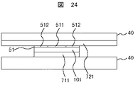
したがって、本発明で望ましい絞込率は2以上、100以下程度、すなわち面積率が1/2〜1/100であるといえる。絞込率が1から2以下となってもよいが、絞込率が1から2では、図22のような複数の電流絞込層導電部の配置された構成では絞込率の制御が困難になる。絞込率が上記の好ましい範囲内で、かつ2近傍の構成は図24に示すような単一の絞込層導電部を有した構成が望ましい。
【0043】
図24は絞込率が低い本発明の磁気ヘッドの構成例である。一対の電極40の間に、下部導電性ギャップ膜711、巨大磁気抵抗効果積層膜101、電流絞込層51、上部導電性ギャップ膜721、を配置してなる。電流絞込層51は、単一の電流絞込層導電部511と、電流絞込層非導電部512からなり、電流絞込層導電部511に感知電流が流れて磁気ヘッドとして機能する。電流絞込層導電部511は、さまざまな作製方法で作ることが可能だが、フォトレジスト工程を用いてトラック幅より狭いパターンとして作製することが望ましい。
(実施例2)
本実施例の巨大磁気抵抗効果積層膜を構成する薄膜は高周波マグネトロンスパッタリング装置により以下のように作製した。アルゴン1から6ミリトールの雰囲気中にて、厚さ1ミリのセラミックス基板に以下の材料を順次積層して作製した。スパッタリングターゲットとしてタンタル、ニッケル−20at%鉄合金、銅、コバルト、MnPt、ルテニウム、アルミナ、MnIr、アルミニウムの各ターゲットを用いた。Coターゲット上には、FeおよびNiの1センチ角のチップを適宜配置して組成を調整した。RuおよびCuターゲット上にはAu、Ag、Ptなどのチップを適宜配置して合金薄膜を形成した。同様にアルミナターゲット上にはAu、Ag、Pt、Alなどのチップを適宜配置してグラニュラー薄膜を形成した。積層膜は、各ターゲットを配置したカソードに各々高周波電力を印加して装置内にプラズマを発生させておき、各カソードごとに配置されたシャッターを一つずつ開閉して順次各層を形成した。膜形成時には永久磁石を用いて基板に平行におよそ80エルステッドの磁界を印加して、一軸異方性をもたせた。
【0044】
形成した膜を、真空中、磁場中で270℃、3時間の熱処理を行ってMnPt反強磁性膜を相変態させ、室温での磁気抵抗を測定して評価した。MnPt以外の反強磁性膜を併用する場合には異なる温度の着磁熱処理を併用した。また、硬磁性膜を用いた構成では熱処理後に室温で着磁処理を行った。基体上の素子の形成はフォトレジスト工程によってパターニングした。その後、基体はスライダー加工し、磁気記録装置に搭載した。
【0045】
以下に本発明の更なる具体的な実施例を、図を追って説明する。
図1は本発明の磁気センサの原理の一つを示す構成例である。磁気ヘッドとして応用した場合に磁気媒体に対向する対向面から眺めた模式図で示した。基体上50に下部磁気シールド35、下部導電性ギャップ膜711を形成し、その上に、巨大磁気抵抗効果積層膜101、電流絞込層51、単磁区化強磁性層45が形成されてなり、さらに上部導電性ギャップ膜721、上部磁気シールド36を形成して、再生信号を検出する再生ギャップ43を形成してなる。絶縁膜75は巨大磁気抵抗効果積層膜101に膜厚方向に電流を印加する領域を定義し、その領域の周りに配置される。同様に本図では巨大磁気抵抗効果積層膜101、電流絞込層51、および単磁区化強磁性膜45を所定のほぼ形状にパターニングして、電流の流れる領域及び磁気的な動作領域を規定してなる。本図では単磁区化強磁性層45を巨大磁気抵抗積層膜101に積層配置の形態で構成し、巨大磁気抵抗効果積層膜101のセンサ部を磁区制御して安定した出力を得る構造となっている。
【0046】
本実施例で、自由層もしくは軟磁性自由層とは、外部磁場によって磁化回転する軟磁性膜を意味している。同様に、固定層もしくは強磁性固定層とは、感知すべき磁界に対して、実質的に磁化が固定されている強磁性層を意味する。固定層の磁化を固定するための手段としては反強磁性膜を用いるが、硬磁性膜すなわち比較的大きな磁界が加わらない限り磁化が変化しない材料で代替することもできる。スペキュラー効果やあるいはSynthetic ferrimagnetと呼ばれるような強磁性固定層を多層構造にする構造も提唱されている。
【0047】
本図での単磁区化強磁性層45は、強磁性層412、反強磁性層413を積層して反強磁性層413と強磁性層412の接合界面で交換結合磁界により強磁性層412の磁化が所定方向、特にトラック幅方向に実質的に固定もしくは残留してなる構成を有するが、これらを別の構成で同等の効果を得ることもできる。例えば単磁区化強磁性層45を硬磁性膜から構成してもよい。本実施例では、巨大磁気抵抗効果積層膜101は、下地膜14、反強磁性膜11、強磁性固定層15、非磁性中間層である非磁性導電層12、軟磁性自由層13が連続して形成された構造を備えている。図1の構成例では、強磁性固定層15は単層であるが、積層構成としても良い。ここで、強磁性固定層15をRuなどの磁気的な反平行結合を発現する層を介して積層した強磁性層/反平行結合層/強磁性層とした構造にすると、実質的な静磁界の発生がゼロに近づくため望ましい。
【0048】
またここで軟磁性自由層13は単層の磁性体として図示したが、2層以上の積層体から形成しても何ら本発明の趣旨に反するものではない。特に、非磁性中間層である非磁性導電層12に近い側をCo合金、反対側をNiFe合金から形成すると、軟磁気特性と高い抵抗変化率を両立できてよい。また巨大磁気抵抗効果積層膜101に適切な保護膜などをさらに積層してもよいが、以下に述べる電流絞込層の効果を阻害しないように、数ナノメートル以下で、導電性のよい物を用いることが望ましい。
【0049】
本図の構成では、膜厚方向に印加する感知電流は、図示されていない電極から磁気シールド36、上部導電性ギャップ膜721、保護膜兼電極膜37、単磁区化強磁性膜45などの経路を経て、電流絞込層51を介し、巨大磁気抵抗効果積層膜101中を通じる。さらに下部導電性ギャップ膜711、下部磁気シールド35などの経路を経て、図示されていない電極へ抜けて、膜厚方向の電流経路を実現する。当然、電流の経路が正負逆としたり、他に電極構成を設けて磁気シールド部を迂回したりしても本発明の主旨に反するものではない。本発明の主旨は巨大磁気抵抗効果積層膜101中の電流の通電経路にある。図中、矢印53に電流の通電経路を概念的に示した。
【0050】
本発明において電流絞込層とは、先に述べた如く、基本的に、一対の電極を経由して磁気抵抗効果膜を電流が膜厚方向に通電する通電経路中に、通電経路を横断する構造で配置される層状の構造体であって、
上記層状構造体の面内で、非導電体からなる非導電層中に導電体からなる部分、例えば穴状部分からなる導電部が膜厚方向に埋めこまれた構造を有する層状構造体であって、
上記構造により、膜厚方向、すなわち面に垂直に流れる電流の経路を、電流絞込層内部の導電部分に限定して絞込む効果があり、磁気抵抗効果膜と近接して積層することによって、この絞込み効果を磁気抵抗効果膜の電気抵抗の実質的増幅として機能させる構造体、である。
【0051】
本実施例でさらに具体的に示すと、電流絞込層51は電流絞込層導電部511および電流絞込層非導電部512からなる。電流絞込層導電部511は、例えばAu,Cu、Alなどの導電性の高い金属の粒子からなり、電流絞込層非導電部512より極端に低い電気抵抗率を示す領域で、電流絞込層51の面積の所定の割合、例えば1/2から1/100を占めるよう形成されてなる。膜厚方向電流は、上部磁気シールド36および上部導電性ギャップ膜712中では広い面積を流れているが、非導電膜75によって巨大磁気抵抗効果積層膜101部に絞られて通電する。電流絞込層51がない場合、巨大磁気抵抗効果積層膜101中での膜厚方向電流は巨大磁気抵抗効果積層膜101の面内でおおよそ均一で流れるはずである。しかしながら本発明の構成では電流絞込層51の存在により、膜厚方向電流は電流絞込層導電部511の部分に集中し、膜厚方向電流の流れる面積を巨大磁気抵抗積層膜101の面積に対しての所定の割合、すなわち電流絞込層導電部511の面積率に応じた割合で絞ることができる。
【0052】
電流絞込層51を通過した電流は巨大磁気抵抗効果積層膜101に通電する。膜厚方向電流は電流絞込層511から離れるとともに電流絞込層導電部511の面内のサイズより広がって通電するが、本発明の構成では電流絞込層51と巨大磁気抵抗積層膜101中の非磁性中間層である非磁性導電層12との距離を、例えば5ナノメートル以下、特に3ナノメートル以下に低減してなるので、膜厚方向電流の広がりが小さい状態で非磁性導電層12に通電する事ができる。ここで、各層間の距離、は各層の互いに近い側の界面間の距離として定義している。
【0053】
したがって、巨大磁気抵抗の膜厚方向電流による磁気抵抗効果を、巨大磁気抵抗効果積層膜101の面積から得られるよりも、高い電気抵抗かつ高い抵抗変化率で再生出力を得ることができる。電流絞込層51と巨大磁気抵抗積層膜101中の非磁性中間層である非磁性導電層12との距離を上記のように小さくするには、軟磁性自由層13の厚さを5ナノメートル以下、特に3ナノメートル以下とすることで実現できる。また、本図では図示していないが、軟磁性自由層13と電流絞込層51の間に非磁性分離層を形成すると、軟磁性自由層13の磁気的な特性を良好に保つ効果、特に磁歪の制御および保磁力の低減に効果がある。しかしながら、上記非磁性分離層の厚さも電流絞込層51と巨大磁気抵抗積層膜101中の非磁性中間層である非磁性導電層12との距離に加算されるので、上記非磁性分離層は極力薄く、特に1ナノメートル以下であることが望ましい。同様に軟磁性自由層13と非磁性分離層の厚さの合計が5ナノメートル以下、特に3ナノメートル以下が望ましい。
【0054】
さらに、本発明の構成によれば膜厚方向電流は矢印53に示したように、非磁性中間層である非磁性導電層12を通電後に広がっていくが、このため、反強磁性膜11を通電する際には非磁性導電層12の通電時より数倍の領域に広がり、反強磁性膜11の膜厚方向の電気抵抗への寄与を、おおよそ上記広がりのマイナス二乗に比例して低減することができる。巨大磁気抵抗効果積層膜101を通電した電流は、広い面積で下部非磁性導電性ギャップ膜711および下部磁気シールド35を通じて感知電流として機能するのである。
【0055】
電流絞込層51の電流絞込層導電部511は電流絞込層絶縁部512の中にドット状あるいは島状の形態で分布して形成されてなり、電流絞込層51中で所定の面積率(面積率の定義については既述)、例えば1/100〜1/2の存在比率を有する。電流絞込層導電部511のサイズは、非磁性中間層である非磁性導電層12までの距離および軟磁性自由層13の厚さより数倍以上大きく形成するとよい。これは、電流絞込層51からの電流の広がりが非磁性導電層に達するまでは比較的無視できるように、幾何学的必要性で決定される。同様に電流絞込層導電部511のサイズは感知すべき磁気記録単位より十分小さく作製する。すなわち、電流絞込層導電部511のサイズが感知すべき磁気記録単位、特にトラック幅や素子高さ、素子感応部のサイズと同程度の大きさから数分の一程度の大きさの場合、素子感応部に含まれる電流絞込層導電部511の個数は離散的となり、安定した特性の素子を生産することが困難であるからである。
【0056】
電流絞込層51の構成は、上述の構成を含め、様々な作製法、および構成によって実現が可能である。電流絞込層導電部511をCu、Agなどの金属の島状組織で形成し、電流絞込層非導電部512である酸化アルミニウムのマトリクスで周囲を埋めた構造としてもよい。あるいは、スクリーニング層51をアルミニウムとCu、Ag 、Au、Ptなどの混合薄膜で形成し、薄膜形成後に熱処理によって金属粒子を析出される手法で形成してもよい。電流絞込層51をアルミニウムとCu、Ag 、Au、Ptなどの島状組織との混合薄膜で形成し、薄膜形成後に酸化処理によってアルミナ中に未酸化の金属粒子が残存する手法で形成してもよい。
【0057】
ここでは、特に、図4に示したような手法で作製した構成が望ましい。具体的には、Alの層を形成し、Cu、Auなどからなる島状組織を形成し、上記島状組織をマスクにしてAl層を部分的に酸化し、最終的にAlからなる導電部分と、Al−Oからなる非導電部分を所定の面積率で作製した構成である。このような島状組織などの自己配列組織を内包した構成が本発明に利用することができる。
【0058】
すなわち、本発明の主要な原理の一つは、面内の狭い面積に部分的に導電性を有する電流絞込層51を非磁性導電層12に近接して配置し、膜厚方向電流を巨大磁気抵抗効果積層膜101に印可することで、非磁性導電層12に通電する膜厚方向電流を所定の面積の中で絞り、高い素子抵抗と高い抵抗変化率を実現するとともに、反強磁性膜11による素子抵抗の増加と抵抗変化率の低減を防止することができるというところにある。
【0059】
上記の効果は、当然、反強磁性膜などの高抵抗膜が電流絞込層51の上部側、下部側のいずれに配置されていても同様の効果があるのに加えて、反強磁性膜などの高抵抗膜が電流絞込層51の上部側、下部側の双方に配置されていても同様に効果的である。したがって本発明では電流絞込層の上下に反強磁性膜が積層された巨大磁気抵抗効果センサを実現することができる。図1に示したような磁区制御のための反強磁性膜46と、巨大磁気抵抗効果積層膜101の反強磁性膜11が電流絞込層51の上下にそれぞれ配置された構造で高い抵抗変化率を有するセンサを実現できるのである。
【0060】
次に本発明の電流絞込層の積層構成とそのサイズについて説明する。図10はサイズの異なるスクリーニング層による電流絞込の電流分布を示した図である。用いたデータは、円柱(z−r)座標系を仮定して計算した結果である。zおよびr方向についてそれぞれz方向に1ナノメートル、r方向に1ナノメートルのサイズの40×40のセルに分割した導体中にr=0を中心にした円形の穴(導電部)を有する絶縁部(図中太線の形状)を配置してZ方向に電圧を印可し、電流分布を算出した。すなわち、個々の影響が十分無視できる程度に距離が離れて独立であるとして扱える電流絞込層導電部の電流分布を計算機実験で確かめたものである。z軸方向の電流成分の等高線図として示した。図中太線でしめした非導電部によって電流の経路は限定され、非導電部のない所定のサイズの穴状である導電部を伝導する。導電部の穴を通過する前および後の電流はr方向に広がりながら導電する様子が図からわかるが、その広がり方の程度は導電部のサイズによって異なっている。導電部の直径が6ナノメートルと小さいと、穴の位置からz方向に電流の等高線は、1ナノメートルに数本存在し、すなわち密であって、電流が急激に拡散、減少していることがわかる。導電部の直径が大きい場合の電流分布を見ると、導電部の直径とともに次第に等高線の間隔は広がり、導電部のサイズが大きいとz方向に穴部から離れても電流が広がりが小さいことがわかる。
【0061】
図11に導電部のサイズを変えた時の、z方向離れた位置での電流密度分布を示した。電流密度は導電部の中心の電流密度を100として規格化して示してある。図中点線で導電部の端部を示してあるが、z位置が0、すなわち導電部直下、または直上、では穴よりr位置が大きい部分では絶縁部によって電流がゼロになっており、また、導電部の端部で電流密度が高くなっている。これは非伝導部を回り込んだ電流がもっとも短いバスを通るために穴の端部に集中するためである。z位置が0より大きい、すなわちz方向に導電部の穴から離れた位置では、電流密度は穴部の中心で高く、r位置が大きくなるほど減衰していることがわかる。
【0062】
導電部のサイズを変えた場合で比較すると、導電部の直径が6ナノメートルではzが2、4、6と増えるとr=0近傍の電流密度が急激に低下し、かつ導電部直径より外、すなわち、図中点線より右側で電流密度が裾を持ち、zが大きいほど広がった電流分布をしていることがわかる。一方で、導電部直径が24ナノメートルと大きい場合には、zが2、4、6と増えた場合のr=0近傍の電流密度の低下は、導電部のサイズが小さい場合に比べて極めて小さく、比較すると導電部のサイズが大きいほど電流分布の広がりが小さい結果になった。
【0063】
図12は導電部の直径を変えたときのz位置離れた部分の電流効率を示した図である。ここで電流効率は、z位置離れた部分で導電部相当の面積に流れる電流の総量を導電部(z=0)を通る電流の総量を1として規格化した値である。すなわち、導電部の穴状の部分によって絞られた電流がz位置離れた部分でどの程度絞られているかの指標と言って良い。導電部の直径が6ナノメートルの場合、zが1ナノメートル離れた場所の電流量は導電部の1に対して0.6程度まで急激に低下しており、導電部のサイズが小さいとわずか1ナノメートル離れただけで電流絞込の効果が4割失われることを示している。これに対して導電部の直径が48ナノメートルの場合、電流量はzに対して比較的緩やかに減衰し、例えばz位置が4ナノメートル離れて電流量は全体のおよそ0.8、すなわち絞込効果の8割を得ることができる。このような電流絞込効果のサイズ依存性は磁気抵抗効果素子の特性に直接影響を与える。
【0064】
図14は電流効率と再生素子の特性を計算した結果である。ここで電流の絞込率βを導電部の面積率の逆数として定義し、素子面積SMR、一個の導電部の面積をs0、導電部、巨大磁気抵抗部および反強磁性膜の電気抵抗率をρ0、ρMR、ρAF、同様に厚さをそれぞれt0、tMR、tAF、とし、以下の算出を行った。本発明のスクリーン層を用いない場合、素子抵抗R1および抵抗変化量ΔR1は下記のようになる。
R1=ρMR・tMR/SMR+ρAF・tAF/SMR、
ΔR1=MR・ρMR・tMR/SMR
ここでMRは巨大磁気抵抗部の抵抗変化率である。一方で本発明のスクリーン層を用いた場合の素子抵抗R0および抵抗変化量ΔR0は、
R0=ρ0・t0・β/S+ρMR・tMR。・β・γ/SMR+ρAF・tAF/SMR、
ΔR0=MR・ρMR・tMR。・β・γ/SMR
βは絞込率、γは電流効率である。
【0065】
以上の式に、ρ0=30×10−8Ωm、ρMR=30×10−8Ωm、ρAF=180×10−8Ωm、同様に厚さをそれぞれt0=2×10⁻⁹m、tMR=3×10⁻⁹m、tAF=15×10−9m、MR=0.3(30%)、β=100を代入して計算を行った。図13の結果は導電部(穴)の直径が大きいほど素子の抵抗変化率ΔR/Rが大きいことを示しており、さらに導電部のz位置の値が大きくなるほどΔR/Rが低下して導電部の直径が大きくなっても改善しにくいことがわかる。十分高い出力の素子を得るためには、図13においてΔR/Rが2本の点線の間程度に十分に飽和値に近いことが望ましいが、したがって高い出力を得るための素子構造は導電部の直径と導電部のz位置について所定の関係を持つ必要がある。例えばz=2(nm)であれば導電部の直径はおよそ10nm以上あれば良いが、z=6(nm)であれば導電部の直径は30ナノメートル以上必要であることがわかる。一方で導電部の直径は素子サイズからも規制を受ける。
【0066】
図14は素子内の導電部の数と導電部の直径の関係を示した図である。絶縁体によって互いに隔てられた穴状の導電部は、所定のサイズの素子の中に配置され、したがって、(1)素子のサイズより小さく、(2)複数の導電部が独立であるためにその素子面積に対する面積率は1/2以下であり、(3)所定の絞込率βを実現する合計の面積を有する、等の条件によって規定される。図14に示した結果は、素子面積SMR、素子内の導電部数n、絞込率β、導電部直径dについて、
(d/2)2≦SMR/(2π・n・β)
として上記条件を満たす導電部数と導電部直径を示したものである。
【0067】
ここで素子面積としては磁気記録装置の典型的なサイズである0.1μm角を基準に求めた。図14の結果は、絞込率βが大きいほど、また素子内導電部数が大きいほど導電部の直径は小さい必要があることを示しており、仮に絞込率βが2と低い値でも、導電部の直径は60ナノメートル以下であり、通常、導電部の直径は30ナノメートル以下となることがわかる。これにより導電部の直径の最大値が規定され、図13の結果と合わせるとスクリーニング層の導電部のサイズとz方向の配置位置が規定される。
【0068】
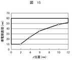
図15は電流絞込層のz方向配置位置と導電部の直径の関係を示した図である。図中太線部内の構成では図13、14で示した条件を満たしており、高い素子出力を得ることが出きる。z位置の値が小さい、すなわち電流絞込層の配置が磁気抵抗部の中核である非磁性中間層に極めて近い2〜3ナノメートル程度であると、導電部の直径が10〜60ナノメートルと広い範囲で高い出力の素子を得ることができる。一方で電流絞込層の配置が非磁性中間層から10ナノメートルと遠い構成では導電部直径が50〜60ナノメートルと大きく導電部で、かつ狭いサイズ領域でしか高い素子出力が得られない。特に作製時のばらつきやマージンを考慮すると、電流絞込層のz位置が2〜6ナノメートルで、導電部のサイズが10〜60ナノメートルであることが望ましいのである。
【0069】
実際に積層膜の厚さや磁気的な特性から、さらに望ましい構成を規定すると、非磁性中間層すなわち非磁性導電層と電流絞込層の間隔が1から3ナノメートルとすることが望ましい。すなわち、巨大磁気抵抗効果が実際に生じている部分は積層構成のうち、非磁性中間層もしくは非磁性導電層と呼ばれる部分でおおよそ2nm程度の厚さのCu層からなり、この層と直接積層した一対の強磁性層との界面が主要な物理現象の現場であるわけだが、強磁性層自体にも、機能を発揮するための所定の厚さがあり、少なくとも1ナノメートル、以上の厚さを要するからである。同様に強磁性膜の厚さが3nmを超えても物理的には余剰部分と言えるからである。以上の理由から、非磁性中間層と電流絞込層の間隔は最小で1ナノメートル必要であり、また、5ナノメートル以下、さらに望ましくは3ナノメートルあれば所定の効果が得られることが規定できるのである。
(実施例3)
図2は本発明の巨大磁気抵抗効果型磁気ヘッドの別の構成例である。本実施例の磁気ヘッドは、電流絞込層の上下に巨大磁気抵抗効果積層膜をそれぞれおよそ対称に配置する構造を特徴とする。磁気ヘッドとして応用した場合に磁気媒体に対向する対向面から眺めた模式図で示した。基体上50に下部磁気シールド35、下部導電性ギャップ膜711を形成し、その上に、巨大磁気抵抗効果積層膜101、電流絞込層51、巨大磁気抵抗効果積層膜101が形成されてなり、さらに上部導電性ギャップ膜721、上部磁気シールド36を形成して、再生信号を検出する再生ギャップ43を形成してなる。絶縁膜75は巨大磁気抵抗効果積層膜101に膜厚方向に電流を印加する領域を定義し、その領域の周りに配置される。
【0070】
同様に本図では巨大磁気抵抗効果積層膜101、電流絞込層51、および単磁区化強磁性膜45を所定のほぼ形状にパターニングして、電流の流れる領域及び磁気的な動作領域を規定してなる。本図では単磁区化強磁性層45を巨大磁気抵抗積層膜101に積層配置の形態で構成し、巨大磁気抵抗効果積層膜101のセンサ部を磁区制御して安定した出力を得る構造となっている。上下の巨大磁気抵抗効果積層膜101は基本的に同様の構成であるが、その磁性膜の積層構成は上下で対象である。すなわち、基板側では下地膜14、反強磁性膜11、強磁性固定層15、非磁性中間層である非磁性導電層12、軟磁性自由層13と構成し、スクリーニング層51を挟んで、さらに軟磁性自由層13、非磁性導電層12、強磁性固定層15、反強磁性膜11、保護膜兼電極膜37を構成してなる。また、磁区制御膜41は、硬磁性膜などからなり、巨大磁気抵抗効果積層膜101の側部、特にトラック幅方向の端部に近接して配置して、巨大磁気抵抗効果積層膜101のセンサ部、すなわち軟磁性自由層13を単磁区化してノイズのない出力を得ることができる。以下、その他の概略は図1と同様である。
(実施例4)
図3は本発明の巨大磁気抵抗効果型磁気ヘッドのまた別の構成例である。対向面に平行な断面図で示した。図は磁気媒体に対向する対向面から眺めた模式図になっている。基体50上に下部磁気シールド35、下部ギャップ膜71を形成し、その上に、巨大磁気抵抗効果積層膜101が形成されてなり、さらに上部ギャップ膜72、上部磁気シールド36を形成して、再生信号を検出する再生ギャップ43を形成してなる。電極40は、巨大磁気抵抗効果積層膜10のトラック幅方向の両端部に接触して配置し、感知電流の印可と電気抵抗の変化の検出を行う。電極40の形成方法およびその形状は、ここではいわゆるリフトオフ法によって作製した構造で記述してあるが他にさまざまな方法が利用できる。
【0071】
巨大磁気抵抗効果積層膜101は、図1と同様に図3では以下の構成例のような構造を有する。巨大磁気抵抗効果積層膜101は下地膜14、反強磁性膜11、強磁性固定層15、非磁性中間層である非磁性導電層12、軟磁性自由層13を連続して形成してなる。この構成例では強磁性固定層15は第一の強磁性膜151と第二の強磁性膜152、および反平行結合膜154の積層体からなる。反平行結合膜154は第一の強磁性膜151と第二の強磁性膜152の磁化を互いに反平行に配列させる交換結合を印加して、強磁性固定層の実質的な磁化の量を第一の強磁性膜151と第二の強磁性膜152の磁化量の差分に制御する効果がある。ここで強磁性固定層15を単層の磁性体から形成したり、2層や4層以上の積層体から形成しても何ら本発明の趣旨に反するものではない。またここで軟磁性自由層13は第一の自由層軟磁性膜および第二の自由層軟磁性膜の積層体からなるが軟磁性自由層13を単層の磁性体から形成したり、2層以上の積層体から形成しても何ら本発明の趣旨に反するものではない。特に、非磁性導電層12に近い側をCo合金、反対側をNiFe合金から形成すると、軟磁気特性と高い抵抗変化率を両立できてよい。
【0072】
本図の構成では、膜厚方向に印加する感知電流は、図示されていない電極から磁気シールド36、上部導電性ギャップ膜721、保護膜兼電極膜37などの経路を経て、電流絞込層51を介し、巨大磁気抵抗効果積層膜101中を通じる。さらに下部導電性ギャップ膜711、下部磁気シールド35などの経路を経て、図示されていない電極へ抜けて、膜厚方向の電流経路を実現する。当然、電流の経路が正負逆としたり、他に電極構成を設けて磁気シールド部を迂回したりしても本発明の主旨に反するものではない。
【0073】
本発明の主旨は巨大磁気抵抗効果積層膜101中の電流の通電経路にある。図中、矢印53に電流の通電経路を概略的に示した。電流絞込層51は電流絞込層導電部511および電流絞込層非導電部512からなる。電流絞込層導電部511は、例えばAu、Cu、Alなどの導電性の高い金属の粒子からなり、電流絞込層非導電部512より極端に低い電気抵抗率を示す領域で、電流絞込層51の面積の所定の割合、例えば1/2から1/100を占めるよう形成されてなる。膜厚方向電流は、上部磁気シールド36および上部導電性ギャップ膜712中では広い面積を流れているが、非導電膜75によって巨大磁気抵抗効果積層膜101部に絞られて通電する。
【0074】
以下、概略は図1の場合と同様であり、図3において異なるのは磁区制御の構成である。図3の構成例では、磁区制御膜41は、硬磁性膜などからなり、巨大磁気抵抗効果積層膜101の側部、特にトラック幅方向の端部に近接して配置して、巨大磁気抵抗効果積層膜101のセンサ部、すなわち軟磁性自由層13を単磁区化してノイズのない出力を得ることができる。逆に巨大磁気抵抗効果積層膜101に全面に積層した磁区制御構造は配置しない構成となっている。
(実施例5)
図4は本発明の巨大磁気抵抗効果型磁気ヘッドの電流絞込層の構成と作製方法の第一例を示した図である。巨大磁気抵抗効果積層膜101を形成し、その表面上にAlの膜を1〜数ナノメートル程度の形成する。ここではAlを例としたが、代換材料としては相応の共有結合性化合物を形成しやすく、伝導性の高い金属が望ましい。次にAl層上に島状の粒組織を形成する。粒組織はCu、Auなどの化合物を形成しにくい、貴金属などが望ましく、形成条件を適切にすることで連続膜ではなく所定のサイズと面積率の島状組織を形成せしめる。次に上記構造の表面を酸素雰囲気に暴露し、Al層の露出部分を酸化する。酸素以外の化合物形成ガスを用いてもよいし、ガスでなくプラズマに暴露してもよいが、Alなどと化合して絶縁性の化合物を形成する雰囲気に暴露することが肝要である。
【0075】
島状組織に覆われていない部分のAl層を、上記暴露によって非導電化合物、ここではAl−Oに反応形成物層に形成し、保護膜、電極層などをさらに積層してスクリーニング層51を形成することができる。上記スクリーニング層51の作製工程は、真空薄膜形成装置チャンバー内で行い、大気開放されずに、別室で酸素暴露するなどの方法作製することが望ましい。図示したように、酸化したAl−O部がスクリーニング層絶縁部512、Cu、Auなどの島状組織酸の粒子が接した非酸化Al部分がスクリーニング層導電部511となる。
(実施例6)
図5は本発明の巨大磁気抵抗効果型磁気ヘッドの電流絞込層の構成と作製方法の第二例を示した図である。巨大磁気抵抗効果積層膜101を形成し、その表面上にAu、Cu、Agなどの膜を1〜数ナノメートル程度の形成する。ここではAu、Cu、Agを例としたが、化合物を形成しにくい、伝導性の高い金属、すなわち貴金属などが望ましい。次に上記Au、Cu、Agの層上にAlなどからなる島状の粒組織を形成する。粒組織はAlの代換材料としては相応の共有結合性化合物を形成しやすい材料が望ましい。粒組織は形成条件を適切にすることで連続膜ではなく所定のサイズと面積率の島状組織を形成せしめる。
【0076】
次に上記構造の表面を酸素雰囲気に暴露し、粒組織を酸化する。酸素以外の化合物形成ガスを用いてもよいし、ガスでなくプラズマに暴露してもよいが、Alなどと化合して絶縁性の化合物を形成する雰囲気に暴露することが肝要である。Alなどからなる粒組織を、上記暴露によって非導電化合物、ここではAl−Oに反応形成物層に形成し、保護膜、電極層などをさらに積層してスクリーニング層51を形成することができる。上記スクリーニング層51の作製工程は、真空薄膜形成装置チャンバー内で行い、大気開放されずに、別室で酸素暴露するなどの方法作製することが望ましい。ここで酸化したAl−O部がスクリーニング層絶縁部512、Al−Oが被覆していない部分およびそれに接したAu、Cu、Agなどの島状組織酸の粒子が接した非酸化Al部分が電流絞込層導電部511となる。
【0077】
これらの導電部および非導電部は、作製手段の如何によらずその形状、サイズと配置によって電流絞込層として機能するから、図10から図15で記述した導電部および非導電部の適したサイズとすると本発明の効果を発揮することができる。具体的には導電部、すなわち非酸化Alもしくは金属粒子部分が5ナノメートルから50ナノメートル、とし、非磁性中間層から1から5、もしくは1〜3ナノメートルの所定の位置に配置するとよいのである。なお、上記導電部を構成する金属微粒子の平均粒径が5ナノメートル未満では、電流密度が大きくなり過ぎて不適である。また、50ナノメートルを越えると、電流の絞込率が低下して不適となる。
(実施例7)
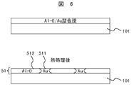
図6は本発明の巨大磁気抵抗効果型磁気ヘッドの電流絞込層の構成と作製方法の第三例を示した図である。巨大磁気抵抗効果積層膜101を形成し、その表面上にAl−OとAuの混合膜を1〜数ナノメートル程度の形成する。ここではAuを例としたが、化合物を形成しにくい、伝導性の高い金属、すなわちAu、Cu、Agなどの貴金属などが望ましい。同様にAl−Oの代換材料としては相応の共有結合性化合物材料が望ましい。上記構造にさらに保護膜や導電膜などを形成した後、次に上記構造を所定の温度と時間で熱処理する。熱処理条件、特に温度と時間、と、混合膜のAl−OとAuの混合組成、および膜形成条件を適切にすることで、混合膜から所定のサイズと面積率の導電性粒子の島状組織を形成せしめて電流絞込層51を形成することができる。上記電流絞込層51の作製工程は、真空薄膜形成装置チャンバー内で行い、保護膜等を形成することが望ましい。ただし熱処理は大気開放した後に別装置でを行うことができる。ここでAl−O部が電流絞込層非導電部512、析出したAuなどの島状組織の粒子部分が電流絞込層導電部511となる。
(実施例8)
図7は本発明の巨大磁気抵抗効果型磁気ヘッドの電流絞込層の構成と作製方法の第四例を示した図である。巨大磁気抵抗効果積層膜101を形成し、その表面上にAu、Cu、Ruなどの膜を1〜数ナノメートル程度の形成する。ここではAu、Cu、Ruを例としたが、化合物を形成しにくい、伝導性の高い金属、すなわち貴金属などが望ましい。次に上記Au、Cu、Ruなどの層上にAl―Auなどからなる層を形成する。上記Al−Au層は、Alの代換材料としては相応の共有結合性化合物を形成しやすい材料とAuの代わりに化合物を形成しにくい、伝導性の高い金属、すなわち貴金属などで置換できる。
【0078】
次に上記構造の表面を酸素雰囲気に暴露し、Al−Au層を酸化する。酸素以外の化合物形成ガスを用いてもよいし、ガスでなくプラズマに暴露してもよいが、Alなどと化合して非導電性の化合物を形成する雰囲気に暴露することが肝要である。上記酸化処理によって、Al―Au層を絶縁化合物、ここではAl−Oと、Auの粒子状非反応部を形成し、保護膜、電極層などをさらに積層して電流絞込層51を形成することができる。上記電流絞込層51の作製工程は、真空薄膜形成装置チャンバー内で行い、大気開放されずに、別室で酸素暴露するなどの方法作製することが望ましい。ここで酸化したAl−O部が電流絞込層非導電部512、Auなどの非反応部の島状組織が電流絞込層導電部511となる。
(実施例9)
図8は本発明の巨大磁気抵抗効果型磁気ヘッドの電流絞込層の構成と、塗布粒子による作製方法の第一例を示した図である。巨大磁気抵抗効果積層膜101を形成し、その表面上にAu、Cu、Ruなど貴金属の膜を1〜数ナノメートル程度形成する。ここではAu、Cu、Ruを例としたが、化合物を形成しにくい伝導性の高い金属(例えば貴金属など)が望ましい。次に上記Au、Cu、Ruなどの層上にAuなどの粒子を塗布する。Au以外の粒子でもよいが、貴金属が望ましい。Au粒子は有機溶媒中にミセルなどの形でコロイド粒子となっているものを、適宜に希釈し、回転塗布することで膜上に適切な密度で形成できる。
【0079】
別の塗布手段としては、水などの液体表面上に、粒子を含有した溶液を液体表面に分子膜状に分散させ、しかる後にこの分散膜を基板上に付着せしめることもできる。上記のような粒子の塗布後、適宜、熱処理やプラズマ処理を行って、粒子から余剰の有機分子などを除去することが望ましい。上記粒子を配置した後に、Al−Oなどからなる絶縁性薄膜を形成すると、粒子がマスクとなって粒子の存在密度とサイズに対応した穴部を有したAl−O層が形成できる。次にAu粒子を方位性ミリングやクラスタービームなどによって除去し、保護膜や電極膜を形成して電流絞込層51を形成できる。
(実施例10)
実施例8では粒子を除去する工程を含めたが、粒子を残存させることも可能である。巨大磁気抵抗効果積層膜101の上に形成されたAl−O層が電流絞込層絶縁部512となり、Al−O層の穴に該当する部分が電流絞込層導電部511となる。図9は本実施例での電流絞込層の構成と、塗布粒子による作製方法の第二例を示した図である。巨大磁気抵抗効果積層膜101を形成し、その表面上にAu、Cu、Ruなど貴金属の膜を1〜数ナノメートル程度の形成する。ここではAu、Cu、Ruを例としたが、化合物を形成しにくい、伝導性の高い金属、すなわち貴金属などが望ましい。
【0080】
次に上記Au、Cu、Ruなどの層上にAuなどの粒子を塗布する。Au以外の粒子でもよいが、貴金属が望ましい。Au粒子は有機溶媒中にミセルなどの形でコロイド粒子となっているものを、適宜に希釈し、回転塗布することで膜上に適切な密度で形成できる。塗布後、適宜、熱処理やプラズマ処理を行って、粒子から余剰の有機分子などを除去することが望ましい。上記粒子を配置した後に、Alなどからなる、非導電性化合物を作りやすい金属などを形成すると、粒子がマスクとなって粒子の存在密度とサイズに対応した穴部を有したAl層が形成できる。
【0081】
次に上記構造の表面を酸素雰囲気に暴露し、Al−Au層を酸化する。酸素以外の化合物形成ガスを用いてもよいし、ガスでなくプラズマに暴露してもよいが、Alなどと化合して絶縁性の化合物を形成する雰囲気に暴露することが肝要である。上記酸化処理によって、Al―Au層を絶縁化合物、ここではAl−Oと、Auの粒子状非反応部を形成し、保護膜、電極層などをさらに積層して電流絞込層51を形成することができる。ここでは粒子を除去しない構成例を示したが、図8の例で示したように次にAu粒子を方位性ミリングやクラスタービームなどによって除去することも可能である。巨大磁気抵抗効果積層膜101の上に形成されたAl−O層が電流絞込層絶縁部512となり、Al−O層の穴に該当する部分が電流絞込層導電部511となる。
(実施例11)
図16は本発明の磁気抵抗効果素子による磁気センサーを搭載した磁気ヘッドの構成例の概念図である。基体50上に巨大磁気抵抗効果積層膜101、下部磁気シールド35、上部磁気シールド36、下部磁気コア84、コイル42、上部コア83を形成してなり、対向面63を形成してなる。磁区制御膜等は巨大磁気抵抗効果積層膜101の近傍に配置されるが、省略し、図中に示していない。本図では個別に上部シールドと下部コアとを形成した構造になっているが、上部シールドが下部コアを兼ねた構造としても本発明の主旨を損なうものではない。下部磁気コア84、コイル42、上部磁気コア83は記録ヘッドを構成し、電磁誘導効果によって発生する磁界を対抗面63の記録ギャップから発生して磁気ディスク上の記録媒体に記録する。電極40は巨大磁気抵抗効果積層膜101の上下に配置して巨大磁気抵抗効果積層膜101の膜厚方向に電流を印加する。
(実施例12)
図17は本発明の磁気記録再生装置の構成例である。磁気的に情報を記録する記録媒体91を保持するディスク95をスピンドルモーター93にて回転させ、アクチュエーター92によってヘッドスライダー90をディスク95のトラック上に誘導する。即ち磁気ディスク装置においてはヘッドスライダー90上に形成した再生ヘッド、及び記録ヘッドがこの機構に依ってディスク95上の所定の記録位置に近接して相対運動し、信号を順次書き込み、及び読み取るのである。アクチュエーター92はロータリーアクチュエーターであることが望ましい。記録信号は信号処理系94を通じて記録ヘッドにて媒体上に記録し、再生ヘッドの出力を、信号処理系94を経て信号として得る。さらに再生ヘッドを所望の記録トラック上へ移動せしめるに際して、本再生ヘッドからの高感度な出力を用いてトラック上の位置を検出し、アクチュエーターを制御して、ヘッドスライダーの位置決めを行うことができる。本図ではヘッドスライダー90、ディスク95を各1個示したが、これらは複数であっても構わない。またディスク95は両面に記録媒体91を有して情報を記録してもよい。情報の記録がディスク両面の場合ヘッドスライダー90はディスクの両面に配置する。
【0082】
上述したような構成について、本発明の磁気ヘッドおよびこれを搭載した磁気記録再生装置を試験した結果、充分な出力と、良好なバイアス特性を示し、また動作の信頼性も良好であった。
【0083】
【発明の効果】
以上詳述したように、本発明によれば安定した特性と、出力の高い磁気センサと、これを用いた磁気ヘッドが得られ、特に高い記録密度において良好な再生出力を有する磁気ヘッドおよび高密度磁気記録再生装置を得ることができる。
【図面の簡単な説明】
【図1】本発明の巨大磁気抵抗効果型磁気ヘッドの構成例である。
【図2】本発明の巨大磁気抵抗効果型磁気ヘッドの別の構成例である。
【図3】本発明の巨大磁気抵抗効果型磁気ヘッドのまた別の構成例である。
【図4】本発明の巨大磁気抵抗効果型磁気ヘッドのスクリーニング層の構成と作製方法の第一例を示した図である。
【図5】本発明の巨大磁気抵抗効果型磁気ヘッドのスクリーニング層の構成と作製方法の第二例を示した図である。
【図6】本発明の巨大磁気抵抗効果型磁気ヘッドのスクリーニング層の構成と作製方法の第三例を示した図である。
【図7】本発明の巨大磁気抵抗効果型磁気ヘッドのスクリーニング層の構成と作製方法の第四例を示した図である。
【図8】本発明の巨大磁気抵抗効果型磁気ヘッドのスクリーニング層の構成と、塗布粒子による作製方法の第一例を示した図である。
【図9】本発明の巨大磁気抵抗効果型磁気ヘッドのスクリーニング層の構成と、塗布粒子による作製方法の第二例を示した図である。
【図10】サイズの異なるスクリーニング層による電流絞込の電流分布を示した図である。
【図11】導電部のサイズを変えた時の、z方向離れた位置での電流密度分布を示した図である。
【図12】導電部の直径を変えたときのz位置離れた部分の電流効率を示した図である。
【図13】電流効率と再生素子の特性の関係を示した図である。
【図14】本発明の素子内の導電部の数と導電部の直径の関係を示した図である。
【図15】スクリーニング層のz方向配置位置と導電部の直径の関係を示した図である
【図16】本発明の磁気抵抗効果素子による磁気センサーを搭載した磁気ヘッドの構成例の概略図である。
【図17】本発明の磁気記録再生装置の構成例である。
【図18】本発明の磁気ヘッドの、電流絞込層の配置の例を示した図である。
【図19】本発明の磁気ヘッドの、電流絞込層の配置の別の例を示した図である。
【図20】本発明の磁気ヘッドの電流絞込層を含んだ巨大磁気抵抗効果膜の構成例である。
【図21】本発明の磁気ヘッドの電流絞込層を含んだ巨大磁気抵抗効果膜の別の構成例である。
【図22】本発明の電流絞込層の概略図である。
【図23】本発明の電流絞込の効果を示す概算図である。
【図24】絞込み率が低い本発明の磁気ヘッドの構成例である。
【符号の説明】
101…巨大磁気抵抗効果積層膜、11…反強磁性膜、12…非磁性中間層である非磁性導電層、13…軟磁性自由層、14…下地膜、15… 強磁性固定層、151…第一の強磁性膜、152…第二の強磁性膜、154…反平行結合層、35…下部磁気シールド、36…上部磁気シールド、37…保護膜兼電極膜、40…電極、41…磁区制御膜、411…非磁性分離層、412…強磁性層、413…反強磁性層、414…硬磁性層、415…結合層、42…コイル、43…再生ギャップ、44…記録トラック、45…単磁区化強磁性層、46…反強磁性膜、47…電流の経路、50…基体、51…電流絞込層、511…電流絞込層導電部、512…電流絞込層層非導電部、53…電流経路、63…対向面、64…漏洩磁界、711…下部導電性ギャップ膜、721…上部導電性ギャップ膜、7…非導電膜、83…上部磁気コア、84…下部磁気コア、90…ヘッドスライダー、91…記録媒体、92…アクチュエーター、93…スピンドル、94…信号処理系、95…磁気ディスク。[0001]
TECHNICAL FIELD OF THE INVENTION
The present invention relates to a magnetic head used in a magnetic recording / reproducing device, a method of manufacturing the same, and a method of narrowing down the current of the magnetic head.
[0002]
[Prior art]
Japanese Patent Application Laid-Open No. 7-73416 describes an MR read transducer in which an exchange layer is adjacent to a soft active layer. Japanese Patent Application Laid-Open No. 7-169006 describes a spin valve sensor using an antiferromagnetic coupling film. JP-A-10-173252 describes a magnetoresistive sensor in which high-resistance magnetic layers are stacked.
[0003]
Japanese Patent Application Laid-Open No. 10-284768 describes a magnetoresistance effect element having an auxiliary magnetization reversal layer adjacent to a free ferromagnetic layer. JP-A-11-259824 describes a tunnel type magnetoresistive head in which a hard magnetic film is laminated on a free layer. JP-A-2001-230470 and JP-A-11-259824 describe a magnetoresistive element in which a hard magnetic film is laminated on a free layer and a tunnel-type magnetoresistive head.
[0004]
U.S. Pat. No. 6,023,395 and JP-A-2001-250205 describe a thin-film magnetic head in which a bias ferromagnetic film is laminated on a free magnetic layer. JP-A-5-347003 and JP-A-6-223336 describe a magnetoresistive element having antiferromagnetic films on the upper and lower sides.
[0005]
JP-A-2000-156530 describes a magnetoresistive element in which an oxide layer or the like is inserted between magnetic layers. JP-A-10-173252 describes a magnetoresistive sensor in which high electric resistance magnetic layers containing an oxide are laminated. The 25th Annual Meeting of the Japan Society of Applied Magnetics, 25pB-3, p37 (2001) describes a magnetoresistive element in which an extremely thin oxide layer is inserted between a magnetic layer and an upper part of a free layer. The 25th Annual Meeting of the Japan Society of Applied Magnetics, 25pB-5, p39 (2001) describes a magnetoresistive element using a multilayer magnetic layer. Further, JP-A-2002-157711 describes a spin valve head having a CPP structure provided with an insulating layer. Also, Japanese Patent Application Laid-Open No. 2002-176221 describes a CPP-GMR element in which a region having a small area through which a current passes is formed.
[0006]
[Patent Document 1] "JP-A-7-73416"
[Patent Document 2] "Japanese Patent Application Laid-Open No. 7-169006"
[Patent Document 3] "JP-A-10-173252"
[Patent Document 4] "JP-A-10-284768"
[Patent Document 5] "JP-A-11-259824"
[Patent Document 6] "JP-A-2001-230470"
[Patent Document 7] "JP-A-11-259824"
[Patent Document 8] "US Pat. No. 6,023,395"
[Patent Document 9] "JP-A-2001-250205"
[Patent Document 10] "JP-A-5-347003"
[Patent Document 11] "JP-A-6-223336"
[Patent Document 12] "JP-A-2000-156530"
[Patent Document 13] "JP-A-2002-157711"
[Patent Document 14] "JP-A-2002-176221"
[Non-Patent Document 1] "Summary of the 25th Annual Meeting of the Japan Society of Applied Magnetics, 25pB-3, p37 (2001)"
[Non-Patent Document 2] "Summary of the 25th Annual Meeting of the Japan Society of Applied Magnetics, 25pB-5, p39 (2001)"
[0007]
[Problems to be solved by the invention]
High-sensitivity magnetic heads utilizing the giant magnetoresistance effect have already been put to practical use as GMR heads or spin valve heads. The GMR head applies a sensing current in the in-plane direction of the laminated film to obtain a change in electric resistance due to an external magnetic field as a reproduction output. Recently, sensors and magnetic heads have been proposed in which a sensing current is applied in the thickness direction of a laminated film to obtain a change in electric resistance due to an external magnetic field as a reproduction output. Influential technologies include tunnel magnetoresistance and vertical current (Current Perpendicular Plane CPP) magnetoresistance. In the case of tunnel magnetoresistance, an insulating barrier layer is disposed in place of the non-magnetic conductive layer of the spin valve film. As the insulating barrier layer, aluminum oxide formed by oxidizing a thin film of metal aluminum is formed. Num is commonly used. In the case of the perpendicular current giant magnetoresistance, a physical effect similar to that of the giant magnetoresistance of the in-plane current is used, and thus, like the spin valve film, the nonmagnetic conductive layer is formed of a metal layer such as Cu.
[0008]
The sensor and the magnetic head of the above-described type in which a current is applied in the thickness direction have the advantage of a high resistance change rate. However, the disadvantage is the value of the electric resistance. The recording size of magnetic recording is becoming smaller year by year, and the size of the sensor-sensitive part in recent years is generally submicron. Considering this size, a major technical problem is that the sensor using the tunnel magnetoresistance has an electric resistance that is too high, and conversely, a perpendicular current giant magnetoresistance has an electric resistance that is too low. This is because tunnel magnetoresistance uses a tunnel current passing through an insulating barrier layer, and therefore has a high electric resistance. On the other hand, vertical current giant magnetoresistance is mainly controlled by a nonmagnetic conductive layer mainly made of metal. This corresponds to the fact that the electric resistance in the film thickness direction is extremely low.
[0009]
In the in-plane current sensor, the electric resistance basically does not change depending on the size of the sensing area of the reproducing head. However, in the case of the film thickness direction current sensor, the sensor resistance changes in a form inversely proportional to the square of the size. Therefore, as the recording density of the magnetic recording device increases more and more in the future, the sensor size, that is, the size of the sensitive portion of the magnetic head, such as the track width and the element height, decreases, and the sensor resistance of the film thickness direction current rapidly increases. It tends to be higher.
[0010]
In this case, the reproduction output of the element increases in proportion to the element resistance. Here, it is necessary to consider noise due to electric resistance. An increase in element resistance causes an increase in noise due to so-called Johnson noise. Taking this into consideration, in a reproduction method having a high resistance per area such as a tunnel magnetoresistance, the smaller the area, the lower the S / N ratio. On the other hand, if the sheet resistance is low, as in the case of a perpendicular current giant magnetoresistance, the smaller the area, the higher the S / N and the higher the reproducing performance as a magnetic head. Therefore, it is necessary to reduce the electric resistance in the film thickness direction in applying the tunnel magnetoresistance, and conversely, it is necessary to increase the electric resistance in the perpendicular current giant magnetoresistance.
[0011]
In order to increase the electric resistance in the perpendicular current giant magnetoresistance, for example, there is a method of increasing the film thickness. However, this method can only increase about twice. In order to obtain the electric resistance required in recent magnetic recording, it is necessary to increase the electric resistance by at least 10 to 1000 times, so a more effective method is needed. A technology using a high-resistance semimetal or oxide, a high-resistance ferromagnetic material, or a granular mixture of an oxide and a metal for a part of the giant magnetoresistance effect laminated film has been proposed (for example, Japanese Patent Application Laid-Open No. 173252), but a sufficient effect has not been obtained.
[0012]
The most effective method is to reduce the area of the current flowing in the film thickness direction to a small value. If the area is reduced to 1/10, the electric resistance of the sensor element increases 10 times, and if the area is reduced to 1/100, the electric resistance increases 100 times. However, in the conventional technology, the area to which a current is applied in the film thickness direction is determined by a geometric size such as a track width determined according to the recording density of magnetic recording, and is simply set to 1/10 or 1/100. Could not. This is because patterning a giant magnetoresistive film to a size of, for example, 1/10 of the track width cannot be realized by the current technology.
[0013]
Also, if instead of patterning the giant magnetoresistive effect laminated film extremely finely and reducing the area, the electrode for applying a current in the film thickness direction or the contact area between the electrode and the giant magnetoresistive laminated film is reduced to a very small value. Doing so does not solve the problem. Because, if the narrowed portion is far from the nonmagnetic intermediate layer, which is a nonmagnetic conductive layer having a giant magnetoresistance effect compared to its size, the current flowing in the film thickness direction will flow from the narrowed portion. It spreads before reaching the intermediate layer inside the giant magnetoresistive effect laminated film, and has a wide current area in a portion where the giant magnetoresistive effect occurs substantially. Therefore, the electrical resistance of the element increases, but the rate of change in resistance due to the giant magnetoresistance decreases. The spread of the current is determined by the arrangement of the narrowed portion and the electric resistance of the surrounding material. To realize high reproduction output, only the arrangement and structure of the narrowed layer can be used. it can.
[0014]
Further, when an antiferromagnetic film for substantially fixing the magnetization of the ferromagnetic fixed layer is used because a current flows in the film thickness direction, a high resistance due to the high resistance and thickness of the antiferromagnetic film is used. There is a problem that the electric resistance occupies most of the resistance of the element, and the actual output is reduced. This is another problem to be solved. A simple calculation shows that the thickness of the antiferromagnetic film is about the same as that of the other parts of the giant magnetoresistance effect laminated film or about 1.5 times as large as that of the other parts of the giant magnetoresistance effect laminated film. If it is about twice, the electric resistance in the thickness direction of the antiferromagnetic film is about 6 to 10 times the electric resistance of the other part of the giant magnetoresistance effect laminated film. Therefore, even if the giant magnetoresistive effect laminated film has a resistance change rate of essentially 100%, an element having a resistance change rate of substantially 10 to 15% is provided in a configuration in which the antiferromagnetic film has a series resistance. You can only get it.
[0015]
As described above, in order to obtain a sensor that applies a current in the film thickness direction, in particular, a magnetic head, a high resistance change rate element having a lower resistance than a tunnel magnetoresistive element and a higher resistance than a perpendicular current giant magnetoresistive element is developed. is necessary.
In addition to the above problem, a sensor for applying a current in the film thickness direction also needs a magnetic domain control structure for preventing noise and obtaining a linear output, similarly to the in-plane current element.
[0016]
SUMMARY OF THE INVENTION An object of the present invention is to solve the above problems and provide a magnetic head using a magnetic recording device or a magnetic sensor having a high reproduction output corresponding to high-density recording. A sensor using a film thickness direction current type magnetoresistive effect element having a high sensitivity having an appropriate electric resistance and a high resistance change rate by applying a film thickness direction current to the effect film, and a magnetic head having a high reproduction output, It is still another object of the present invention to provide a magnetic recording / reproducing apparatus using the same and a method for narrowing down a current of a magnetic head.
[0017]
[Means for Solving the Problems]
In order to achieve the above object, according to the present invention, in a magnetic head, a laminated film exhibiting a magnetoresistive effect, a pair of electrode films disposed above and below a film surface of the laminated film, and the pair of electrode films And a current narrowing layer having a portion made of a non-conductive material and a portion made of a conductive material.
[0018]
Further, the current narrowing layer is provided inside the laminated film exhibiting the magnetoresistance effect. Further, the laminated film exhibiting the magnetoresistive effect includes a ferromagnetic fixed layer, a nonmagnetic intermediate layer which is a nonmagnetic conductive layer, a first soft magnetic free layer, a current confinement layer, and a second soft magnetic free layer. It was provided with a structure in which layers were sequentially laminated. Furthermore, the laminated film exhibiting the magnetoresistive effect includes a ferromagnetic fixed layer, a nonmagnetic intermediate layer that is a nonmagnetic conductive layer, a soft magnetic free layer, a current confinement layer, and a magnetic domain control layer, which are sequentially laminated. To have a structure. Further, a non-magnetic separation layer is provided between the soft magnetic free layer and the current confinement layer.
[0019]
Further, the laminated film exhibiting the magnetoresistive effect includes a ferromagnetic fixed layer, a nonmagnetic intermediate layer which is a nonmagnetic conductive layer, a first soft magnetic free layer, a current confinement layer, and a second soft magnetic free layer. A layer, a non-magnetic separation layer, and a magnetic domain control layer were sequentially laminated. Furthermore, the laminated film exhibiting the magnetoresistance effect includes a soft magnetic free layer, a nonmagnetic intermediate layer that is a nonmagnetic conductive layer, a first ferromagnetic fixed layer, a current confinement layer, and an antiferromagnetic layer. Has a structure that is sequentially laminated.
[0020]
Further, the area ratio of a portion made of a conductive material in the current narrowing layer was set to 1/2 to 1/100. Further, the distance between the current confining layer and the nonmagnetic intermediate layer was set to be 1 nm or more and 5 nm or less.
[0021]
Further, the current narrowing layer was made of a mixed material of a non-conductive material and a metal conductor. Further, the current focusing layer may include a mixed material of at least one element selected from the group consisting of copper, gold, silver, ruthenium, iridium, rhodium, rhenium, and osmium, and silicon oxide or aluminum oxide. I made it. Furthermore, the current confinement layer is made of a material in which an element of either aluminum or silicon and an oxide of either aluminum oxide or silicon oxide are mixed.
[0022]
Further, a magnetoresistive laminated film having at least a soft magnetic free layer, a ferromagnetic fixed layer, and a nonmagnetic conductive layer which is a nonmagnetic intermediate layer formed between the soft magnetic free layer and the ferromagnetic fixed layer. And a pair of electrode films disposed above and below the film surface of the laminated film, and an area forming a path of a current flowing in a direction perpendicular to the film surface of the magnetoresistive effect laminated film via the electrode film. It has a means for partially reducing.
[0023]
Further, a lower shield layer is formed on the substrate, a lower conductive gap layer is formed on the lower shield layer, a magnetoresistive element is formed on the lower conductive gap layer, and a Forming a current narrowing layer, forming an upper conductive gap layer on the current narrowing layer, and forming an upper shield layer on the conductive gap layer; The step of forming includes a step of forming a film made of a conductive material and a step of forming an island-shaped non-conductive layer on the film made of the conductive material.
[0024]
Further, a lower shield layer is formed on the substrate, a lower conductive gap layer is formed on the lower shield layer, a magnetoresistive element is formed on the lower conductive gap layer, and a magnetoresistive element is formed on the magnetoresistive element. Forming a current confinement layer, forming an upper conductive gap layer on the current confinement layer, and forming an upper shield layer on the conductive gap layer; Includes a step of forming a mixed film of an oxide and a noble metal, and a step of heat-treating the mixed film.
[0025]
BEST MODE FOR CARRYING OUT THE INVENTION
First, an outline of an embodiment of the present invention will be described.
According to the present invention, in order to provide a magnetic recording device in which a magnetic sensor for applying a sensing current in a film thickness direction corresponding to a high recording density is mounted on a magnetic head, a spin-valve type magnetoresistive effect laminated film used as the magnetic sensor is used. A current narrowing layer having a function of narrowing a sense current at least partially is laminated on the giant magnetoresistive effect laminated film. A pair of upper and lower electrodes is disposed above and below the magnetoresistive film, and as a result, the current narrowing layer is disposed between the pair of upper and lower electrodes.
[0026]
In the present invention, the current focusing layer is basically
In a current-carrying path in which a current flows through the magnetoresistive film in the film thickness direction via the pair of electrodes, a layered structure arranged in a structure crossing the current-carrying path,
In the plane of the layered structure, a layered structure having a portion made of a non-conductive material and a portion made of a conductive material,
The above structure has an effect of narrowing down the path of the current flowing in the film thickness direction, that is, the direction perpendicular to the plane, to the conductive portion inside the current narrowing layer, and is laminated close to or inside the magnetoresistive effect film. By stacking, a structure that makes this narrowing effect function as a substantial amplification effect of the electric resistance of the magnetoresistive film,
It is.
[0027]
By arranging such a current confinement layer inside the magnetoresistive effect laminated film, the electric resistance of the perpendicular current giant magnetoresistance can be increased. For example, when the non-magnetic metal intermediate layer is disposed close to the non-magnetic metal intermediate layer, the electric resistance can be increased by reducing the spread of the current in the thickness direction in the non-magnetic conductive layer which is the non-magnetic intermediate layer. Alternatively, when the current narrowing layer is disposed inside the antiferromagnetic layer that fixes the magnetization of the fixed layer, the spread of the current in the film thickness direction can be relatively increased in the antiferromagnetic film. The resistance change rate can be improved, and the contribution of the electric resistance of the antiferromagnetic film can be reduced.
[0028]
In the present invention, in a magneto-resistance effect type magnetic head using such a material and configuration, and a magnetic recording / reproducing apparatus using the same as a reproducing unit, a high recording density, that is, a recording wavelength recorded on a recording medium is short, In addition, it is possible to realize recording with a narrow recording track width, obtain a sufficient reproduction output, and maintain good recording.
[0029]
As a configuration of the magnetic head including the current narrowing layer, for example, there is the following configuration.
A magnetoresistance effect element having a laminated structure of an antiferromagnetic film / a ferromagnetic fixed layer, a nonmagnetic conductive layer, a soft magnetic free layer, and a current confinement layer is used.
Alternatively, a magnetoresistive element having a laminated structure of an antiferromagnetic film / a ferromagnetic fixed layer / a nonmagnetic conductive layer as a nonmagnetic intermediate layer / a soft magnetic free layer / a nonmagnetic separation layer / a current confinement layer is used.
Alternatively, the screening layer may be formed on a part of the soft magnetic free layer. Specifically, the antiferromagnetic film / ferromagnetic fixed layer / nonmagnetic conductive layer which is a nonmagnetic conductive layer / first soft magnetic free layer The first soft magnetic free layer and the second soft magnetic free layer are magnetically coupled via the current narrowing layer to form a single free layer as a layer / current narrowing layer / second soft magnetic free layer. It may be made to function as.
[0030]
Similarly, the structure of the soft magnetic free layer / nonmagnetic conductive layer as a nonmagnetic intermediate layer / first ferromagnetic pinned layer / current pinning layer / second ferromagnetic pinned layer / antiferromagnetic film As a part of the ferromagnetic pinned layer, the first ferromagnetic pinned layer and the second ferromagnetic pinned layer are interposed via the current confinement layer as a part of the ferromagnetic pinned layer. The layers may be magnetically coupled. In this case, the second ferromagnetic pinned layer is preferably set to be relatively thick (the reason will be described later). In particular, the second ferromagnetic pinned layer is made of a ferromagnetic material / anti-pin including an antiparallel coupling layer such as Ru. A film having a structure of a parallel coupling layer / a ferromagnetic material, that is, a so-called Synthetic ferrimagnet structure may be used.
[0031]
Here, the antiferromagnetic film applies an exchange coupling bias for substantially fixing the magnetization of the ferromagnetic pinned layer, and is formed directly in close contact with the ferromagnetic pinned layer or indirectly. May be effected via magnetic coupling. Alternatively, instead of the antiferromagnetic film, another bias applying means, for example, the residual magnetization of the hard magnetic film or a current bias may be used. The nonmagnetic separation layer is an extremely thin insertion layer that suppresses the influence of a diffusion reaction between the screening layer and the soft magnetic free layer, or other components. A reproduction output as a sensor is generated by the magnetization rotation of the soft magnetic free layer and the giant magnetoresistance effect between the soft magnetic free layer and the ferromagnetic fixed layer via the nonmagnetic conductive layer.
[0032]
The magnetoresistive effect type magnetic sensor and magnetic head of the present invention are effective even when combined with a magnetic domain control structure for forming a single magnetic domain in the soft magnetic free layer which rotates the magnetization with respect to an external magnetic field to generate a magnetoresistance effect. . The function of making the soft magnetic free layer a single magnetic domain state and having an output without hysteresis with respect to a magnetic field to be sensed can be exhibited. The magnetic domain control film is formed of, for example, a hard magnetic film, and the magnetic domain control structure is a configuration called hard bias, that is, a hard magnetic film is formed on both ends of the magnetoresistive film formed in the width of the sensing region, that is, the track width. Electrically short-circuit the magnetic domain control film arranged on the side of the magnetoresistive effect laminated film so that this magnetic domain control film does not leak or bypass the sensing current in the film thickness direction. It is formed in a structure that does not. The magnetization of the hard magnetic film is set so as to have a residual magnetization in the track width direction by a magnetization process, and a magnetic charge generated at an end in the track width direction due to the residual magnetization is generated at an end of the soft magnetic free layer. By canceling the magnetic charge, the magnetostatic energy is reduced, and the soft magnetic free layer is made into a single magnetic domain. Further, as another method that is more effective in another form, a magnetic domain control film is laminated in the thickness direction of the magnetoresistive effect laminated film, particularly on the side close to the soft magnetic free layer, and is patterned into substantially the same size. Domainization is possible.
[0033]
In this case, since the magnetic domain control film is laminated in the thickness direction of the magnetoresistive effect laminated film, there is no need to worry about leakage of current or occurrence of bypass. The magnetic domain control film to be laminated can be composed of a ferromagnetic film exchange-coupled with an antiferromagnetic film, a hard magnetic film, or the like. Furthermore, an effective magnetic domain control structure can be realized by arranging an anti-parallel coupling film that causes weak antiferromagnetic coupling between the soft magnetic free layer and the magnetic domain control layer.
[0034]
Materials for realizing the above configuration are specifically described below. As the antiferromagnetic film, for example, a MnPt film, a MnIr film, a NiMn film, or the like can be used. As the ferromagnetic fixed layer, a Co alloy, in particular, a CoFe alloy or a CoFeNi alloy can be used. Furthermore, a Synthetic ferrimagnet structure having antiferromagnetic coupling including an antiparallel coupling layer of Ru, Rh, or the like, or an extremely thin oxide layer may be included. As the soft magnetic free layer, a NiFe alloy, a CoFe alloy, a CoFeNi alloy, or a laminated film of these can be used. As the nonmagnetic intermediate layer, which is a nonmagnetic conductive layer, Cu is preferable, but Au, Ag, or the like can be used. The nonmagnetic separation layer is preferably made of Cu, Ta, Ru, or the like, but relatively various materials can be used. The non-magnetic separation layer is generally used to make the magnetic coupling close to zero, but the non-magnetic separation layer has an appropriate function as an anti-parallel coupling layer for magnetic domain control and bias control. It can also be set to have weakness. As a material for forming the non-conductive portion of the current narrowing layer, alumina or Al oxide is preferable.
[0035]
As the current narrowing layer, the same alumina or Al oxide as that of the insulating barrier layer, or a metal that is hardly oxidized such as Cu, Au, Ag, Pt, Ru, Ir, Rh, Re, and Os is used. Mixtures are good. Si may be added to the Al oxide.
[0036]
Embodiments of the present invention will be described in more detail with reference to the drawings.
(Example 1)
In the present embodiment, first, various embodiments will be described regarding the arrangement of the current narrowing layer of the present invention.
FIG. 18 is a diagram showing an example of the arrangement of the current narrowing layer in the magnetic head of the present invention. 18A, a lower
[0037]
FIG. 19 is a diagram showing another example of the arrangement of the current narrowing layers in the magnetic head of the present invention. A lower
[0038]
FIG. 20 shows a configuration example of a giant magnetoresistive effect laminated film including a current narrowing layer of the magnetic head of the present invention. FIG. 20A shows a laminated structure of an
[0039]
FIG. 21 shows a configuration example of a giant magnetoresistive effect laminated film including a current narrowing layer of the magnetic head of the present invention. FIG. 21A shows an
[0040]
FIG. 22 is a schematic diagram of the current focusing layer of the present invention. The
Area ratio = 1 / Filtering rate
= Current confinement layer conductive part area / (Current confinement layer conductive part area + Current confinement layer non-power part)
Is defined by The same applies to the narrowing-down ratio, which is defined by the reciprocal of the area ratio. That is, the area ratio is a value indicating the ratio of the area of the
[0041]
FIG. 23 is a schematic diagram showing the effect of current narrowing according to the present invention. 0.1Ωμm as sheet resistance2The element resistance of the magnetic head calculated by the value of is as follows.
Element resistance = Area resistance / (Track width / Element height)
FIG. 23 shows the element resistance when the track width and the element height are the same. Track width is 100Gb / in2The above magnetic disk device is assumed. When the narrowing-down ratio is 2 to 10 times, the element resistance is several tens Ω to several hundreds, and this value is an appropriate value for obtaining an output as a reproducing head, and is appropriate. When the narrowing-down ratio is 100, the element resistance is several thousand Ω, and the noise due to the resistance of the magnetic head increases.
[0042]
Therefore, it can be said that the narrowing ratio desirable in the present invention is about 2 or more and about 100 or less, that is, the area ratio is 1/2 to 1/100. Although the narrowing ratio may be 1 to 2 or less, when the narrowing ratio is 1 to 2, it is difficult to control the narrowing ratio in a configuration in which a plurality of current narrowing layer conductive portions are arranged as shown in FIG. become. The configuration in which the narrowing ratio is within the above preferable range and the vicinity of 2 is preferably a configuration having a single narrow layer conductive portion as shown in FIG.
[0043]
FIG. 24 shows a configuration example of the magnetic head of the present invention having a low narrowing rate. The lower
(Example 2)
The thin film constituting the giant magnetoresistive laminated film of this example was produced as follows using a high-frequency magnetron sputtering apparatus. The following materials were sequentially laminated on a ceramic substrate having a thickness of 1 mm in an atmosphere of 1 to 6 mTorr of argon. Tantalum, nickel-20 at% iron alloy, copper, cobalt, MnPt, ruthenium, alumina, MnIr, and aluminum targets were used as sputtering targets. The composition was adjusted by appropriately arranging 1-cm square chips of Fe and Ni on the Co target. Chips of Au, Ag, Pt and the like were appropriately arranged on the Ru and Cu targets to form alloy thin films. Similarly, chips such as Au, Ag, Pt, and Al were appropriately arranged on the alumina target to form a granular thin film. In the laminated film, high-frequency power was applied to each of the cathodes on which the respective targets were arranged to generate plasma in the apparatus, and shutters arranged for the respective cathodes were opened and closed one by one to form each layer sequentially. At the time of film formation, a magnetic field of about 80 Oe was applied in parallel to the substrate using a permanent magnet to give uniaxial anisotropy.
[0044]
The formed film was subjected to a heat treatment at 270 ° C. for 3 hours in a magnetic field in a vacuum to transform the MnPt antiferromagnetic film, and the magnetoresistance at room temperature was measured and evaluated. When an antiferromagnetic film other than MnPt was used together, magnetization heat treatments at different temperatures were also used. In the configuration using a hard magnetic film, a magnetization treatment was performed at room temperature after the heat treatment. The formation of the element on the substrate was patterned by a photoresist process. Thereafter, the substrate was processed with a slider and mounted on a magnetic recording device.
[0045]
Hereinafter, further specific examples of the present invention will be described with reference to the drawings.
FIG. 1 is a configuration example showing one of the principles of the magnetic sensor of the present invention. When applied as a magnetic head, it is shown in a schematic view as viewed from a facing surface facing a magnetic medium. A lower
[0046]
In this embodiment, the free layer or the soft magnetic free layer means a soft magnetic film whose magnetization is rotated by an external magnetic field. Similarly, a fixed layer or a ferromagnetic fixed layer refers to a ferromagnetic layer whose magnetization is substantially fixed with respect to a magnetic field to be sensed. Although an antiferromagnetic film is used as a means for fixing the magnetization of the fixed layer, a hard magnetic film, that is, a material whose magnetization does not change unless a relatively large magnetic field is applied, can be used instead. A structure in which a ferromagnetic fixed layer has a multilayer structure, such as a specular effect or Synthetic @ferrimagnet, has also been proposed.
[0047]
The single-domain
[0048]
Although the soft magnetic
[0049]
In the configuration shown in the drawing, the sensing current applied in the film thickness direction passes from an electrode (not shown) to the
[0050]
In the present invention, as described above, the current narrowing layer basically traverses the current-carrying path in a current-carrying path through which a current flows through the magnetoresistive film in the film thickness direction via the pair of electrodes. A layered structure arranged in a structure,
A layered structure having a structure in which a portion made of a conductive material, for example, a conductive portion made up of a hole-shaped portion is embedded in the thickness direction in a non-conductive layer made of a non-conductive material in the plane of the layered structure. hand,
With the above-described structure, there is an effect that the path of the current flowing in the film thickness direction, that is, the direction perpendicular to the plane is narrowed down to the conductive portion inside the current narrowing layer, and by laminating in close proximity to the magnetoresistive effect film, A structure in which this narrowing effect functions as substantial amplification of the electric resistance of the magnetoresistive film.
[0051]
More specifically, in this embodiment, the
[0052]
The current that has passed through the
[0053]
Therefore, a reproduction output can be obtained with a higher electric resistance and a higher resistance change rate than the magnetoresistance effect of the giant magnetoresistance caused by the current in the film thickness direction can be obtained from the area of the giant magnetoresistance effect laminated
[0054]
Further, according to the structure of the present invention, the current in the film thickness direction spreads as shown by the
[0055]
The current confinement layer
[0056]
The configuration of the
[0057]
Here, it is particularly desirable to use a structure manufactured by the method shown in FIG. Specifically, an Al layer is formed, an island structure made of Cu, Au, or the like is formed, and the Al layer is partially oxidized using the island structure as a mask, and finally, a conductive portion made of Al is formed. And a non-conductive portion made of Al-O at a predetermined area ratio. A configuration including such a self-arranged tissue such as an island-shaped tissue can be used in the present invention.
[0058]
That is, one of the main principles of the present invention is that a
[0059]
The effect described above is of course the same when the high resistance film such as the antiferromagnetic film is disposed on the upper side or the lower side of the
[0060]
Next, the laminated structure and the size of the current focusing layer of the present invention will be described. FIG. 10 is a diagram showing a current distribution of current narrowing by screening layers having different sizes. The data used are the results of calculations assuming a cylindrical (zr) coordinate system. Insulation having a circular hole (conductive portion) centered on r = 0 in a conductor divided into 40 × 40 cells each having a size of 1 nanometer in the z direction and 1 nanometer in the r direction in the z and r directions, respectively. The voltage distribution was applied in the Z direction by arranging the portions (the shape of the thick line in the figure), and the current distribution was calculated. In other words, the current distribution of the current confinement layer conductive portion that can be treated as being independent and separated from each other to such an extent that the effects thereof can be sufficiently ignored was confirmed by computer experiments. It is shown as a contour diagram of the current component in the z-axis direction. The path of the current is limited by the non-conductive portion indicated by the bold line in the figure, and the current passes through the conductive portion which is a hole having a predetermined size and has no non-conductive portion. It can be seen from the figure that the current before and after passing through the hole of the conductive portion spreads in the r direction and conducts. The extent of the spread differs depending on the size of the conductive portion. When the diameter of the conductive portion is as small as 6 nm, there are several contour lines of the current in the z direction from the hole position in 1 nm, that is, dense, and the current is rapidly diffused and reduced. I understand. Looking at the current distribution when the diameter of the conductive portion is large, it can be seen that the interval between the contour lines gradually widens with the diameter of the conductive portion, and that when the size of the conductive portion is large, the current spreads small even if it is away from the hole in the z direction. .
[0061]
FIG. 11 shows a current density distribution at a position away from the z direction when the size of the conductive portion is changed. The current density is normalized by setting the current density at the center of the conductive portion to 100. Although the end of the conductive part is indicated by a dotted line in the figure, the z position is 0, that is, immediately below or directly above the conductive part, where the r position is larger than the hole, the current is zero by the insulating part, The current density is high at the end of the conductive part. This is because the current flowing around the non-conductive portion is concentrated at the end of the hole to pass through the shortest bus. It can be seen that at a position where the z position is larger than 0, that is, at a position away from the hole of the conductive portion in the z direction, the current density is high at the center of the hole, and the current density decreases as the r position increases.
[0062]
Comparing the case where the size of the conductive part is changed, when the diameter of the conductive part is 6 nanometers, when z increases to 2, 4, and 6, the current density near r = 0 sharply decreases and becomes larger than the diameter of the conductive part. That is, it can be seen that the current density has a tail on the right side of the dotted line in the figure, and that the current distribution becomes wider as z increases. On the other hand, when the diameter of the conductive portion is as large as 24 nanometers, the decrease in the current density near r = 0 when z increases to 2, 4, and 6 is much smaller than when the size of the conductive portion is small. As a result, the larger the size of the conductive portion, the smaller the spread of the current distribution.
[0063]
FIG. 12 is a diagram showing the current efficiency of a portion away from the z position when the diameter of the conductive portion is changed. Here, the current efficiency is a value obtained by normalizing the total amount of current flowing in the area corresponding to the conductive portion at a position apart from the z position by setting the total amount of current passing through the conductive portion (z = 0) to 1. In other words, it can be said that this is an indicator of how much the current throttled by the hole-shaped portion of the conductive portion is throttled at a portion away from the z position. When the diameter of the conductive part is 6 nanometers, the amount of current at a position where z is 1 nanometer is rapidly reduced to about 0.6 with respect to 1 of the conductive part. This shows that the effect of current narrowing is lost by 40% only by being separated by one nanometer. On the other hand, when the diameter of the conductive portion is 48 nanometers, the amount of current attenuates relatively slowly with respect to z. 80% of the effect can be obtained. Such size dependence of the current narrowing effect directly affects the characteristics of the magnetoresistive element.
[0064]
FIG. 14 shows the result of calculating the current efficiency and the characteristics of the reproducing element. Here, the current narrowing ratio β is defined as the reciprocal of the area ratio of the conductive portion, and the element area SMR, The area of one conductive part is s0, The electrical resistivity of the conductive part, giant magnetoresistive part and antiferromagnetic film0, ΡMR, ΡAF, And similarly, each thickness is t0, TMR, TAF, And the following calculation was performed. When the screen layer of the present invention is not used, the element resistance R1And resistance change ΔR1Is as follows.
R1= ΡMR・ TMR/ SMR+ ΡAF・ TAF/ SMR,
ΔR1= MR ・ ρMR・ TMR/ SMR
Here, MR is the resistance change rate of the giant magnetoresistive portion. On the other hand, when the screen layer of the present invention is used, the element resistance R0And resistance change ΔR0Is
R0= Ρ0・ T0・ Β / S + ρMR・ TMR.・ Β ・ γ / SMR+ ΡAF・ TAF/ SMR,
ΔR0= MR ・ ρMR・ TMR.・ Β ・ γ / SMR
β is the narrowing ratio and γ is the current efficiency.
[0065]
In the above equation, ρ0= 30 × 10-8Ωm, ρMR= 30 × 10-8Ωm, ρAF= 180 × 10-8Ωm, and the thickness is t0= 2 × 10⁻⁹m, tMR= 3 × 10⁻⁹m, tAF= 15 × 10-9The calculation was performed by substituting m, MR = 0.3 (30%) and β = 100. The results in FIG. 13 show that the larger the diameter of the conductive part (hole), the larger the resistance change rate ΔR / R of the element, and the larger the value of the z position of the conductive part, the lower the ΔR / R, and It can be seen that even if the diameter of the portion becomes large, it is difficult to improve. In order to obtain an element with a sufficiently high output, it is desirable that ΔR / R is sufficiently close to the saturation value between the two dotted lines in FIG. It is necessary to have a predetermined relationship between the diameter and the z position of the conductive part. For example, when z = 2 (nm), the diameter of the conductive part may be about 10 nm or more, but when z = 6 (nm), the diameter of the conductive part needs to be 30 nm or more. On the other hand, the diameter of the conductive part is also restricted by the element size.
[0066]
FIG. 14 is a diagram showing the relationship between the number of conductive parts in the element and the diameter of the conductive parts. The hole-shaped conductive portions separated from each other by the insulator are arranged in a device of a predetermined size, and therefore, (1) smaller than the size of the device, and (2) the plurality of conductive portions are independent of each other. The area ratio with respect to the element area is 1/2 or less, and (3) the area ratio is defined by conditions such as having a total area for realizing a predetermined narrowing ratio β. The result shown in FIG.MR, The number of conductive parts n in the element, the narrowing ratio β, and the conductive part diameter d,
(D / 2)2≤SMR/ (2π ・ n ・ β)
Indicates the number of conductive parts and the diameter of the conductive parts satisfying the above conditions.
[0067]
Here, the element area was determined based on 0.1 μm square which is a typical size of the magnetic recording apparatus. The results in FIG. 14 show that the larger the narrowing ratio β and the larger the number of conductive portions in the element, the smaller the diameter of the conductive portion is. Even if the narrowing ratio β is a low value of 2, the conductive It can be seen that the diameter of the part is 60 nm or less, and the diameter of the conductive part is usually 30 nm or less. Thereby, the maximum value of the diameter of the conductive portion is defined, and the size of the conductive portion and the arrangement position in the z direction of the screening layer are defined in combination with the result of FIG.
[0068]
FIG. 15 is a diagram showing the relationship between the position of the current narrowing layer in the z direction and the diameter of the conductive portion. In the configuration within the thick line in the figure, the conditions shown in FIGS. 13 and 14 are satisfied, and a high element output can be obtained. When the value of the z-position is small, that is, when the arrangement of the current confinement layer is about 2 to 3 nanometers extremely close to the nonmagnetic intermediate layer that is the core of the magnetoresistive section, the diameter of the conductive section is 10 to 60 nanometers An element having a high output can be obtained in a wide range. On the other hand, in a configuration in which the current confinement layer is located as far as 10 nm from the non-magnetic intermediate layer, the diameter of the conductive portion is as large as 50 to 60 nm, and a high device output can be obtained only in the conductive portion and in a narrow size region. In particular, in consideration of variations in manufacturing and margins, it is desirable that the z position of the current narrowing layer is 2 to 6 nm and the size of the conductive portion is 10 to 60 nm.
[0069]
Actually, if a more desirable configuration is defined based on the thickness of the laminated film and magnetic characteristics, it is desirable that the distance between the nonmagnetic intermediate layer, that is, the nonmagnetic conductive layer and the current confinement layer is 1 to 3 nm. That is, the portion where the giant magnetoresistance effect actually occurs is a portion called a non-magnetic intermediate layer or a non-magnetic conductive layer in the laminated structure, which is composed of a Cu layer having a thickness of about 2 nm, and is directly laminated with this layer. The interface between a pair of ferromagnetic layers is the main site of physical phenomena, but the ferromagnetic layers themselves also have a predetermined thickness to perform their functions, and have a thickness of at least 1 nanometer or more. This is because it takes. Similarly, even if the thickness of the ferromagnetic film exceeds 3 nm, it can be said that it is physically a surplus portion. For the above reasons, the distance between the non-magnetic intermediate layer and the current confining layer must be at least 1 nm, and it is specified that a predetermined effect can be obtained if the distance is 5 nm or less, more preferably 3 nm. You can.
(Example 3)
FIG. 2 shows another configuration example of the giant magnetoresistance effect type magnetic head of the present invention. The magnetic head of the present embodiment is characterized in that giant magnetoresistive effect laminated films are arranged approximately symmetrically above and below the current confinement layer. When applied as a magnetic head, it is shown in a schematic view as viewed from a facing surface facing a magnetic medium. The lower
[0070]
Similarly, in this drawing, the giant magnetoresistance effect laminated
(Example 4)
FIG. 3 shows another configuration example of the giant magnetoresistive head of the present invention. It is shown in a sectional view parallel to the facing surface. The figure is a schematic diagram viewed from the facing surface facing the magnetic medium. A lower
[0071]
The giant magnetoresistance effect laminated
[0072]
In the configuration shown in the figure, the sensing current applied in the film thickness direction passes through a path from the electrode (not shown) to the
[0073]
The gist of the present invention lies in the path of current flow in the giant magnetoresistance effect laminated
[0074]
Hereinafter, the outline is similar to the case of FIG. 1, and the difference in FIG. 3 is the configuration of the magnetic domain control. In the configuration example of FIG. 3, the magnetic
(Example 5)
FIG. 4 is a diagram showing a first example of the configuration and manufacturing method of the current narrowing layer of the giant magnetoresistive head according to the present invention. A giant magnetoresistive laminated
[0075]
A portion of the Al layer which is not covered with the island-like structure is formed on the non-conductive compound, here Al-O, as a reaction formed product layer by the above exposure, and a protective film, an electrode layer and the like are further laminated to form the
(Example 6)
FIG. 5 is a diagram showing a second example of the configuration and manufacturing method of the current narrowing layer of the giant magnetoresistive head according to the present invention. A giant magnetoresistive laminated
[0076]
Next, the surface of the structure is exposed to an oxygen atmosphere to oxidize the grain structure. A compound-forming gas other than oxygen may be used, or may be exposed to plasma instead of gas, but it is important to expose to an atmosphere that combines with Al or the like to form an insulating compound. The
[0077]
These conductive portions and non-conductive portions function as a current narrowing layer depending on the shape, size, and arrangement regardless of the manufacturing means. Therefore, the conductive portions and the non-conductive portions described in FIGS. 10 to 15 are suitable. When the size is set, the effects of the present invention can be exhibited. Specifically, the conductive portion, that is, the non-oxidized Al or metal particle portion is set to 5 to 50 nm, and may be arranged at a predetermined position of 1 to 5 or 1 to 3 nm from the nonmagnetic intermediate layer. is there. If the average particle size of the metal fine particles constituting the conductive portion is less than 5 nanometers, the current density becomes too large, which is not suitable. On the other hand, if the thickness exceeds 50 nm, the current narrowing rate is reduced and the current becomes inappropriate.
(Example 7)
FIG. 6 is a diagram showing a third example of the configuration and manufacturing method of the current narrowing layer of the giant magnetoresistive head according to the present invention. A giant magnetoresistance effect laminated
(Example 8)
FIG. 7 is a diagram showing a fourth example of the configuration and manufacturing method of the current focusing layer of the giant magnetoresistive head according to the present invention. A giant magnetoresistance effect laminated
[0078]
Next, the surface of the structure is exposed to an oxygen atmosphere to oxidize the Al-Au layer. A compound-forming gas other than oxygen may be used, or may be exposed to plasma instead of gas, but it is important to expose to an atmosphere that combines with Al or the like to form a non-conductive compound. By the above-mentioned oxidation treatment, the Al-Au layer forms a particulate non-reactive portion of an insulating compound, here, Al-O and Au, and a protective film, an electrode layer and the like are further laminated to form a
(Example 9)
FIG. 8 is a diagram showing a configuration of a current narrowing layer of a giant magnetoresistive head of the present invention and a first example of a manufacturing method using coated particles. A giant magnetoresistive laminated
[0079]
As another application means, a solution containing particles may be dispersed on the surface of a liquid such as water in the form of a molecular film on the surface of the liquid, and then the dispersed film may be adhered to the substrate. After the application of the particles as described above, it is desirable to appropriately perform heat treatment or plasma treatment to remove excess organic molecules and the like from the particles. When an insulating thin film made of Al-O or the like is formed after disposing the particles, the particles serve as a mask to form an Al-O layer having holes corresponding to the density and size of the particles. Next, the Au particles are removed by directional milling, a cluster beam, or the like, and a protective film or an electrode film is formed to form the
(Example 10)
Although the step of removing particles is included in Example 8, the particles can be left. The Al-O layer formed on the giant magnetoresistive laminated
[0080]
Next, particles of Au or the like are applied on the layer of Au, Cu, Ru or the like. Particles other than Au may be used, but a noble metal is preferable. The Au particles can be formed on the film at an appropriate density by appropriately diluting colloidal particles in the form of micelles or the like in an organic solvent and spin-coating. After application, it is desirable to appropriately perform heat treatment or plasma treatment to remove excess organic molecules and the like from the particles. After the particles are arranged, if a metal or the like made of Al or the like, which is easy to form a non-conductive compound, is formed, the particles serve as a mask to form an Al layer having holes corresponding to the density and size of the particles. .
[0081]
Next, the surface of the structure is exposed to an oxygen atmosphere to oxidize the Al-Au layer. A compound-forming gas other than oxygen may be used, or may be exposed to plasma instead of gas, but it is important to expose to an atmosphere that combines with Al or the like to form an insulating compound. By the above-mentioned oxidation treatment, the Al-Au layer forms a particulate non-reactive portion of an insulating compound, here, Al-O and Au, and a protective film, an electrode layer and the like are further laminated to form a
(Example 11)
FIG. 16 is a conceptual diagram of a configuration example of a magnetic head equipped with a magnetic sensor using the magnetoresistive element of the present invention. A giant magnetoresistance effect laminated
(Example 12)
FIG. 17 shows a configuration example of the magnetic recording / reproducing apparatus of the present invention. A
[0082]
As a result of testing the magnetic head of the present invention and a magnetic recording / reproducing apparatus equipped with the same with the above-described configuration, it was found that the output was sufficient, the bias characteristics were good, and the operation reliability was good.
[0083]
【The invention's effect】
As described above in detail, according to the present invention, a magnetic sensor having stable characteristics and high output and a magnetic head using the same can be obtained. A magnetic recording / reproducing device can be obtained.
[Brief description of the drawings]
FIG. 1 is a configuration example of a giant magnetoresistance effect type magnetic head of the present invention.
FIG. 2 is another configuration example of the giant magnetoresistance effect type magnetic head of the present invention.
FIG. 3 is another configuration example of the giant magnetoresistance effect type magnetic head of the present invention.
FIG. 4 is a diagram illustrating a first example of a configuration and a manufacturing method of a screening layer of a giant magnetoresistive head according to the present invention.
FIG. 5 is a diagram showing a second example of the configuration and manufacturing method of the screening layer of the giant magnetoresistance effect type magnetic head of the present invention.
FIG. 6 is a diagram showing a third example of the configuration and manufacturing method of the screening layer of the giant magnetoresistive head according to the present invention.
FIG. 7 is a diagram showing a fourth example of the configuration and manufacturing method of the screening layer of the giant magnetoresistive head according to the present invention.
FIG. 8 is a diagram showing a configuration of a screening layer of a giant magnetoresistance effect type magnetic head of the present invention and a first example of a manufacturing method using coated particles.
FIG. 9 is a diagram showing a configuration of a screening layer of a giant magnetoresistance effect type magnetic head of the present invention and a second example of a manufacturing method using coated particles.
FIG. 10 is a diagram showing a current distribution of current screening by screening layers having different sizes.
FIG. 11 is a diagram showing a current density distribution at a position apart in the z direction when the size of a conductive part is changed.
FIG. 12 is a diagram showing the current efficiency of a portion away from the z position when the diameter of the conductive portion is changed.
FIG. 13 is a diagram showing a relationship between current efficiency and characteristics of a reproducing element.
FIG. 14 is a diagram showing the relationship between the number of conductive parts and the diameter of the conductive part in the device of the present invention.
FIG. 15 is a diagram showing a relationship between a z-direction arrangement position of a screening layer and a diameter of a conductive portion.
FIG. 16 is a schematic view of a configuration example of a magnetic head equipped with a magnetic sensor using the magnetoresistive element of the present invention.
FIG. 17 is a configuration example of a magnetic recording / reproducing apparatus of the present invention.
FIG. 18 is a diagram showing an example of the arrangement of a current narrowing layer in the magnetic head of the present invention.
FIG. 19 is a diagram showing another example of the arrangement of the current narrowing layers in the magnetic head of the present invention.
FIG. 20 is a configuration example of a giant magnetoresistive film including a current narrowing layer of the magnetic head of the present invention.
FIG. 21 is another configuration example of the giant magnetoresistive film including the current narrowing layer of the magnetic head of the present invention.
FIG. 22 is a schematic view of a current focusing layer according to the present invention.
FIG. 23 is a schematic diagram showing the effect of current narrowing of the present invention.
FIG. 24 is a configuration example of a magnetic head of the present invention having a low focusing ratio.
[Explanation of symbols]
DESCRIPTION OF
Claims (22)
導電性材料からなる膜を形成する工程と、該導電性材料からなる膜上に島状の非導電体層を形成する工程とを含むことを特徴とする磁気ヘッドの製造方法。Forming a lower shield layer on the substrate; forming a lower conductive gap layer on the lower shield layer; forming a magnetoresistive element on the lower conductive gap layer; Forming a current confinement layer, forming an upper conductive gap layer on the current confinement layer, and forming an upper shield layer on the conductive confinement layer in the method of manufacturing a magnetic head. Is
A method for manufacturing a magnetic head, comprising: a step of forming a film made of a conductive material; and a step of forming an island-shaped non-conductive layer on the film made of the conductive material.
酸化物と貴金属との混合膜を形成する工程と、該混合膜を熱処理する工程とを含むことを特徴とする磁気ヘッドの製造方法。A lower shield layer is formed on a substrate, a lower conductive gap layer is formed on the lower shield layer, a magnetoresistive element is formed on the lower conductive gap layer, and a current is narrowed on the magnetoresistive element. Forming a layer, forming an upper conductive gap layer on the current confinement layer, and forming a current confinement layer in the method of manufacturing a magnetic head for forming an upper shield layer on the conductive gap layer.
A method for manufacturing a magnetic head, comprising: a step of forming a mixed film of an oxide and a noble metal; and a step of heat-treating the mixed film.
Priority Applications (4)
| Application Number | Priority Date | Filing Date | Title |
|---|---|---|---|
| JP2002257782A JP2004095110A (en) | 2002-09-03 | 2002-09-03 | Spin valve magnetic head provided with partial electric current narrowing-down layer, manufacturing method therefor, and electric current narrowing-down method therefor |
| US10/368,478 US20040042127A1 (en) | 2002-09-03 | 2003-02-20 | Spin-valve head containing partial current-screen-layer, product method of said head, and current-screen method |
| CNA031226949A CN1480923A (en) | 2002-09-03 | 2003-02-20 | Rotary valve head contg, partial current screening layer, prodn method of said head, and current screening method |
| EP03003201A EP1400957A2 (en) | 2002-09-03 | 2003-02-20 | Spin-valve head containing partial current-screening-layer, production method of said head, and current-screening method |
Applications Claiming Priority (1)
| Application Number | Priority Date | Filing Date | Title |
|---|---|---|---|
| JP2002257782A JP2004095110A (en) | 2002-09-03 | 2002-09-03 | Spin valve magnetic head provided with partial electric current narrowing-down layer, manufacturing method therefor, and electric current narrowing-down method therefor |
Publications (2)
| Publication Number | Publication Date |
|---|---|
| JP2004095110A true JP2004095110A (en) | 2004-03-25 |
| JP2004095110A5 JP2004095110A5 (en) | 2005-08-18 |
Family
ID=31944421
Family Applications (1)
| Application Number | Title | Priority Date | Filing Date |
|---|---|---|---|
| JP2002257782A Withdrawn JP2004095110A (en) | 2002-09-03 | 2002-09-03 | Spin valve magnetic head provided with partial electric current narrowing-down layer, manufacturing method therefor, and electric current narrowing-down method therefor |
Country Status (4)
| Country | Link |
|---|---|
| US (1) | US20040042127A1 (en) |
| EP (1) | EP1400957A2 (en) |
| JP (1) | JP2004095110A (en) |
| CN (1) | CN1480923A (en) |
Cited By (3)
| Publication number | Priority date | Publication date | Assignee | Title |
|---|---|---|---|---|
| JP2008108980A (en) * | 2006-10-26 | 2008-05-08 | Tdk Corp | Manufacturing method of magnetoresistive element |
| JP2008171982A (en) * | 2007-01-11 | 2008-07-24 | Tdk Corp | Magnetoresistive element comprising oxide layer for current constriction, and formation method thereof |
| JP2012119629A (en) * | 2010-12-03 | 2012-06-21 | Toshiba Corp | Spin torque oscillator, method of manufacturing the same, magnetic recording head, magnetic head assembly, and magnetic recorder |
Families Citing this family (35)
| Publication number | Priority date | Publication date | Assignee | Title |
|---|---|---|---|---|
| JP2004022614A (en) * | 2002-06-13 | 2004-01-22 | Alps Electric Co Ltd | Magnetic sensor element and method of manufacturing the same |
| US6937447B2 (en) * | 2001-09-19 | 2005-08-30 | Kabushiki Kaisha Toshiba | Magnetoresistance effect element, its manufacturing method, magnetic reproducing element and magnetic memory |
| JP2003198004A (en) * | 2001-12-27 | 2003-07-11 | Fujitsu Ltd | Magnetoresistive effect device |
| JP4079271B2 (en) * | 2002-03-28 | 2008-04-23 | 富士通株式会社 | Manufacturing method of magnetoresistive sensor |
| JP2004103769A (en) * | 2002-09-09 | 2004-04-02 | Fujitsu Ltd | Ccp structure magnetoresistive effect element |
| JP3673796B2 (en) * | 2003-01-14 | 2005-07-20 | Tdk株式会社 | Magnetoresistive element manufacturing method, magnetic head, head suspension assembly, and magnetic disk apparatus |
| JP4204385B2 (en) * | 2003-05-27 | 2009-01-07 | Tdk株式会社 | Thin film magnetic head |
| US7538987B2 (en) * | 2003-07-03 | 2009-05-26 | University Of Alabama | CPP spin-valve element |
| US7227728B2 (en) * | 2003-08-29 | 2007-06-05 | Hitachi Global Storage Technologies Netherlands B.V. | Method and apparatus for a current-perpendicular-to-plane Giant Magneto-Resistance sensor with embedded composite film |
| JP2005086112A (en) * | 2003-09-10 | 2005-03-31 | Toshiba Corp | Magnetoresistance effect element, magnetic head, head suspension assembly, and magnetic reproducer |
| US7236335B2 (en) * | 2003-09-30 | 2007-06-26 | Tdk Corporation | Magnetoresistive head |
| US7423851B2 (en) * | 2003-09-30 | 2008-09-09 | Tdk Corporation | Magneto-resistive element and device being provided with magneto-resistive element having magnetic nano-contact |
| JP3993175B2 (en) | 2004-02-26 | 2007-10-17 | 株式会社東芝 | Current confinement type vertical energization GMR head assembly, magnetic recording / reproducing apparatus, and method for specifying proper sense current direction of current confinement type vertical energization GMR head |
| US7672086B1 (en) * | 2004-04-28 | 2010-03-02 | Western Digital (Fremont), Llc | Method and system for providing a magnetic element having a current confined layer |
| JP4822680B2 (en) * | 2004-08-10 | 2011-11-24 | 株式会社東芝 | Method for manufacturing magnetoresistive element |
| JP2006114610A (en) * | 2004-10-13 | 2006-04-27 | Toshiba Corp | Magnetoresistive element, magnetic head using the same, and magnetic reproducer |
| JP4261454B2 (en) * | 2004-10-13 | 2009-04-30 | 株式会社東芝 | Magnetoresistive element, magnetic head and magnetic reproducing apparatus using the same |
| US7423847B2 (en) * | 2005-11-03 | 2008-09-09 | Hitachi Global Storage Technologies Netherlands B.V. | Current-perpendicular-to-the-plane spin-valve (CPP-SV) sensor with current-confining apertures concentrated near the sensing edge |
| JP4786331B2 (en) * | 2005-12-21 | 2011-10-05 | 株式会社東芝 | Method for manufacturing magnetoresistive element |
| JP4514721B2 (en) | 2006-02-09 | 2010-07-28 | 株式会社東芝 | Magnetoresistive element manufacturing method, magnetoresistive element, magnetoresistive head, magnetic recording / reproducing apparatus, and magnetic storage apparatus |
| JP4758812B2 (en) * | 2006-04-26 | 2011-08-31 | 株式会社日立製作所 | Spin accumulation device having spin current confinement layer and method of manufacturing the same |
| JP2007299880A (en) * | 2006-04-28 | 2007-11-15 | Toshiba Corp | Magnetoresistance effect element and its manufacturing method |
| JP4550777B2 (en) | 2006-07-07 | 2010-09-22 | 株式会社東芝 | Magnetoresistive element manufacturing method, magnetoresistive element, magnetic head, magnetic recording / reproducing apparatus, and magnetic memory |
| JP5044157B2 (en) * | 2006-07-11 | 2012-10-10 | 株式会社東芝 | Magnetoresistive element, magnetic head, and magnetic reproducing apparatus |
| JP2008034689A (en) * | 2006-07-31 | 2008-02-14 | Tdk Corp | Magnetoresistance effect element, thin-film magnetic head, head-gimbal assembly, head-arm assembly, magnetic disk device, magnetic sensor, and magnetic memory |
| US7646570B2 (en) * | 2006-07-31 | 2010-01-12 | Hitachi Global Storage Technologies Netherlands B.V. | CPP read sensor having constrained current paths made of lithographically-defined conductive vias with surrounding oxidized metal sublayers and method of making same |
| JP4764294B2 (en) * | 2006-09-08 | 2011-08-31 | 株式会社東芝 | Magnetoresistive element and magnetic head |
| JP2008085220A (en) | 2006-09-28 | 2008-04-10 | Toshiba Corp | Magnetoresistance effect element, magnetic head, and magnetic reproducer |
| JP2008152835A (en) * | 2006-12-15 | 2008-07-03 | Hitachi Global Storage Technologies Netherlands Bv | Magneto-resistance effect head, magnetic recording and reproducing device, and manufacturing method of magnetic head |
| JP4388093B2 (en) | 2007-03-27 | 2009-12-24 | 株式会社東芝 | Magnetoresistive element, magnetic head, magnetic recording / reproducing apparatus |
| JP5032430B2 (en) * | 2008-09-26 | 2012-09-26 | 株式会社東芝 | Magnetoresistive element manufacturing method, magnetoresistive element, magnetic head assembly, and magnetic recording / reproducing apparatus |
| JP5039006B2 (en) | 2008-09-26 | 2012-10-03 | 株式会社東芝 | Magnetoresistive element manufacturing method, magnetoresistive element, magnetic head assembly, and magnetic recording / reproducing apparatus |
| JP5039007B2 (en) * | 2008-09-26 | 2012-10-03 | 株式会社東芝 | Magnetoresistive element manufacturing method, magnetoresistive element, magnetic head assembly, and magnetic recording / reproducing apparatus |
| JP5032429B2 (en) * | 2008-09-26 | 2012-09-26 | 株式会社東芝 | Magnetoresistive element manufacturing method, magnetoresistive element, magnetic head assembly, and magnetic recording / reproducing apparatus |
| JP2010080839A (en) | 2008-09-29 | 2010-04-08 | Toshiba Corp | Method of manufacturing magneto-resistance effect device, the magneto-resistance effect device, magnetic head assembly, and magnetic recording and reproducing apparatus |
Family Cites Families (4)
| Publication number | Priority date | Publication date | Assignee | Title |
|---|---|---|---|---|
| US6937446B2 (en) * | 2000-10-20 | 2005-08-30 | Kabushiki Kaisha Toshiba | Magnetoresistance effect element, magnetic head and magnetic recording and/or reproducing system |
| US6686068B2 (en) * | 2001-02-21 | 2004-02-03 | International Business Machines Corporation | Heterogeneous spacers for CPP GMR stacks |
| US6707649B2 (en) * | 2001-03-22 | 2004-03-16 | Alps Electric Co., Ltd. | Magnetic sensing element permitting decrease in effective element size while maintaining large optical element size |
| JP3849460B2 (en) * | 2001-05-29 | 2006-11-22 | ソニー株式会社 | Magnetoresistive effect element, magnetoresistive effect type magnetic sensor, and magnetoresistive effect type magnetic head |
-
2002
- 2002-09-03 JP JP2002257782A patent/JP2004095110A/en not_active Withdrawn
-
2003
- 2003-02-20 US US10/368,478 patent/US20040042127A1/en not_active Abandoned
- 2003-02-20 CN CNA031226949A patent/CN1480923A/en active Pending
- 2003-02-20 EP EP03003201A patent/EP1400957A2/en not_active Withdrawn
Cited By (6)
| Publication number | Priority date | Publication date | Assignee | Title |
|---|---|---|---|---|
| JP2008108980A (en) * | 2006-10-26 | 2008-05-08 | Tdk Corp | Manufacturing method of magnetoresistive element |
| JP4539876B2 (en) * | 2006-10-26 | 2010-09-08 | Tdk株式会社 | Method for manufacturing magnetoresistive element |
| JP2008171982A (en) * | 2007-01-11 | 2008-07-24 | Tdk Corp | Magnetoresistive element comprising oxide layer for current constriction, and formation method thereof |
| JP2012119629A (en) * | 2010-12-03 | 2012-06-21 | Toshiba Corp | Spin torque oscillator, method of manufacturing the same, magnetic recording head, magnetic head assembly, and magnetic recorder |
| US8929031B2 (en) | 2010-12-03 | 2015-01-06 | Kabushiki Kaisha Toshiba | Spin torque oscillator, method of manufacturing the same, magnetic recording head, magnetic head assembly, and magnetic recording apparatus |
| US9721594B2 (en) | 2010-12-03 | 2017-08-01 | Kabushiki Kaisha Toshiba | Method of manufacturing spin torque oscillator |
Also Published As
| Publication number | Publication date |
|---|---|
| US20040042127A1 (en) | 2004-03-04 |
| CN1480923A (en) | 2004-03-10 |
| EP1400957A2 (en) | 2004-03-24 |
Similar Documents
| Publication | Publication Date | Title |
|---|---|---|
| JP2004095110A (en) | Spin valve magnetic head provided with partial electric current narrowing-down layer, manufacturing method therefor, and electric current narrowing-down method therefor | |
| JP4942445B2 (en) | Magnetoresistive element, thin film magnetic head, head gimbal assembly, head arm assembly, and magnetic disk apparatus | |
| JP4731393B2 (en) | Magnetic read head | |
| US6600638B2 (en) | Corrosion resistive GMR and MTJ sensors | |
| JP3291208B2 (en) | Magnetoresistive sensor, method of manufacturing the same, and magnetic head equipped with the sensor | |
| US6947264B2 (en) | Self-pinned in-stack bias structure for magnetoresistive read heads | |
| JP3180027B2 (en) | Spin valve magnetoresistive sensor and magnetic recording system using this sensor | |
| JP3461999B2 (en) | Magnetoresistive element | |
| JP3657916B2 (en) | Magnetoresistive head and perpendicular magnetic recording / reproducing apparatus | |
| US6741431B2 (en) | Magnetic head and magnetic recording/reproduction device | |
| JP2004039941A (en) | Magnetoresistance effect element and magnetic head equipped with this, magnetic recording equipment and magnetic memory | |
| JP2004348850A (en) | Magnetic sensor and magnetic head equipped therewith | |
| JP2008124173A (en) | Magnetoresistance effect element, thin-film magnetic head, head gimbal assembly, and hard disc device | |
| JP3269999B2 (en) | Method for manufacturing thin-film magnetic head | |
| JP3836294B2 (en) | Magnetic head and magnetic recording / reproducing apparatus using the same | |
| US6718621B1 (en) | Magnetoresistive head production method | |
| KR100770813B1 (en) | Magnetoresistive head, magnetic recording-reproducing apparatus and method of manufacturing a magnetoresistive head | |
| JP2001307308A (en) | Magnetoresistive effect type head and information reproducing device | |
| US20080218912A1 (en) | CPP-type magnetoresistive element having spacer layer that includes semiconductor layer | |
| JP3243092B2 (en) | Thin film magnetic head | |
| JP2000348307A (en) | Magneto-resistive element, thin-film magnetic head and their production | |
| JP3823028B2 (en) | Magnetic head | |
| JP2009044122A (en) | Magneto-resistive effect element with spacer layer including non-magnetic conductor phase | |
| JP2006261259A (en) | Magnetoresistive element, manufacturing method thereof, magnetic head, and magneticd information reproducing apparatus | |
| JP2000090419A (en) | Magneto-resistive element and its production |
Legal Events
| Date | Code | Title | Description |
|---|---|---|---|
| A521 | Request for written amendment filed |
Free format text: JAPANESE INTERMEDIATE CODE: A523 Effective date: 20050202 |
|
| A621 | Written request for application examination |
Free format text: JAPANESE INTERMEDIATE CODE: A621 Effective date: 20050202 |
|
| A521 | Request for written amendment filed |
Free format text: JAPANESE INTERMEDIATE CODE: A523 Effective date: 20050202 |
|
| A761 | Written withdrawal of application |
Free format text: JAPANESE INTERMEDIATE CODE: A761 Effective date: 20060214 |