EP3245673B1 - 3d-integrierte schaltung - Google Patents
3d-integrierte schaltung Download PDFInfo
- Publication number
- EP3245673B1 EP3245673B1 EP15819969.5A EP15819969A EP3245673B1 EP 3245673 B1 EP3245673 B1 EP 3245673B1 EP 15819969 A EP15819969 A EP 15819969A EP 3245673 B1 EP3245673 B1 EP 3245673B1
- Authority
- EP
- European Patent Office
- Prior art keywords
- circuit
- die
- switch
- switch circuit
- layer
- Prior art date
- Legal status (The legal status is an assumption and is not a legal conclusion. Google has not performed a legal analysis and makes no representation as to the accuracy of the status listed.)
- Active
Links
Images


Classifications
-
- H—ELECTRICITY
- H10—SEMICONDUCTOR DEVICES; ELECTRIC SOLID-STATE DEVICES NOT OTHERWISE PROVIDED FOR
- H10W—GENERIC PACKAGES, INTERCONNECTIONS, CONNECTORS OR OTHER CONSTRUCTIONAL DETAILS OF DEVICES COVERED BY CLASS H10
- H10W90/00—Package configurations
-
- G—PHYSICS
- G01—MEASURING; TESTING
- G01R—MEASURING ELECTRIC VARIABLES; MEASURING MAGNETIC VARIABLES
- G01R31/00—Arrangements for testing electric properties; Arrangements for locating electric faults; Arrangements for electrical testing characterised by what is being tested not provided for elsewhere
- G01R31/28—Testing of electronic circuits, e.g. by signal tracer
- G01R31/317—Testing of digital circuits
- G01R31/3181—Functional testing
- G01R31/3185—Reconfiguring for testing, e.g. LSSD, partitioning
- G01R31/318505—Test of Modular systems, e.g. Wafers, MCM's
- G01R31/318513—Test of Multi-Chip-Moduls
-
- G—PHYSICS
- G11—INFORMATION STORAGE
- G11C—STATIC STORES
- G11C29/00—Checking stores for correct operation ; Subsequent repair; Testing stores during standby or offline operation
- G11C29/04—Detection or location of defective memory elements, e.g. cell constructio details, timing of test signals
- G11C29/08—Functional testing, e.g. testing during refresh, power-on self testing [POST] or distributed testing
- G11C29/12—Built-in arrangements for testing, e.g. built-in self testing [BIST] or interconnection details
- G11C29/1201—Built-in arrangements for testing, e.g. built-in self testing [BIST] or interconnection details comprising I/O circuitry
-
- G—PHYSICS
- G11—INFORMATION STORAGE
- G11C—STATIC STORES
- G11C29/00—Checking stores for correct operation ; Subsequent repair; Testing stores during standby or offline operation
- G11C29/04—Detection or location of defective memory elements, e.g. cell constructio details, timing of test signals
- G11C29/08—Functional testing, e.g. testing during refresh, power-on self testing [POST] or distributed testing
- G11C29/48—Arrangements in static stores specially adapted for testing by means external to the store, e.g. using direct memory access [DMA] or using auxiliary access paths
-
- H—ELECTRICITY
- H03—ELECTRONIC CIRCUITRY
- H03K—PULSE TECHNIQUE
- H03K17/00—Electronic switching or gating, i.e. not by contact-making and –breaking
- H03K17/002—Switching arrangements with several input- or output terminals
-
- H—ELECTRICITY
- H03—ELECTRONIC CIRCUITRY
- H03K—PULSE TECHNIQUE
- H03K17/00—Electronic switching or gating, i.e. not by contact-making and –breaking
- H03K17/51—Electronic switching or gating, i.e. not by contact-making and –breaking characterised by the components used
- H03K17/56—Electronic switching or gating, i.e. not by contact-making and –breaking characterised by the components used by the use, as active elements, of semiconductor devices
-
- H—ELECTRICITY
- H10—SEMICONDUCTOR DEVICES; ELECTRIC SOLID-STATE DEVICES NOT OTHERWISE PROVIDED FOR
- H10W—GENERIC PACKAGES, INTERCONNECTIONS, CONNECTORS OR OTHER CONSTRUCTIONAL DETAILS OF DEVICES COVERED BY CLASS H10
- H10W70/00—Package substrates; Interposers; Redistribution layers [RDL]
- H10W70/60—Insulating or insulated package substrates; Interposers; Redistribution layers
- H10W70/611—Insulating or insulated package substrates; Interposers; Redistribution layers for connecting multiple chips together
-
- H—ELECTRICITY
- H10—SEMICONDUCTOR DEVICES; ELECTRIC SOLID-STATE DEVICES NOT OTHERWISE PROVIDED FOR
- H10W—GENERIC PACKAGES, INTERCONNECTIONS, CONNECTORS OR OTHER CONSTRUCTIONAL DETAILS OF DEVICES COVERED BY CLASS H10
- H10W70/00—Package substrates; Interposers; Redistribution layers [RDL]
- H10W70/60—Insulating or insulated package substrates; Interposers; Redistribution layers
- H10W70/62—Insulating or insulated package substrates; Interposers; Redistribution layers characterised by their interconnections
- H10W70/63—Vias, e.g. via plugs
- H10W70/635—Through-vias
-
- H—ELECTRICITY
- H10—SEMICONDUCTOR DEVICES; ELECTRIC SOLID-STATE DEVICES NOT OTHERWISE PROVIDED FOR
- H10W—GENERIC PACKAGES, INTERCONNECTIONS, CONNECTORS OR OTHER CONSTRUCTIONAL DETAILS OF DEVICES COVERED BY CLASS H10
- H10W90/00—Package configurations
- H10W90/401—Package configurations characterised by multiple insulating or insulated package substrates, interposers or RDLs
-
- H—ELECTRICITY
- H10—SEMICONDUCTOR DEVICES; ELECTRIC SOLID-STATE DEVICES NOT OTHERWISE PROVIDED FOR
- H10P—GENERIC PROCESSES OR APPARATUS FOR THE MANUFACTURE OR TREATMENT OF DEVICES COVERED BY CLASS H10
- H10P74/00—Testing or measuring during manufacture or treatment of wafers, substrates or devices
- H10P74/27—Structural arrangements therefor
- H10P74/273—Interconnections for measuring or testing, e.g. probe pads
-
- H—ELECTRICITY
- H10—SEMICONDUCTOR DEVICES; ELECTRIC SOLID-STATE DEVICES NOT OTHERWISE PROVIDED FOR
- H10W—GENERIC PACKAGES, INTERCONNECTIONS, CONNECTORS OR OTHER CONSTRUCTIONAL DETAILS OF DEVICES COVERED BY CLASS H10
- H10W72/00—Interconnections or connectors in packages
- H10W72/071—Connecting or disconnecting
- H10W72/072—Connecting or disconnecting of bump connectors
- H10W72/07251—Connecting or disconnecting of bump connectors characterised by changes in properties of the bump connectors during connecting
- H10W72/07254—Connecting or disconnecting of bump connectors characterised by changes in properties of the bump connectors during connecting changes in dispositions
-
- H—ELECTRICITY
- H10—SEMICONDUCTOR DEVICES; ELECTRIC SOLID-STATE DEVICES NOT OTHERWISE PROVIDED FOR
- H10W—GENERIC PACKAGES, INTERCONNECTIONS, CONNECTORS OR OTHER CONSTRUCTIONAL DETAILS OF DEVICES COVERED BY CLASS H10
- H10W72/00—Interconnections or connectors in packages
- H10W72/20—Bump connectors, e.g. solder bumps or copper pillars; Dummy bumps; Thermal bumps
- H10W72/241—Dispositions, e.g. layouts
- H10W72/244—Dispositions, e.g. layouts relative to underlying supporting features, e.g. bond pads, RDLs or vias
-
- H—ELECTRICITY
- H10—SEMICONDUCTOR DEVICES; ELECTRIC SOLID-STATE DEVICES NOT OTHERWISE PROVIDED FOR
- H10W—GENERIC PACKAGES, INTERCONNECTIONS, CONNECTORS OR OTHER CONSTRUCTIONAL DETAILS OF DEVICES COVERED BY CLASS H10
- H10W72/00—Interconnections or connectors in packages
- H10W72/20—Bump connectors, e.g. solder bumps or copper pillars; Dummy bumps; Thermal bumps
- H10W72/241—Dispositions, e.g. layouts
- H10W72/247—Dispositions of multiple bumps
-
- H—ELECTRICITY
- H10—SEMICONDUCTOR DEVICES; ELECTRIC SOLID-STATE DEVICES NOT OTHERWISE PROVIDED FOR
- H10W—GENERIC PACKAGES, INTERCONNECTIONS, CONNECTORS OR OTHER CONSTRUCTIONAL DETAILS OF DEVICES COVERED BY CLASS H10
- H10W90/00—Package configurations
- H10W90/20—Configurations of stacked chips
- H10W90/22—Configurations of stacked chips the stacked chips being on both top and bottom sides of a package substrate, interposer or RDL
-
- H—ELECTRICITY
- H10—SEMICONDUCTOR DEVICES; ELECTRIC SOLID-STATE DEVICES NOT OTHERWISE PROVIDED FOR
- H10W—GENERIC PACKAGES, INTERCONNECTIONS, CONNECTORS OR OTHER CONSTRUCTIONAL DETAILS OF DEVICES COVERED BY CLASS H10
- H10W90/00—Package configurations
- H10W90/20—Configurations of stacked chips
- H10W90/284—Configurations of stacked chips characterised by structural arrangements for measuring or testing
-
- H—ELECTRICITY
- H10—SEMICONDUCTOR DEVICES; ELECTRIC SOLID-STATE DEVICES NOT OTHERWISE PROVIDED FOR
- H10W—GENERIC PACKAGES, INTERCONNECTIONS, CONNECTORS OR OTHER CONSTRUCTIONAL DETAILS OF DEVICES COVERED BY CLASS H10
- H10W90/00—Package configurations
- H10W90/20—Configurations of stacked chips
- H10W90/297—Configurations of stacked chips characterised by the through-semiconductor vias [TSVs] in the stacked chips
-
- H—ELECTRICITY
- H10—SEMICONDUCTOR DEVICES; ELECTRIC SOLID-STATE DEVICES NOT OTHERWISE PROVIDED FOR
- H10W—GENERIC PACKAGES, INTERCONNECTIONS, CONNECTORS OR OTHER CONSTRUCTIONAL DETAILS OF DEVICES COVERED BY CLASS H10
- H10W90/00—Package configurations
- H10W90/701—Package configurations characterised by the relative positions of pads or connectors relative to package parts
- H10W90/721—Package configurations characterised by the relative positions of pads or connectors relative to package parts of bump connectors
- H10W90/722—Package configurations characterised by the relative positions of pads or connectors relative to package parts of bump connectors between stacked chips
-
- H—ELECTRICITY
- H10—SEMICONDUCTOR DEVICES; ELECTRIC SOLID-STATE DEVICES NOT OTHERWISE PROVIDED FOR
- H10W—GENERIC PACKAGES, INTERCONNECTIONS, CONNECTORS OR OTHER CONSTRUCTIONAL DETAILS OF DEVICES COVERED BY CLASS H10
- H10W90/00—Package configurations
- H10W90/701—Package configurations characterised by the relative positions of pads or connectors relative to package parts
- H10W90/721—Package configurations characterised by the relative positions of pads or connectors relative to package parts of bump connectors
- H10W90/724—Package configurations characterised by the relative positions of pads or connectors relative to package parts of bump connectors between a chip and a stacked insulating package substrate, interposer or RDL
Definitions
- aspects of the disclosure relate generally to electronic circuits, and more specifically, but not exclusively, to a three-dimensional (3D) integrated circuit (IC).
- 3D three-dimensional
- 3D integrated circuit (3D-IC) architectures include a so-called 2.5D architecture and a fully stacked 3D architecture.
- a 2.5D architecture dies are placed side-by-side and interconnected via a horizontal interposer layer.
- a fully stacked 3D architecture employs dies that are stacked on top of one another. Both architectures use through-silicon vias (TSVs) to connect the metal layers.
- TSVs through-silicon vias
- a typical 3D-IC PDN is implemented as a pyramid shape where power rails are used to supply the power from the bottom of the IC to the top of the IC. This PDN occupies significant die area and leads to routing congestion.
- thermal management when multiple dies are stacked together, it is difficult to dissipate the heat, especially for bottom dies. This can lead to a dramatic degradation in overall system performance at high temperatures.
- testing it is difficult (if not impossible in some cases) to fully test dies before packaging. In particular, cross die functionality might not be fully testable before the dies are assembled.
- US 2013/120021 describes a 3D IC structure and method.
- US 2014/110711 describes a stacked chip module with integrated circuit chips having integratable built-in self-maintenance blocks.
- US 2012/250443 describes energy efficient power distribution for 3D integrated circuit stack.
- US 2009/080279 describes a structure to share internally generated voltages between chips in MCP.
- a 3D-IC architecture that incorporates dies on different geometric planes and at least one switch on each geometric plane to connect the dies.
- a PDN can be routed from a first die on one geometric plane through the switches to supply power to at least one other die on at least one other geometric plane. This can significantly reduce the PDN area in the first die (and, potentially, adjacent dies) and mitigate routing congestion problems.
- the switches can be placed around the periphery of the IC package to improve heat dissipation. By placing the switches on the periphery, heat can be transferred more quickly from the center to the edge of the IC package through a redistribution layer (RDL) and TSVs. Also, the switches are used for routing test signals and/or other signals between dies, thereby improving test functionality and/or fault recovery.
- RDL redistribution layer
- a 3D-IC architecture that incorporates multiple layers, where each layer includes multiple dies, and at least one interposer for wire routing in one dimension (e.g., a horizontal dimension) to connect the dies of a given layer.
- the 3D-IC architecture further includes at least one switch on each layer for wire routing in another dimension (e.g., a vertical dimension) to connect the dies of different layers.
- a PDN and/or other wiring can be routed from a first die of one layer through the switches and the interposer(s) to supply power and/or other signals to at least one other die of at least one other layer.
- 3D-ICs with TSVs may be used to address advanced semiconductor device scaling problems.
- multiple dies with the same and/or different technologies can be integrated into a single IC package. This approach can improve overall system performance and reduce total power consumption, while also offering a cost advantage through the use of a low cost mainstream process, without advanced technology migration.
- an integrated circuit according to claim 1 is provided.
- an integrated circuit according to claim 6 is provided.
- Another aspect of the disclosure which does not form part of the claimed invention, is a method for switching a signal including receiving a signal via a first signal path at a first switch circuit on a first die lying within a first geometric plane; controlling the first switch circuit via a first circuit on the first die to route the signal to a second switch circuit on a second die lying within a second geometric plane that is different from the first geometric plane; and controlling the second switch circuit via a second circuit on the second die to route the signal to a second signal path.
- the second die is stacked on top of the first die.
- the signal includes a test signal.
- the signal includes a power supply voltage signal.
- the method further includes: identifying a fault condition on the first die; and triggering the routing of the signal to the second signal path as a result of the identification of the fault condition.
- the method further includes: controlling the first switch circuit via the first circuit to route the signal to a memory device on the first die as a result of the identification of the fault condition.
- the method further includes: disabling the first die as a result of the identification of the fault condition.
- the method further includes: controlling the second switch circuit via the second circuit to route the signal to a third switch circuit on a third die lying within a third geometric plane that is different from the first and second geometric planes; and controlling the third switch circuit via a third circuit on the third die to route the signal to a third signal path.
- the first and second circuits include logic circuits.
- the first and second switch circuits include analog switch circuitry.
- Yet another aspect of the disclosure provides an apparatus configured for switching a signal.
- the apparatus including a first die lying within a first geometric plane; a first signal path on the first die; a first switch circuit on the first die coupled to the first signal path; a second die lying within a first geometric plane; a second signal path on the second die; a second switch circuit on the second die coupled to the second signal path; first means for controlling the first switch circuit to couple a signal from the first signal path to the second switch circuit; and second means for controlling the second switch circuit to couple the signal to a second signal path.
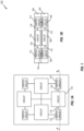
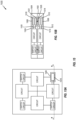
- FIG. 1 is a simplified example of a 3D-IC 100 in accordance with some aspects of the disclosure.
- FIG. 1 includes a plan view as shown in FIG. 1A , and a side sectional view as shown in FIG. 1B taken from the view A-A of FIG. 1A .
- the 3D-IC 100 includes a first die 102 lying within a first geometric plane and a second die 104 lying within a second geometric plane.
- the first and second dies 102 and 104 are parallel to one another and in a stacked arrangement.
- the second die 104 is stacked on top of the first die 102.
- Other die configurations may be employed in other implementations.
- a 3D-IC implemented in accordance with the teachings herein may include more than two dies.
- the dies are not stacked on top of the other.
- the dies are not parallel (i.e., the dies lie in geometric planes that are not parallel with respect to one another).
- Each of the dies includes electrically coupled switch circuits and other circuits (e.g., logic circuits, digital circuits, analog circuits, and so on).
- the first die 102 includes switch circuits 106 and circuits 108, where at least one of the switch circuits 106 is electrically coupled to at least one of the circuits 108 via at least one electrical path 110 (e.g., a signal bus).
- the second die 104 includes switch circuits 112 and circuits 114, where at least one of the switch circuits 112 is electrically coupled to at least one of the circuits 114 via at least one electrical path 116 (e.g., a signal bus).
- interconnections e.g., an electrical path 118 are provided between the switch circuits 106 and 112.
- each switch circuit supports one or more of: programmable signal routing, distribution of a voltage supply, distribution of multiple voltage supplies, or voltage level shifting.
- a switch circuit may be referred to herein as a peripheral switch (e.g., indicating that the switch may be separate from other circuit components of an IC).
- a voltage control circuit (e.g., including a voltage regulator) can be integrated into a switch circuit to provide one or more voltages for an individual die.
- switch circuits on different dies may each be coupled to a power distribution path on the respective die.
- switch circuits on different dies may each include a supply voltage control circuit.
- each of the supply voltage control circuits may generate a plurality of supply voltage levels.
- a level shifter can be included in a switch circuit to shift signal levels between different power supply domains.
- switch circuits on different dies may each be coupled to a power distribution path on the respective die.
- a switch circuit can reroute test signals from one die to another.
- switch circuits on different dies may each be coupled to a test signal path on the respective die.
- this dynamic switching functionality can be used to bypass a failed die by rerouting signals. The switch is thus valuable during the IC (chip) "bring-up" stage since it can be used to isolate the verification target and isolate the root cause of a failure.
- Switch circuits as discussed herein may provide digital and/or analog connectivity.
- Digital switch circuitry may connect, for example and without limitation, one or more of: digital logic circuits, digital memory circuits, or digital power distribution circuits.
- Analog switch circuitry may connect, for example and without limitation, one or more of: analog logic circuits, analog power distribution circuits, analog radio frequency (RF) circuits (e.g., RF transmitter and/or RF receiver circuits), analog phase locked loop (PLL) circuits, or analog circuitry of digital-to-analog converter (DAC) circuits and/or analog-to-digital converter (DAC) circuits.
- RF radio frequency
- PLL phase locked loop
- a conventional 3D-IC is implemented using either a 2.5D interposer architecture or fully stacked 3D architecture.
- a 2.5D interposer architecture multiple dies are placed on top of an interposer and connected together through TSVs and a flip chip configuration. This approach reuses current system-on-chip (SoC) design methodology to shorten the design cycle as well as reduce the design cost.
- SoC system-on-chip
- the interposer is manufactured with mature main stream technology to further offset the cost.
- SiP system-in-package
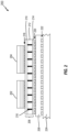
- FIG. 2 is a side sectional view of a simplified example of a conventional 2.5D IC 200.
- the 2.5D IC 200 includes a first die 202 and a second die 204.
- a silicon interposer 206 is placed between a SiP substrate 208 and the dice 202 and 204.
- the silicon interposer 206 includes topside metal layers 210, an interposer substrate 212, and backside metal layers 214.
- the silicon interposer 206 also includes through-silicon vias (TSVs) 216 connecting the metallization layers 210 and 214 on the upper and lower surfaces.
- TSVs through-silicon vias
- Micro-bumps 218 attach the dice 202 and 204 and the interposer 206.
- the interposer 206 is attached to the SiP substrate 208 via flip-chip bumps 220.
- Package bumps 222 attach the SiP substrate 208 to a circuit board 224.
- the tracks on the topside and backside metal layers of the interposer 206 are created using the same process as the track on the silicon chip, which resolves a major problem of two-dimensional (2D) ICs due to the size difference of tracks on substrate and those on dice. This discrepancy in 2D architectures results in performance loss and increased power consumption.
- a fully stacked 3D architecture multiple dies are stacked together and connected through on-die TSVs. This can improve the overall system performance as well as reduce the cost.
- fully stacked 3D-ICs are seen as a desirable alternative to overcome interconnect scaling issues that can be a major bottleneck on 2D ICs.
- Fully stacked 3D-ICs with the advantage of a smaller footprint area, reduce the wire length on each layer.
- TSV technology is implemented for vertical interconnect between dies, which reduces the long cross-chip interconnects that may exist in 2D ICs.
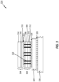
- FIG. 3 is a side sectional view of a simplified example of a conventional fully stacked 3D-IC 300.
- the 3D-IC 300 includes a first die 302 and a second die 304.
- the first die 302 includes backside metal layers 306, a chip substrate 308, a device layer 310, and standard metal layers 312.
- the second die 304 includes a chip substrate 314, a device layer 316, and standard metal layers 318.
- the first die 302 includes TSVs 320 for connecting the metallization layers 306 and 312 on the upper and lower surfaces.
- Micro-bumps 322 attach the dice 302 and 304.
- the first die 302 is attached to a SiP substrate 324 via flip-chip bumps 326.
- Package bumps 328 attach the SiP substrate 324 to a circuit board 330.
- the 3D-IC stacks dices directly and implements the routing in the intermediate dices. Since the thickness of an individual die is very small, ideally one could mount as many dices as needed. In practice, however, there are several challenges involved in manufacturing 3D-ICs, which restricts the application of 3D-ICs.
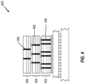
- the typical 3D-IC PDN is implemented as a pyramid shape where additional power rails supply power from the bottom die to the top die.
- FIG. 4 is a side sectional view of such a power distribution network in a conventional 3D-IC 400.
- the 3D-IC 400 includes a first die 402, a second die 404, and a third die 406.
- Each of the dice includes TSVs 408 for connecting, for example, respective metallization layers on upper and lower surfaces.
- the PDN TSVs 408 occupy significant die area and can create a routing congestion problem, particularly, on the lower dies. Moreover, in modern IC design, the current*resistance (IR) drop may be significant even if TSVs are used because the margin working voltage is smaller.
- IR current*resistance
- PDNs have conventionally supplied only a restricted voltage scale because the PDNs use a single power supply from the circuit board. Therefore, the voltage only scales down as the supply passes from one layer to the next (e.g., due to IR drop). Moreover, a higher voltage in the lower layer leads to more severe thermal issues in that layer.
- Another challenge in 3D-IC design relates to thermal management.
- thermal management When multiple dies are stacked together, it is difficult to dissipate the heat, especially for bottom dies. The overall system performance is dramatically degraded at high temperature.
- the use of micro-channels and liquid cooling has been proposed for 3D-IC designs; however, this technology has major drawbacks due to additional hardware requirements and operation difficulty.
- the use of additional TSVs can improve the heat dissipation, however, this may negatively impact the usable area on the die and the amount of stress the die can withstand.
- testing methodology presents a challenge for 3D-IC design. It may be impractical or impossible to fully test the dies before packaging. Thus, traditional Known Good Die (KGD) procedures may be inapplicable. IEEE 1500 has been proposed to resolve this issue using an embedded testing approach; however, this approach is still under development.
- the disclosure relates in some aspects to a 3D-IC hybrid architecture that includes programmable switch routing along with configuration advantages of the 2.5D and fully stacked 3D architectures.
- the architecture of FIG. 5 not only resolves PDN design and thermal management issues, but also provides additional power control and programmable routing capability for 3D-IC design.
- the third layer L3 lies within a third geometric plane.
- the third interposer layer 506 includes wire traces for electrically coupling the dice 532 and 534 of the third die layer D3.
- a portion of the stacked dice 532 and 534 includes at least one peripheral switch for wire routing in another dimension (a vertical dimension in the perspective of FIG. 5 ) to connect the third layer L3 to the other layers.
- Another portion of the stacked dice 532 and 534 includes at least one other circuit (e.g., at least one logic circuit, at least one digital circuit, at least one analog circuit, etc.).
- Each of the first, second and third layers L1, L2, and L3 includes TSVs as represented by the thick vertical lines.
- a TSV 536 is specifically referenced in the third interposer layer 506 and a TSV 538 is specifically referenced in the third die layer D3.
- FIG. 5 also illustrates the bonding and interconnections within and between the first, second and third layers L1, L2, and L3 and other components of the 3D-IC 500.
- Bumps e.g., solder balls
- Bumps 542 attach the dice of the second layer L2 to the second interposer layer 504.
- Bumps 544 attach the dice of the third layer L3 to the third interposer layer 506.
- Bumps 546 attach the stacked dice of the first layer L1.
- Bumps 548 attach the stacked dice of the second layer L2.
- Bumps 550 attach the stacked dice of the third layer L3.
- Bumps 552 attach the dice of the first layer L1 to the second interposer layer 504.
- Bumps 554 attach the dice of the second layer L2 to the third interposer layer 506.
- Bumps 558 attach the first interposer layer 502 to a SiP substrate 556.
- Bumps 562 attach the SiP substrate 556 to a circuit board 560.
- the peripheral switches can be used to reroute signals between layers by dynamically coupling at least one signal path on one layer (e.g., a signal bus, a test signal path, a power distribution path, etc.) to at least one signal path on at least one other layer.
- the 3D-IC 500 can be reprogrammable for different applications.
- the switches are dynamically programmable switches and the signal path on the one layer and in the at least one other layer are test signal paths.
- a PDN can be routed from the bottom substrate through vertical peripheral switches and horizontal interposers to supply power to upper dies.
- this architecture may significantly reduce the PDN area in the bottom active dies and mitigate routing congestion problems.
- each fabricated layer (e.g., die) in a 3D-IC can be identical (the peripheral switches may subsequently be programmed to provide the desired routing).
- a 3D-IC constructed in accordance with the teachings herein may be easier to design and manufacture.
- PDN signals Other types of signals (i.e., not just PDN signals) can be routed through peripheral switches in accordance with the teachings herein.
- critical signals could be routed to different dies through the interposer and peripheral switch.
- a voltage control circuit and regulator can be integrated into a peripheral switch to supply different voltages to the individual die.
- a peripheral switch can include an additional level shifter and a storage unit to transfer the signals among different power domains and even store the data before shut down of the individual die.
- a peripheral switch can be implemented using a low cost, main stream process with large feature geometry. Consequently, the disclosed architecture is highly suitable for voltage regulator implementations and reduced product cost. Moreover, a peripheral switch can be implemented in different 3D-ICs to improve the overall flexibility.
- the disclosed architecture not only increases design feasibility, it can facilitate bypassing a failed die and rerouting the signals to preserve the overall integrity of the IC. This functionality is valuable in the chip bring-up stage since it can be used to isolate the verification target and identify the root cause of a failure.
- peripheral switching as taught herein supports a multiple voltage supply mechanism as well as programmable routing for heterogeneous integration.
- peripheral switching as taught herein can provide predefined dynamic power control and a routing switch center.
- several dies with different functionality can integrated into single package without some of the routing congestion and heat dissipation problems seen in conventional architectures.
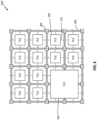
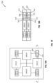
- FIG. 6 is a plan view of a simplified example of a 3D-IC 600 in accordance with some aspects of the disclosure.
- Logic circuits or other types of circuits are represented by the larger tiles (e.g., the largest tile 602 and a medium-sized tile 604).
- Peripheral switches (S) are represented by the smaller tiles (e.g., the peripheral switch 606).
- Routing tracks e.g., a routing track 608) between peripheral switches and/or other circuits are also indicated, as well as input/output (I/O) connections (e.g., an I/O connection 610) between circuits and routing tracks.
- I/O input/output
- a peripheral switch may couple any of the routing tracks from one side (e.g., top, bottom, left or right) of the switch to any other routing track or I/O connection on another side of the switch.
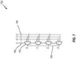
- FIGS. 7 and 8 illustrate two examples of the peripheral switch 606.
- FIG. 7 illustrates an example of a routing switch 700 (e.g., the peripheral switch 606) that includes a series of 4:1 multiplexers (e.g., a multiplexer 702). Each multiplexer couples one of four inputs 704 to a corresponding output 706 according to control signals 708.
- a logic circuit on the die or some other circuit generates the control signals 708 to dynamically control which tracks (e.g., one or more of the routing tracks of FIG. 6 ) the routing switch 700 will couple together at a given point in time.
- tracks e.g., one or more of the routing tracks of FIG. 6
- a routing switch may take other forms in other implementations.
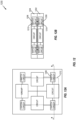
- FIG. 8 illustrates an example of a power switch 800 (e.g., the peripheral switch 606) that includes a series of two input control gates (e.g., a control gate 802).
- the control gates are AND gates.
- the control gates couple power from a given input 804 to a given output 806 according to control signals 808.
- a logic circuit on the die or some other circuit generates the control signals 808 to dynamically control which tracks (e.g., one or more of the routing tracks of FIG. 6 ) the power switch 800 will couple together at a given point in time.
- tracks e.g., one or more of the routing tracks of FIG. 6
- a power switch may take other forms in other implementations.
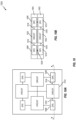
- FIG. 9 is a plan view of a simplified example of peripheral switches in a 3D-IC 900 in accordance with some aspects of the disclosure.
- Logic blocks or other types of circuits are represented by the tiles (e.g., a tile 902).
- Peripheral switches are represented by programmable routing switches (e.g., a routing switch 904) disposed between the tiles.
- This figure also shows signal paths (e.g., a routing track 906) that connect to the logic blocks (or other circuits) and the peripheral switches.
- FIG. 9 also illustrates I/O connections for the tiles including input connections (e.g., an input connection 908) and output connections (e.g., an output connection 910).
- each of the peripheral switches are dynamically switchable.
- a switch circuit may take the form of a crossbar switch and/or a field programmable switch.
- a switch circuit may selectively couple signals to another circuit (e.g., at least one logic circuit, at least one digital circuit, at least one analog circuit, etc.).
- a switch circuit selectively couples test signals to a switch circuit on another die in another layer.
- FIG. 10 is a schematic representation of an example of dynamically programmable switches in a 3D-IC 1000 in accordance with some aspects of the claimed invention.
- FIG. 10 includes a plan view as shown in FIG. 10A , and a side sectional view as shown in FIG. 10B taken from the view A-A of FIG. 10A .
- the 3D-IC includes a first layer (e.g., die) 1002 and a second layer (e.g., die) 1004 stacked on top of the first layer 1002.
- DPSs Dynamically programmable switches
- the second layer 1004 includes DPSs 1006 and 1008, while the first layer 1002 includes DPSs 1012 and 1014. This facilitates connectivity with other components on the respective layer.
- dynamically programmable switches e.g., switches 1006 and 1012 and switches 1008 and 1014.
- switches 1006 and 1012 and switches 1008 and 1014 are stacked in the vertical direction (from this view). This facilitates connectivity between layers, thus enabling signals to be dynamically switched across layers.
- the signal paths e.g., the signal paths 1016 and 1018) between circuits (e.g., the circuits 1020 and 1022) and the dynamically programmable switches (e.g., the switches 1006 and 1012)
- one or more of the circuits of the 3D-IC 1000 may control the dynamically programmable switches.
- one or more of the dynamically programmable switches control another dynamically programmable switch or route corresponding control signals thereto.
- FIG. 11 Signal paths in accordance with the claimed invention are depicted in FIG. 11 where a first die layer 1102 and a second die layer 1104 are coupled to an interposer (interposer layer) 1106.
- a first signal path 1108 of the first die layer 1102 is electrically coupled to a first switch circuit (DPS) 1110.
- DPS first switch circuit
- the first signal path 1108 may be a signal bus, a test signal path, a power distribution path, or some other signal path that is electrically coupled to a first circuit 1112 (e.g., at least one logic circuit, at least one digital circuit, at least one analog circuit, etc.).
- the first signal path is a test signal path.
- a second signal path 1114 of the second die layer 1104 is electrically coupled to a second switch circuit 1116.
- the second signal path 1114 is electrically coupled to a second circuit 1118 (e.g., at least one logic circuit, at least one digital circuit, at least one analog circuit, etc.).
- a third signal path 1120 is routed from the first die layer 1102 to the second die layer 1104 through the interposer 1106, thereby electrically coupling the first switch circuit 1110 and the second switch circuit 1116.
- the first signal path 1108 is dynamically coupled to and uncoupled from the second signal path 1114.
- each of the switch circuits may be located at a periphery of a die.
- heat dissipation on the die may be improved and routing congestion on the die may be mitigated as compared to conventional architectures.
- improved heat transfer may be achieved from the center to the edge of the IC package (e.g., through an RDL and TSVs).
- this scheme is much simpler than micro-channel solutions for thermal management.
- FIG. 12 is a schematic representation of an example of switches located at a periphery of a 3D-IC 1200 in accordance with some aspects of the disclosure.
- FIG. 12 includes a plan view as shown in FIG. 12A , and a side sectional view as shown in FIG. 12B taken from the view A-A of FIG. 12A .
- the 3D-IC 1200 includes a first layer (e.g., die) 1202 and a second layer (e.g., die) 1204. As indicated, a first switch circuit 1206 is located at a first periphery 1210 of the first layer 1202, and a second switch circuit 1208 is located at a second periphery 1212 of the second layer 1204.
- a first switch circuit 1206 is located at a first periphery 1210 of the first layer 1202
- a second switch circuit 1208 is located at a second periphery 1212 of the second layer 1204.
- switch circuits may be used in a power distribution network of a 3D-IC to distribute power to other circuits (e.g., at least one logic circuit, at least one digital circuit, at least one analog circuit, etc.).
- FIG. 13 is a schematic representation of an example of power distribution in a 3D-IC 1300 in accordance with some aspects of the disclosure.
- FIG. 13 includes a plan view as shown in FIG. 13A , and a side sectional view as shown in FIG. 13B taken from the view A-A of FIG. 13A .
- the 3D-IC 1300 includes a first layer (e.g., die) 1302 and a second layer (e.g., die) 1304. As indicated, a first power distribution path 1306 (e.g., for providing power to a first circuit 1308) of the second layer 1304 is electrically coupled to a first switch circuit 1310. Similarly, a second power distribution path 1312 (e.g., for providing power to a second circuit 1314) of the first layer 1302 is electrically coupled to a second switch circuit 1316. In addition, a third power distribution path 1318 electrically couples the first switch circuit 1310 and the second switch circuit 1316. Thus, power may be dynamically switched between layers as needed.
- a first power distribution path 1306 e.g., for providing power to a first circuit 1308
- a second power distribution path 1312 e.g., for providing power to a second circuit 1314
- a third power distribution path 1318 electrically couples the first switch circuit 1310 and the second switch circuit 1316.
- one or more of the switch circuits may each include a power control circuit for supplying power to a corresponding layer (e.g., die layer).
- FIG. 14 is a schematic representation of an example of power control circuits in a 3D-IC 1400 in accordance with some aspects of the disclosure.
- FIG. 14 includes a plan view as shown in FIG. 14A , and a side sectional view as shown in FIG. 14B taken from the view A-A of FIG. 14A .
- the 3D-IC 1400 includes a first layer (e.g., die) 1402 and a second layer (e.g., die) 1404.
- a first switch circuit 1406 on the first layer 1402 includes a first supply voltage control circuit (SVCC) 1410
- SVCC first supply voltage control circuit
- a second switch circuit 1408 on the second layer 1404 includes a second supply voltage control circuit 1412.
- the first SVCC 1410 may control power supplied to a first circuit 1414 (e.g., at least one logic circuit, at least one digital circuit, at least one analog circuit, etc.) via a first supply path 1416 on the first layer 1402.
- the second SVCC 1412 may control power supplied to a second circuit 1418 (e.g., at least one logic circuit, at least one digital circuit, at least one analog circuit, etc.) via a second supply path 1420 on the second layer 1404. Accordingly, independent power control can be provided on a layer-by-layer basis through the use of peripheral switches as taught herein. Moreover, in some aspects, the first SVCC 1410 and the second SVCC 1412 may cooperate via signaling 1422 to provide power to the different layers.
- a second circuit 1418 e.g., at least one logic circuit, at least one digital circuit, at least one analog circuit, etc.
- the first SVCC 1410 and the second SVCC 1412 may cooperate via signaling 1422 to provide power to the different layers.
- more than one power supply voltage level may be used on a given die.
- one or more of the supply voltage control circuits of FIG. 14 may each generate a plurality of supply voltage levels used by different voltage domains on a respective die.
- FIG. 15 is a schematic representation of an example of multi-level supply voltage circuits in a 3D-IC 1500 in accordance with some aspects of the disclosure.
- FIG. 15 includes a plan view as shown in FIG. 15A , and a side sectional view as shown in FIG. 15B taken from the view A-A of FIG. 15A .
- the 3D-IC 1500 includes a first layer (e.g., die) 1502 and a second layer (e.g., die) 1504.
- a first switch circuit 1506 on the first layer 1502 includes a first voltage supply circuit 1510 coupled to a first supply path 1512 of the first layer 1502 and a second voltage supply circuit 1514 coupled to a second supply path 1516 of the first layer 1502.
- a second switch circuit 1508 on the second layer 1504 includes a first voltage supply circuit 1518 coupled to a first supply path 1520 of the second layer 1504 and a second voltage supply circuit 1522 coupled to a second supply path 1524 of the second layer 1504.
- different power levels can be independently provided on a layer-by-layer basis through the use of peripheral switches as taught herein.
- different dies manufactured using different processes may employ different power levels (e.g., 3.5 V versus 1.8 V).
- a single power supply voltage e.g., a main supply signal 1526
- the voltage supply circuit(s) on each peripheral switch provides the appropriate voltage level(s) for the die(s) on the corresponding level.
- one or more of the switch circuits may each include a voltage shifter circuit that is used to shift the level of a signal on a respective die.
- the level of a signal may need to be shifted to accommodate different voltage domains (e.g., on different dies) that use different supply voltage levels.
- FIG. 16 is a schematic representation of an example of signal level shifter circuits in a 3D-IC 1600 in accordance with some aspects of the disclosure.
- FIG. 16 includes a plan view as shown in FIG. 16A , and a side sectional view as shown in FIG. 16B taken from the view A-A of FIG. 16A .
- the 3D-IC 1600 includes a first layer (e.g., die) 1602 and a second layer (e.g., die) 1604.
- a first switch circuit 1606 on the first layer 1602 includes a first voltage level shifter (VLS) 1610 coupled to a first signal path 1612 and a second signal path 1614 of the first layer 1602.
- VLS voltage level shifter
- the first VLS 1610 may shift the signaling level of a signal received on the first signal path 1612 (e.g., from one die) to a different signaling level and output the resulting signal on the second signal path 1614 (e.g., to a different die).
- a second switch circuit 1608 on the second layer 1604 includes a second VLS 1616 coupled to a third signal path 1618 and a fourth signal path 1620 of the second layer 1604. Accordingly, the second VLS 1616 may shift the signaling level of a signal received on the third signal path 1618 to a different signaling level and output the resulting signal on the fourth signal path 1620.
- a memory device e.g., a register file
- a peripheral switch can be included in a peripheral switch to store data.
- data from a die may be stored in such a memory device prior to shutting down the individual die (e.g., due to a fault condition).
- FIG. 17 is a schematic representation of an example of memory circuits in a 3D-IC 1700 in accordance with some aspects of the disclosure.
- FIG. 17 includes a plan view as shown in FIG. 17A , and a side sectional view as shown in FIG. 17B taken from the view A-A of FIG. 17A .
- the 3D-IC 1700 includes a first layer (e.g., die) 1702 and a second layer (e.g., die) 1704.
- a first switch circuit 1706 on the first layer 1702 includes a first memory device (MD) 1710 that is coupled to a first signal path 1712 of the first layer 1702.
- a second switch circuit 1708 on the second layer 1704 includes a second memory device 1714 that is coupled to a second signal path 1716 of the second layer 1704.
- data from a first circuit 1718 (e.g., at least one logic circuit, at least one digital circuit, at least one analog circuit, etc.) on the first layer 1702 and/or a second circuit 1720 (e.g., at least one logic circuit, at least one digital circuit, at least one analog circuit, etc.) on the second layer 1704 may be stored in the first MD 1710 and/or the second MD 1714.
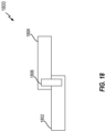
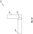
- dies may be oriented with respect to each other in different ways in different implementations.
- FIGs. 18 - 20 illustrate three non-limiting examples of potential orientations.
- FIG. 18 is a side view of a simplified example of offset dies 1800 in accordance with some aspects of the disclosure.
- a first die 1802 is offset (horizontally in this view) from a second die 1804.
- at least one peripheral switch 1806 is included in and/or coupled to each of the first and second dies 1802 and 1804.
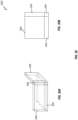
- FIG. 19 is a side view of a simplified example of dies in different geometric planes 1900 in accordance with some aspects of the disclosure.
- a first die 1902 is at a right angle to a second die 1904.
- at least one peripheral switch 1906 is included in and/or coupled to each of the first and second dies 1902 and 1904.
- FIG. 20 is a simplified example of dies in different geometric planes 2000 in accordance with some aspects of the disclosure.
- FIG. 20 includes a perspective view as shown in FIG. 20A , and a plan view as shown in FIG. 20B .
- a first die 2002, a second die 2004, and a third die 2006 are all at right angles with respect to one another.
- at least one peripheral switch 2008 is included in and/or coupled to each of the first die 2002, the second die 2004, and the third die 2006.
- dies need not be disposed at right angles as shown in FIGs. 19 and 20 . Rather, it may be advantageous to route dies at other angles in some implementations.
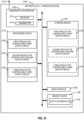
- FIG. 21 is an illustration of an apparatus 2100 that may be implemented as a 3D-IC according to one or more aspects of the disclosure.
- the apparatus 2100 includes a communication interface (e.g., at least one transceiver) 2102, a storage medium 2104, a user interface 2106, a memory device 2108, and a processing circuit 2110.
- the signaling bus may include any number of interconnecting buses and bridges depending on the specific application of the processing circuit 2110 and the overall design constraints.
- the signaling bus links together various circuits such that each of the communication interface 2102, the storage medium 2104, the user interface 2106, and the memory device 2108 are coupled to and/or in electrical communication with the processing circuit 2110.
- the signaling bus may also link various other circuits (not shown) such as timing sources, peripherals, voltage regulators, and power management circuits, which are well known in the art, and therefore, will not be described any further.
- the communication interface 2102 may be adapted to facilitate wireless communication of the apparatus 2100.
- the communication interface 2102 may include circuitry and/or programming adapted to facilitate the communication of information bi-directionally with respect to one or more communication devices in a network.
- the communication interface 2102 may be coupled to one or more antennas 2112 for wireless communication within a wireless communication system.
- the communication interface 2102 can be configured with one or more standalone receivers and/or transmitters, as well as one or more transceivers.
- the communication interface 2102 includes a transmitter 2114 and a receiver 2116.
- the memory device 2108 may represent one or more memory devices. As indicated, the memory device 2108 may maintain switch information 2118 along with other information used by the apparatus 2100. In some implementations, the memory device 2108 and the storage medium 2104 are implemented as a common memory component. The memory device 2108 may also be used for storing data that is manipulated by the processing circuit 2110 or some other component of the apparatus 2100.
- the storage medium 2104 may represent one or more computer-readable, machine-readable, and/or processor-readable devices for storing programming, such as processor executable code or instructions (e.g., software, firmware), electronic data, databases, or other digital information.
- the storage medium 2104 may also be used for storing data that is manipulated by the processing circuit 2110 when executing programming.
- the storage medium 2104 may be any available media that can be accessed by a general purpose or special purpose processor, including portable or fixed storage devices, optical storage devices, and various other mediums capable of storing, containing or carrying programming.
- the storage medium 2104 may include a magnetic storage device (e.g., hard disk, floppy disk, magnetic strip), an optical disk (e.g., a compact disc (CD) or a digital versatile disc (DVD)), a smart card, a flash memory device (e.g., a card, a stick, or a key drive), a random access memory (RAM), a read only memory (ROM), a programmable ROM (PROM), an erasable PROM (EPROM), an electrically erasable PROM (EEPROM), a register, a removable disk, and any other suitable medium for storing software and/or instructions that may be accessed and read by a computer.
- a magnetic storage device e.g., hard disk, floppy disk, magnetic strip
- an optical disk e.g., a compact disc (CD) or a digital versatile disc (DVD)
- a smart card e.g., a flash memory device (e.g., a card, a stick, or
- the storage medium 2104 may be embodied in an article of manufacture (e.g., a computer program product).
- a computer program product may include a computer-readable medium in packaging materials.
- the storage medium 2104 may be a non-transitory (e.g., tangible) storage medium.
- the storage medium 2104 may be coupled to the processing circuit 2110 such that the processing circuit 2110 can read information from, and write information to, the storage medium 2104. That is, the storage medium 2104 can be coupled to the processing circuit 2110 so that the storage medium 2104 is at least accessible by the processing circuit 2110, including examples where at least one storage medium is integral to the processing circuit 2110 and/or examples where at least one storage medium is separate from the processing circuit 2110 (e.g., resident in the apparatus 2100, external to the apparatus 2100, distributed across multiple entities, etc.).
- the storage medium 2104 may include operations configured for regulating operations at one or more hardware blocks of the processing circuit 2110, as well as to utilize the communication interface 2102 for wireless communication utilizing their respective communication protocols.
- the processing circuit 2110 is generally adapted for processing, including the execution of such programming stored on the storage medium 2104.
- programming shall be construed broadly to include without limitation instructions, instruction sets, data, code, code segments, program code, programs, subprograms, software modules, applications, software applications, software packages, routines, subroutines, objects, executables, threads of execution, procedures, functions, etc., whether referred to as software, firmware, middleware, microcode, hardware description language, or otherwise.
- the processing circuit 2110 is arranged to obtain, process and/or send data, control data access and storage, issue commands, and control other desired operations.
- the processing circuit 2110 may include circuitry configured to implement desired programming provided by appropriate media in at least one example.
- the processing circuit 2110 may be implemented as one or more processors, one or more controllers, and/or other structure configured to execute executable programming.
- Examples of the processing circuit 2110 may include a general purpose processor, a digital signal processor (DSP), an application specific integrated circuit (ASIC), a field programmable gate array (FPGA) or other programmable logic component, discrete gate or transistor logic, discrete hardware components, or any combination thereof designed to perform the functions described herein.
- DSP digital signal processor
- ASIC application specific integrated circuit
- FPGA field programmable gate array
- a general purpose processor may include a microprocessor, as well as any conventional processor, controller, microcontroller, or state machine.
- the processing circuit 2110 may also be implemented as a combination of computing components, such as a combination of a DSP and a microprocessor, a number of microprocessors, one or more microprocessors in conjunction with a DSP core, an ASIC and a microprocessor, or any other number of varying configurations. These examples of the processing circuit 2110 are for illustration and other suitable configurations within the scope of the disclosure are also contemplated.
- the processing circuit 2110 may be adapted to perform any or all of the features, processes, functions, operations and/or routines for any or all of the apparatuses described herein.
- the term "adapted" in relation to the processing circuit 2110 may refer to the processing circuit 2110 being one or more of configured, employed, implemented, and/or programmed to perform a particular process, function, operation and/or routine according to various features described herein.
- the processing circuit 2110 may include one or more of a first module for controlling a first switch circuit 2120, a second module for controlling a second switch circuit 2122, and a third module for controlling a third switch circuit 2124.
- the first module for controlling a first switch circuit 2120 may include circuitry and/or programming (e.g., a first module for controlling a first switch circuit 2126 stored on the storage medium 2104) adapted to perform several functions relating to, for example controlling a switch circuit to couple electrical paths on one die to electrical paths on another die. In some aspects, this coupling is achieved via another switch circuit on the other die.
- the first module for controlling a first switch circuit 2120 obtains received information (e.g., from the memory device 2108, the receiver 2116, or some other component). For example, the first module for controlling a first switch circuit 2120 may receive an indication that affects how the switch circuit is to be controlled.
- the first module for controlling a first switch circuit 2120 identifies a memory location in the memory device 2108 that stores the indication and invokes a read of that location. In some implementations, the first module for controlling a first switch circuit 2120 processes the received indication to determine how to control the switch circuit. The first module for controlling a first switch circuit 2120 then generates, based on the received information, a control signal that controls the switch circuit.
- the second module for controlling a second switch circuit 2122 may include circuitry and/or programming (e.g., a second module for controlling a second switch circuit 2128 stored on the storage medium 2104) adapted to perform several functions relating to, for example controlling a switch circuit to couple electrical paths on one die to electrical paths on another die. In some aspects, this coupling is achieved via another switch circuit on the other die.
- the second module for controlling a second switch circuit 2122 obtains received information (e.g., from the memory device 2108, the receiver 2116, or some other component). For example, the second module for controlling a second switch circuit 2122 may receive an indication that affects how the switch circuit is to be controlled.
- the second module for controlling a second switch circuit 2122 identifies a memory location in the memory device 2108 that stores the indication and invokes a read of that location. In some implementations, the second module for controlling a second switch circuit 2122 processes the received indication to determine how to control the switch circuit. The second module for controlling a second switch circuit 2122 then generates, based on the received information, a control signal that controls the switch circuit.
- the third module for controlling a third switch circuit 2124 may include circuitry and/or programming (e.g., a third module for controlling a third switch circuit 2130 stored on the storage medium 2104) adapted to perform several functions relating to, for example controlling a switch circuit to couple electrical paths on one die to electrical paths on another die. In some aspects, this coupling is achieved via another switch circuit on the other die.
- the third module for controlling a third switch circuit 2124 obtains received information (e.g., from the memory device 2108, the receiver 2116, or some other component). For example, the third module for controlling a third switch circuit 2124 may receive an indication that affects how the switch circuit is to be controlled.
- the third module for controlling a third switch circuit 2124 identifies a memory location in the memory device 2108 that stores the indication and invokes a read of that location. In some implementations, the third module for controlling a third switch circuit 2124 processes the received indication to determine how to control the switch circuit. The third module for controlling a third switch circuit 2124 then generates, based on the received information, a control signal that controls the switch circuit.
- the storage medium 2104 may include one or more of the first module for controlling a first switch circuit 2126, the second module for controlling a second switch circuit 2128, or the third module for controlling a third switch circuit 2130.
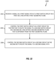
- FIG. 22 illustrates a switching process 2200 in accordance with some aspects of the disclosure.
- the process 2200 may take place within a 3D-IC (e.g., one or more of the 3D-IC of any of FIGs. 1 , 5 , 6 , or 9 - 21 ), at least partially within a processing circuit (e.g., the processing circuit 2110 of FIG. 21 ), which may be located in an electronic device, a transceiver, or some other suitable apparatus.
- a processing circuit e.g., the processing circuit 2110 of FIG. 21
- the process 2200 may be implemented by any suitable apparatus capable of supporting switching operations.
- a signal is received via a first signal path at a first switch circuit.
- the first switch circuit is on a first die that lies within a first geometric plane.
- the signal may take different forms in different implementations.
- the signal may be a test signal (e.g., that is selectively routed between first and second dies).
- the signal may be a power supply voltage signal (e.g., a +3.5 V supply voltage, a -3.5 V supply voltage, etc.).
- the first switch circuit is controlled via a first circuit to route the signal to a second switch circuit.
- the first circuit is on the first die.
- the second switch circuit is on a second die that lies within a second geometric plane. The second geometric plane is different from the first geometric plane.
- the second switch circuit is controlled via a second circuit to route the signal to a second signal path.
- the second circuit is on the second die.
- the first and second circuits include logic circuits. In some aspects, the first and second switch circuits include analog switch circuitry.
- the first and second die may be oriented relative to one another in various ways.
- the second die is stacked on top of the first die.
- the first and second geometric planes are parallel, while in other cases they might not be.
- the signal is routed to at least one other die.
- the process 2200 also may include controlling the second switch circuit via the second logic circuit to route the signal to a third switch circuit, where the third circuit is on a third die lying within a third geometric plane that is different from the first and second geometric planes.
- the process 2200 may then include controlling the third switch circuit via a third logic circuit to route the signal to a third signal path, where the third logic circuit is on the third die.
- FIG. 23 illustrates a process 2300 for handling a fault condition in accordance with some aspects of the disclosure.
- the process 2300 may take place within a 3D-IC (e.g., one or more of the 3D-IC of any of FIGs. 1 , 5 , 6 , or 9 - 21 ), at least partially within a processing circuit (e.g., the processing circuit 2110 of FIG. 21 ), which may be located in an electronic device, a transceiver, or some other suitable apparatus.
- a processing circuit e.g., the processing circuit 2110 of FIG. 21
- the process 2300 may be implemented by any suitable apparatus capable of supporting fault operations.
- a fault condition is identified on the first die. For example, a diagnostic test performed on a component of the first die may have returned a failure indication.
- routing of the signal to the second signal path may be triggered as a result of the identification of the fault condition at block 2302.
- the first die is disabled as a result of the identification of the fault condition at block 2303.
- the first switch circuit may be controlled via a first circuit (e.g., a logic circuit) to route the signal to a memory device on the second die.
- a first circuit e.g., a logic circuit
Landscapes
- Engineering & Computer Science (AREA)
- General Engineering & Computer Science (AREA)
- Physics & Mathematics (AREA)
- General Physics & Mathematics (AREA)
- Semiconductor Integrated Circuits (AREA)
- Design And Manufacture Of Integrated Circuits (AREA)
Claims (8)
- Eine integrierte Schaltung, die aufweist:einen ersten Die bzw. Chip (1002), der in einer ersten geometrischen Ebene liegt und eine erste Schaltung (1022) und einen ersten Schalterstromkreis (1012, 1014) und einen ersten Signalpfad (1018) zwischen der ersten Schaltung und dem ersten Schalterstromkreis aufweist, wobei der erste Schalterstromkreis und der erste Signalpfad elektrisch mit der ersten Schaltung gekoppelt sind;einen zweiten Die (1004), der in einer zweiten geometrischen Ebene liegt, die sich von der ersten geometrischen Ebene unterscheidet, wobei der zweite Die eine zweite Schaltung (1020) und einen zweiten Schalterstromkreis (1006, 1008) und einen zweiten Signalpfad (1016) zwischen der zweiten Schaltung und dem zweiten Schalterstromkreis aufweist, wobei der zweite Schalterstromkreis elektrisch mit der zweiten Schaltung und dem zweiten Signalpfad gekoppelt ist;und einen dritten Signalpfad (1024), der von dem ersten Schalterstromkreis (1014) zu dem zweiten Schalterstromkreis (1008) führt und den ersten Schalterstromkreis mit dem zweiten Schalterstromkreis elektrisch koppelt;wobei sowohl der erste Schalterstromkreis (1014) als auch der zweite Schalterstromkreis (1008) einen dynamisch programmierbaren Schalter aufweisen, dadurch gekennzeichnet, dass die dynamisch programmierbaren Schalter konfiguriert sind zum dynamischen Koppeln des ersten Signalpfads mit dem zweiten Signalpfad und Entkoppeln des ersten Signalpfads von dem zweiten Signalpfad, wobei der der erste Signalpfad ein Testsignalpfad ist und der zweite Signalpfad ein Testsignalpfad ist.
- Die integrierte Schaltung gemäß Anspruch 1, wobei der zweite Die (1004) auf dem ersten Die gestapelt ist.
- Die integrierte Schaltung gemäß Anspruch 1, wobei:der erste Schalterstromkreis (1012, 1014) eine erste Versorgungsspannungssteuerschaltung aufweist; undder zweite Schalterstromkreis (1006, 1008) eine zweite Versorgungsspannungssteuerschaltung aufweist.
- Die integrierte Schaltung gemäß Anspruch 1, wobei:der erste Schalterstromkreis (1012, 1014) sich an einem ersten Rand des ersten Dies befindet; undder zweite Schalterstromkreis (1006, 1008) sich an einem zweiten Rand des zweiten Dies befindet.
- Die integrierte Schaltung gemäß Anspruch 1, die weiter aufweist:
einen dritten Die (2006), der in einer dritten geometrischen Ebene liegt, die sich von der ersten und zweiten geometrischen Ebene unterscheidet, wobei der dritte Die eine dritte Schaltung und einen dritten Schalterstromkreis aufweist, wobei der dritte Schalterstromkreis elektrisch mit der dritten Schaltung und mit dem ersten und dem zweiten Schalterstromkreis gekoppelt ist. - Eine integrierte Schaltung, die aufweist:eine erste Interposer-Schicht (502), die in einer ersten geometrischen Ebene liegt;eine erste Die-Schicht (D1, 1102), die auf der ersten Interposer-Schicht gestapelt ist und einen ersten Die, einen zweiten Die und einen ersten Signalpfad zwischen einer ersten Schaltung und einem ersten Schalterstromkreis aufweist, wobei der erste Die die erste Schaltung aufweist, der zweite Die den ersten Schalterstromkreis aufweist, wobei der erste Schalterstromkreis elektrisch mit der ersten Schaltung und dem ersten Signalpfad gekoppelt ist;eine zweite Interposer-Schicht (504, 1106), die in einer zweiten geometrischen Ebene liegt, die sich von der ersten geometrischen Ebene unterscheidet;eine zweite Die-Schicht (D2, 1104), die auf der zweiten Interposer-Schicht gestapelt ist und einen dritten Die und einen vierten Die und einen zweiten Signalpfad zwischen einer zweiten Schaltung und einem zweiten Schalterstromkreis aufweist, wobei der dritte Die die zweite Schaltung aufweist, der vierte Die den zweiten Schalterstromkreis aufweist, wobei der zweite Schalterstromkreis elektrisch mit der zweiten Schaltung und dem zweiten Signalpfad gekoppelt ist; undeinen dritten Signalpfad (1120), der von der ersten Die-Schicht durch die zweite Interposer-Schicht zu der zweiten Die-Schicht führt und elektrisch mit dem ersten Schalterstromkreis und dem zweiten Schalterstromkreis gekoppelt ist;wobei sowohl der erste Schalterstromkreis als auch der zweite Schalterstromkreis jeweils einen dynamisch programmierbaren Schalter aufweisen, dadurch gekennzeichnet, dass die dynamisch programmierbaren Schalter konfiguriert sind zum dynamischen Koppeln des ersten Signalpfads mit dem zweiten Signalpfad und Entkoppeln des ersten Signalpfads von dem zweiten Signalpfad, wobei der der erste Signalpfad ein Testsignalpfad ist und der zweite Signalpfad ein Testsignalpfad ist.
- Die integrierte Schaltung gemäß Anspruch 6, wobei die zweite Interposer-Schicht (504) auf der ersten Die-Schicht (D1) gestapelt ist.
- Die integrierte Schaltung gemäß Anspruch 6, die weiter aufweist:eine dritte Interposer-Schicht (506), die in einer dritten geometrischen Ebene liegt, die sich von der ersten und zweiten geometrischen Ebene unterscheidet; undeine dritte Die-Schicht (D3), die auf der dritten Interposer-Schicht gestapelt ist und einen fünften Die und einen sechsten Die aufweist, wobei der fünfte Die eine dritte Schaltung aufweist, der sechste Die einen dritten Schalterstromkreis aufweist, wobei der dritte Schalterstromkreis elektrisch mit der dritten Schaltung und dem ersten und dem zweiten Schalterstromkreis gekoppelt ist.
Applications Claiming Priority (2)
| Application Number | Priority Date | Filing Date | Title |
|---|---|---|---|
| US14/598,052 US9666562B2 (en) | 2015-01-15 | 2015-01-15 | 3D integrated circuit |
| PCT/US2015/065103 WO2016114878A1 (en) | 2015-01-15 | 2015-12-10 | 3d integrated circuit |
Publications (3)
| Publication Number | Publication Date |
|---|---|
| EP3245673A1 EP3245673A1 (de) | 2017-11-22 |
| EP3245673B1 true EP3245673B1 (de) | 2025-06-25 |
| EP3245673C0 EP3245673C0 (de) | 2025-06-25 |
Family
ID=55069125
Family Applications (1)
| Application Number | Title | Priority Date | Filing Date |
|---|---|---|---|
| EP15819969.5A Active EP3245673B1 (de) | 2015-01-15 | 2015-12-10 | 3d-integrierte schaltung |
Country Status (6)
| Country | Link |
|---|---|
| US (1) | US9666562B2 (de) |
| EP (1) | EP3245673B1 (de) |
| JP (1) | JP6324633B2 (de) |
| CN (1) | CN107112313B (de) |
| TW (1) | TWI611191B (de) |
| WO (1) | WO2016114878A1 (de) |
Families Citing this family (28)
| Publication number | Priority date | Publication date | Assignee | Title |
|---|---|---|---|---|
| US10539617B2 (en) | 2016-06-02 | 2020-01-21 | Taiwan Semiconductor Manufacturing Co., Ltd. | Scan architecture for interconnect testing in 3D integrated circuits |
| US9871020B1 (en) * | 2016-07-14 | 2018-01-16 | Globalfoundries Inc. | Through silicon via sharing in a 3D integrated circuit |
| KR102615775B1 (ko) * | 2017-01-31 | 2023-12-20 | 에스케이하이닉스 주식회사 | 반도체 장치 |
| US11398453B2 (en) * | 2018-01-09 | 2022-07-26 | Samsung Electronics Co., Ltd. | HBM silicon photonic TSV architecture for lookup computing AI accelerator |
| US10664643B2 (en) * | 2018-02-09 | 2020-05-26 | University Of Louisiana At Lafayette | Method for the non-copyable manufacture of integrated circuits |
| US11041211B2 (en) | 2018-02-22 | 2021-06-22 | Xilinx, Inc. | Power distribution for active-on-active die stack with reduced resistance |
| FR3082656B1 (fr) | 2018-06-18 | 2022-02-04 | Commissariat Energie Atomique | Circuit integre comprenant des macros et son procede de fabrication |
| US10826492B2 (en) * | 2018-08-31 | 2020-11-03 | Xilinx, Inc. | Power gating in stacked die structures |
| US12019527B2 (en) | 2018-12-21 | 2024-06-25 | Graphcore Limited | Processor repair |
| US12469783B2 (en) * | 2019-04-26 | 2025-11-11 | Graphcore Limited | Communication between stacked die |
| US11437376B2 (en) * | 2019-05-31 | 2022-09-06 | Tokyo Electron Limited | Compact 3D stacked-CFET architecture for complex logic cells |
| US11217563B2 (en) * | 2019-10-24 | 2022-01-04 | Apple Inc. | Fully interconnected heterogeneous multi-layer reconstructed silicon device |
| US11610921B2 (en) * | 2019-12-12 | 2023-03-21 | Au Optronics Corporation | Chip having a flexible substrate |
| TWI747288B (zh) * | 2019-12-12 | 2021-11-21 | 友達光電股份有限公司 | 晶片 |
| US12255148B2 (en) * | 2020-04-30 | 2025-03-18 | Taiwan Semiconductor Manufacturing Company, Ltd. | Power distribution structure and method |
| DE102021104688A1 (de) * | 2020-04-30 | 2021-11-04 | Taiwan Semiconductor Manufacturing Co., Ltd. | Stromverteilungsstruktur und verfahren |
| KR102792976B1 (ko) * | 2020-08-31 | 2025-04-11 | 에스케이하이닉스 주식회사 | 적층 반도체 칩을 포함하는 반도체 패키지 |
| JP2022047010A (ja) * | 2020-09-11 | 2022-03-24 | キオクシア株式会社 | 磁気記憶装置 |
| KR102924473B1 (ko) | 2020-10-28 | 2026-02-05 | 삼성전자 주식회사 | 집적 회로 반도체 소자 |
| WO2022145320A1 (ja) * | 2020-12-28 | 2022-07-07 | 株式会社村田製作所 | 高周波回路 |
| US11978723B2 (en) * | 2021-03-31 | 2024-05-07 | Taiwan Semiconductor Manufacturing Company, Ltd. | Vertical interconnect structures in three-dimensional integrated circuits |
| US11942453B2 (en) | 2021-08-05 | 2024-03-26 | Kambix Innovations, Llc | Thermal management of three-dimensional integrated circuits |
| US11710723B2 (en) | 2021-08-05 | 2023-07-25 | Kambix Innovations, Llc | Thermal management of three-dimensional integrated circuits |
| US11816357B2 (en) * | 2021-08-12 | 2023-11-14 | Micron Technology, Inc. | Voltage regulation distribution for stacked memory |
| WO2023023079A1 (en) * | 2021-08-19 | 2023-02-23 | Tesla, Inc. | Bypass routing |
| US20230223402A1 (en) * | 2022-01-12 | 2023-07-13 | Kneron Inc. | Three-dimensional Integrated Circuit |
| US20230258886A1 (en) * | 2022-02-16 | 2023-08-17 | Taiwan Semiconductor Manufacturing Company, Ltd. | Semiconductor package structure with multiple waveguides |
| US12355006B2 (en) * | 2022-02-16 | 2025-07-08 | Taiwan Semiconductor Manufacturing Company, Ltd. | Semiconductor packages and methods of manufacturing thereof |
Citations (2)
| Publication number | Priority date | Publication date | Assignee | Title |
|---|---|---|---|---|
| US20090080279A1 (en) * | 2007-09-25 | 2009-03-26 | Jung Pill Kim | Structure to share internally generated voltages between chips in mcp |
| US20100091537A1 (en) * | 2006-12-14 | 2010-04-15 | Best Scott C | Multi-die memory device |
Family Cites Families (18)
| Publication number | Priority date | Publication date | Assignee | Title |
|---|---|---|---|---|
| JP2810944B2 (ja) * | 1989-03-20 | 1998-10-15 | 株式会社日立製作所 | 半導体記憶装置 |
| JP4291596B2 (ja) * | 2003-02-26 | 2009-07-08 | 株式会社ルネサステクノロジ | 半導体集積回路の試験装置およびそれを用いた半導体集積回路の製造方法 |
| JP4371769B2 (ja) * | 2003-10-27 | 2009-11-25 | 株式会社ルネサステクノロジ | 半導体回路デバイス及びデータ処理システム |
| JP2006286048A (ja) * | 2005-03-31 | 2006-10-19 | Toshiba Corp | 半導体記憶装置 |
| US7692946B2 (en) * | 2007-06-29 | 2010-04-06 | Intel Corporation | Memory array on more than one die |
| US8679861B2 (en) * | 2007-11-29 | 2014-03-25 | International Business Machines Corporation | Semiconductor chip repair by stacking of a base semiconductor chip and a repair semiconductor chip |
| JP5325495B2 (ja) * | 2008-08-12 | 2013-10-23 | 学校法人慶應義塾 | 半導体装置及びその製造方法 |
| US8604603B2 (en) | 2009-02-20 | 2013-12-10 | The Hong Kong University Of Science And Technology | Apparatus having thermal-enhanced and cost-effective 3D IC integration structure with through silicon via interposers |
| US8547769B2 (en) | 2011-03-31 | 2013-10-01 | Intel Corporation | Energy efficient power distribution for 3D integrated circuit stack |
| US20120327714A1 (en) * | 2011-06-23 | 2012-12-27 | Macronix International Co., Ltd. | Memory Architecture of 3D Array With Diode in Memory String |
| US8624626B2 (en) | 2011-11-14 | 2014-01-07 | Taiwan Semiconductor Manufacturing Co., Ltd. | 3D IC structure and method |
| US9229466B2 (en) * | 2011-12-31 | 2016-01-05 | Intel Corporation | Fully integrated voltage regulators for multi-stack integrated circuit architectures |
| TWI489464B (zh) * | 2012-01-17 | 2015-06-21 | Macronix Int Co Ltd | 具有讀取位元線屏蔽之三維記憶體陣列 |
| US8778734B2 (en) | 2012-03-28 | 2014-07-15 | Advanced Micro Devices, Inc. | Tree based adaptive die enumeration |
| US8866281B2 (en) | 2012-07-19 | 2014-10-21 | Nanya Technology Corporation | Three-dimensional integrated circuits and fabrication thereof |
| US8872322B2 (en) | 2012-10-22 | 2014-10-28 | International Business Machines Corporation | Stacked chip module with integrated circuit chips having integratable built-in self-maintenance blocks |
| US9170948B2 (en) | 2012-12-23 | 2015-10-27 | Advanced Micro Devices, Inc. | Cache coherency using die-stacked memory device with logic die |
| US9065722B2 (en) | 2012-12-23 | 2015-06-23 | Advanced Micro Devices, Inc. | Die-stacked device with partitioned multi-hop network |
-
2015
- 2015-01-15 US US14/598,052 patent/US9666562B2/en active Active
- 2015-12-10 JP JP2017536925A patent/JP6324633B2/ja not_active Expired - Fee Related
- 2015-12-10 EP EP15819969.5A patent/EP3245673B1/de active Active
- 2015-12-10 CN CN201580073361.1A patent/CN107112313B/zh active Active
- 2015-12-10 WO PCT/US2015/065103 patent/WO2016114878A1/en not_active Ceased
- 2015-12-11 TW TW104141818A patent/TWI611191B/zh not_active IP Right Cessation
Patent Citations (2)
| Publication number | Priority date | Publication date | Assignee | Title |
|---|---|---|---|---|
| US20100091537A1 (en) * | 2006-12-14 | 2010-04-15 | Best Scott C | Multi-die memory device |
| US20090080279A1 (en) * | 2007-09-25 | 2009-03-26 | Jung Pill Kim | Structure to share internally generated voltages between chips in mcp |
Also Published As
| Publication number | Publication date |
|---|---|
| CN107112313A (zh) | 2017-08-29 |
| CN107112313B (zh) | 2019-09-03 |
| TWI611191B (zh) | 2018-01-11 |
| US9666562B2 (en) | 2017-05-30 |
| EP3245673A1 (de) | 2017-11-22 |
| WO2016114878A1 (en) | 2016-07-21 |
| JP2018503262A (ja) | 2018-02-01 |
| US20160211241A1 (en) | 2016-07-21 |
| EP3245673C0 (de) | 2025-06-25 |
| TW201636627A (zh) | 2016-10-16 |
| JP6324633B2 (ja) | 2018-05-16 |
Similar Documents
| Publication | Publication Date | Title |
|---|---|---|
| EP3245673B1 (de) | 3d-integrierte schaltung | |
| EP3506511B1 (de) | Integrierte schaltungsvorrichtung mit separatem chip für programmierbares fabric und unterstützungsschaltung für programmierbares fabric | |
| US12362182B2 (en) | Direct-bonded native interconnects and active base die | |
| US10224310B2 (en) | Hybrid three-dimensional integrated circuit reconfigurable thermal aware and dynamic power gating interconnect architecture | |
| CN105679748B (zh) | 用于在多芯片封装体中测试辅助部件的方法和装置 | |
| US8669780B2 (en) | Three dimensional integrated circuit connection structure and method | |
| US9100006B2 (en) | 3D IC structure and method | |
| US9030253B1 (en) | Integrated circuit package with distributed clock network | |
| US20200303311A1 (en) | Redundancy scheme for multi-chip stacked devices | |
| EP4310523A1 (de) | Test und reparatur von verbindungen zwischen chips | |
| CN116438654A (zh) | 芯片堆叠中的时钟树布线 | |
| US9689918B1 (en) | Test access architecture for stacked memory and logic dies | |
| EP3945520A1 (de) | Halbleiterbauelement und sein herstellungsverfahren | |
| CN118613911A (zh) | 具有管芯安装的稳压器的3d半导体封装 | |
| Cheong et al. | A 3-D rotation-based through-silicon via redundancy architecture for clustering faults | |
| JP7611902B2 (ja) | マルチチップ積層デバイスのための冗長方式 | |
| US11043480B1 (en) | Forming and/or configuring stacked dies | |
| US20240387388A1 (en) | Memory bandwidth through vertical connections |
Legal Events
| Date | Code | Title | Description |
|---|---|---|---|
| STAA | Information on the status of an ep patent application or granted ep patent |
Free format text: STATUS: THE INTERNATIONAL PUBLICATION HAS BEEN MADE |
|
| PUAI | Public reference made under article 153(3) epc to a published international application that has entered the european phase |
Free format text: ORIGINAL CODE: 0009012 |
|
| STAA | Information on the status of an ep patent application or granted ep patent |
Free format text: STATUS: REQUEST FOR EXAMINATION WAS MADE |
|
| 17P | Request for examination filed |
Effective date: 20170530 |
|
| AK | Designated contracting states |
Kind code of ref document: A1 Designated state(s): AL AT BE BG CH CY CZ DE DK EE ES FI FR GB GR HR HU IE IS IT LI LT LU LV MC MK MT NL NO PL PT RO RS SE SI SK SM TR |
|
| AX | Request for extension of the european patent |
Extension state: BA ME |
|
| DAV | Request for validation of the european patent (deleted) | ||
| DAX | Request for extension of the european patent (deleted) | ||
| STAA | Information on the status of an ep patent application or granted ep patent |
Free format text: STATUS: EXAMINATION IS IN PROGRESS |
|
| 17Q | First examination report despatched |
Effective date: 20200625 |
|
| RIC1 | Information provided on ipc code assigned before grant |
Ipc: H01L 21/66 20060101ALN20241211BHEP Ipc: G11C 29/48 20060101ALI20241211BHEP Ipc: G11C 29/12 20060101ALI20241211BHEP Ipc: G01R 31/3185 20060101ALI20241211BHEP Ipc: H01L 23/538 20060101ALI20241211BHEP Ipc: H01L 25/065 20060101AFI20241211BHEP |
|
| GRAP | Despatch of communication of intention to grant a patent |
Free format text: ORIGINAL CODE: EPIDOSNIGR1 |
|
| STAA | Information on the status of an ep patent application or granted ep patent |
Free format text: STATUS: GRANT OF PATENT IS INTENDED |
|
| RIC1 | Information provided on ipc code assigned before grant |
Ipc: H01L 21/66 20060101ALN20241219BHEP Ipc: G11C 29/48 20060101ALI20241219BHEP Ipc: G11C 29/12 20060101ALI20241219BHEP Ipc: G01R 31/3185 20060101ALI20241219BHEP Ipc: H01L 23/538 20060101ALI20241219BHEP Ipc: H01L 25/10 20060101ALI20241219BHEP Ipc: H01L 25/065 20060101AFI20241219BHEP |
|
| INTG | Intention to grant announced |
Effective date: 20250117 |
|
| RAP3 | Party data changed (applicant data changed or rights of an application transferred) |
Owner name: QUALCOMM INCORPORATED |
|
| GRAS | Grant fee paid |
Free format text: ORIGINAL CODE: EPIDOSNIGR3 |
|
| GRAA | (expected) grant |
Free format text: ORIGINAL CODE: 0009210 |
|
| STAA | Information on the status of an ep patent application or granted ep patent |
Free format text: STATUS: THE PATENT HAS BEEN GRANTED |
|
| AK | Designated contracting states |
Kind code of ref document: B1 Designated state(s): AL AT BE BG CH CY CZ DE DK EE ES FI FR GB GR HR HU IE IS IT LI LT LU LV MC MK MT NL NO PL PT RO RS SE SI SK SM TR |
|
| REG | Reference to a national code |
Ref country code: GB Ref legal event code: FG4D |
|
| REG | Reference to a national code |
Ref country code: CH Ref legal event code: EP |
|
| REG | Reference to a national code |
Ref country code: DE Ref legal event code: R096 Ref document number: 602015091888 Country of ref document: DE |
|
| REG | Reference to a national code |
Ref country code: CH Ref legal event code: EP |
|
| REG | Reference to a national code |
Ref country code: IE Ref legal event code: FG4D |
|
| U01 | Request for unitary effect filed |
Effective date: 20250709 |
|
| U07 | Unitary effect registered |
Designated state(s): AT BE BG DE DK EE FI FR IT LT LU LV MT NL PT RO SE SI Effective date: 20250715 |
|
| PG25 | Lapsed in a contracting state [announced via postgrant information from national office to epo] |
Ref country code: GR Free format text: LAPSE BECAUSE OF FAILURE TO SUBMIT A TRANSLATION OF THE DESCRIPTION OR TO PAY THE FEE WITHIN THE PRESCRIBED TIME-LIMIT Effective date: 20250926 Ref country code: NO Free format text: LAPSE BECAUSE OF FAILURE TO SUBMIT A TRANSLATION OF THE DESCRIPTION OR TO PAY THE FEE WITHIN THE PRESCRIBED TIME-LIMIT Effective date: 20250925 |
|
| PG25 | Lapsed in a contracting state [announced via postgrant information from national office to epo] |
Ref country code: HR Free format text: LAPSE BECAUSE OF FAILURE TO SUBMIT A TRANSLATION OF THE DESCRIPTION OR TO PAY THE FEE WITHIN THE PRESCRIBED TIME-LIMIT Effective date: 20250625 |
|
| PG25 | Lapsed in a contracting state [announced via postgrant information from national office to epo] |
Ref country code: RS Free format text: LAPSE BECAUSE OF FAILURE TO SUBMIT A TRANSLATION OF THE DESCRIPTION OR TO PAY THE FEE WITHIN THE PRESCRIBED TIME-LIMIT Effective date: 20250925 |
|
| U20 | Renewal fee for the european patent with unitary effect paid |
Year of fee payment: 11 Effective date: 20251112 |
|
| PG25 | Lapsed in a contracting state [announced via postgrant information from national office to epo] |
Ref country code: IS Free format text: LAPSE BECAUSE OF FAILURE TO SUBMIT A TRANSLATION OF THE DESCRIPTION OR TO PAY THE FEE WITHIN THE PRESCRIBED TIME-LIMIT Effective date: 20251025 |
|
| PGFP | Annual fee paid to national office [announced via postgrant information from national office to epo] |
Ref country code: GB Payment date: 20251113 Year of fee payment: 11 |
|
| PG25 | Lapsed in a contracting state [announced via postgrant information from national office to epo] |
Ref country code: SM Free format text: LAPSE BECAUSE OF FAILURE TO SUBMIT A TRANSLATION OF THE DESCRIPTION OR TO PAY THE FEE WITHIN THE PRESCRIBED TIME-LIMIT Effective date: 20250625 |
|
| PG25 | Lapsed in a contracting state [announced via postgrant information from national office to epo] |
Ref country code: CZ Free format text: LAPSE BECAUSE OF FAILURE TO SUBMIT A TRANSLATION OF THE DESCRIPTION OR TO PAY THE FEE WITHIN THE PRESCRIBED TIME-LIMIT Effective date: 20250625 |
|
| PGFP | Annual fee paid to national office [announced via postgrant information from national office to epo] |
Ref country code: IE Payment date: 20251111 Year of fee payment: 11 |
|
| PG25 | Lapsed in a contracting state [announced via postgrant information from national office to epo] |
Ref country code: PL Free format text: LAPSE BECAUSE OF FAILURE TO SUBMIT A TRANSLATION OF THE DESCRIPTION OR TO PAY THE FEE WITHIN THE PRESCRIBED TIME-LIMIT Effective date: 20250625 |
|
| PG25 | Lapsed in a contracting state [announced via postgrant information from national office to epo] |
Ref country code: SK Free format text: LAPSE BECAUSE OF FAILURE TO SUBMIT A TRANSLATION OF THE DESCRIPTION OR TO PAY THE FEE WITHIN THE PRESCRIBED TIME-LIMIT Effective date: 20250625 |
|
| PG25 | Lapsed in a contracting state [announced via postgrant information from national office to epo] |
Ref country code: ES Free format text: LAPSE BECAUSE OF FAILURE TO SUBMIT A TRANSLATION OF THE DESCRIPTION OR TO PAY THE FEE WITHIN THE PRESCRIBED TIME-LIMIT Effective date: 20250625 |