EP3245504B1 - Bestimmung des ausmasses der oxidation einer photoleiteroberfläche mittels optischer spektroskopie - Google Patents
Bestimmung des ausmasses der oxidation einer photoleiteroberfläche mittels optischer spektroskopie Download PDFInfo
- Publication number
- EP3245504B1 EP3245504B1 EP15700395.5A EP15700395A EP3245504B1 EP 3245504 B1 EP3245504 B1 EP 3245504B1 EP 15700395 A EP15700395 A EP 15700395A EP 3245504 B1 EP3245504 B1 EP 3245504B1
- Authority
- EP
- European Patent Office
- Prior art keywords
- oxidation
- spectrum
- photoconductor member
- photoconductor
- extent
- Prior art date
- Legal status (The legal status is an assumption and is not a legal conclusion. Google has not performed a legal analysis and makes no representation as to the accuracy of the status listed.)
- Active
Links
Images


Classifications
-
- G—PHYSICS
- G01—MEASURING; TESTING
- G01N—INVESTIGATING OR ANALYSING MATERIALS BY DETERMINING THEIR CHEMICAL OR PHYSICAL PROPERTIES
- G01N21/00—Investigating or analysing materials by the use of optical means, i.e. using sub-millimetre waves, infrared, visible or ultraviolet light
- G01N21/84—Systems specially adapted for particular applications
- G01N21/88—Investigating the presence of flaws or contamination
- G01N21/95—Investigating the presence of flaws or contamination characterised by the material or shape of the object to be examined
-
- B—PERFORMING OPERATIONS; TRANSPORTING
- B08—CLEANING
- B08B—CLEANING IN GENERAL; PREVENTION OF FOULING IN GENERAL
- B08B3/00—Cleaning by methods involving the use or presence of liquid or steam
- B08B3/04—Cleaning involving contact with liquid
- B08B3/08—Cleaning involving contact with liquid the liquid having chemical or dissolving effect
-
- G—PHYSICS
- G01—MEASURING; TESTING
- G01N—INVESTIGATING OR ANALYSING MATERIALS BY DETERMINING THEIR CHEMICAL OR PHYSICAL PROPERTIES
- G01N21/00—Investigating or analysing materials by the use of optical means, i.e. using sub-millimetre waves, infrared, visible or ultraviolet light
- G01N21/17—Systems in which incident light is modified in accordance with the properties of the material investigated
- G01N21/25—Colour; Spectral properties, i.e. comparison of effect of material on the light at two or more different wavelengths or wavelength bands
- G01N21/31—Investigating relative effect of material at wavelengths characteristic of specific elements or molecules, e.g. atomic absorption spectrometry
- G01N21/35—Investigating relative effect of material at wavelengths characteristic of specific elements or molecules, e.g. atomic absorption spectrometry using infrared light
- G01N21/3563—Investigating relative effect of material at wavelengths characteristic of specific elements or molecules, e.g. atomic absorption spectrometry using infrared light for analysing solids; Preparation of samples therefor
-
- G—PHYSICS
- G01—MEASURING; TESTING
- G01N—INVESTIGATING OR ANALYSING MATERIALS BY DETERMINING THEIR CHEMICAL OR PHYSICAL PROPERTIES
- G01N21/00—Investigating or analysing materials by the use of optical means, i.e. using sub-millimetre waves, infrared, visible or ultraviolet light
- G01N21/17—Systems in which incident light is modified in accordance with the properties of the material investigated
- G01N21/55—Specular reflectivity
- G01N21/552—Attenuated total reflection
-
- G—PHYSICS
- G01—MEASURING; TESTING
- G01N—INVESTIGATING OR ANALYSING MATERIALS BY DETERMINING THEIR CHEMICAL OR PHYSICAL PROPERTIES
- G01N21/00—Investigating or analysing materials by the use of optical means, i.e. using sub-millimetre waves, infrared, visible or ultraviolet light
- G01N21/62—Systems in which the material investigated is excited whereby it emits light or causes a change in wavelength of the incident light
- G01N21/63—Systems in which the material investigated is excited whereby it emits light or causes a change in wavelength of the incident light optically excited
- G01N21/65—Raman scattering
-
- G—PHYSICS
- G03—PHOTOGRAPHY; CINEMATOGRAPHY; ANALOGOUS TECHNIQUES USING WAVES OTHER THAN OPTICAL WAVES; ELECTROGRAPHY; HOLOGRAPHY
- G03G—ELECTROGRAPHY; ELECTROPHOTOGRAPHY; MAGNETOGRAPHY
- G03G15/00—Apparatus for electrographic processes using a charge pattern
- G03G15/04—Apparatus for electrographic processes using a charge pattern for exposing, i.e. imagewise exposure by optically projecting the original image on a photoconductive recording material
-
- G—PHYSICS
- G03—PHOTOGRAPHY; CINEMATOGRAPHY; ANALOGOUS TECHNIQUES USING WAVES OTHER THAN OPTICAL WAVES; ELECTROGRAPHY; HOLOGRAPHY
- G03G—ELECTROGRAPHY; ELECTROPHOTOGRAPHY; MAGNETOGRAPHY
- G03G15/00—Apparatus for electrographic processes using a charge pattern
- G03G15/50—Machine control of apparatus for electrographic processes using a charge pattern, e.g. regulating differents parts of the machine, multimode copiers, microprocessor control
- G03G15/5033—Machine control of apparatus for electrographic processes using a charge pattern, e.g. regulating differents parts of the machine, multimode copiers, microprocessor control by measuring the photoconductor characteristics, e.g. temperature, or the characteristics of an image on the photoconductor
-
- G—PHYSICS
- G03—PHOTOGRAPHY; CINEMATOGRAPHY; ANALOGOUS TECHNIQUES USING WAVES OTHER THAN OPTICAL WAVES; ELECTROGRAPHY; HOLOGRAPHY
- G03G—ELECTROGRAPHY; ELECTROPHOTOGRAPHY; MAGNETOGRAPHY
- G03G15/00—Apparatus for electrographic processes using a charge pattern
- G03G15/55—Self-diagnostics; Malfunction or lifetime display
- G03G15/553—Monitoring or warning means for exhaustion or lifetime end of consumables, e.g. indication of insufficient copy sheet quantity for a job
-
- G—PHYSICS
- G03—PHOTOGRAPHY; CINEMATOGRAPHY; ANALOGOUS TECHNIQUES USING WAVES OTHER THAN OPTICAL WAVES; ELECTROGRAPHY; HOLOGRAPHY
- G03G—ELECTROGRAPHY; ELECTROPHOTOGRAPHY; MAGNETOGRAPHY
- G03G15/00—Apparatus for electrographic processes using a charge pattern
- G03G15/75—Details relating to xerographic drum, band or plate, e.g. replacing, testing
-
- G—PHYSICS
- G03—PHOTOGRAPHY; CINEMATOGRAPHY; ANALOGOUS TECHNIQUES USING WAVES OTHER THAN OPTICAL WAVES; ELECTROGRAPHY; HOLOGRAPHY
- G03G—ELECTROGRAPHY; ELECTROPHOTOGRAPHY; MAGNETOGRAPHY
- G03G21/00—Arrangements not provided for by groups G03G13/00 - G03G19/00, e.g. cleaning, elimination of residual charge
- G03G21/0005—Arrangements not provided for by groups G03G13/00 - G03G19/00, e.g. cleaning, elimination of residual charge for removing solid developer or debris from the electrographic recording medium
-
- G—PHYSICS
- G01—MEASURING; TESTING
- G01N—INVESTIGATING OR ANALYSING MATERIALS BY DETERMINING THEIR CHEMICAL OR PHYSICAL PROPERTIES
- G01N21/00—Investigating or analysing materials by the use of optical means, i.e. using sub-millimetre waves, infrared, visible or ultraviolet light
- G01N21/17—Systems in which incident light is modified in accordance with the properties of the material investigated
- G01N21/25—Colour; Spectral properties, i.e. comparison of effect of material on the light at two or more different wavelengths or wavelength bands
- G01N21/31—Investigating relative effect of material at wavelengths characteristic of specific elements or molecules, e.g. atomic absorption spectrometry
- G01N21/35—Investigating relative effect of material at wavelengths characteristic of specific elements or molecules, e.g. atomic absorption spectrometry using infrared light
- G01N21/3563—Investigating relative effect of material at wavelengths characteristic of specific elements or molecules, e.g. atomic absorption spectrometry using infrared light for analysing solids; Preparation of samples therefor
- G01N2021/3568—Investigating relative effect of material at wavelengths characteristic of specific elements or molecules, e.g. atomic absorption spectrometry using infrared light for analysing solids; Preparation of samples therefor applied to semiconductors, e.g. Silicon
-
- G—PHYSICS
- G01—MEASURING; TESTING
- G01N—INVESTIGATING OR ANALYSING MATERIALS BY DETERMINING THEIR CHEMICAL OR PHYSICAL PROPERTIES
- G01N21/00—Investigating or analysing materials by the use of optical means, i.e. using sub-millimetre waves, infrared, visible or ultraviolet light
- G01N21/17—Systems in which incident light is modified in accordance with the properties of the material investigated
- G01N21/25—Colour; Spectral properties, i.e. comparison of effect of material on the light at two or more different wavelengths or wavelength bands
- G01N21/31—Investigating relative effect of material at wavelengths characteristic of specific elements or molecules, e.g. atomic absorption spectrometry
- G01N21/35—Investigating relative effect of material at wavelengths characteristic of specific elements or molecules, e.g. atomic absorption spectrometry using infrared light
- G01N2021/3595—Investigating relative effect of material at wavelengths characteristic of specific elements or molecules, e.g. atomic absorption spectrometry using infrared light using FTIR
-
- G—PHYSICS
- G01—MEASURING; TESTING
- G01N—INVESTIGATING OR ANALYSING MATERIALS BY DETERMINING THEIR CHEMICAL OR PHYSICAL PROPERTIES
- G01N2201/00—Features of devices classified in G01N21/00
- G01N2201/12—Circuits of general importance; Signal processing
-
- G—PHYSICS
- G03—PHOTOGRAPHY; CINEMATOGRAPHY; ANALOGOUS TECHNIQUES USING WAVES OTHER THAN OPTICAL WAVES; ELECTROGRAPHY; HOLOGRAPHY
- G03G—ELECTROGRAPHY; ELECTROPHOTOGRAPHY; MAGNETOGRAPHY
- G03G21/00—Arrangements not provided for by groups G03G13/00 - G03G19/00, e.g. cleaning, elimination of residual charge
- G03G21/0094—Arrangements not provided for by groups G03G13/00 - G03G19/00, e.g. cleaning, elimination of residual charge fatigue treatment of the photoconductor
Definitions
- an image of the page to be printed is projected by a light source onto a photoconductor member, so that areas not exposed to the light become electrostatically charged.
- the charged areas attract toner particles.
- the charged areas remain clean while discharged areas (e.g. areas discharged by the light source) attract the liquid ink.
- JP 2001 330977 A (CANON KK) 30 November 2001 (2001-11-30) discloses the use of amorphous silicon (a-Si) as a photoreceptor layer in a printer, wherein the surface of the a-Si layer is protected by a hydrogenated carbon film, which prevents surface oxidation.
- a-Si amorphous silicon
- XPS/ESCA is used to determine the degree of surface oxidation.
- the surface of a photoconductor member maintains a high electrical resistivity to hold electrostatic charges in place and prevent charge drifting. Oxidation of the surface of a photoconductor member can increase its lateral conductivity, which can lead to a reduction of print quality.
- Oxidation of a surface can be detected and measured using techniques such as energy dispersive x-ray spectroscopy (EDS) and x-ray photoelectron spectroscopy (XPS).
- EDS energy dispersive x-ray spectroscopy
- XPS x-ray photoelectron spectroscopy
- a process of checking the condition of a photoconductor member may comprise, for example, a series of steps which include obtaining a spectrum of a surface of a photoconductor member, and determining an extent of oxidation of the surface based on the obtained spectrum. Other steps and procedures may also be used with these steps for checking the condition of a photoconductor member.
- optical spectroscopy is intended to encompass spectroscopy techniques which measure how a material interacts with light, which may be visible, ultraviolet or infrared light.
- optical spectrometer is intended to denote an apparatus to implement an optical spectroscopy technique.
- Figure 1 shows an example of a method.
- the method comprises obtaining, using optical spectroscopy, a spectrum of a surface of a photoconductor member, block 101.
- the photoconductor member may comprise, for example, a photoconductor drum, a photoconductor belt, or any other form of photoconductor unit to be used in a printing apparatus.
- the method comprises using Fourier Transform Infrared, FTIR, spectroscopy to obtain the spectrum.
- the method comprises using Raman spectroscopy to obtain the spectrum.
- block 101 is performed on a photoconductor member which is separate from a printing apparatus e.g. in a maintenance module.
- block 101 is performed on a photoconductor member which is installed in a printing apparatus.
- an extent of oxidation of the surface is determined based on the obtained spectrum.
- the photoconductor member comprises multiple layers of photoconductor material.
- the surface of the photoconductor member comprises an outer protective layer and at least one inner layer.
- block 102 comprises determining how many layers of photoconductor material are oxidised.
- block 102 comprises determining an extent of oxidation of each layer comprised in the photoconductor member.
- the determined extent of oxidation comprises a numerical amount, such as a percentage, of an oxidation product of a material comprised in the photoconductor member. In some such examples the numerical amount indicates the amount of the oxidation product comprised in the photoconductor member. In some examples the determined extent of oxidation comprises a numerical amount of a component of an oxidation product of a material comprised in the photoconductor member.
- the outer protective layer comprises the molecules Si-H and Si-C. Oxidation of the photoconductor material causes Si-H molecules to become Si-OH molecules, and causes the Si-C chemical bond to disappear.
- determining the extent of oxidation may comprise determining the amount of Si-H and Si-OH bonds in a sample, and/or determining the amount of S-C chemical bonds in a sample.
- the method may be used, for example, in checking the condition of a photoconductor member and/or in deciding whether to clean the surface of a photoconductor member.
- Figure 2 shows an example of an apparatus suitable for use in performing the method of Figure 1 .
- the apparatus comprises an optical spectrometer 201.
- the optical spectrometer 201 is a FTIR spectrometer.
- the optical spectrometer 201 is a Raman spectrometer.
- the apparatus also comprises a processing unit 202 to receive a spectrum of a surface of a photoconductor member obtained by the optical spectrometer 201 and to determine an extent of oxidation of the surface based on the received spectrum.
- the processing unit 202 is shown as being separate from the optical spectrometer 201. In some examples the processing unit 202 may be integrated into the optical spectrometer 201.
- the processing unit 202 is in electronic communication, e.g. by means of a wired or wireless communications link 203, with the optical spectrometer 201.
- the processing unit is to determine an extent of oxidation by detecting peaks corresponding to an oxidation product of a material comprised in the photoconductor member 201 in the received spectrum.
- the processing unit is to measure the height of detected peaks in the received spectrum.
- the processing unit is to compare the measured height of detected peaks in the received spectrum to a look-up table relating oxidation product peak height to extent of oxidation of the surface.
- Figure 3 shows an example of an apparatus suitable for use in performing the method of Figure 1 .
- the apparatus comprises an optical spectrometer 304.
- the optical spectrometer 304 is a FTIR spectrometer.
- the optical spectrometer 304 is a Raman spectrometer.
- the optical spectrometer 304 comprises a sample analysis compartment (not shown).
- An articulated arm 303 is mounted into the sample analysis compartment.
- the articulated arm 303 is a robotic arm.
- a measuring unit, e.g. a crystal, a tip, or simply a contact area, 302 is mounted on the distal end of the articulated arm 303.
- the measuring unit 302 is rotatably mounted such that it is rotatable around at least one axis with respect to the distal end of the articulated arm 303.
- the measuring unit 302 is a mercury cadmium telluride, MCT, detector.
- the measuring unit 302 is a deuterated triglycine sulphate, DTGS, detector.
- an attenuated total reflection, ATR, accessory is also mounted on the distal end of the articulated arm 303.
- the ATR accessory is to contact a crystal with the photoconductor member surface for which the spectrum is being obtained.
- the ATR accessory comprises a silicon crystal.
- the ATR accessory comprises a germanium or zinc selenide crystal.
- the articulated arm 303 provides an optical path between the device or devices mounted on its distal end and the sample analysis compartment of the optical spectrometer 304.
- the apparatus also comprises a processing unit 305 to receive a spectrum of a surface of a photoconductor member 301 obtained by the optical spectrometer 304 and to determine an extent of oxidation of the surface based on the received spectrum.
- the processing unit 305 is integrated into the optical spectrometer 304.
- the processing unit 305 is to perform the determination in the same manner as the processing unit 202 described in relation to Figure 2 .
- Figure 4 shows an example of an apparatus suitable for use in performing the method of Figure 1 .
- the apparatus comprises an optical spectrometer 402.
- the optical spectrometer is integrated into a printing apparatus 403.
- the printing apparatus comprises a photoconductor member 401.
- the optical spectrometer 402 is positioned adjacent to the photoconductor member 401, so that the optical spectrometer 402 is able to obtain a spectrum of the surface of the photoconductor member 401.
- An optical path is provided between the surface of the photoconductor member 401 and a detector of the optical spectrometer 402, e.g. by means of fibre optic cables or mirrors.
- the optical spectrometer 402 is an FTIR spectrometer.
- the optical spectrometer 402 is a Raman spectrometer.
- the optical spectrometer is in electronic communication with a processing unit 404.
- the processing unit 404 is a processing unit of the printing apparatus 403.
- the processing unit 404 is to receive a spectrum of a surface of a photoconductor member 401 obtained by the optical spectrometer 402 and to determine an extent of oxidation of the surface based on the received spectrum.
- the processing unit 405 is to perform the determination in the same manner as the processing unit 202 described in relation to Figure 2 .
- the processing unit is additionally to control the operation of the printing apparatus 403.
- the processing unit 404 is to selectively operate the printing apparatus 403 in a printing mode, in which the printing apparatus generates printed materials, or in a photoconductor analysis mode, in which the printing apparatus does not generate printed materials and in which the optical spectrometer 402 determines the extent of oxidation of a surface of the photoconductor member 401.
- the example of Figure 4 enables the in-situ determination of an extent of oxidation of the surface of a photoconductor member.
- the example of Figure 4 enables an extent of oxidation of the surface of a photoconductor member to be determined whilst the photoconductor member is installed in a printing apparatus.
- the example therefore enables the down-time of the printing apparatus during determination of the extent of oxidation of the surface of a photoconductor member to be minimized.
- Figure 5 shows an example of a method.
- the method comprises obtaining, using FTIR spectroscopy, a spectrum of a surface of a photoconductor member, block 501.
- an ATR technique is used to obtain the spectrum.
- the photoconductor member is removed from a printing apparatus before block 501 is performed.
- block 501 is performed whilst the photoconductor member is installed in a printing apparatus.
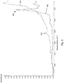
- FIG. 6 shows example FTIR spectra obtained for new and used amorphous silicon photoconductor drums.
- the top signal 601 was obtained for a new photoconductor drum which had not yet been used in a printing apparatus.
- the bottom signal 602 was obtained for a used photoconductor drum which had experienced 7 million charging cycles. It can be seen that the signal 601 for the new photoconductor drum exhibits a peak 603 at 2090 cm -1 , corresponding to the Si-H bond, which is characteristic of hydrogenated amorphous silicon.
- the signal 602 for the used photoconductor drum does not exhibit a peak at this location but instead exhibits a peak 504 at 1040 cm -1 .
- This peak 604 corresponds to the Si-OH bond, which is characteristic of an oxidation product of silicon.
- Other peaks which may be present in a FTIR spectrum for an amorphous silicon photoconductor member and which can be used in a determination of the extent of oxidation of the member are:
- a peak corresponding to an oxidation product of a material comprised in the photoconductor member is detected in the obtained spectrum.
- the photoconductor member comprises amorphous silicon
- a peak corresponding to the Si-OH bond which occurs at 1040 cm -1 . It is intended that the term "detected" can encompass both positive and negative detections. A negative detection would occur, for example, if the method was performed on a photoconductor member which was not oxidised, meaning that the obtained spectra did not contain any peaks corresponding to oxidation products.
- more than one peak is detected in the obtained spectrum.
- a peak corresponding to the Si-OH bond is detected and a peak corresponding to the Si-C bond is detected.
- an attribute of the detected peak is determined.
- block 503 comprises measuring the height of the detected peak.
- block 503 comprises calculating the area under the detected peak.
- block 503 comprises measuring the height of and/or calculating the area under each detected peak.
- block 503 comprises determining a ratio of the heights and/or areas of two of the detected peaks. In cases where no peak has been detected, the outcome of block 503 is a value of zero.
- the method also comprises, in block 504, comparing the determined attribute of the detected peak to a look-up table relating peak attribute value to extent of oxidation of the surface.
- the look-up table relates oxidation product peak height to extent of oxidation of the surface.
- the look-up table relates oxidation product peak area to extent of oxidation of the surface. It will be appreciated that the look-up table is specific to a particular photoconductor member material. A suitable look-up table may be created by obtaining spectra for photoconductor members of various usage levels, and then destructively analysing the same photoconductor members using a reference technique which permits the amount of oxidation to be determined quantitatively. EDS or XPS may be used for the quantitative analysis.
- the quantitative oxidation data can then be related to the oxidation product peak heights in a look-up table.
- a calibration graph or a correlation function relating oxidation product peak height to extent of oxidation is defined instead of or in addition to a look-up table.
- the extent of oxidation may be expressed in any of the forms described above in relation to block 102 of Figure 2 .
- the examples enable an extent of the oxidation of a photoconductor member to be determined quantitatively. This in turn enables an accurate assessment to be made regarding whether the extent of the oxidation is sufficient to affect the print quality of documents printed using that photoconductor member.
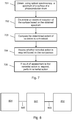
- Figure 7 shows an example of a method of assessing whether to clean the surface of a photoconductor member.
- the method comprises obtaining, using optical spectroscopy, a spectrum of a surface of a photoconductor member, block 701.
- an extent of oxidation of the surface is determined based on the obtained spectrum.
- performing blocks 701 and 702 comprises performing blocks 101 and 102 of the method shown in Figure 1 .
- performing blocks 701 and 702 comprises performing blocks 501 to 504 of the method shown in Figure 5 .
- the determined extent of oxidation of the surface of the photoconductor member is compared to a threshold.
- the threshold comprises a maximum numerical value for the amount of an oxidation product, or a component of an oxidation product, comprised in the photoconductor member. The determined extent of oxidation will be either less than, greater than, or equal to the threshold.
- block 703 comprises comparing the determined extent of oxidation of the surface of the photoconductor member to a first threshold and to a second, higher, threshold.
- block 704 whether remedial action is required is assessed based on the comparison.
- the remedial action comprises cleaning the surface of the photoconductor member and/or replacing the photoconductor member, i.e. in some examples block 704 comprises assessing whether to clean the surface of the photoconductor member, and/or assessing whether to replace the photoconductor member.
- a set of rules is defined, corresponding to the possible results of the comparison. In one example, if the extent of oxidation is less than or equal to the threshold, the result of the assessment is that remedial action is not required, and if the extent of oxidation is greater than the threshold, the result of the assessment is that remedial action is required.
- the result of the assessment is that remedial action is not required, and if the extent of oxidation is greater than or equal to the threshold, the result of the assessment is that remedial action is required.
- the result of the assessment is that remedial action is not required, if the extent of oxidation is between the first threshold and the second threshold, the result of the assessment is that cleaning of the surface of the photoconductor member is to be performed, and if the extent of oxidation is greater than the second threshold, the result of the assessment is that the photoconductor member is to be replaced.
- block 704 comprises cleaning the surface of the photoconductor member to remove some or all of the oxidation. In some such examples the RCA procedure is used to clean the surface of the photoconductor member. In some examples cleaning of the photoconductor member is instigated automatically in response to an assessment that the cleaning is to be performed. In some examples, if the result of the assessment is that the photoconductor member is to be replaced, block 704 comprises replacement of the photoconductor member.
- the method of Figure 7 is performed periodically during the operational lifetime of a given photoconductor member.
- Figure 8 shows an example of an apparatus suitable for use in performing the method of Figure 7 .
- the apparatus comprises an optical spectrometer 801.
- the optical spectrometer 801 is the same as the optical spectrometer 201 described above in relation to Figure 2 .
- the optical spectrometer 801 is the same as the optical spectrometer 304 described above in relation to Figure 3 .
- the optical spectrometer 801 is the same as the optical spectrometer 402 described above in relation to Figure 4 .
- the apparatus also comprises a processing unit 802 to receive a spectrum of a surface of a photoconductor member obtained by the optical spectrometer 801 and to determine an extent of oxidation of the surface based on the received spectrum.
- the processing unit 802 is also to assess whether to clean the surface of the photoconductor member based on the determined extent of oxidation. In some examples the processing unit 802 is also to assess whether to replace the photoconductor member based on the determined extent of oxidation.
- the apparatus also comprises a cleaning apparatus 804 to remove an oxidation product from the surface of a photoconductor member. In some examples the cleaning apparatus 804 is to perform the RCA process. In some such examples the cleaning apparatus is to immerse the photoconductor member in a plurality of chemical solutions, e.g. an ammonia-hydrogen peroxide mixed solution, a hydrochloric acid-hydrogen peroxide mixed solution, a dilute hydrofluoric acid solution. In some such examples the cleaning apparatus is to rinse and dry the photoconductor member.
- the processing unit 802 is in electronic communication, e.g. by means of a wired or wireless communications link 803, with the optical spectrometer 801.
- the processing unit 802 is also in electronic communication, e.g. by means of a wired or wireless communications link 805, with the cleaning apparatus 804.
- the processing unit is to cause the cleaning apparatus 804 to perform a cleaning process on a photoconductor member in dependence on the result of an assessment performed by the processing unit of whether the surface of the photoconductor member is to be cleaned.
- the apparatus shown in Figure 8 is integrated into a printing apparatus.
- the examples enable the operational lifetime of a photoconductor member to be significantly extended.
- Examples in the present disclosure can be provided as methods, systems or machine readable instructions, such as any combination of software, hardware, firmware or the like.
- Such machine readable instructions may be included on a computer readable storage medium (including but is not limited to disc storage, CD-ROM, optical storage, etc.) having computer readable program codes therein or thereon.
- the machine readable instructions may, for example, be executed by a general purpose computer, a special purpose computer, an embedded processor or processors of other programmable data processing devices to realize the functions described in the description and diagrams.
- a processor or processing apparatus may execute the machine readable instructions.
- functional modules of the apparatus and devices may be implemented by a processor executing machine readable instructions stored in a memory, or a processor operating in accordance with instructions embedded in logic circuitry.
- the term 'processor' is to be interpreted broadly to include a CPU, processing unit, ASIC, logic unit, or programmable gate array etc.
- the methods and functional modules may all be performed by a single processor or divided amongst several processors.
- Such machine readable instructions may also be stored in a computer readable storage that can guide the computer or other programmable data processing devices to operate in a specific mode.
- Such machine readable instructions may also be loaded onto a computer or other programmable data processing devices, so that the computer or other programmable data processing devices perform a series of operation steps to produce computer-implemented processing, thus the instructions executed on the computer or other programmable devices provide a step for realizing functions specified by flow(s) in the flow charts and/or block(s) in the block diagrams.
- teachings herein may be implemented in the form of a computer software product, the computer software product being stored in a storage medium and comprising a plurality of instructions for making a computer device implement the methods recited in the examples of the present disclosure.
Landscapes
- Physics & Mathematics (AREA)
- General Physics & Mathematics (AREA)
- Health & Medical Sciences (AREA)
- Chemical & Material Sciences (AREA)
- Immunology (AREA)
- Biochemistry (AREA)
- General Health & Medical Sciences (AREA)
- Analytical Chemistry (AREA)
- Life Sciences & Earth Sciences (AREA)
- Pathology (AREA)
- Spectroscopy & Molecular Physics (AREA)
- Nuclear Medicine, Radiotherapy & Molecular Imaging (AREA)
- Engineering & Computer Science (AREA)
- Microelectronics & Electronic Packaging (AREA)
- Chemical Kinetics & Catalysis (AREA)
- General Chemical & Material Sciences (AREA)
- Investigating, Analyzing Materials By Fluorescence Or Luminescence (AREA)
- Investigating Or Analysing Materials By Optical Means (AREA)
Claims (9)
- Verfahren, Folgendes umfassend:das Erhalten (701) eines Spektrums einer Oberfläche eines Fotoleiterelements unter Verwendung von optischer Spektroskopie, wobei sich das Fotoleiterelement während des Erhaltungsschritts in einer Druckvorrichtung befindet;das Bestimmen (702) eines Ausmaßes der Oxidation der Oberfläche basierend auf dem erhaltenen Spektrum, wobei der Bestimmungsschritt das Erfassen einer Spitze, die einem Oxidationsprodukt eines Materials entspricht, das in dem Fotoleiterelement in dem erhaltenen Spektrum enthalten ist, und das Bestimmen eines Attributs der erfassten Spitze umfasst;das Beurteilen (704), ob eine Abhilfemaßnahme erforderlich ist, basierend auf dem Vergleichen (703) des bestimmten Ausmaßes der Oxidation mit einem Schwellenwert, wobei die Abhilfemaßnahme (705) das Reinigen der Oberfläche des Fotoleiterelements durch das Entfernen des Oxidationsprodukts von der Oberfläche des Fotoleiters durch eine Reinigungsvorrichtung umfasst.
- Verfahren nach Anspruch 1, wobei der Erhaltungsschritt (701) die Verwendung von Spektroskopie mit Fourier-Transformations-Infrarot, FTIR, umfasst, um das Spektrum zu erhalten.
- Verfahren nach in Anspruch 1, wobei der Erhaltungsschritt (701) die Verwendung von Raman-Spektroskopie umfasst, um das Spektrum zu erhalten.
- Verfahren nach Anspruch 1,
wobei das bestimmte Attribut der erfassten Spitze eines von Folgenden umfasst: Spitzenhöhe, Spitzenfläche, Verhältnis der erfassten Spitzenhöhe zu der Höhe einer weiteren Spitze in dem erhaltenen Spektrum, Verhältnis der erfassten Spitzenfläche zu der Fläche einer weiteren Spitze im erhaltenen Spektrum. - Verfahren nach einem der Ansprüche 1 bis 4, wobei der Bestimmungsschritt (702) das Vergleichen des bestimmten Attributs mit einer Nachschlagetabelle umfasst, die den Wert des Oxidationsproduktattributs mit dem Ausmaß der Oxidation der Oberfläche in Verbindung bringt.
- Druckvorrichtung (403), umfassend eine Vorrichtung, wobei die Vorrichtung Folgendes umfasst:ein optisches Spektrometer (402), um ein Spektrum einer Oberfläche eines Fotoleiterelements (401) zu erhalten, wobei sich das Fotoleiterelement (401) während des Erhaltungsschritts in der Druckvorrichtung (403) befindet;eine Verarbeitungseinheit (404), die konfiguriert ist, um:ein durch das optische Spektrometer (402) erhaltenes Spektrum zu empfangen,ein Ausmaß der Oxidation der Oberfläche basierend auf dem empfangenen Spektrum zu bestimmen, wobei das Bestimmen das Erfassen einer Spitze, die einem Oxidationsprodukt eines Materials entspricht, das in dem Fotoleiterelement (401) in dem erhaltenen Spektrum enthalten ist, und das Bestimmen eines Attributs der erfassten Spitze umfasst; undzu beurteilen, ob eine Abhilfemaßnahme erforderlich ist, basierend auf dem Vergleichen des bestimmten Ausmaßes der Oxidation mit einem Schwellenwert, wobei die Abhilfemaßnahme das Reinigen der Oberfläche des Fotoleiterelements (401) durch eine Reinigungsvorrichtung umfasst; undwobei die Reinigungsvorrichtung konfiguriert ist, um die Oberfläche des Fotoleiterelements (401) durch das Entfernen eines Oxidationsprodukts von der Oberfläche des Fotoleiterelements (401) zu reinigen.
- Druckvorrichtung nach Anspruch 6, wobei das optische Spektrometer (402) einen Gelenkarm (303), der an einem Probenraum des optischen Spektrometers (402, 304) angebracht ist, und eine Messeinheit (302), die an dem Gelenkarm (303) angebracht ist, umfasst, so dass der Gelenkarm (303) einen optischen Pfad zwischen der Messeinheit (302) und dem Probenraum bereitstellt.
- Druckvorrichtung nach Anspruch 7, wobei das optische Spektrometer (402) konfiguriert ist, um ein Spektrum unter Verwendung einer abgeschwächten Totalreflexion, ATR, zu erhalten.
- Nichtflüchtiges maschinenlesbares Speichermedium, das mit Anweisungen codiert ist, die von einem Prozessor ausführbar sind, wobei das maschinenlesbare Speichermedium Folgendes umfasst:Anweisungen, um den Empfang eines Spektrums einer Oberfläche eines Fotoleiterelements, das in einer Druckvorrichtung enthalten ist, die mittels optischer Spektroskopie erhalten wird, durch den Prozessor zu erfassen, wobei das Spektrum erhalten wird, wenn sich das Fotoleiterelement in der Druckvorrichtung befindet;Anweisungen, um ein Ausmaß der Oxidation der Oberfläche des Fotoleiterelements basierend auf dem empfangenen Spektrum zu bestimmen, wobei das Bestimmen das Erfassen einer Spitze, die einem Oxidationsprodukt eines Materials entspricht, das in dem Fotoleiterelement in dem erhaltenen Spektrum enthalten ist, und das Bestimmen eines Attributs der erfassten Spitze umfasst; undAnweisungen, um zu beurteilen, ob eine Abhilfemaßnahme erforderlich ist, basierend auf dem Vergleichen des bestimmten Ausmaßes der Oxidation mit einem Schwellenwert, wobei die Abhilfemaßnahme das Reinigen der Oberfläche des Fotoleiterelements durch das Entfernen des Oxidationsprodukts von der Oberfläche des Fotoleiters durch eine Reinigungsvorrichtung umfasst.
Applications Claiming Priority (1)
| Application Number | Priority Date | Filing Date | Title |
|---|---|---|---|
| PCT/EP2015/050771 WO2016112991A1 (en) | 2015-01-16 | 2015-01-16 | Determining extent of oxidation of photoconductor surface by means of optical spectroscopy |
Publications (2)
| Publication Number | Publication Date |
|---|---|
| EP3245504A1 EP3245504A1 (de) | 2017-11-22 |
| EP3245504B1 true EP3245504B1 (de) | 2019-09-18 |
Family
ID=52350129
Family Applications (1)
| Application Number | Title | Priority Date | Filing Date |
|---|---|---|---|
| EP15700395.5A Active EP3245504B1 (de) | 2015-01-16 | 2015-01-16 | Bestimmung des ausmasses der oxidation einer photoleiteroberfläche mittels optischer spektroskopie |
Country Status (3)
| Country | Link |
|---|---|
| US (1) | US10215711B2 (de) |
| EP (1) | EP3245504B1 (de) |
| WO (1) | WO2016112991A1 (de) |
Citations (2)
| Publication number | Priority date | Publication date | Assignee | Title |
|---|---|---|---|---|
| WO2010104041A1 (ja) * | 2009-03-12 | 2010-09-16 | 三菱電機株式会社 | 薄膜太陽電池およびその製造方法 |
| CN102427097B (zh) * | 2011-11-23 | 2014-05-07 | 中国科学院物理研究所 | 一种硅的氧化钝化方法及钝化装置 |
Family Cites Families (9)
| Publication number | Priority date | Publication date | Assignee | Title |
|---|---|---|---|---|
| JP2001330977A (ja) | 2000-05-19 | 2001-11-30 | Canon Inc | 電子写真装置 |
| US6815162B2 (en) | 2001-03-12 | 2004-11-09 | National Research Council Of Canada | Passivation of porous semiconductors |
| US6818894B2 (en) * | 2001-04-30 | 2004-11-16 | The Board Of Trustees Of The University Of Illinois | Method and apparatus for characterization of ultrathin silicon oxide films using mirror-enhanced polarized reflectance fourier transform infrared spectroscopy |
| JP2007334154A (ja) | 2006-06-16 | 2007-12-27 | Kyocera Mita Corp | 画像形成方法及び画像形成装置 |
| US8180271B2 (en) | 2007-06-27 | 2012-05-15 | Ricoh Company, Ltd. | Protective layer setting unit, process cartridge, and image forming apparatus, and method of evaluating protective layer setting unit |
| JP2009069810A (ja) | 2007-08-23 | 2009-04-02 | Kyocera Mita Corp | 画像形成装置及び画像形成方法 |
| JP4764954B2 (ja) | 2009-12-28 | 2011-09-07 | キヤノン株式会社 | 電子写真感光体および電子写真装置 |
| JP2012022264A (ja) | 2010-07-16 | 2012-02-02 | Ricoh Co Ltd | 画像形成装置及び画像形成方法 |
| JP2015007753A (ja) | 2013-05-27 | 2015-01-15 | キヤノン株式会社 | 電子写真感光体 |
-
2015
- 2015-01-16 EP EP15700395.5A patent/EP3245504B1/de active Active
- 2015-01-16 WO PCT/EP2015/050771 patent/WO2016112991A1/en not_active Ceased
- 2015-01-16 US US15/521,813 patent/US10215711B2/en active Active
Patent Citations (2)
| Publication number | Priority date | Publication date | Assignee | Title |
|---|---|---|---|---|
| WO2010104041A1 (ja) * | 2009-03-12 | 2010-09-16 | 三菱電機株式会社 | 薄膜太陽電池およびその製造方法 |
| CN102427097B (zh) * | 2011-11-23 | 2014-05-07 | 中国科学院物理研究所 | 一种硅的氧化钝化方法及钝化装置 |
Non-Patent Citations (1)
| Title |
|---|
| V.E DROZD ET AL: "Study of the SiO2 layer growth by the ML-ALE method", APPLIED SURFACE SCIENCE, March 1997 (1997-03-01), pages 269 - 272, XP055530704, Retrieved from the Internet <URL:https://ac.els-cdn.com/S0169433296010185/1-s2.0-S0169433296010185-main.pdf?_tid=723b32fe-c69f-4db0-800e-15b0ca7c08a0&acdnat=1544084848_7b5f583ffe5b0d6e30873a898a378a8c> [retrieved on 20181206], DOI: 10.1016/S0169-4332(96)01018-5 * |
Also Published As
| Publication number | Publication date |
|---|---|
| US20170248527A1 (en) | 2017-08-31 |
| US10215711B2 (en) | 2019-02-26 |
| EP3245504A1 (de) | 2017-11-22 |
| WO2016112991A1 (en) | 2016-07-21 |
Similar Documents
| Publication | Publication Date | Title |
|---|---|---|
| JP5854846B2 (ja) | 画像形成装置 | |
| US10444691B2 (en) | Image forming apparatus and control program | |
| US8019239B2 (en) | Device and method for detecting life of organic photoreceptor and image forming apparatus | |
| US8948620B2 (en) | Image forming system and latent image carrier replacement time detection method | |
| US10054869B2 (en) | Image forming apparatus for detecting crack generated in charging member, method for controlling the image forming apparatus, and control program used in the image forming apparatus | |
| JP5831804B2 (ja) | 保守支援システム | |
| JP4759342B2 (ja) | 異常判定方法及び異常判定装置 | |
| JP4898478B2 (ja) | 画像形成装置 | |
| US10215711B2 (en) | Determining oxidation of photoconductor members based on obtained spectrum from optical spectroscopy | |
| JP2018146740A (ja) | 画像形成装置 | |
| US9141071B2 (en) | Image forming apparatus provided with cleaning member capable of reliably cleaning image bearing member | |
| US20130004191A1 (en) | Image forming apparatus and transfer current control method | |
| JP2019049635A (ja) | 画像形成装置 | |
| JP4788456B2 (ja) | 帯電ロール及び画像形成装置 | |
| US9753423B2 (en) | Method and device to detect negatively effected regions on an image carrier | |
| US8611769B2 (en) | Method and system for troubleshooting charging and photoreceptor failure modes associated with a xerographic process | |
| JP4734465B2 (ja) | 記録体異常発生予測装置および画像形成装置 | |
| US12130572B2 (en) | Determining the existence of defects in print apparatuses | |
| JP4642485B2 (ja) | 異常判定装置 | |
| JP6589593B2 (ja) | 少なくとも帯電および静電潜像の形成を含むプロセスに関連する構成要素の状態を評価する方法、評価プログラム、および画像形成装置 | |
| US20150098720A1 (en) | Image forming apparatus | |
| JP5473633B2 (ja) | 画像形成装置 | |
| JP2007256356A (ja) | 画像形成装置 | |
| JP2020013028A (ja) | 画像形成装置および制御プログラム | |
| JP7161701B2 (ja) | クリーニング装置、画像形成装置およびクリーニング方法 |
Legal Events
| Date | Code | Title | Description |
|---|---|---|---|
| STAA | Information on the status of an ep patent application or granted ep patent |
Free format text: STATUS: THE INTERNATIONAL PUBLICATION HAS BEEN MADE |
|
| PUAI | Public reference made under article 153(3) epc to a published international application that has entered the european phase |
Free format text: ORIGINAL CODE: 0009012 |
|
| STAA | Information on the status of an ep patent application or granted ep patent |
Free format text: STATUS: REQUEST FOR EXAMINATION WAS MADE |
|
| 17P | Request for examination filed |
Effective date: 20170413 |
|
| AK | Designated contracting states |
Kind code of ref document: A1 Designated state(s): AL AT BE BG CH CY CZ DE DK EE ES FI FR GB GR HR HU IE IS IT LI LT LU LV MC MK MT NL NO PL PT RO RS SE SI SK SM TR |
|
| AX | Request for extension of the european patent |
Extension state: BA ME |
|
| RAP1 | Party data changed (applicant data changed or rights of an application transferred) |
Owner name: HP INDIGO B.V. |
|
| DAX | Request for extension of the european patent (deleted) | ||
| STAA | Information on the status of an ep patent application or granted ep patent |
Free format text: STATUS: EXAMINATION IS IN PROGRESS |
|
| 17Q | First examination report despatched |
Effective date: 20181211 |
|
| REG | Reference to a national code |
Ref country code: DE Ref legal event code: R079 Ref document number: 602015038163 Country of ref document: DE Free format text: PREVIOUS MAIN CLASS: G01N0021356300 Ipc: G01N0021650000 |
|
| GRAP | Despatch of communication of intention to grant a patent |
Free format text: ORIGINAL CODE: EPIDOSNIGR1 |
|
| STAA | Information on the status of an ep patent application or granted ep patent |
Free format text: STATUS: GRANT OF PATENT IS INTENDED |
|
| RIC1 | Information provided on ipc code assigned before grant |
Ipc: G01N 21/65 20060101AFI20190517BHEP Ipc: G01N 21/35 20140101ALN20190517BHEP Ipc: G03G 21/00 20060101ALI20190517BHEP Ipc: G01N 21/3563 20140101ALI20190517BHEP Ipc: G03G 15/00 20060101ALI20190517BHEP |
|
| INTG | Intention to grant announced |
Effective date: 20190614 |
|
| GRAS | Grant fee paid |
Free format text: ORIGINAL CODE: EPIDOSNIGR3 |
|
| GRAA | (expected) grant |
Free format text: ORIGINAL CODE: 0009210 |
|
| STAA | Information on the status of an ep patent application or granted ep patent |
Free format text: STATUS: THE PATENT HAS BEEN GRANTED |
|
| AK | Designated contracting states |
Kind code of ref document: B1 Designated state(s): AL AT BE BG CH CY CZ DE DK EE ES FI FR GB GR HR HU IE IS IT LI LT LU LV MC MK MT NL NO PL PT RO RS SE SI SK SM TR |
|
| REG | Reference to a national code |
Ref country code: GB Ref legal event code: FG4D |
|
| REG | Reference to a national code |
Ref country code: CH Ref legal event code: EP |
|
| REG | Reference to a national code |
Ref country code: DE Ref legal event code: R096 Ref document number: 602015038163 Country of ref document: DE |
|
| REG | Reference to a national code |
Ref country code: AT Ref legal event code: REF Ref document number: 1181919 Country of ref document: AT Kind code of ref document: T Effective date: 20191015 |
|
| REG | Reference to a national code |
Ref country code: IE Ref legal event code: FG4D |
|
| REG | Reference to a national code |
Ref country code: NL Ref legal event code: MP Effective date: 20190918 |
|
| PG25 | Lapsed in a contracting state [announced via postgrant information from national office to epo] |
Ref country code: SE Free format text: LAPSE BECAUSE OF FAILURE TO SUBMIT A TRANSLATION OF THE DESCRIPTION OR TO PAY THE FEE WITHIN THE PRESCRIBED TIME-LIMIT Effective date: 20190918 Ref country code: BG Free format text: LAPSE BECAUSE OF FAILURE TO SUBMIT A TRANSLATION OF THE DESCRIPTION OR TO PAY THE FEE WITHIN THE PRESCRIBED TIME-LIMIT Effective date: 20191218 Ref country code: NO Free format text: LAPSE BECAUSE OF FAILURE TO SUBMIT A TRANSLATION OF THE DESCRIPTION OR TO PAY THE FEE WITHIN THE PRESCRIBED TIME-LIMIT Effective date: 20191218 Ref country code: LT Free format text: LAPSE BECAUSE OF FAILURE TO SUBMIT A TRANSLATION OF THE DESCRIPTION OR TO PAY THE FEE WITHIN THE PRESCRIBED TIME-LIMIT Effective date: 20190918 Ref country code: HR Free format text: LAPSE BECAUSE OF FAILURE TO SUBMIT A TRANSLATION OF THE DESCRIPTION OR TO PAY THE FEE WITHIN THE PRESCRIBED TIME-LIMIT Effective date: 20190918 Ref country code: FI Free format text: LAPSE BECAUSE OF FAILURE TO SUBMIT A TRANSLATION OF THE DESCRIPTION OR TO PAY THE FEE WITHIN THE PRESCRIBED TIME-LIMIT Effective date: 20190918 |
|
| REG | Reference to a national code |
Ref country code: LT Ref legal event code: MG4D |
|
| PG25 | Lapsed in a contracting state [announced via postgrant information from national office to epo] |
Ref country code: LV Free format text: LAPSE BECAUSE OF FAILURE TO SUBMIT A TRANSLATION OF THE DESCRIPTION OR TO PAY THE FEE WITHIN THE PRESCRIBED TIME-LIMIT Effective date: 20190918 Ref country code: AL Free format text: LAPSE BECAUSE OF FAILURE TO SUBMIT A TRANSLATION OF THE DESCRIPTION OR TO PAY THE FEE WITHIN THE PRESCRIBED TIME-LIMIT Effective date: 20190918 Ref country code: RS Free format text: LAPSE BECAUSE OF FAILURE TO SUBMIT A TRANSLATION OF THE DESCRIPTION OR TO PAY THE FEE WITHIN THE PRESCRIBED TIME-LIMIT Effective date: 20190918 Ref country code: GR Free format text: LAPSE BECAUSE OF FAILURE TO SUBMIT A TRANSLATION OF THE DESCRIPTION OR TO PAY THE FEE WITHIN THE PRESCRIBED TIME-LIMIT Effective date: 20191219 |
|
| REG | Reference to a national code |
Ref country code: AT Ref legal event code: MK05 Ref document number: 1181919 Country of ref document: AT Kind code of ref document: T Effective date: 20190918 |
|
| PG25 | Lapsed in a contracting state [announced via postgrant information from national office to epo] |
Ref country code: ES Free format text: LAPSE BECAUSE OF FAILURE TO SUBMIT A TRANSLATION OF THE DESCRIPTION OR TO PAY THE FEE WITHIN THE PRESCRIBED TIME-LIMIT Effective date: 20190918 Ref country code: AT Free format text: LAPSE BECAUSE OF FAILURE TO SUBMIT A TRANSLATION OF THE DESCRIPTION OR TO PAY THE FEE WITHIN THE PRESCRIBED TIME-LIMIT Effective date: 20190918 Ref country code: PL Free format text: LAPSE BECAUSE OF FAILURE TO SUBMIT A TRANSLATION OF THE DESCRIPTION OR TO PAY THE FEE WITHIN THE PRESCRIBED TIME-LIMIT Effective date: 20190918 Ref country code: RO Free format text: LAPSE BECAUSE OF FAILURE TO SUBMIT A TRANSLATION OF THE DESCRIPTION OR TO PAY THE FEE WITHIN THE PRESCRIBED TIME-LIMIT Effective date: 20190918 Ref country code: NL Free format text: LAPSE BECAUSE OF FAILURE TO SUBMIT A TRANSLATION OF THE DESCRIPTION OR TO PAY THE FEE WITHIN THE PRESCRIBED TIME-LIMIT Effective date: 20190918 Ref country code: IT Free format text: LAPSE BECAUSE OF FAILURE TO SUBMIT A TRANSLATION OF THE DESCRIPTION OR TO PAY THE FEE WITHIN THE PRESCRIBED TIME-LIMIT Effective date: 20190918 Ref country code: EE Free format text: LAPSE BECAUSE OF FAILURE TO SUBMIT A TRANSLATION OF THE DESCRIPTION OR TO PAY THE FEE WITHIN THE PRESCRIBED TIME-LIMIT Effective date: 20190918 Ref country code: PT Free format text: LAPSE BECAUSE OF FAILURE TO SUBMIT A TRANSLATION OF THE DESCRIPTION OR TO PAY THE FEE WITHIN THE PRESCRIBED TIME-LIMIT Effective date: 20200120 |
|
| PG25 | Lapsed in a contracting state [announced via postgrant information from national office to epo] |
Ref country code: SM Free format text: LAPSE BECAUSE OF FAILURE TO SUBMIT A TRANSLATION OF THE DESCRIPTION OR TO PAY THE FEE WITHIN THE PRESCRIBED TIME-LIMIT Effective date: 20190918 Ref country code: IS Free format text: LAPSE BECAUSE OF FAILURE TO SUBMIT A TRANSLATION OF THE DESCRIPTION OR TO PAY THE FEE WITHIN THE PRESCRIBED TIME-LIMIT Effective date: 20200224 Ref country code: CZ Free format text: LAPSE BECAUSE OF FAILURE TO SUBMIT A TRANSLATION OF THE DESCRIPTION OR TO PAY THE FEE WITHIN THE PRESCRIBED TIME-LIMIT Effective date: 20190918 Ref country code: SK Free format text: LAPSE BECAUSE OF FAILURE TO SUBMIT A TRANSLATION OF THE DESCRIPTION OR TO PAY THE FEE WITHIN THE PRESCRIBED TIME-LIMIT Effective date: 20190918 |
|
| REG | Reference to a national code |
Ref country code: DE Ref legal event code: R097 Ref document number: 602015038163 Country of ref document: DE |
|
| PLBE | No opposition filed within time limit |
Free format text: ORIGINAL CODE: 0009261 |
|
| STAA | Information on the status of an ep patent application or granted ep patent |
Free format text: STATUS: NO OPPOSITION FILED WITHIN TIME LIMIT |
|
| PG2D | Information on lapse in contracting state deleted |
Ref country code: IS |
|
| PG25 | Lapsed in a contracting state [announced via postgrant information from national office to epo] |
Ref country code: DK Free format text: LAPSE BECAUSE OF FAILURE TO SUBMIT A TRANSLATION OF THE DESCRIPTION OR TO PAY THE FEE WITHIN THE PRESCRIBED TIME-LIMIT Effective date: 20190918 Ref country code: IS Free format text: LAPSE BECAUSE OF FAILURE TO SUBMIT A TRANSLATION OF THE DESCRIPTION OR TO PAY THE FEE WITHIN THE PRESCRIBED TIME-LIMIT Effective date: 20200119 |
|
| 26N | No opposition filed |
Effective date: 20200619 |
|
| PG25 | Lapsed in a contracting state [announced via postgrant information from national office to epo] |
Ref country code: MC Free format text: LAPSE BECAUSE OF FAILURE TO SUBMIT A TRANSLATION OF THE DESCRIPTION OR TO PAY THE FEE WITHIN THE PRESCRIBED TIME-LIMIT Effective date: 20190918 Ref country code: SI Free format text: LAPSE BECAUSE OF FAILURE TO SUBMIT A TRANSLATION OF THE DESCRIPTION OR TO PAY THE FEE WITHIN THE PRESCRIBED TIME-LIMIT Effective date: 20190918 |
|
| REG | Reference to a national code |
Ref country code: CH Ref legal event code: PL |
|
| REG | Reference to a national code |
Ref country code: BE Ref legal event code: MM Effective date: 20200131 |
|
| PG25 | Lapsed in a contracting state [announced via postgrant information from national office to epo] |
Ref country code: LU Free format text: LAPSE BECAUSE OF NON-PAYMENT OF DUE FEES Effective date: 20200116 |
|
| PG25 | Lapsed in a contracting state [announced via postgrant information from national office to epo] |
Ref country code: LI Free format text: LAPSE BECAUSE OF NON-PAYMENT OF DUE FEES Effective date: 20200131 Ref country code: CH Free format text: LAPSE BECAUSE OF NON-PAYMENT OF DUE FEES Effective date: 20200131 Ref country code: BE Free format text: LAPSE BECAUSE OF NON-PAYMENT OF DUE FEES Effective date: 20200131 |
|
| PG25 | Lapsed in a contracting state [announced via postgrant information from national office to epo] |
Ref country code: IE Free format text: LAPSE BECAUSE OF NON-PAYMENT OF DUE FEES Effective date: 20200116 |
|
| PGFP | Annual fee paid to national office [announced via postgrant information from national office to epo] |
Ref country code: FR Payment date: 20211215 Year of fee payment: 8 Ref country code: GB Payment date: 20211216 Year of fee payment: 8 |
|
| PG25 | Lapsed in a contracting state [announced via postgrant information from national office to epo] |
Ref country code: TR Free format text: LAPSE BECAUSE OF FAILURE TO SUBMIT A TRANSLATION OF THE DESCRIPTION OR TO PAY THE FEE WITHIN THE PRESCRIBED TIME-LIMIT Effective date: 20190918 Ref country code: MT Free format text: LAPSE BECAUSE OF FAILURE TO SUBMIT A TRANSLATION OF THE DESCRIPTION OR TO PAY THE FEE WITHIN THE PRESCRIBED TIME-LIMIT Effective date: 20190918 Ref country code: CY Free format text: LAPSE BECAUSE OF FAILURE TO SUBMIT A TRANSLATION OF THE DESCRIPTION OR TO PAY THE FEE WITHIN THE PRESCRIBED TIME-LIMIT Effective date: 20190918 |
|
| PG25 | Lapsed in a contracting state [announced via postgrant information from national office to epo] |
Ref country code: MK Free format text: LAPSE BECAUSE OF FAILURE TO SUBMIT A TRANSLATION OF THE DESCRIPTION OR TO PAY THE FEE WITHIN THE PRESCRIBED TIME-LIMIT Effective date: 20190918 |
|
| GBPC | Gb: european patent ceased through non-payment of renewal fee |
Effective date: 20230116 |
|
| PG25 | Lapsed in a contracting state [announced via postgrant information from national office to epo] |
Ref country code: GB Free format text: LAPSE BECAUSE OF NON-PAYMENT OF DUE FEES Effective date: 20230116 |
|
| PG25 | Lapsed in a contracting state [announced via postgrant information from national office to epo] |
Ref country code: FR Free format text: LAPSE BECAUSE OF NON-PAYMENT OF DUE FEES Effective date: 20230131 |
|
| PGFP | Annual fee paid to national office [announced via postgrant information from national office to epo] |
Ref country code: DE Payment date: 20251217 Year of fee payment: 12 |