EP3233733B1 - Composants électroniques améliorés à nanotubes de nitrure de bore - Google Patents
Composants électroniques améliorés à nanotubes de nitrure de bore Download PDFInfo
- Publication number
- EP3233733B1 EP3233733B1 EP15871103.6A EP15871103A EP3233733B1 EP 3233733 B1 EP3233733 B1 EP 3233733B1 EP 15871103 A EP15871103 A EP 15871103A EP 3233733 B1 EP3233733 B1 EP 3233733B1
- Authority
- EP
- European Patent Office
- Prior art keywords
- bnnt
- bnnts
- layer
- group layer
- contact surface
- Prior art date
- Legal status (The legal status is an assumption and is not a legal conclusion. Google has not performed a legal analysis and makes no representation as to the accuracy of the status listed.)
- Active
Links
- PZNSFCLAULLKQX-UHFFFAOYSA-N Boron nitride Chemical compound N#B PZNSFCLAULLKQX-UHFFFAOYSA-N 0.000 title claims description 163
- 229910052582 BN Inorganic materials 0.000 title claims description 11
- 239000002071 nanotube Substances 0.000 title claims description 11
- 239000000463 material Substances 0.000 claims description 112
- 229920000642 polymer Polymers 0.000 claims description 14
- 239000000919 ceramic Substances 0.000 claims description 13
- 229910052751 metal Inorganic materials 0.000 claims description 13
- 239000002184 metal Substances 0.000 claims description 13
- 239000004593 Epoxy Substances 0.000 claims description 8
- 239000004020 conductor Substances 0.000 claims description 7
- 239000004519 grease Substances 0.000 claims description 5
- 238000001802 infusion Methods 0.000 claims description 4
- 239000010410 layer Substances 0.000 description 110
- 238000000034 method Methods 0.000 description 36
- 230000032258 transport Effects 0.000 description 23
- 239000000835 fiber Substances 0.000 description 22
- 230000008569 process Effects 0.000 description 20
- 239000002131 composite material Substances 0.000 description 15
- 238000004519 manufacturing process Methods 0.000 description 12
- OKTJSMMVPCPJKN-UHFFFAOYSA-N Carbon Chemical compound [C] OKTJSMMVPCPJKN-UHFFFAOYSA-N 0.000 description 10
- 239000012535 impurity Substances 0.000 description 9
- 239000002245 particle Substances 0.000 description 9
- 239000004065 semiconductor Substances 0.000 description 9
- 230000015572 biosynthetic process Effects 0.000 description 8
- ZOXJGFHDIHLPTG-UHFFFAOYSA-N Boron Chemical compound [B] ZOXJGFHDIHLPTG-UHFFFAOYSA-N 0.000 description 7
- 230000002708 enhancing effect Effects 0.000 description 6
- 239000003292 glue Substances 0.000 description 6
- 238000003786 synthesis reaction Methods 0.000 description 6
- 239000003990 capacitor Substances 0.000 description 5
- 239000002041 carbon nanotube Substances 0.000 description 5
- 238000005229 chemical vapour deposition Methods 0.000 description 5
- 238000000576 coating method Methods 0.000 description 5
- 230000007547 defect Effects 0.000 description 5
- 239000004744 fabric Substances 0.000 description 5
- 239000011229 interlayer Substances 0.000 description 5
- 238000012546 transfer Methods 0.000 description 5
- LFQSCWFLJHTTHZ-UHFFFAOYSA-N Ethanol Chemical compound CCO LFQSCWFLJHTTHZ-UHFFFAOYSA-N 0.000 description 4
- 229910052796 boron Inorganic materials 0.000 description 4
- 239000003054 catalyst Substances 0.000 description 4
- -1 few walls Chemical compound 0.000 description 4
- 229910021389 graphene Inorganic materials 0.000 description 4
- 238000010438 heat treatment Methods 0.000 description 4
- 150000002739 metals Chemical class 0.000 description 4
- 238000009941 weaving Methods 0.000 description 4
- 235000009161 Espostoa lanata Nutrition 0.000 description 3
- 240000001624 Espostoa lanata Species 0.000 description 3
- YXFVVABEGXRONW-UHFFFAOYSA-N Toluene Chemical compound CC1=CC=CC=C1 YXFVVABEGXRONW-UHFFFAOYSA-N 0.000 description 3
- 229910052782 aluminium Inorganic materials 0.000 description 3
- XAGFODPZIPBFFR-UHFFFAOYSA-N aluminium Chemical compound [Al] XAGFODPZIPBFFR-UHFFFAOYSA-N 0.000 description 3
- 230000009286 beneficial effect Effects 0.000 description 3
- 229910021393 carbon nanotube Inorganic materials 0.000 description 3
- 239000011248 coating agent Substances 0.000 description 3
- 230000006835 compression Effects 0.000 description 3
- 238000007906 compression Methods 0.000 description 3
- 230000001419 dependent effect Effects 0.000 description 3
- 239000002270 dispersing agent Substances 0.000 description 3
- 238000009826 distribution Methods 0.000 description 3
- 235000019441 ethanol Nutrition 0.000 description 3
- PCHJSUWPFVWCPO-UHFFFAOYSA-N gold Chemical compound [Au] PCHJSUWPFVWCPO-UHFFFAOYSA-N 0.000 description 3
- 229910052737 gold Inorganic materials 0.000 description 3
- 239000010931 gold Substances 0.000 description 3
- 229910002804 graphite Inorganic materials 0.000 description 3
- 239000010439 graphite Substances 0.000 description 3
- 238000010348 incorporation Methods 0.000 description 3
- 229910000679 solder Inorganic materials 0.000 description 3
- 239000000126 substance Substances 0.000 description 3
- IJGRMHOSHXDMSA-UHFFFAOYSA-N Atomic nitrogen Chemical compound N#N IJGRMHOSHXDMSA-UHFFFAOYSA-N 0.000 description 2
- RYGMFSIKBFXOCR-UHFFFAOYSA-N Copper Chemical compound [Cu] RYGMFSIKBFXOCR-UHFFFAOYSA-N 0.000 description 2
- HBBGRARXTFLTSG-UHFFFAOYSA-N Lithium ion Chemical compound [Li+] HBBGRARXTFLTSG-UHFFFAOYSA-N 0.000 description 2
- 238000001069 Raman spectroscopy Methods 0.000 description 2
- VYPSYNLAJGMNEJ-UHFFFAOYSA-N Silicium dioxide Chemical compound O=[Si]=O VYPSYNLAJGMNEJ-UHFFFAOYSA-N 0.000 description 2
- 230000008901 benefit Effects 0.000 description 2
- 238000006243 chemical reaction Methods 0.000 description 2
- 229910052802 copper Inorganic materials 0.000 description 2
- 239000010949 copper Substances 0.000 description 2
- 230000003247 decreasing effect Effects 0.000 description 2
- 238000000578 dry spinning Methods 0.000 description 2
- 238000010894 electron beam technology Methods 0.000 description 2
- 238000005516 engineering process Methods 0.000 description 2
- 238000001914 filtration Methods 0.000 description 2
- 239000007789 gas Substances 0.000 description 2
- 239000011810 insulating material Substances 0.000 description 2
- 230000003993 interaction Effects 0.000 description 2
- 238000010884 ion-beam technique Methods 0.000 description 2
- 239000007788 liquid Substances 0.000 description 2
- 229910001416 lithium ion Inorganic materials 0.000 description 2
- 238000002844 melting Methods 0.000 description 2
- 230000008018 melting Effects 0.000 description 2
- 239000000615 nonconductor Substances 0.000 description 2
- 239000002861 polymer material Substances 0.000 description 2
- 238000000746 purification Methods 0.000 description 2
- 210000002268 wool Anatomy 0.000 description 2
- 229910002704 AlGaN Inorganic materials 0.000 description 1
- 229910002601 GaN Inorganic materials 0.000 description 1
- 229910000530 Gallium indium arsenide Inorganic materials 0.000 description 1
- 206010028980 Neoplasm Diseases 0.000 description 1
- OAICVXFJPJFONN-UHFFFAOYSA-N Phosphorus Chemical compound [P] OAICVXFJPJFONN-UHFFFAOYSA-N 0.000 description 1
- 238000005411 Van der Waals force Methods 0.000 description 1
- 230000001133 acceleration Effects 0.000 description 1
- PNEYBMLMFCGWSK-UHFFFAOYSA-N aluminium oxide Inorganic materials [O-2].[O-2].[O-2].[Al+3].[Al+3] PNEYBMLMFCGWSK-UHFFFAOYSA-N 0.000 description 1
- 201000011510 cancer Diseases 0.000 description 1
- 238000001311 chemical methods and process Methods 0.000 description 1
- 229910052681 coesite Inorganic materials 0.000 description 1
- 238000001816 cooling Methods 0.000 description 1
- 229910052593 corundum Inorganic materials 0.000 description 1
- 229910052906 cristobalite Inorganic materials 0.000 description 1
- 239000003989 dielectric material Substances 0.000 description 1
- 230000003467 diminishing effect Effects 0.000 description 1
- 239000012777 electrically insulating material Substances 0.000 description 1
- 238000004520 electroporation Methods 0.000 description 1
- 125000003700 epoxy group Chemical group 0.000 description 1
- 239000012530 fluid Substances 0.000 description 1
- 229910052732 germanium Inorganic materials 0.000 description 1
- 239000011521 glass Substances 0.000 description 1
- 230000020169 heat generation Effects 0.000 description 1
- 238000012423 maintenance Methods 0.000 description 1
- 238000010297 mechanical methods and process Methods 0.000 description 1
- 230000005226 mechanical processes and functions Effects 0.000 description 1
- 230000007246 mechanism Effects 0.000 description 1
- 239000000155 melt Substances 0.000 description 1
- 239000012528 membrane Substances 0.000 description 1
- 229910052757 nitrogen Inorganic materials 0.000 description 1
- 230000001590 oxidative effect Effects 0.000 description 1
- 229920000647 polyepoxide Polymers 0.000 description 1
- 238000012545 processing Methods 0.000 description 1
- 229910052594 sapphire Inorganic materials 0.000 description 1
- 239000010980 sapphire Substances 0.000 description 1
- 229910052710 silicon Inorganic materials 0.000 description 1
- 239000000377 silicon dioxide Substances 0.000 description 1
- LIVNPJMFVYWSIS-UHFFFAOYSA-N silicon monoxide Inorganic materials [Si-]#[O+] LIVNPJMFVYWSIS-UHFFFAOYSA-N 0.000 description 1
- 238000005245 sintering Methods 0.000 description 1
- 239000011343 solid material Substances 0.000 description 1
- 238000000527 sonication Methods 0.000 description 1
- 238000003892 spreading Methods 0.000 description 1
- 230000007480 spreading Effects 0.000 description 1
- 229910052682 stishovite Inorganic materials 0.000 description 1
- 239000000758 substrate Substances 0.000 description 1
- 239000004094 surface-active agent Substances 0.000 description 1
- 238000005382 thermal cycling Methods 0.000 description 1
- 230000007704 transition Effects 0.000 description 1
- 239000012780 transparent material Substances 0.000 description 1
- 229910052905 tridymite Inorganic materials 0.000 description 1
- XLYOFNOQVPJJNP-UHFFFAOYSA-N water Substances O XLYOFNOQVPJJNP-UHFFFAOYSA-N 0.000 description 1
- 239000002759 woven fabric Substances 0.000 description 1
- 229910001845 yogo sapphire Inorganic materials 0.000 description 1
Images


Classifications
-
- H—ELECTRICITY
- H01—ELECTRIC ELEMENTS
- H01L—SEMICONDUCTOR DEVICES NOT COVERED BY CLASS H10
- H01L23/00—Details of semiconductor or other solid state devices
- H01L23/34—Arrangements for cooling, heating, ventilating or temperature compensation ; Temperature sensing arrangements
- H01L23/36—Selection of materials, or shaping, to facilitate cooling or heating, e.g. heatsinks
- H01L23/373—Cooling facilitated by selection of materials for the device or materials for thermal expansion adaptation, e.g. carbon
- H01L23/3733—Cooling facilitated by selection of materials for the device or materials for thermal expansion adaptation, e.g. carbon having a heterogeneous or anisotropic structure, e.g. powder or fibres in a matrix, wire mesh, porous structures
-
- C—CHEMISTRY; METALLURGY
- C01—INORGANIC CHEMISTRY
- C01B—NON-METALLIC ELEMENTS; COMPOUNDS THEREOF; METALLOIDS OR COMPOUNDS THEREOF NOT COVERED BY SUBCLASS C01C
- C01B21/00—Nitrogen; Compounds thereof
- C01B21/06—Binary compounds of nitrogen with metals, with silicon, or with boron, or with carbon, i.e. nitrides; Compounds of nitrogen with more than one metal, silicon or boron
- C01B21/064—Binary compounds of nitrogen with metals, with silicon, or with boron, or with carbon, i.e. nitrides; Compounds of nitrogen with more than one metal, silicon or boron with boron
- C01B21/0648—After-treatment, e.g. grinding, purification
-
- C—CHEMISTRY; METALLURGY
- C09—DYES; PAINTS; POLISHES; NATURAL RESINS; ADHESIVES; COMPOSITIONS NOT OTHERWISE PROVIDED FOR; APPLICATIONS OF MATERIALS NOT OTHERWISE PROVIDED FOR
- C09K—MATERIALS FOR MISCELLANEOUS APPLICATIONS, NOT PROVIDED FOR ELSEWHERE
- C09K5/00—Heat-transfer, heat-exchange or heat-storage materials, e.g. refrigerants; Materials for the production of heat or cold by chemical reactions other than by combustion
- C09K5/08—Materials not undergoing a change of physical state when used
- C09K5/14—Solid materials, e.g. powdery or granular
-
- H—ELECTRICITY
- H01—ELECTRIC ELEMENTS
- H01L—SEMICONDUCTOR DEVICES NOT COVERED BY CLASS H10
- H01L23/00—Details of semiconductor or other solid state devices
- H01L23/34—Arrangements for cooling, heating, ventilating or temperature compensation ; Temperature sensing arrangements
- H01L23/36—Selection of materials, or shaping, to facilitate cooling or heating, e.g. heatsinks
- H01L23/373—Cooling facilitated by selection of materials for the device or materials for thermal expansion adaptation, e.g. carbon
- H01L23/3731—Ceramic materials or glass
-
- H—ELECTRICITY
- H01—ELECTRIC ELEMENTS
- H01L—SEMICONDUCTOR DEVICES NOT COVERED BY CLASS H10
- H01L23/00—Details of semiconductor or other solid state devices
- H01L23/34—Arrangements for cooling, heating, ventilating or temperature compensation ; Temperature sensing arrangements
- H01L23/36—Selection of materials, or shaping, to facilitate cooling or heating, e.g. heatsinks
- H01L23/373—Cooling facilitated by selection of materials for the device or materials for thermal expansion adaptation, e.g. carbon
- H01L23/3736—Metallic materials
-
- H—ELECTRICITY
- H01—ELECTRIC ELEMENTS
- H01L—SEMICONDUCTOR DEVICES NOT COVERED BY CLASS H10
- H01L23/00—Details of semiconductor or other solid state devices
- H01L23/34—Arrangements for cooling, heating, ventilating or temperature compensation ; Temperature sensing arrangements
- H01L23/36—Selection of materials, or shaping, to facilitate cooling or heating, e.g. heatsinks
- H01L23/373—Cooling facilitated by selection of materials for the device or materials for thermal expansion adaptation, e.g. carbon
- H01L23/3737—Organic materials with or without a thermoconductive filler
-
- H—ELECTRICITY
- H01—ELECTRIC ELEMENTS
- H01L—SEMICONDUCTOR DEVICES NOT COVERED BY CLASS H10
- H01L33/00—Semiconductor devices with at least one potential-jump barrier or surface barrier specially adapted for light emission; Processes or apparatus specially adapted for the manufacture or treatment thereof or of parts thereof; Details thereof
- H01L33/48—Semiconductor devices with at least one potential-jump barrier or surface barrier specially adapted for light emission; Processes or apparatus specially adapted for the manufacture or treatment thereof or of parts thereof; Details thereof characterised by the semiconductor body packages
- H01L33/64—Heat extraction or cooling elements
- H01L33/641—Heat extraction or cooling elements characterized by the materials
-
- B—PERFORMING OPERATIONS; TRANSPORTING
- B82—NANOTECHNOLOGY
- B82Y—SPECIFIC USES OR APPLICATIONS OF NANOSTRUCTURES; MEASUREMENT OR ANALYSIS OF NANOSTRUCTURES; MANUFACTURE OR TREATMENT OF NANOSTRUCTURES
- B82Y30/00—Nanotechnology for materials or surface science, e.g. nanocomposites
-
- B—PERFORMING OPERATIONS; TRANSPORTING
- B82—NANOTECHNOLOGY
- B82Y—SPECIFIC USES OR APPLICATIONS OF NANOSTRUCTURES; MEASUREMENT OR ANALYSIS OF NANOSTRUCTURES; MANUFACTURE OR TREATMENT OF NANOSTRUCTURES
- B82Y40/00—Manufacture or treatment of nanostructures
-
- C—CHEMISTRY; METALLURGY
- C01—INORGANIC CHEMISTRY
- C01P—INDEXING SCHEME RELATING TO STRUCTURAL AND PHYSICAL ASPECTS OF SOLID INORGANIC COMPOUNDS
- C01P2004/00—Particle morphology
- C01P2004/10—Particle morphology extending in one dimension, e.g. needle-like
- C01P2004/13—Nanotubes
-
- C—CHEMISTRY; METALLURGY
- C01—INORGANIC CHEMISTRY
- C01P—INDEXING SCHEME RELATING TO STRUCTURAL AND PHYSICAL ASPECTS OF SOLID INORGANIC COMPOUNDS
- C01P2006/00—Physical properties of inorganic compounds
- C01P2006/32—Thermal properties
-
- H—ELECTRICITY
- H01—ELECTRIC ELEMENTS
- H01L—SEMICONDUCTOR DEVICES NOT COVERED BY CLASS H10
- H01L2924/00—Indexing scheme for arrangements or methods for connecting or disconnecting semiconductor or solid-state bodies as covered by H01L24/00
- H01L2924/0001—Technical content checked by a classifier
- H01L2924/0002—Not covered by any one of groups H01L24/00, H01L24/00 and H01L2224/00
-
- Y—GENERAL TAGGING OF NEW TECHNOLOGICAL DEVELOPMENTS; GENERAL TAGGING OF CROSS-SECTIONAL TECHNOLOGIES SPANNING OVER SEVERAL SECTIONS OF THE IPC; TECHNICAL SUBJECTS COVERED BY FORMER USPC CROSS-REFERENCE ART COLLECTIONS [XRACs] AND DIGESTS
- Y10—TECHNICAL SUBJECTS COVERED BY FORMER USPC
- Y10S—TECHNICAL SUBJECTS COVERED BY FORMER USPC CROSS-REFERENCE ART COLLECTIONS [XRACs] AND DIGESTS
- Y10S977/00—Nanotechnology
- Y10S977/70—Nanostructure
- Y10S977/734—Fullerenes, i.e. graphene-based structures, such as nanohorns, nanococoons, nanoscrolls or fullerene-like structures, e.g. WS2 or MoS2 chalcogenide nanotubes, planar C3N4, etc.
-
- Y—GENERAL TAGGING OF NEW TECHNOLOGICAL DEVELOPMENTS; GENERAL TAGGING OF CROSS-SECTIONAL TECHNOLOGIES SPANNING OVER SEVERAL SECTIONS OF THE IPC; TECHNICAL SUBJECTS COVERED BY FORMER USPC CROSS-REFERENCE ART COLLECTIONS [XRACs] AND DIGESTS
- Y10—TECHNICAL SUBJECTS COVERED BY FORMER USPC
- Y10S—TECHNICAL SUBJECTS COVERED BY FORMER USPC CROSS-REFERENCE ART COLLECTIONS [XRACs] AND DIGESTS
- Y10S977/00—Nanotechnology
- Y10S977/84—Manufacture, treatment, or detection of nanostructure
- Y10S977/89—Deposition of materials, e.g. coating, cvd, or ald
- Y10S977/892—Liquid phase deposition
-
- Y—GENERAL TAGGING OF NEW TECHNOLOGICAL DEVELOPMENTS; GENERAL TAGGING OF CROSS-SECTIONAL TECHNOLOGIES SPANNING OVER SEVERAL SECTIONS OF THE IPC; TECHNICAL SUBJECTS COVERED BY FORMER USPC CROSS-REFERENCE ART COLLECTIONS [XRACs] AND DIGESTS
- Y10—TECHNICAL SUBJECTS COVERED BY FORMER USPC
- Y10S—TECHNICAL SUBJECTS COVERED BY FORMER USPC CROSS-REFERENCE ART COLLECTIONS [XRACs] AND DIGESTS
- Y10S977/00—Nanotechnology
- Y10S977/902—Specified use of nanostructure
- Y10S977/932—Specified use of nanostructure for electronic or optoelectronic application
Definitions
- the present disclosure generally relates to enhancing the performance of electronic components through the inclusion of boron nitride nanotubes.
- EC electronic components
- LEDs light emitting diodes
- integrated circuits integrated circuits
- multilayer integrated circuits As electronic components (ECs), such as diodes, light emitting diodes (LEDs), transistors, integrated circuits and multilayer integrated circuits, EC performance becomes more critical. In most instances, EC performance is frequently limited by the EC's stability to minimize heat production and improve heat transport away from the heat generating regions to heat sinks, thereby keeping the junction temperatures and component temperatures low and diminishing thermally-generated mechanical stresses in the materials and layers making up the EC.
- the diodes, transistors, etc. in ECs all have a certain amount of electrical resistance. When electrical currents flow in the ECs, heat is generated. One parameter of importance is the junction temperature, where one type of semiconductor interfaces with another type of semiconductor. This is also the location where much of the resistance is located. Heat generated at these locations impacts the performance including lifetime of the EC. Removing this heat and keeping the junction temperatures as low as possible is important for proper functioning of the EC.
- Carbon nanotubes (CNTs), graphene and pyrolytic graphite can be incorporated in ECs where electrically conductive and/or semi conductive properties are desired.
- CNTs and graphene can also favorably affect heat transport and structural strength. However, they do not work where the material needs to be electrically insulating. Thus, CNTs have limited efficacy with respect to enhancing ECs.
- Boron nitride nanotubes have been considered for a number of prospective applications, such as, for example: enhancing the strength of ceramic, metal and polymer composites, functionalizing with other attached molecules for a range of chemical reactions, enhancing the thermal conductivity of certain composites, creating filters and associated mats, neutron detectors, biomedical interactions including electroporation for cancer treatment, piezoelectric devices, and electrically insulating layers in supercapacitors (also known as ultracapacitors).
- BNNTs such as those manufactured by BNNT, LLC of Newport News, Virginia, have few defects, no catalyst impurities, 1- to 10-walls with the peak in the distribution at 2-walls and rapidly decreasing with larger number of walls.
- BNNT diameters typically range from 1.5 to 6 nm but may extend beyond this range, and lengths typically range from a few hundreds of nm to hundreds of micrometers (microns) but may extend beyond this range.
- US 2008/138577 A1 discloses nanoelectromechanical systems having an ultra-low friction and ultra-low adhesion surface used as an electrical or thermal contact prepared by partially embedding a plurality of BNNTs in a surface with their longitudinal axis parallel to the plane of the surface.
- US 2012/276666 A1 discloses methods of making light emitting diodes comprising a substrate with a stack of semiconductor layers located thereon with BNNT layers embedded in the surface of the stack of semiconductor layers.
- US 2005/006754 A1 discloses methods of making light emitting diodes or transistors comprising a semiconductor device die that is die-bonded to a heat-sinking support structure, wherein contact pads including parallel BNNTs that are oriented away from the heat-sinking support structure are arranged in between the semiconductor device die and the heat-sinking support structure.
- ECs electronic components
- the resultant ECs are enhanced by having improved heat management, improved dielectric properties, enhanced ionic transport and enhanced strength.
- the improved or enhanced performance includes having BNNTs that are aligned or partially aligned. This is important as stated in the Background above because alignment greatly enhances the thermal conductivity and further provides desirable dielectric and structural properties. Further, these properties can be directional; for example the alignment can create thermal direction "pipes" for transporting the heat in preferred directions.
- the present invention provides an electronic component (EC) as defined in appended Claim 1.
- the present invention provides an electronic component (EC) as defined in appended Claim 2.
- the heat conductivity of groups of BNNTs is greatly enhanced when the BNNTs are aligned relatively close to each other along their lengths such that phonons can couple from one BNNT to another.
- Also important for enhancing BNNT thermal conductivity is having very long BNNTs with few walls and few defects such that phonons have a considerable length to propagate and opportunity to couple phonons to other BNNTs or other materials that the BNNTs have been composited with or coated with in the case of layered composites.
- high quality BNNTs may have impurities of boron, amorphous BN and h-BN, all of which are also electrical insulating materials.
- the pattern of the BNNTs in the materials is important to achieve optimal performance. In many instances having directionality of the heat flow is desirable and BNNTs as described herein provide this directionality. In other cases uniform heat flow in all directions is desirable.
- the optimum configuration is EC-specific, and thus may vary in different embodiments. Further, the electronic properties of the EC, such as the dielectric value, can be enhanced by the appropriate alignment of the BNNTs.
- a method for thermal management in an electronic component may include applying a BNNT group layer to a contact surface of a material layer in the electronic component, such that the BNNT group layer is aligned generally parallel to the contact surface, such that the BNNTs in the BNNT group layer are generally parallel to the contact surface.
- the BNNT group layer may be linearly aligned, such that the BNNTs are also generally parallel to each other. It should be appreciated that "generally parallel” includes embodiments in which the long axis for the majority of BNNTs in a BNNT group is oriented less than 90-degrees relative to the contact surface. In practice, there are variabilities in the orientation of BNNTs in a BNNT group.
- a majority of BNNTs may be oriented at less than 90-degrees relative to the surface, a smaller fraction oriented at less than about 45- degrees relative to the surface, and an even smaller fraction oriented at less than about 15- degrees relative to the surface.
- the long axis for the majority of the BNNTs is nearly parallel to the contact surface.
- BNNTs have non-linear portions, and thus this specification references "generally parallel" to account for non-linear portions as well as the variability of BNNTs within a BNNT group.
- the contact surface of the material layer in the EC of the invention includes a source and a drain, such as in the case of a diode.
- the EC may be a transistor, and the contact surface includes a gate, in addition to the source and the drain.
- the BNNT group layer may be out-of-plane to the layers of the EC such as to provide a layer-to-layer thermal interconnect.
- an EC such as a transistor or a diode may have other material layers in contact with a BNNT group layer.
- the alignment may be linear, such that the BNNTs are generally parallel to each other. Alternatively, the alignment may be two-dimensional or 2-D.
- the BNNT group layer may be, for example, a BNNT mat or a BNNT bundle such as BNNT fibers and woven BNNT yarns. ECs may be fabricated to have one or more of these features.
- the layer may be aligned through flattening and/or stretching processes.
- the BNNTs may also be aligned in the BNNT synthesis or manufacturing process, as in the formation of BNNT fibers and yarns, or as another example in the formation of a BNNT mat.
- the BNNT group layer may include one or more compositing materials.
- the compositing material(s) may be composited in bulk, e.g., generally uniform throughout the BNNT group layer.
- the compositing material(s) may be site-specific, e.g., present at specific portions of the BNNT group layer, such as at certain locations along the length of a BNNT bundle.
- the compositing material may be, for instance, a ceramic, a metal, a polymer, an epoxy, and/or a thermal grease.
- Some embodiments may include a compositing material infused in the BNNT group layer.
- the BNNT group layer may be composited with an electrical conductor in some embodiments.
- the BNNT fibers may be first coated with one material and then the coated BNNT fibers are composited with a third material.
- the EC may include a BNNT group layer compressed into the material layer.
- Some ECs, such as integrated circuits, may include multiple layers.
- one or more BNNT group layers may be sandwiched between material layers in the EC.
- a portion of the BNNTs in the BNNT group layer penetrate the contact surface, such that the BNNT group layer is embedded in the contact surface.
- Some embodiments may leave terminal ends of the BNNT group layer exposed to the environment, e.g., such that the ends of some of the BNNTs may transfer heat directly to the environment (e.g., air or another medium).
- the terminal ends may be present in a compositing material, such that the BNNTs transfer heat to the compositing material.
- BNNTs may be present in an EC in a group, e.g., several nanotubes forming a layer.
- the BNNTs in a group may be in various forms, such as, for example, fibers, strands, a mat, or yarn.
- the alignment of a plurality of BNNTs will impact the heat conductivity of the BNNT group.
- the heat conductivity of BNNT groups is greatly enhanced when the BNNTs are aligned relatively close to each other along their lengths, i.e., the long axis of each tube generally runs in the same direction.
- BNNT thermal conductivity may be enhanced through using long BNNTs, e.g., with lengths more than 1,000 times the nanotube diameter, and preferably more than 10,000 times the diameters, with few walls, e.g. 1-10, and preferably with a peak in the 2-and 3-wall range, and few defects, such that phonons may propagate along the long axis of the nanotubes.
- isotopically pure boron may be used, i.e. 10 B or 11 B, as the phonon propagation is further enhanced with very pure BNNT material.
- Very long BNNTs also provide the opportunity for phonons to couple to other BNNTs, or other materials in an EC composited with or coated to the BNNTs.
- Aligned BNNTs can be produced using various techniques, including, for example, by certain synthesis processes, stretching and compressing processes, and/or by performing purification and alignment processes on what may be otherwise unaligned or minimally aligned BNNTs. These techniques may be used independently or in combination.
- High quality BNNTs generally have few defects, no catalyst impurities, 1- to 10-walls with the peak in the distribution at 2-walls and rapidly decreasing with larger number of walls.
- BNNT, LLC of Newport News, Virginia, produces high quality BNNTs with these parameters, among others.
- BNNT diameters typically range from 1.5 to 6 nm but may extend beyond this range, and lengths typically range from a few hundreds of nm to hundreds of micrometers (microns) but may extend beyond this range.
- high quality BNNTs may have impurities of boron, amorphous BN and h-BN, all of which are also electrical insulating materials. In some instances minimizing the amounts of impurities is beneficial as the amount of BNNT nanotube to nanotube interaction is increased with less impurities.
- BNNTs Important properties include: thermal stability in air to over 900 °C, thermal stability in most materials to even higher temperatures, strength similar to carbon nanotubes (CNTs), strength maintenance at temperatures over 900 °C and temperatures below -269 °C. Also, BNNTs are an electrical insulator with approximately a 6 eV band gap, have minimal chemical reactions with most materials, composite well with most ceramics, metals and polymers, and have high thermal conductivity.
- Pyrolytic boron nitride can be incorporated in ECs where electrically insulating layers are desired.
- the thickness of pyrolytic boron nitride sheets or coatings is typically too high to provide the close surface connection to the subcomponents that make up ECs to provide the desired level of enhanced performance.
- Hexagonal boron nitride (h-BN) sheets and flakes similar to graphene can provide some enhanced thermal management for some ECs due to the thermal conductivity of the h-BN and in some instances the dielectric properties of the h-BN.
- the tubular nature of high quality BNNTs with their usually hollow centers provides preferred enhancements in most embodiments.
- the pattern of the BNNTs in the materials in an EC is important to achieve optimal thermal management performance. In many instances having directionality of the heat flow is desirable. BNNTs as described herein provide this directionality. In other cases uniform heat flow in all directions is desirable. Thus, the optimum configuration is EC-specific. Some embodiments may feature multiple configurations. Further, the electronic properties of the EC, such as the dielectric value, can be enhanced by the appropriate alignment of the BNNTs.
- Fig. 1 is a photograph of "as produced” high quality BNNTs available in bulk from BNNT, LLC.
- the BNNTs in this photograph were produced using a high temperature, high pressure synthesis process, and have the appearance of a cotton ball with a tap density of approximately 0.5 - 1 gram/liter.
- Fig. 2 demonstrates how a combination of stretching and flattening processes may be used to manipulate the alignment of BNNTs shown in Fig. 1 .
- Fig. 2 illustrates randomly aligned BNNT fibers 21, as may be present in a BNNT ball such as shown in Fig. 1 .
- the alignment of BNNT fibers 21 illustrated in Fig. 2 progressively increases through compression and/or stretching, as illustrated in Fig. 2 .
- Fig. 3 shows an example of stretched and compressed BNNT from stretching and compressing a BNNT ball.
- a BNNT ball manufactured by BNNT, LLC was mechanically compressed between two glass cylinders. The density of the material increased by over a factor of 100.
- the BNNT manufacturing process also provides alternative methods for producing aligned BNNTs, and in particular linearly-aligned BNNTs.
- Fig. 4 shows a BNNT initial yarn produced by a synthesis process and the BNNT fibers are partially aligned as part of the synthesis process.
- International publication WO2015/164777 A1 describes processes for manufacturing BNNT fibers and yarns. These processes are sometimes referred to as dry spinning. In dry spinning processes, the BNNTs naturally align due to Van der Waals forces and pull together for further alignment.
- BNNT initial yarns can be infused with compositing material and stretched to further enhance the alignment and provide a distribution mechanism useful in some embodiments.
- BNNT groups such as a BNNT mat may be formed through dispersing and filtration processes.
- BNNTs may be dispersed in a fluid dispersant, such as water with a surfactant, alcohol, toluene, and the like, and then pulled through a filter.
- a fluid dispersant such as water with a surfactant, alcohol, toluene, and the like
- Fig. 5 shows a BNNT mat 501 of BNNT produced by dispersing a BNNT ball in ethyl alcohol via sonication, and pulling the alcohol with the dispersed BNNTs through 40 micrometer (micron) filter paper.
- the collected BNNT material forms a BNNT mat 501 across the filter that has 2-D alignment of the BNNT fibers.
- the BNNT mat 501 is easily peeled off from the filter.
- the BNNT mat 501 can be infused with compositing material and further stretched.
- a liquid composite material can be spread over the BNNT mat 501, and then the covered mat can be placed in a vacuum chamber. The vacuum causes the compositing material to fully infuse or disperse into the BNNT mat 501.
- the BNNT mat 501 can be further compressed and for some compositing materials, heat or light may be applied to the composite so as to harden the composite or enhance the bonding into the surface of a material.
- Lithium-ion batteries include a permeable membrane separator, typically formed from a polymeric material, between the anode and cathode.
- the BNNT mat 501 may be compressed into the surface of the polymer separator material. The compression may take place near the polymer's melting point, thereby infusing the polymeric material into the BNNT mat, and resulting in a separator material with enhanced strength, thermal conductivity, and porosity.
- Fig. 6 illustrates an example of 1-D or linearly- aligned first and second BNNT yarns 601 and 602 woven into a 2-D fabric 600.
- a variety of weaving technologies may be utilized as have been around for millennia.
- a compositing material may be added to the BNNT strands forming the first and second BNNT yarns 601 and 602 that are being woven into the 2-D fabric 600.
- either chemical or heating processes may subsequently remove the compositing material the same way wool is often washed after weaving.
- the first and second BNNT yarns 601 and 602 may be chemically processed and functionalized with the addition of other chemicals prior to or after the weaving process.
- the 2-D fabric 600 can have structure, in terms of BNNT spacing and density, to match the layout of EC components. For example, certain EC layouts have regularized spacing between components and the 2-D fabric 600 can be woven to match this spacing.
- Additional processes for achieving desired BNNT alignment can involve making composites of BNNT and materials such as polymers, and then stretching the polymer composite in 1-D or 2-D arrangements.
- a bulk composite of BNNT and a heated compositing material can be extruded via a small orifice to make a composite fiber that as it cools following passing through the orifice turns into a solid material with the BNNTs aligned along the axis of the fiber.
- BNNTs may be dispersed in a liquid or gas flowing through a channel, such that the shear forces improve BNNT alignment in the flow direction.
- the BNNTs may be aligned, then the compositing material is infused with the BNNTs and subsequently, the composite may be stretched and/or flattened to further enhance the alignment. It should be appreciated that the degree of alignment may vary.
- “generally parallel” includes embodiments in which the long axis for the majority of BNNTs in a BNNT group is oriented less than 90-degrees relative to the contact surface.
- there are variabilities in the orientation of BNNTs in a BNNT group for example, a majority of BNNTs may be oriented at less than 90-degrees relative to the surface, a smaller fraction oriented at less than about 45-degrees relative to the surface, and an even smaller fraction oriented at less than about 15-degrees relative to the surface.
- the long axis for the majority of the BNNTs is nearly parallel to the contact surface.
- BNNTs have non-linear portions, and thus this specification references "generally parallel" to account for non-linear portions as well as the variability of BNNTs within a BNNT group.
- Figs. 7A-7C illustrate sections of BNNT materials infused with a compositing material viewed from above.
- Fig. 7A illustrates a 2-D BNNT mat 701 infused with a compositing material 703.
- Fig. 7B illustrates 1-D or linearly-aligned BNNTs 711 infused with a compositing material 713 to achieve directional heat transport generally in the alignment direction, and structural enhancement.
- Fig. 7C illustrates a BNNT woven fabric 721 infused with a compositing material 723 to provide 2-D directional heat transport, structural enhancements, and a dielectric grid.
- ECs typically have layers of materials in a variety of geometries, including flat sheets and rolls, and often perforated with a variety of interconnections.
- ECs include one or more layers of components and in turn each layer may have sublayers of components, such as semiconductors, dielectrics, electrically insulating or conductive materials, glues, thermal transport layers, heat sinks, etc.
- EC layers and sublayers may include materials such as: carbon nanotubes, graphene, Ge, Si, SiO 2 , Al 2 O 3 , InGaN, InGaAs, AlGaN, GaN, SiO, sapphire, other oxides and semiconductors, aluminum, copper, gold, organics and others.
- one or more layers, or portions thereof, may be doped.
- Aligned BNNTs may be composited with any of these materials.
- one or more techniques may be used to hold the BNNTs in the desired position. These include, for example, cooling a melt, hardening polymers including epoxies via heat or light, and mechanical elements.
- BNNTs may be advantageously incorporated in one or more EC layers for thermal management, among other beneficial enhancements.
- Fig. 8 illustrates an end view (or cross-section) of a simple EC layer 80.
- EC layer 80 includes aligned BNNTs between a top layer 82 and a bottom layer 83.
- BNNT layer 81 includes impurities 84, which may result from the particular manufacturing process used to form the BNNT layer 81.
- BNNT layer 81 may include a compositing material.
- the embodiment illustrated in this drawing has enhanced heat transport out of the page in the in-plane direction, as that is the direction of the alignment of the BNNTs.
- the BNNT fiber-to-fiber i.e. nanotube-to-nanotube
- contact transports heat with enhanced efficiency in that direction though not to the extent as the heat transport in the direction of alignment.
- Fig. 9 illustrates a side view of the same EC layer 80 illustrated in Fig. 8 .
- EC layer 80 includes BNNT layer 91, linearly aligned from left to right, with impurities 94 resulting from the manufacturing process.
- the degree of alignment illustrated in this drawing is somewhat low, as there are some BNNTs nearly vertical. It should be appreciated that the degree of alignment may vary depending on the manufacturing and processing used in a particular embodiment. Generally, however, the BNNTs in a group are preferably aligned such that the long axis of each nanotube is oriented in the same general direction. Because BNNTs produced by most manufacturing processes are not perfectly linear structures, but instead as shown in Fig.
- Fig. 9 approximates each BNNT as a cylinder, and shows the general orientation of each cylinder as sloping in a direction generally parallel with the contact surface of top and bottom layers 92 and 93.
- the BNNT layer 91 is positioned between the top layer 92 and bottom layer 93.
- the BNNT layer 91 is slightly embedded in the two adjacent layers, such that a portion of some BNNTs penetrates a layer. In this example, embedding is not uniform, as may be the situation depending on the materials used for top and bottom layers 92 and 93.
- a compositing material such as ceramics, metals and polymers may be included with the BNNT layer 91. It should be appreciated that a compositing material may be included in each embodiment, even though not illustrated in a drawing or explicitly referenced in this description.
- a BNNT group layer may feature one or more site-specific infused compositing materials.
- a site-specific infusion refers to an infusion present at only a portion of the BNNT group layer, such as infusions at separate locations along a length of a BNNT bundle.
- Figs. 10A-10C illustrate examples of aligned BNNTs with site-specific infused compositing materials.
- Fig. 10A illustrates linearly-aligned BNNTs 101 with a few impurities 104. The arrows show the direction of heat transfer.
- Fig. 10B illustrates the linearly-aligned BNNTs 101 infused with separate first and second compositing materials 102 and 103 at separate locations.
- First and second compositing materials 102 and 103 may be useful for interconnecting the aligned BNNTs to other components or layers in an EC.
- solders, droplets of compositing material, etc. may be injected or deposited at appropriate locations in the EC.
- Fig. 10C illustrates three different first, second, and third compositing materials 105, 106, and 107 infused with the linearly-aligned BNNTs 101 at separate locations.
- Compositing materials may be electrically insulating, electrically conducting, or semiconductor materials, depending on the need for the compositing material at the particular site.
- one portion of an EC can be a ceramic and another portion may be a metal, a different ceramic, a polymer, a different metal, or a repeat of any of the former.
- Processes for fabricating ECs having BNNT layers include: laser driven sintering of ceramics, laser driven melting of metals, and forming the BNNT layout of felts, yarns and/or fabrics with polymers, then oxidizing away the polymer and dispersing the ceramic(s) and/or metal(s) into the BNNTs, and then heating to lock in the dispersed ceramics(s) and/or metal(s).
- laser driven sintering of ceramics laser driven melting of metals
- forming the BNNT layout of felts, yarns and/or fabrics with polymers then oxidizing away the polymer and dispersing the ceramic(s) and/or metal(s) into the BNNTs, and then heating to lock in the dispersed ceramics(s) and/or metal(s).
- Heat transport in ECs may be enhanced by BNNT bundles, yarns and/or strings, transporting heat between the layers and in multilayer structures.
- BNNT "bundle" refers to a plurality of BNNT groups, strings, or yarns, forming a single mass of BNNTs.
- the heat transfer may be enhanced by the presence of compositing material in contact with the BNNTs and, in some embodiments, the EC layer or sublayer.
- the BNNTs may be composited with ceramics, metals, polymers, epoxy, thermal grease, or other material infused by CVD, plasma, electron beam, ion beam processes, etc. in geometries such that the BNNTs have thermal connection to the EC layers.
- the material used for the connection to one layer may be different from the material used for connection to other layers of the EC.
- the BNNTs, or a portion thereof, may be electrically insulated from one or more layers to take advantage of their dielectric or non-electrical conductivity properties.
- BNNTs may be composited with an electrical conductor to provide both heat transport and electrical conductivity.
- Small particles of amorphous BN, h-BN, and boron may also be present and in most embodiments the performance is enhanced if the amount of these small particles is minimized.
- the exterior ends of the sublayer bundle of linearly-aligned BNNTs 101 illustrated in Fig. 10A are open to the surrounding environment that would typically be air, but could be other mediums or materials.
- the exterior ends of the sublayer bundle of linearly-aligned BNNTs 101 in Fig. 10B are embedded in first and second compositing materials 102 and 103, which may be heat sinks comprised of, for example, aluminum, gold, pyrolytic graphite, and/or thermally conductive epoxy, etc.
- first and third compositing materials 105 and 107 that could be, for example, heat sinks or connectors comprised of aluminum, copper, gold, pyrolytic graphite, and/or thermally conductive epoxy, etc.
- first and third compositing materials 105 and 107 may be formed of similar or dissimilar materials, depending on the embodiment.
- second compositing material 106 that could be another heat sink or connector, comprised of, for example, any one of the aforementioned materials.
- this sequence of heat sinks of similar or dissimilar materials may be repeated along the bundle of linearly-aligned BNNTs 101 any number of times.
- Fig. 11 illustrates as an EC 1100 falling under the claimed invention a transistor 1101 with a source 112, gate 113 and drain 114. These three subcomponents may be placed on or be embedded in a number of first to fourth sublayers 115-118 of insulating, semiconductive, and conductive materials and there may be a heat sink subcomponent 119.
- the configuration illustrated in Fig. 11 is merely demonstrative, and additional or fewer sublayers may be present depending on the particular device.
- the gate 113 may be eliminated to create a diode.
- a layer of transparent material may cover the source 112 and drain 114.
- BNNTs are optically transparent to IR and visible light, and thus would not impede an LED.
- Many of the subcomponents, including the source 112, gate 113, drain 114, and first to fourth sublayers 115-118, may typically be only a few nm to a few tens of nm in thickness, but may extend beyond these ranges depending on the particular EC. Thicknesses of sublayers close to the source, gate and drain are typically a few nm to a few tens of nm, but may extend beyond this range including up to mm or more, for PCB, PWB and heat sink sublayers (if present). Additional sublayers may be present compared to what is illustrated in Fig. 11 .
- the source 112, gate 113, and drain 114 may or may not have simple shapes and may or may not be embedded in the top sublayer(s).
- the first to fourth spacings 1110-1114 between the source 112, gate 113 and drain 114 are typically in the range of 0.1 to 5 micrometers (microns), but in some embodiments may extend beyond this range or be below this range, especially for multilayer ECs, including, for example, integrated circuits (ICs). Some ECs may have other subcomponents, such as resistors, capacitors, etc.
- the BNNTs 111 illustrated in Fig. 11 are illustrated as a top-side sublayer but could be also on other surfaces such as the bottom-side. Having mostly small diameters of only 1.5 - 6 nm, the BNNTs 111 closely contact or interface with the source 112, gate 113, drain 114, and nearby materials, and transport heat away from the critical areas where the source 112, gate 113, and drain 114 make a junction with the sublayer(s) they are in contact with, thereby lowering the junction temperature(s) for a given level of current flowing through the device. The BNNTs 111 are also in close contact with each other, thereby providing the paths for phonons to flow from one BNNT to other BNNTs.
- Fig. 11 is a cross sectional view in the plane perpendicular to the direction of the aligned BNNTs so the heat is being transported out of the plane of the figure.
- BNNTs 111 illustrated are boron, amorphous BN or h-BN particles 1115. To enhance performance, these particles are minimized both for the number of particles and their size.
- the aggregate width 1117 of the sublayer bundle of BNNTs 111 may vary from some 10s of nm to 100s of micrometers (microns) or even 10s of mm depending on the device.
- the aggregate width 1117 is dependent on the widths and spacing of the source, gate (if present), drain, resistors, capacitors, etc., and the aggregate width 1117 is dependent on the amount of heat generation from the EC expected to be transported.
- the height or thickness 1116 of the sublayer bundle of BNNTs 111 is dependent on the feature size of the subcomponents, the amount of compositing or coating material (if present), the distance to other adjacent layers and sublayers, and the amount of heat to be transported.
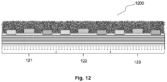
- Fig. 12 illustrates an EC 1200, falling under the claimed invention, having three first, second, and third transistors 121, 122 and 123 fabricated on the same layers.
- any number can be put on a given layer, e.g. 2, 3, 4, ..., millions or even billions in the case of some ICs.
- the subcomponents illustrated as transistors could instead be diodes, LEDs, resistors, capacitors, etc., depending on the EC.
- the BNNTs 111 as illustrated in Fig. 11 along with any coatings or compositing materials, may be placed across the multiple subcomponents to enhance transport of heat in the direction into or out of the page.
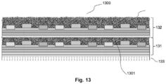
- Fig. 13 illustrates an EC 1300 falling under the claimed invention with two first and second layers 131 and 132 similar to the layer illustrated in Fig. 12 , forming a multilayer IC.
- a single heat sink 133 is included in this embodiment.
- the BNNT layer 1301 forms a back-side layer to the second layer 132, while being a top-side layer for the first layer 131.
- Interlayer connects and subcomponents such as capacitors are not illustrated, but as one of ordinary skill in the art should appreciate, a number of interconnects, sublayers, and subcomponents may make up the EC 1300.
- the BNNT bundles provide modified dielectric constants, in particular lower dielectric constants due to the porosity of the BNNTs, which for ECs and ICs operating with varying electrical flows will reduce the component heating in most applications.
- Fig. 14 illustrates an embodiment of an EC 1400 falling under the claimed invention with three first, second, and third primary layers 148, 149 and 1410.
- Each primary layer in this embodiment includes multiple first to fifth sublayers 142-146 for illustrative purposes, and multiple subcomponents 147.
- a single heat sink 141 is illustrated, though in practice there may be other heat sinks, such as top-side heat sinks.
- the BNNT layers illustrated in Fig. 14 as the fifth sublayers 146 provide thermal conductivity and low dielectric properties in a direction into and out of the drawing. The dielectric properties may be manipulated by controlling the level of alignment of the BNNTs going into the BNNT layers.
- Inter-layer and sublayer BNNT interconnects 1412 and first, second, and third layer and sublayer connections 1411, 1413, and 1414 provide thermal transport that can be either electrically insulating with associated dielectric properties, or electrically conductive or semiconductive.
- different sublayers may have different properties, e.g., one sublayer may be electrically insulating and another sublayer may be electrically conductive.
- Each of the inter-layer and sublayer BNNT interconnect 1412 and the first, second, and third layer and sublayer connections 1411, 1413, and 1414 may be, for example, a BNNT bundle cut to precisely fit the application.
- each BNNT bundle can be prepared as a string or yarn with the various compositing materials interspersed periodically along the BNNT bundle for connecting to the inter-layer connection points, and the BNNT string or yarn can be threaded through the interconnect locations.
- the selection of ceramic, metal, and/or polymer material utilized to composite or coat the BNNTs and/or portions thereof, may be used to control the properties of sublayers.
- portions of the BNNTs in a first sublayer may be composited or coated with a ceramic
- portions of the BNNTs in a second sublayer may be composited or coated with a polymer material. In this way the thermal connection to a given layer can be enhanced by optimizing the compositing or coating material for the thermal connection to the materials in the given sublayer or layer.
- Interlayer connects and subcomponents such as metal conductors, capacitors and interconnects for connecting the EC to other components are not illustrated, but as one of ordinary skill in the art of ICs and multilayer ICs should appreciate, a very diverse number of interconnects, sublayers and subcomponents may make up a multilayer IC.
- Diodes including light-emitting diodes, represent another category of ECs that may benefit through the incorporation of BNNTs.
- Fig. 15 illustrates a light emitting diode 1500 that includes the following layers and components: heat sink 151, baseplate 152, interface 153, solder 154, transition heat sink 155, attach layer 156, emitter or LED emitter 157, phosphor 158, resin-glue 159, lens 1510 and electrode 1511. These layers and components are meant to be illustrative of common light-emitting diodes, and embodiments may vary.
- BNNTs can be included in any layer that can be made of compositing materials compatible with being composited with BNNTs to include the heat sink 151, solder 154, resin-glue 159 and lens 1510.
- resin-glue 159 allows for lowering the critical junction temperature of the emitter or LED emitter 157.
- the BNNTs increase the porosity and thereby lower the dielectric value of the resin-glue 159, providing lower heat going into the attach layer 156 junction.
- the geometry of the BNNTs used for multilayer interconnects may vary greatly in cross sectional area and length.
- the BNNTs themselves are typically in the 1.5 to 6 nm diameter and their lengths can vary from 10s of nm to 100s of micrometers (microns). Consequently a great range of possibilities exists for assembling small to very large numbers of BNNTs to form the BNNT bundles, yarns and/or strings.
- Figs. 8 , 9 , 10 , 11 , 12 , 13 , and 14 show the BNNT bundles to be in-plane or mostly in-plane.
- Fig. 14 shows some BNNT bundles that are out-of-plane with reference to the three layers illustrated and their sublayers.
- the preferred heat transport is in the direction of the aligned BNNTs.
- the close contact of the BNNTs creates BNNT tube-to-tube or fiber-to-fiber contacts that also enhance the heat conductivity across the BNNT fibers. So while the primary heat path is along the length of the BNNTs, there is also enhanced heat removal across the BNNT fibers.
- careful management of the BNNT alignment enhances the heat management in the ECs far beyond just putting BNNTs into the bulk materials as proposed by Raman or just putting BNNTs out-of-plane in limited locations as proposed by Arik.
- BNNTs provide the designer and fabricator of ECs great flexibility in engineering effective heat transport and electrical properties into ECs.
- the BNNT layer transports heat from the hottest regions to cooler regions where the heat can be dissipated from the EC.
- Heat transport in ECs may be enhanced by BNNT tube contact with the top-side and bottom-side materials in addition to being composited into materials making up the layers and multilayer structures.
- the heat contact may be enhanced by the presence of compositing material in contact with the BNNTs and the EC subcomponents.
- the BNNTs may be uncoated or coated with thin amounts of epoxy, thermal grease, or other material infused by CVD, plasma, electron beam, ion beam processes, etc. Small particles of amorphous BN, h-BN, and boron may also be present. Clamps or glues may be used to assist in keeping the BNNTs in contact with the top-side, bottom-side, etc. components.
- the embodiments described herein range from nanometers to centimeters in a single figure, i.e. seven orders of magnitude in scale. Many of the beneficial effects generally occur due to the few nm diameter of the typical BNNT coming in close contact with the few nm to micrometer (micron) scale structures of the ECs and transporting the heat to heat sinks, plus the ability of high quality BNNTs to transport heat from BNNT to BNNT thereby greatly spreading and transporting the heat over much longer distances and much larger areas. BNNTs provide the designer and fabricator of ECs and ICs great flexibility in engineering effective heat transport into ECs.
- the BNNTs transport heat from the hottest regions to cooler regions where the heat can be dissipated.
- the BNNTs being electrical insulators provide minimal interference with the electrically conductive materials in the ECs while offering the designer a new tool for the introduction of porosity at the nm and micrometer (micron) scales to optimize the dielectric properties such as achieving low-k for lower electrical loss and consequently lower heating, while at the same time the BNNTs' strength provides structural enhancements valuable for high temperature operation and thermal cycling of the ECs.
- amorphous boron amorphous boron nitride (BN) and/or hexagonal-boron nitride (h-BN) (sometimes referred to as BN platelets).
- a purification step may be utilized to remove these particles to achieve enhanced thermal conductivity performance. In some cases these particles may contribute to the enhanced thermal conductivity.
- the ECs will also be more resilient to external forces by the addition of BNNT due to its exceptional strength.
- the BNNT based composites will better withstand large thermal variations, vibrations, accelerations, etc. thereby providing improved performance especially in extreme environments.
Claims (11)
- Composant électronique (1100 ; 1200) comprenant :une couche de matériau ayant une surface de contact, dans lequel la surface de contact inclut une source (112) et un drain (114) ; etune couche de groupe de nanotubes de nitrure de bore (BNNT) en contact avec la surface de contact,dans lequel la couche de groupe de BNNT comprend des BNNT (111) alignés de manière générale parallèlement à la surface de contact, de sorte que les BNNT (111) dans la couche de groupe de BNNT sont alignés de manière générale parallèlement à la surface de contact, etdans lequel au moins une partie des BNNT (111) dans la couche de groupe de BNNT pénètre dans la surface de contact, de sorte que la couche de groupe de BNNT est incrustée dans la surface de contact,caractérisé en ce que la couche de groupe de BNNT est en contact avec la source (112) et le drain (114).
- Composant électronique (1100 ; 1200 ; 1300 ; 1400) comprenant :une couche de matériau ayant une surface de contact, dans lequel la surface de contact inclut une source (112), un drain (114) et une grille (113) ; etune couche de groupe de nanotubes de nitrure de bore (BNNT) en contact avec la surface de contact,dans lequel la couche de groupe de BNNT est en contact avec la source (112), la grille (113), et le drain (114),caractérisé en ce que la couche de groupe de BNNT comprend des BNNT (111) alignés de manière générale parallèlement à la surface de contact,de sorte que les BNNT (111) dans la couche de groupe de BNNT sont alignés de manière générale parallèlement à la surface de contact, et en ce que l'au moins une partie des BNNT (111) dans la couche de groupe de BNNT pénètre dans la surface de contact, de sorte que la couche de groupe de BNNT est incrustée dans la surface de contact.
- Composant électronique (1100 ; 1200 ; 1300 ; 1400) selon la revendication 1 ou la revendication 2, dans lequel la couche de groupe de BNNT est formée en composite jusque dans la couche de matériau.
- Composant électronique (1100 ; 1200 ; 1300 ; 1400) selon la revendication 1 ou la revendication 2, dans lequel les BNNT (111) formant la couche de groupe de BNNT sont de manière générale parallèles les uns aux autres.
- Composant électronique (1100 ; 1200 ; 1300 ; 1400) selon la revendication 1 ou la revendication 2, dans lequel la couche de groupe de BNNT comprend :
au moins un élément parmi un tapis de BNNT (501) et un faisceau de BNNT ; ou au moins un matériau de formation de composite (703 ; 713 ; 723). - Composant électronique (1100 ; 1200 ; 1300 ; 1400) selon la revendication 1 ou la revendication 2, dans lequel la couche de groupe de BNNT comprend au moins un matériau de formation de composite (703 ; 713 ; 723) et l'au moins un matériau de formation de composite (703 ; 713 ; 723) est au moins un élément parmi une céramique, un métal, un polymère, une résine époxy, et une graisse thermique.
- Composant électronique (1100 ; 1200 ; 1300 ; 1400) selon la revendication 1 ou la revendication 2, dans lequel la couche de groupe de BNNT est :soumise à l'infusion d'une matériau de formation de composite (703 ; 713 ; 723) ;ou formée en composite avec un conducteur électrique ; oucomprimée jusque dans la couche de matériau.
- Composant électronique (1300 ; 1400) selon la revendication 2, dans lequel un premier côté de la couche de groupe de BNNT est en contact avec la surface de contact de la couche de matériau, la couche de matériau est une première couche de matériau, et le composant électronique (1300 ; 1400) comprend en outre une deuxième couche de matériau, sur un deuxième côté de la couche de groupe de BNNT.
- Composant électronique (1100 ; 1200 ; 1300 ; 1400) selon la revendication 2, dans lequel la couche de groupe de BNNT comprend une infusion spécifique d'un site, de sorte qu'un matériau de formation de composite (102, 103 ; 105, 106, 107) est infusé dans une partie de la couche de groupe de BNNT.
- Composant électronique (1100 ; 1200 ; 1300 ; 1400) selon la revendication 1 ou la revendication 2, dans lequel la couche de groupe de BNNT comprend une extrémité terminale, et l'extrémité terminale est exposée à l'environnement.
- Composant électronique (1100 ; 1200 ; 1300 ; 1400) selon la revendication 1 ou la revendication 2, dans lequel la couche de groupe de BNNT comprend une extrémité terminale, et l'extrémité terminale est incrustée dans un matériau de formation de composite (102, 103 ; 105, 107).
Applications Claiming Priority (5)
| Application Number | Priority Date | Filing Date | Title |
|---|---|---|---|
| US201462092906P | 2014-12-17 | 2014-12-17 | |
| US201562153155P | 2015-04-27 | 2015-04-27 | |
| US201562180353P | 2015-06-16 | 2015-06-16 | |
| US201562185329P | 2015-06-26 | 2015-06-26 | |
| PCT/US2015/066464 WO2016100715A1 (fr) | 2014-12-17 | 2015-12-17 | Composants électriques améliorés à nanotubes de nitrure de bore |
Publications (3)
| Publication Number | Publication Date |
|---|---|
| EP3233733A1 EP3233733A1 (fr) | 2017-10-25 |
| EP3233733A4 EP3233733A4 (fr) | 2018-11-21 |
| EP3233733B1 true EP3233733B1 (fr) | 2023-02-01 |
Family
ID=56127627
Family Applications (1)
| Application Number | Title | Priority Date | Filing Date |
|---|---|---|---|
| EP15871103.6A Active EP3233733B1 (fr) | 2014-12-17 | 2015-12-17 | Composants électroniques améliorés à nanotubes de nitrure de bore |
Country Status (5)
| Country | Link |
|---|---|
| US (2) | US10083890B2 (fr) |
| EP (1) | EP3233733B1 (fr) |
| KR (2) | KR20230048460A (fr) |
| CA (1) | CA2972769C (fr) |
| WO (1) | WO2016100715A1 (fr) |
Families Citing this family (13)
| Publication number | Priority date | Publication date | Assignee | Title |
|---|---|---|---|---|
| KR102515356B1 (ko) | 2014-11-01 | 2023-03-30 | 비엔엔티 엘엘씨 | Bnnt 합성을 위한 타겟 홀더, 다입사각 및 다영역 가열 |
| CA2985795C (fr) | 2015-05-13 | 2023-11-07 | Bnnt, Llc | Detecteur de neutrons a nanotubes de nitrure de bore |
| US10442691B2 (en) | 2015-05-21 | 2019-10-15 | Bnnt, Llc | Boron nitride nanotube synthesis via direct induction |
| US11362400B2 (en) * | 2016-02-02 | 2022-06-14 | Bnnt, Llc | Nano-porous BNNT composite with thermal switching for advanced batteries |
| JP7160825B2 (ja) * | 2016-11-29 | 2022-10-25 | ビイエヌエヌティ・エルエルシイ | クライオポンプ及び他の大容量構造用の窒化ホウ素ナノチューブ材料の形成方法 |
| US10686227B2 (en) * | 2016-12-01 | 2020-06-16 | The Regents Of The University Of California | High temperature Li-ion battery cells utilizing boron nitride aerogels and boron nitride nanotubes |
| WO2018148286A1 (fr) * | 2017-02-07 | 2018-08-16 | Bnnt, Llc | Amortissement des vibrations de nanotubes de nitrure de bore |
| DE102017217039A1 (de) | 2017-09-26 | 2019-03-28 | Robert Bosch Gmbh | Elektrochemische Festkörperzelle umfassend Bornitrid-Nanoröhrchen-Membran |
| CA3080219A1 (fr) * | 2017-10-27 | 2019-05-02 | National Research Council Of Canada | Substrats revetus de nanotubes de nitrure de bore destines au frittage de traces metalliques par une lumiere pulsee intense |
| US11332369B2 (en) * | 2018-03-22 | 2022-05-17 | BNNano, Inc. | Compositions and aggregates comprising boron nitride nanotube structures, and methods of making |
| EP4094100A2 (fr) * | 2020-01-21 | 2022-11-30 | Bnnt, Llc | Scintillateurs à nanotubes de nitrure de bore (bnnt) revêtus de cristaux |
| EP3878986A1 (fr) | 2020-03-12 | 2021-09-15 | Heraeus Deutschland GmbH & Co KG | Fil et ruban avec nanotubes de bornitrure pour contacts électriques |
| US20210325553A1 (en) * | 2020-04-17 | 2021-10-21 | The United States of America, as represnted by the Secratray of the Navy | MEMS Nanotube Based Thermal Neutron Detector |
Citations (3)
| Publication number | Priority date | Publication date | Assignee | Title |
|---|---|---|---|---|
| US20050006754A1 (en) * | 2003-07-07 | 2005-01-13 | Mehmet Arik | Electronic devices and methods for making same using nanotube regions to assist in thermal heat-sinking |
| US20080138577A1 (en) * | 2006-08-07 | 2008-06-12 | Daniel Peter Sheehan | Nano-fiber arrayed surfaces |
| US20120276666A1 (en) * | 2011-04-29 | 2012-11-01 | Hon Hai Precision Industry Co., Ltd. | Method for making light emitting diode |
Family Cites Families (49)
| Publication number | Priority date | Publication date | Assignee | Title |
|---|---|---|---|---|
| NL280732A (fr) | 1961-07-10 | |||
| GB1050932A (fr) | 1963-05-30 | |||
| US6893906B2 (en) | 1990-11-26 | 2005-05-17 | Semiconductor Energy Laboratory Co., Ltd. | Electro-optical device and driving method for the same |
| US5305612A (en) | 1992-07-06 | 1994-04-26 | Ebara Technologies Incorporated | Cryopump method and apparatus |
| US5820681A (en) | 1995-05-03 | 1998-10-13 | Chorus Corporation | Unibody crucible and effusion cell employing such a crucible |
| US6682677B2 (en) | 2000-11-03 | 2004-01-27 | Honeywell International Inc. | Spinning, processing, and applications of carbon nanotube filaments, ribbons, and yarns |
| GB0201600D0 (en) | 2002-01-24 | 2002-03-13 | Univ Cambridge Tech | Large- scale plasma synthesis of hollow nanostructures |
| US7582880B2 (en) | 2002-03-20 | 2009-09-01 | Neutron Sciences, Inc. | Neutron detector using lithiated glass-scintillating particle composite |
| US20060099135A1 (en) * | 2002-09-10 | 2006-05-11 | Yodh Arjun G | Carbon nanotubes: high solids dispersions and nematic gels thereof |
| US20050116336A1 (en) * | 2003-09-16 | 2005-06-02 | Koila, Inc. | Nano-composite materials for thermal management applications |
| US20050126766A1 (en) * | 2003-09-16 | 2005-06-16 | Koila,Inc. | Nanostructure augmentation of surfaces for enhanced thermal transfer with improved contact |
| DE102004001340A1 (de) * | 2004-01-08 | 2005-08-04 | Infineon Technologies Ag | Verfahren zum Herstellen eines Nanoelement-Feldeffektransistors, Nanoelement-Feldeffekttransistor und Nanoelement-Anordnung |
| US7320224B2 (en) | 2004-01-21 | 2008-01-22 | Brooks Automation, Inc. | Method and apparatus for detecting and measuring state of fullness in cryopumps |
| US7384448B2 (en) | 2004-02-16 | 2008-06-10 | Climax Engineered Materials, Llc | Method and apparatus for producing nano-particles of silver |
| US20060057388A1 (en) * | 2004-09-10 | 2006-03-16 | Sungho Jin | Aligned and open-ended nanotube structure and method for making the same |
| CN103276486B (zh) * | 2004-11-09 | 2017-12-15 | 得克萨斯大学体系董事会 | 纳米纤维纱线、带和板的制造和应用 |
| US20060173397A1 (en) | 2004-11-23 | 2006-08-03 | Hosheng Tu | Ophthalmology implants and methods of manufacture |
| US20070004225A1 (en) | 2005-06-30 | 2007-01-04 | Donghui Lu | Low-temperature catalyzed formation of segmented nanowire of dielectric material |
| CN101506413A (zh) * | 2006-03-03 | 2009-08-12 | 伊利诺伊大学评议会 | 制造空间排列的纳米管和纳米管阵列的方法 |
| US7335890B2 (en) | 2006-06-22 | 2008-02-26 | General Electric Company | Method and apparatus for detecting atomic particles |
| US8020508B2 (en) | 2006-09-19 | 2011-09-20 | The Board Of Regents Of The University Of Oklahoma | Methods and apparatus for depositing nanoparticles on a substrate |
| JP2010510168A (ja) | 2006-11-22 | 2010-04-02 | ザ リージェンツ オブ ザ ユニバーシティ オブ カリフォルニア | 官能化窒化ホウ素ナノチューブ |
| US7786024B2 (en) * | 2006-11-29 | 2010-08-31 | Nanosys, Inc. | Selective processing of semiconductor nanowires by polarized visible radiation |
| US7956345B2 (en) * | 2007-01-24 | 2011-06-07 | Stmicroelectronics Asia Pacific Pte. Ltd. | CNT devices, low-temperature fabrication of CNT and CNT photo-resists |
| CN101627161B (zh) | 2007-03-05 | 2012-08-15 | 帝人株式会社 | 氮化硼类纤维纸及其制造方法 |
| US8206674B2 (en) | 2007-05-15 | 2012-06-26 | National Institute Of Aerospace Associates | Boron nitride nanotubes |
| FI20075482L (fi) * | 2007-06-25 | 2008-12-26 | Canatu Oy | Kuituverkostot sekä menetelmä ja laite kuituverkostojen jatkuvasti tai erinä tapahtuvaan tuotantoon |
| US7927525B2 (en) | 2007-08-24 | 2011-04-19 | Lizotte Todd E | Vacuum isostatic micro molding of micro/nano structures and micro transfer metal films into PTFE and PTFE compounds |
| US8575641B2 (en) * | 2011-08-11 | 2013-11-05 | Goldeneye, Inc | Solid state light sources based on thermally conductive luminescent elements containing interconnects |
| US8569848B2 (en) * | 2008-07-21 | 2013-10-29 | The Regents Of The University Of California | Nanotube phonon waveguide |
| US20100192535A1 (en) | 2009-02-04 | 2010-08-05 | Smith Michael W | Boron nitride nanotube fibrils and yarns |
| US8679300B2 (en) | 2009-02-04 | 2014-03-25 | Jefferson Science Associates, Llc | Integrated rig for the production of boron nitride nanotubes via the pressurized vapor-condenser method |
| US8309242B2 (en) | 2009-11-03 | 2012-11-13 | Nokia Corporation | Battery cell |
| CA2778433C (fr) | 2009-12-10 | 2014-07-08 | Novelis Inc. | Structure de confinement de metal fondu comprenant une ventilation de circulation traversante |
| US8652992B2 (en) | 2009-12-15 | 2014-02-18 | SDCmaterials, Inc. | Pinning and affixing nano-active material |
| WO2011119494A1 (fr) | 2010-03-22 | 2011-09-29 | The Regents Of The University Of California | Procédé et dispositif pour synthétiser des nanotubes de nitrure de bore et des nanoparticules associées |
| US8795899B2 (en) | 2010-08-19 | 2014-08-05 | Nanotek Instruments, Inc. | Lithium super-battery with a functionalized nano graphene cathode |
| US8673120B2 (en) | 2011-01-04 | 2014-03-18 | Jefferson Science Associates, Llc | Efficient boron nitride nanotube formation via combined laser-gas flow levitation |
| US9279894B2 (en) | 2011-02-09 | 2016-03-08 | Lawrence Livermore National Security, Llc | Systems and methods for neutron detection using scintillator nano-materials |
| CN102760804B (zh) * | 2011-04-29 | 2015-01-21 | 清华大学 | 发光二极管 |
| US20130144576A1 (en) | 2011-11-10 | 2013-06-06 | U.S.A. as represented by the Administrator of the National Aeronautics and Space Admimistration | Modeling of Laser Ablation and Plume Chemistry in a Boron Nitride Nanotube Production Rig |
| US9825154B2 (en) | 2011-11-28 | 2017-11-21 | Michigan Technological University | Room temperature tunneling switches and methods of making and using the same |
| US20140080954A1 (en) | 2012-09-19 | 2014-03-20 | Chandrashekar Raman | Methods for making thermally conductve compositions containing boron nitride |
| US20140364529A1 (en) | 2013-04-03 | 2014-12-11 | U.S.A. As Represented By The Administrator Of The National Aeronautics And Space Administration | Sequential/simultaneous multi-metalized nanocomposites (s2m2n) |
| WO2014169382A1 (fr) | 2013-04-18 | 2014-10-23 | National Research Council Of Canada | Nanotubes de nitrure de bore et leur procédé de production |
| US10458049B2 (en) | 2013-07-30 | 2019-10-29 | University Of New Hampshire | Continuous boron nitride nanotube yarns and methods of production |
| US10343908B2 (en) | 2013-11-01 | 2019-07-09 | Bnnt, Llc | Induction-coupled plasma synthesis of boron nitrade nanotubes |
| KR101771872B1 (ko) | 2014-04-24 | 2017-08-25 | 비엔엔티 엘엘씨 | 연속 질화붕소 나노튜브 섬유 |
| US20160144401A1 (en) * | 2014-06-06 | 2016-05-26 | The University Of Massachusetts | Method for orienting one-dimensional objects and articles obtained therefrom |
-
2015
- 2015-12-17 WO PCT/US2015/066464 patent/WO2016100715A1/fr active Application Filing
- 2015-12-17 EP EP15871103.6A patent/EP3233733B1/fr active Active
- 2015-12-17 KR KR1020237010930A patent/KR20230048460A/ko active IP Right Grant
- 2015-12-17 KR KR1020177019472A patent/KR102517816B1/ko active IP Right Grant
- 2015-12-17 US US15/540,539 patent/US10083890B2/en active Active
- 2015-12-17 CA CA2972769A patent/CA2972769C/fr active Active
-
2018
- 2018-08-22 US US16/109,391 patent/US10573576B2/en active Active
Patent Citations (3)
| Publication number | Priority date | Publication date | Assignee | Title |
|---|---|---|---|---|
| US20050006754A1 (en) * | 2003-07-07 | 2005-01-13 | Mehmet Arik | Electronic devices and methods for making same using nanotube regions to assist in thermal heat-sinking |
| US20080138577A1 (en) * | 2006-08-07 | 2008-06-12 | Daniel Peter Sheehan | Nano-fiber arrayed surfaces |
| US20120276666A1 (en) * | 2011-04-29 | 2012-11-01 | Hon Hai Precision Industry Co., Ltd. | Method for making light emitting diode |
Also Published As
| Publication number | Publication date |
|---|---|
| EP3233733A1 (fr) | 2017-10-25 |
| US10083890B2 (en) | 2018-09-25 |
| KR20170097692A (ko) | 2017-08-28 |
| US20170352606A1 (en) | 2017-12-07 |
| CA2972769A1 (fr) | 2016-06-23 |
| KR20230048460A (ko) | 2023-04-11 |
| KR102517816B1 (ko) | 2023-04-04 |
| EP3233733A4 (fr) | 2018-11-21 |
| WO2016100715A1 (fr) | 2016-06-23 |
| US10573576B2 (en) | 2020-02-25 |
| US20190198418A1 (en) | 2019-06-27 |
| CA2972769C (fr) | 2023-01-03 |
Similar Documents
| Publication | Publication Date | Title |
|---|---|---|
| US10573576B2 (en) | Boron nitride nanotube enhanced electrical components | |
| KR102570247B1 (ko) | 카본나노튜브 복합재 및 카본나노튜브 복합재의 제조방법 | |
| Li et al. | Carbon nanomaterials: The ideal interconnect technology for next-generation ICs | |
| KR100904043B1 (ko) | 금속기 탄소섬유 복합재료 및 그 제조방법 | |
| EP2279522B1 (fr) | Dispositifs de chauffage à nanofil et procédé d'utilisation | |
| JP5628312B2 (ja) | ナノチューブの熱インターフェース構造 | |
| KR101007621B1 (ko) | 미크론 사이즈 및 나노 사이즈의 탄소섬유를 모두 함유하는금속기 복합재료 | |
| Zhang et al. | Vertically aligned graphene film/epoxy composites as heat dissipating materials | |
| JP5356972B2 (ja) | 放熱用部品及びその製造方法、半導体パッケージ | |
| WO2013046291A1 (fr) | Matériau dissipateur thermique et son procédé de production et dispositif électronique et son procédé de production | |
| EP2546871A1 (fr) | Structure de dissipation de chaleur, et procédé de fabrication de celle-ci | |
| JP5441486B2 (ja) | 熱界面材料の製造方法 | |
| JP2013115094A (ja) | 放熱材料及びその製造方法 | |
| KR20130061514A (ko) | 그래핀과 폴리머의 복합체 및 그 제조방법 | |
| DE102012018387A1 (de) | Textiler thermoelektrischer Generator | |
| JP2007281070A (ja) | 熱電変換素子およびその製造方法 | |
| WO2015097878A1 (fr) | Structure du type feuille, instrument électronique l'utilisant, procédé de fabrication de structure du type feuille et procédé de fabrication d'instrument électronique | |
| JP2016092334A (ja) | 放熱シート、放熱シートの製造方法、及び電子装置の製造方法 | |
| US20150145162A1 (en) | Method for making nanostructures | |
| Luo et al. | High‐Performance, Multifunctional, and Designable Carbon Fiber Felt Skeleton Epoxy Resin Composites EP/CF‐(CNT/AgBNs) x for Thermal Conductivity and Electromagnetic Interference Shielding | |
| JP6354235B2 (ja) | 電子機器とその組み立て方法、及びシート状構造体とその製造方法 | |
| KR20200080961A (ko) | 절연 방열 나노와이어, 이의 제조방법 및 이를 포함하는 복합체 | |
| WO2008050906A1 (fr) | Matériau composite et son procédé de production | |
| US8808857B1 (en) | Carbon nanotube array interface material and methods | |
| US20230303395A1 (en) | Carbon nanotube composite wire |
Legal Events
| Date | Code | Title | Description |
|---|---|---|---|
| STAA | Information on the status of an ep patent application or granted ep patent |
Free format text: STATUS: THE INTERNATIONAL PUBLICATION HAS BEEN MADE |
|
| PUAI | Public reference made under article 153(3) epc to a published international application that has entered the european phase |
Free format text: ORIGINAL CODE: 0009012 |
|
| STAA | Information on the status of an ep patent application or granted ep patent |
Free format text: STATUS: REQUEST FOR EXAMINATION WAS MADE |
|
| 17P | Request for examination filed |
Effective date: 20170713 |
|
| AK | Designated contracting states |
Kind code of ref document: A1 Designated state(s): AL AT BE BG CH CY CZ DE DK EE ES FI FR GB GR HR HU IE IS IT LI LT LU LV MC MK MT NL NO PL PT RO RS SE SI SK SM TR |
|
| AX | Request for extension of the european patent |
Extension state: BA ME |
|
| DAV | Request for validation of the european patent (deleted) | ||
| DAX | Request for extension of the european patent (deleted) | ||
| A4 | Supplementary search report drawn up and despatched |
Effective date: 20181022 |
|
| RIC1 | Information provided on ipc code assigned before grant |
Ipc: H01L 33/64 20100101ALI20181016BHEP Ipc: B82Y 30/00 20110101AFI20181016BHEP Ipc: C01B 21/064 20060101ALI20181016BHEP Ipc: H01L 23/373 20060101ALI20181016BHEP |
|
| STAA | Information on the status of an ep patent application or granted ep patent |
Free format text: STATUS: EXAMINATION IS IN PROGRESS |
|
| 17Q | First examination report despatched |
Effective date: 20200716 |
|
| STAA | Information on the status of an ep patent application or granted ep patent |
Free format text: STATUS: EXAMINATION IS IN PROGRESS |
|
| STAA | Information on the status of an ep patent application or granted ep patent |
Free format text: STATUS: EXAMINATION IS IN PROGRESS |
|
| REG | Reference to a national code |
Ref country code: DE Ref legal event code: R079 Ref document number: 602015082459 Country of ref document: DE Free format text: PREVIOUS MAIN CLASS: C01B0035140000 Ipc: B82Y0030000000 |
|
| RIC1 | Information provided on ipc code assigned before grant |
Ipc: H01L 33/64 20100101ALN20220531BHEP Ipc: H01L 23/373 20060101ALI20220531BHEP Ipc: C01B 21/064 20060101ALI20220531BHEP Ipc: B82Y 30/00 20110101AFI20220531BHEP |
|
| GRAP | Despatch of communication of intention to grant a patent |
Free format text: ORIGINAL CODE: EPIDOSNIGR1 |
|
| STAA | Information on the status of an ep patent application or granted ep patent |
Free format text: STATUS: GRANT OF PATENT IS INTENDED |
|
| INTG | Intention to grant announced |
Effective date: 20220708 |
|
| GRAS | Grant fee paid |
Free format text: ORIGINAL CODE: EPIDOSNIGR3 |
|
| GRAA | (expected) grant |
Free format text: ORIGINAL CODE: 0009210 |
|
| STAA | Information on the status of an ep patent application or granted ep patent |
Free format text: STATUS: THE PATENT HAS BEEN GRANTED |
|
| AK | Designated contracting states |
Kind code of ref document: B1 Designated state(s): AL AT BE BG CH CY CZ DE DK EE ES FI FR GB GR HR HU IE IS IT LI LT LU LV MC MK MT NL NO PL PT RO RS SE SI SK SM TR |
|
| REG | Reference to a national code |
Ref country code: GB Ref legal event code: FG4D |
|
| REG | Reference to a national code |
Ref country code: CH Ref legal event code: EP Ref country code: AT Ref legal event code: REF Ref document number: 1546904 Country of ref document: AT Kind code of ref document: T Effective date: 20230215 |
|
| REG | Reference to a national code |
Ref country code: DE Ref legal event code: R096 Ref document number: 602015082459 Country of ref document: DE |
|
| REG | Reference to a national code |
Ref country code: IE Ref legal event code: FG4D |
|
| REG | Reference to a national code |
Ref country code: LT Ref legal event code: MG9D |
|
| REG | Reference to a national code |
Ref country code: NL Ref legal event code: MP Effective date: 20230201 |
|
| P01 | Opt-out of the competence of the unified patent court (upc) registered |
Effective date: 20230515 |
|
| REG | Reference to a national code |
Ref country code: AT Ref legal event code: MK05 Ref document number: 1546904 Country of ref document: AT Kind code of ref document: T Effective date: 20230201 |
|
| PG25 | Lapsed in a contracting state [announced via postgrant information from national office to epo] |
Ref country code: RS Free format text: LAPSE BECAUSE OF FAILURE TO SUBMIT A TRANSLATION OF THE DESCRIPTION OR TO PAY THE FEE WITHIN THE PRESCRIBED TIME-LIMIT Effective date: 20230201 Ref country code: PT Free format text: LAPSE BECAUSE OF FAILURE TO SUBMIT A TRANSLATION OF THE DESCRIPTION OR TO PAY THE FEE WITHIN THE PRESCRIBED TIME-LIMIT Effective date: 20230601 Ref country code: NO Free format text: LAPSE BECAUSE OF FAILURE TO SUBMIT A TRANSLATION OF THE DESCRIPTION OR TO PAY THE FEE WITHIN THE PRESCRIBED TIME-LIMIT Effective date: 20230501 Ref country code: NL Free format text: LAPSE BECAUSE OF FAILURE TO SUBMIT A TRANSLATION OF THE DESCRIPTION OR TO PAY THE FEE WITHIN THE PRESCRIBED TIME-LIMIT Effective date: 20230201 Ref country code: LV Free format text: LAPSE BECAUSE OF FAILURE TO SUBMIT A TRANSLATION OF THE DESCRIPTION OR TO PAY THE FEE WITHIN THE PRESCRIBED TIME-LIMIT Effective date: 20230201 Ref country code: LT Free format text: LAPSE BECAUSE OF FAILURE TO SUBMIT A TRANSLATION OF THE DESCRIPTION OR TO PAY THE FEE WITHIN THE PRESCRIBED TIME-LIMIT Effective date: 20230201 Ref country code: HR Free format text: LAPSE BECAUSE OF FAILURE TO SUBMIT A TRANSLATION OF THE DESCRIPTION OR TO PAY THE FEE WITHIN THE PRESCRIBED TIME-LIMIT Effective date: 20230201 Ref country code: ES Free format text: LAPSE BECAUSE OF FAILURE TO SUBMIT A TRANSLATION OF THE DESCRIPTION OR TO PAY THE FEE WITHIN THE PRESCRIBED TIME-LIMIT Effective date: 20230201 Ref country code: AT Free format text: LAPSE BECAUSE OF FAILURE TO SUBMIT A TRANSLATION OF THE DESCRIPTION OR TO PAY THE FEE WITHIN THE PRESCRIBED TIME-LIMIT Effective date: 20230201 |
|
| PG25 | Lapsed in a contracting state [announced via postgrant information from national office to epo] |
Ref country code: SE Free format text: LAPSE BECAUSE OF FAILURE TO SUBMIT A TRANSLATION OF THE DESCRIPTION OR TO PAY THE FEE WITHIN THE PRESCRIBED TIME-LIMIT Effective date: 20230201 Ref country code: PL Free format text: LAPSE BECAUSE OF FAILURE TO SUBMIT A TRANSLATION OF THE DESCRIPTION OR TO PAY THE FEE WITHIN THE PRESCRIBED TIME-LIMIT Effective date: 20230201 Ref country code: IS Free format text: LAPSE BECAUSE OF FAILURE TO SUBMIT A TRANSLATION OF THE DESCRIPTION OR TO PAY THE FEE WITHIN THE PRESCRIBED TIME-LIMIT Effective date: 20230601 Ref country code: GR Free format text: LAPSE BECAUSE OF FAILURE TO SUBMIT A TRANSLATION OF THE DESCRIPTION OR TO PAY THE FEE WITHIN THE PRESCRIBED TIME-LIMIT Effective date: 20230502 Ref country code: FI Free format text: LAPSE BECAUSE OF FAILURE TO SUBMIT A TRANSLATION OF THE DESCRIPTION OR TO PAY THE FEE WITHIN THE PRESCRIBED TIME-LIMIT Effective date: 20230201 |
|
| PG25 | Lapsed in a contracting state [announced via postgrant information from national office to epo] |
Ref country code: SM Free format text: LAPSE BECAUSE OF FAILURE TO SUBMIT A TRANSLATION OF THE DESCRIPTION OR TO PAY THE FEE WITHIN THE PRESCRIBED TIME-LIMIT Effective date: 20230201 Ref country code: RO Free format text: LAPSE BECAUSE OF FAILURE TO SUBMIT A TRANSLATION OF THE DESCRIPTION OR TO PAY THE FEE WITHIN THE PRESCRIBED TIME-LIMIT Effective date: 20230201 Ref country code: EE Free format text: LAPSE BECAUSE OF FAILURE TO SUBMIT A TRANSLATION OF THE DESCRIPTION OR TO PAY THE FEE WITHIN THE PRESCRIBED TIME-LIMIT Effective date: 20230201 Ref country code: DK Free format text: LAPSE BECAUSE OF FAILURE TO SUBMIT A TRANSLATION OF THE DESCRIPTION OR TO PAY THE FEE WITHIN THE PRESCRIBED TIME-LIMIT Effective date: 20230201 Ref country code: CZ Free format text: LAPSE BECAUSE OF FAILURE TO SUBMIT A TRANSLATION OF THE DESCRIPTION OR TO PAY THE FEE WITHIN THE PRESCRIBED TIME-LIMIT Effective date: 20230201 |
|
| REG | Reference to a national code |
Ref country code: DE Ref legal event code: R097 Ref document number: 602015082459 Country of ref document: DE |
|
| PG25 | Lapsed in a contracting state [announced via postgrant information from national office to epo] |
Ref country code: SK Free format text: LAPSE BECAUSE OF FAILURE TO SUBMIT A TRANSLATION OF THE DESCRIPTION OR TO PAY THE FEE WITHIN THE PRESCRIBED TIME-LIMIT Effective date: 20230201 |
|
| PLBE | No opposition filed within time limit |
Free format text: ORIGINAL CODE: 0009261 |
|
| STAA | Information on the status of an ep patent application or granted ep patent |
Free format text: STATUS: NO OPPOSITION FILED WITHIN TIME LIMIT |
|
| 26N | No opposition filed |
Effective date: 20231103 |
|
| PG25 | Lapsed in a contracting state [announced via postgrant information from national office to epo] |
Ref country code: SI Free format text: LAPSE BECAUSE OF FAILURE TO SUBMIT A TRANSLATION OF THE DESCRIPTION OR TO PAY THE FEE WITHIN THE PRESCRIBED TIME-LIMIT Effective date: 20230201 |