EP3232181B1 - Information processing device, information acquisition system, information processing method, image information acquisition method, and program - Google Patents
Information processing device, information acquisition system, information processing method, image information acquisition method, and program Download PDFInfo
- Publication number
- EP3232181B1 EP3232181B1 EP15866785.7A EP15866785A EP3232181B1 EP 3232181 B1 EP3232181 B1 EP 3232181B1 EP 15866785 A EP15866785 A EP 15866785A EP 3232181 B1 EP3232181 B1 EP 3232181B1
- Authority
- EP
- European Patent Office
- Prior art keywords
- image
- measurement subject
- fluorescence
- luminance value
- unit
- Prior art date
- Legal status (The legal status is an assumption and is not a legal conclusion. Google has not performed a legal analysis and makes no representation as to the accuracy of the status listed.)
- Active
Links
- 238000000034 method Methods 0.000 title claims description 92
- 230000010365 information processing Effects 0.000 title claims description 78
- 238000003672 processing method Methods 0.000 title claims description 16
- 238000005259 measurement Methods 0.000 claims description 142
- 238000002073 fluorescence micrograph Methods 0.000 claims description 133
- 238000003384 imaging method Methods 0.000 claims description 103
- 238000012545 processing Methods 0.000 claims description 74
- 239000013307 optical fiber Substances 0.000 claims description 70
- 239000000835 fiber Substances 0.000 claims description 66
- 230000003287 optical effect Effects 0.000 claims description 62
- 230000005284 excitation Effects 0.000 claims description 45
- 230000008859 change Effects 0.000 claims description 32
- 238000004590 computer program Methods 0.000 claims description 8
- 238000010586 diagram Methods 0.000 description 58
- 230000008569 process Effects 0.000 description 52
- 238000004891 communication Methods 0.000 description 22
- 239000004065 semiconductor Substances 0.000 description 15
- 230000006870 function Effects 0.000 description 14
- 210000004027 cell Anatomy 0.000 description 12
- 210000000056 organ Anatomy 0.000 description 11
- 238000005516 engineering process Methods 0.000 description 10
- 230000007246 mechanism Effects 0.000 description 10
- 230000005684 electric field Effects 0.000 description 9
- 230000000694 effects Effects 0.000 description 8
- 206010028980 Neoplasm Diseases 0.000 description 7
- 238000006243 chemical reaction Methods 0.000 description 7
- 238000001356 surgical procedure Methods 0.000 description 7
- 201000011510 cancer Diseases 0.000 description 6
- 238000005253 cladding Methods 0.000 description 6
- 239000000470 constituent Substances 0.000 description 6
- 239000000126 substance Substances 0.000 description 5
- 206010061218 Inflammation Diseases 0.000 description 4
- 238000001914 filtration Methods 0.000 description 4
- 230000004054 inflammatory process Effects 0.000 description 4
- 230000005236 sound signal Effects 0.000 description 4
- 238000002674 endoscopic surgery Methods 0.000 description 3
- 239000000284 extract Substances 0.000 description 3
- 238000001727 in vivo Methods 0.000 description 3
- 210000004185 liver Anatomy 0.000 description 3
- 230000004807 localization Effects 0.000 description 3
- 238000000386 microscopy Methods 0.000 description 3
- 239000011324 bead Substances 0.000 description 2
- 230000008878 coupling Effects 0.000 description 2
- 238000010168 coupling process Methods 0.000 description 2
- 238000005859 coupling reaction Methods 0.000 description 2
- 230000007423 decrease Effects 0.000 description 2
- 239000003814 drug Substances 0.000 description 2
- 238000002091 elastography Methods 0.000 description 2
- 239000007850 fluorescent dye Substances 0.000 description 2
- 239000011521 glass Substances 0.000 description 2
- 230000001151 other effect Effects 0.000 description 2
- 238000011165 process development Methods 0.000 description 2
- 230000000241 respiratory effect Effects 0.000 description 2
- 230000000007 visual effect Effects 0.000 description 2
- 206010016654 Fibrosis Diseases 0.000 description 1
- 208000005718 Stomach Neoplasms Diseases 0.000 description 1
- 238000010521 absorption reaction Methods 0.000 description 1
- 230000004075 alteration Effects 0.000 description 1
- 239000000090 biomarker Substances 0.000 description 1
- 230000015572 biosynthetic process Effects 0.000 description 1
- 238000012937 correction Methods 0.000 description 1
- 239000013078 crystal Substances 0.000 description 1
- 210000004748 cultured cell Anatomy 0.000 description 1
- 230000001419 dependent effect Effects 0.000 description 1
- 238000003745 diagnosis Methods 0.000 description 1
- 238000009792 diffusion process Methods 0.000 description 1
- 210000002919 epithelial cell Anatomy 0.000 description 1
- 230000004761 fibrosis Effects 0.000 description 1
- 238000000799 fluorescence microscopy Methods 0.000 description 1
- 206010017758 gastric cancer Diseases 0.000 description 1
- 238000002350 laparotomy Methods 0.000 description 1
- 239000004973 liquid crystal related substance Substances 0.000 description 1
- 201000007270 liver cancer Diseases 0.000 description 1
- 230000003908 liver function Effects 0.000 description 1
- 208000014018 liver neoplasm Diseases 0.000 description 1
- 210000004072 lung Anatomy 0.000 description 1
- 239000000463 material Substances 0.000 description 1
- 238000012986 modification Methods 0.000 description 1
- 230000004048 modification Effects 0.000 description 1
- 239000002105 nanoparticle Substances 0.000 description 1
- 210000004798 organs belonging to the digestive system Anatomy 0.000 description 1
- 230000002093 peripheral effect Effects 0.000 description 1
- 239000012466 permeate Substances 0.000 description 1
- 238000012805 post-processing Methods 0.000 description 1
- 238000011002 quantification Methods 0.000 description 1
- 238000011084 recovery Methods 0.000 description 1
- 238000012552 review Methods 0.000 description 1
- 229920006395 saturated elastomer Polymers 0.000 description 1
- 238000000926 separation method Methods 0.000 description 1
- 201000011549 stomach cancer Diseases 0.000 description 1
- 238000002834 transmittance Methods 0.000 description 1
Images


Classifications
-
- A—HUMAN NECESSITIES
- A61—MEDICAL OR VETERINARY SCIENCE; HYGIENE
- A61B—DIAGNOSIS; SURGERY; IDENTIFICATION
- A61B1/00—Instruments for performing medical examinations of the interior of cavities or tubes of the body by visual or photographical inspection, e.g. endoscopes; Illuminating arrangements therefor
- A61B1/00002—Operational features of endoscopes
- A61B1/00004—Operational features of endoscopes characterised by electronic signal processing
- A61B1/00006—Operational features of endoscopes characterised by electronic signal processing of control signals
-
- G—PHYSICS
- G01—MEASURING; TESTING
- G01N—INVESTIGATING OR ANALYSING MATERIALS BY DETERMINING THEIR CHEMICAL OR PHYSICAL PROPERTIES
- G01N21/00—Investigating or analysing materials by the use of optical means, i.e. using sub-millimetre waves, infrared, visible or ultraviolet light
- G01N21/62—Systems in which the material investigated is excited whereby it emits light or causes a change in wavelength of the incident light
- G01N21/63—Systems in which the material investigated is excited whereby it emits light or causes a change in wavelength of the incident light optically excited
- G01N21/64—Fluorescence; Phosphorescence
-
- A—HUMAN NECESSITIES
- A61—MEDICAL OR VETERINARY SCIENCE; HYGIENE
- A61B—DIAGNOSIS; SURGERY; IDENTIFICATION
- A61B1/00—Instruments for performing medical examinations of the interior of cavities or tubes of the body by visual or photographical inspection, e.g. endoscopes; Illuminating arrangements therefor
- A61B1/00002—Operational features of endoscopes
- A61B1/00004—Operational features of endoscopes characterised by electronic signal processing
- A61B1/00009—Operational features of endoscopes characterised by electronic signal processing of image signals during a use of endoscope
-
- A—HUMAN NECESSITIES
- A61—MEDICAL OR VETERINARY SCIENCE; HYGIENE
- A61B—DIAGNOSIS; SURGERY; IDENTIFICATION
- A61B1/00—Instruments for performing medical examinations of the interior of cavities or tubes of the body by visual or photographical inspection, e.g. endoscopes; Illuminating arrangements therefor
- A61B1/00163—Optical arrangements
- A61B1/00165—Optical arrangements with light-conductive means, e.g. fibre optics
-
- A—HUMAN NECESSITIES
- A61—MEDICAL OR VETERINARY SCIENCE; HYGIENE
- A61B—DIAGNOSIS; SURGERY; IDENTIFICATION
- A61B1/00—Instruments for performing medical examinations of the interior of cavities or tubes of the body by visual or photographical inspection, e.g. endoscopes; Illuminating arrangements therefor
- A61B1/00163—Optical arrangements
- A61B1/00172—Optical arrangements with means for scanning
-
- A—HUMAN NECESSITIES
- A61—MEDICAL OR VETERINARY SCIENCE; HYGIENE
- A61B—DIAGNOSIS; SURGERY; IDENTIFICATION
- A61B1/00—Instruments for performing medical examinations of the interior of cavities or tubes of the body by visual or photographical inspection, e.g. endoscopes; Illuminating arrangements therefor
- A61B1/04—Instruments for performing medical examinations of the interior of cavities or tubes of the body by visual or photographical inspection, e.g. endoscopes; Illuminating arrangements therefor combined with photographic or television appliances
- A61B1/043—Instruments for performing medical examinations of the interior of cavities or tubes of the body by visual or photographical inspection, e.g. endoscopes; Illuminating arrangements therefor combined with photographic or television appliances for fluorescence imaging
-
- A—HUMAN NECESSITIES
- A61—MEDICAL OR VETERINARY SCIENCE; HYGIENE
- A61B—DIAGNOSIS; SURGERY; IDENTIFICATION
- A61B5/00—Measuring for diagnostic purposes; Identification of persons
- A61B5/0059—Measuring for diagnostic purposes; Identification of persons using light, e.g. diagnosis by transillumination, diascopy, fluorescence
- A61B5/0071—Measuring for diagnostic purposes; Identification of persons using light, e.g. diagnosis by transillumination, diascopy, fluorescence by measuring fluorescence emission
-
- G—PHYSICS
- G01—MEASURING; TESTING
- G01J—MEASUREMENT OF INTENSITY, VELOCITY, SPECTRAL CONTENT, POLARISATION, PHASE OR PULSE CHARACTERISTICS OF INFRARED, VISIBLE OR ULTRAVIOLET LIGHT; COLORIMETRY; RADIATION PYROMETRY
- G01J1/00—Photometry, e.g. photographic exposure meter
- G01J1/58—Photometry, e.g. photographic exposure meter using luminescence generated by light
-
- G—PHYSICS
- G01—MEASURING; TESTING
- G01N—INVESTIGATING OR ANALYSING MATERIALS BY DETERMINING THEIR CHEMICAL OR PHYSICAL PROPERTIES
- G01N21/00—Investigating or analysing materials by the use of optical means, i.e. using sub-millimetre waves, infrared, visible or ultraviolet light
- G01N21/62—Systems in which the material investigated is excited whereby it emits light or causes a change in wavelength of the incident light
- G01N21/63—Systems in which the material investigated is excited whereby it emits light or causes a change in wavelength of the incident light optically excited
- G01N21/64—Fluorescence; Phosphorescence
- G01N21/645—Specially adapted constructive features of fluorimeters
- G01N21/6456—Spatial resolved fluorescence measurements; Imaging
- G01N21/6458—Fluorescence microscopy
-
- G—PHYSICS
- G02—OPTICS
- G02B—OPTICAL ELEMENTS, SYSTEMS OR APPARATUS
- G02B21/00—Microscopes
- G02B21/0004—Microscopes specially adapted for specific applications
- G02B21/002—Scanning microscopes
- G02B21/0024—Confocal scanning microscopes (CSOMs) or confocal "macroscopes"; Accessories which are not restricted to use with CSOMs, e.g. sample holders
- G02B21/0052—Optical details of the image generation
- G02B21/0076—Optical details of the image generation arrangements using fluorescence or luminescence
-
- G—PHYSICS
- G02—OPTICS
- G02B—OPTICAL ELEMENTS, SYSTEMS OR APPARATUS
- G02B21/00—Microscopes
- G02B21/06—Means for illuminating specimens
-
- G—PHYSICS
- G02—OPTICS
- G02B—OPTICAL ELEMENTS, SYSTEMS OR APPARATUS
- G02B21/00—Microscopes
- G02B21/16—Microscopes adapted for ultraviolet illumination ; Fluorescence microscopes
-
- G—PHYSICS
- G02—OPTICS
- G02B—OPTICAL ELEMENTS, SYSTEMS OR APPARATUS
- G02B21/00—Microscopes
- G02B21/36—Microscopes arranged for photographic purposes or projection purposes or digital imaging or video purposes including associated control and data processing arrangements
-
- G—PHYSICS
- G06—COMPUTING; CALCULATING OR COUNTING
- G06T—IMAGE DATA PROCESSING OR GENERATION, IN GENERAL
- G06T7/00—Image analysis
- G06T7/50—Depth or shape recovery
- G06T7/55—Depth or shape recovery from multiple images
- G06T7/571—Depth or shape recovery from multiple images from focus
-
- G—PHYSICS
- G06—COMPUTING; CALCULATING OR COUNTING
- G06T—IMAGE DATA PROCESSING OR GENERATION, IN GENERAL
- G06T2207/00—Indexing scheme for image analysis or image enhancement
- G06T2207/10—Image acquisition modality
- G06T2207/10056—Microscopic image
-
- G—PHYSICS
- G06—COMPUTING; CALCULATING OR COUNTING
- G06T—IMAGE DATA PROCESSING OR GENERATION, IN GENERAL
- G06T2207/00—Indexing scheme for image analysis or image enhancement
- G06T2207/10—Image acquisition modality
- G06T2207/10068—Endoscopic image
-
- G—PHYSICS
- G06—COMPUTING; CALCULATING OR COUNTING
- G06T—IMAGE DATA PROCESSING OR GENERATION, IN GENERAL
- G06T2207/00—Indexing scheme for image analysis or image enhancement
- G06T2207/30—Subject of image; Context of image processing
- G06T2207/30004—Biomedical image processing
Definitions
- the present disclosure relates to an information processing device, an image acquisition system, an information processing method, an image information acquisition method, and a program.
- a laser confocal microscope disclosed below in Patent Literature 1 has been proposed as a laser confocal microscope (a microendoscope) which uses an image guide fiber composed of a plurality of optical fiber element wires.
- a microendoscope system proposed in Patent Literature 1 transmits fluorescence generated by exciting an observation target with one photon through an image guide fiber and enables the generated fluorescence to be observed.
- Non-Patent Literature 1 discloses a method for specifying a position of a surface or a position of a focus of an observation target by applying an image recognition technology to a fluorescence image obtained using a field-of-view (FOV) type fluorescence microscope.
- FOV field-of-view
- Patent Literature 1 JP 2007-530197T
- Non-Patent Literature 1 is a technology of applying an image recognition process to a fluorescence image obtained using a specific fluorescence microscope.
- the present disclosure takes the above circumstances into consideration and proposes an information processing device, an image acquisition system, an information processing method, an image information acquisition method, and a program which enable a position of a surface of a measurement subject to be more simply specified with respect to an arbitrary fluorescence image.
- an information processing device According to the present disclosure, there is provided an information processing device according to claim 1.
- a thickness position corresponding to a fluorescence image that gives a maximum representative luminance value is set as a position corresponding to a surface of the measurement subject.
- a position of a surface of a measurement subject can be more simply specified with respect to an arbitrary fluorescence image.
- endoscope technologies have developed in recent years, surgical operations or intraoperative diagnoses have been conducted under endoscopes.
- a predetermined fluorescent dye is injected into an organ to be noted, and then a fluorescence image of the organ is observed using a fluorescence microscope connected to an endoscope.
- a measurement subject is fluorescent beads having a uniform diameter that is uniform and smaller than a focal depth
- a substance having a variable shape and a variety of thicknesses, like cells or the like is a measurement subject, it is not possible to specify a position of a surface thereof unless a three-dimensional structure of the measurement subject can be imagined, and thus specification of a position of a surface of a measurement subject depends on user proficiency. For this reason, a method in which a position of a surface of a measurement subject can be simply specified in a fluorescence image without relying on user proficiency has been desired.
- Non-Patent Literature 1 Applying the image recognition technology as described in Non-Patent Literature 1 is considered in order to, for example, specify a position of a surface of a measurement subject in a fluorescence image.
- the technology of Non-Patent Literature 1 is a technology applicable to a fluorescence image obtained using a specific fluorescence microscope, and using the technology entails difficulty.
- use of an auto-focus technology for detecting a position of slide glass is also considered, however, the technology is not applied under an environment in which no slide glass is used as in in-vivo somatoscopy.
- the inventor focused on using some kind of information that can be obtained from a fluorescence image to specify a position of a surface regardless of the use of a fluorescence microscope or a fluorescence excitement process.
- One kind of information considered as the information is an average luminance value of fluorescence images.
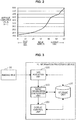
- FIG. 1 is an illustrative diagram for describing fluorescence images
- FIG. 2 is a graph diagram for describing the fluorescence images.
- fluorescence images brightness of bright spots generally brightens as the fluorescence images are observed on a side closer to a surface, and brightness of the bright spots darkens as the fluorescence images are observed on a side farther from the surface since a thickness that the fluorescence should permeate is increased, as schematically shown in FIG. 1 .
- fluorescence images tend to be bright overall at observation positions at which the fluorescence images are out of focus.
- the number of bright spots differs depending on observation positions of a measurement subject in a thickness direction (a depth direction) as schematically shown in FIG. 1 .
- FIG. 2 is a diagram in which a change in average luminance values of the fluorescence images when fluorescence that is generated by a certain cell is observed from a deep part side of the cell to a surface side with an interval of 5 ⁇ m is plotted.
- the horizontal axis represents numbers (image numbers) associated with the fluorescence images sequentially captured from the deep part side
- the vertical axis represents the average luminance values.
- the present inventor has decided to focus on a distribution of luminance values itself, rather than an average luminance value of fluorescence images, and has completed an information processing device and an image acquisition system according to an embodiment of the present disclosure to be described in detail below.
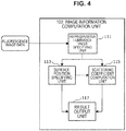
- FIG. 3 is a block diagram showing an example of a configuration of the information processing device according to the present embodiment
- FIG. 4 is a block diagram showing an example of a configuration of an image information computation unit provided in the information processing device according to the present embodiment
- FIGS. 5 to 9 are illustrative diagrams for describing an image information computation process according to the present embodiment.
- the information processing device 10 is a device which acquires a fluorescence image of a measurement subject captured by an imaging unit 20, uses the fluorescence image, and computes image information relevant to the fluorescence image including at least a position of a surface of the measurement subject.
- the information processing device 10 may be an information processing device such as any of a variety of computers and servers provided outside the imaging unit 20, or may be an arithmetic operation chip constituted by a central processing unit (CPU), a read only memory (ROM), a random access memory (RAM), and the like installed in the imaging unit 20.
- CPU central processing unit
- ROM read only memory
- RAM random access memory
- a measurement subject is not particularly limited as long as it is a substance that emits fluorescence, and the measurement subject may be an inanimate object such as a fluorescence bead or an animate object such as any of a variety of kinds of cells.
- fluorescence emitted from a measurement subject may be emitted by the measurement subject itself, or may be emitted by any of a variety of fluorescent dyes added to the measurement subject.
- an excitation process of such fluorescence and it may be fluorescence emitted from a fluorescent substance excited in a one-photon process, or may be fluorescence emitted from a fluorescence substance excited in a multiple-photon processes, for example, a two-photon process.
- the imaging unit 20 that captures such a fluorescence image is a unit which radiates excitation light having a predetermined wavelength toward a measurement subject, detects fluorescence generated from the measurement subject, and thereby generates image data regarding the generated fluorescence.
- Any device such as one of a variety of kinds of fluorescence microscopes can be used as the imaging unit 20 as long as the device can capture fluorescence images while changing a position of a measurement subject in the thickness direction.
- the information processing device 10 mainly has a data acquisition unit 101, an image information computation unit 103, a display control unit 105, and a storage unit 107 as illustrated in FIG. 3 .
- the data acquisition unit 101 is realized by, for example, a CPU, a ROM, a RAM, a communication device, and the like.
- the data acquisition unit 101 acquires image data of a plurality of fluorescence images generated by the imaging unit 20 in which the measurement subject has a different thickness direction from the imaging unit 20.
- the image data of the plurality of fluorescence images acquired by the data acquisition unit 101 is transmitted to the image information computation unit 103 to be described below.
- the data acquisition unit 101 may associate the acquired image data of the plurality of fluorescence images with time information regarding a date, time, and the like on which the image data is acquired and store the associated data in the storage unit 107 to be described below as history information.
- the image information computation unit 103 is realized by, for example, a CPU, a ROM, a RAM, and the like.
- the image information computation unit 103 computes image information including at least information regarding a position corresponding to a surface of the measurement subject using the plurality of fluorescence images transmitted from the data acquisition unit 101, in which the measurement subject has a different thickness direction.
- the image information computation unit 103 may also compute information regarding a scattering coefficient of the measurement subject as image information.
- the image information computation unit 103 outputs information regarding the computed image information to the display control unit 105.
- the image information regarding the fluorescence images of the measurement subject S is output to a display unit (not illustrated) provided in the information processing device 10 or any of various computers that can communicate with the information processing device 10.
- the image information computation unit 103 may output the obtained image information to any of a variety of recording media, computers, or the like, or to a paper medium using an output device such as a printer.
- the image information computation unit 103 may associate the image information regarding the fluorescence images of the measurement subject S with time information regarding a date, time, and the like at which the information was computed and store the associated data in the storage unit 107 or the like as history information.
- the display control unit 105 is realized by, for example, a CPU, a ROM, a RAM, an output device, and the like.
- the display control unit 105 performs display control to display a position of a surface of the measurement subject S or various processing results including the image information regarding the scattering coefficient of the measurement subject S or the like transmitted from the image information computation unit 103 on an output device such as a display of the information processing device 10 and an output device provided outside of the information processing device 10. Accordingly, a user of the information processing device 10 can immediately ascertain the various processing results with regard to the measurement subject S.
- the storage unit 107 is realized by, for example, a RAM of the information processing device 10 according to the present embodiment, a storage device, or the like.
- the storage unit 107 appropriately records various parameters or process developments that need to be saved by the information processing device 10 according to the present embodiment to perform any process, or various databases, programs, and the like.
- the storage unit 107 enables the data acquisition unit 101, the image information computation unit 103, the display control unit 105, and the like to freely perform data read and write processes.
- the image information computation unit 103 has, for example, a representative luminance value specifying unit 111, a surface position specifying unit 113, a scattering coefficient computation unit 115, and a result output unit 117 as illustrated in FIG. 4 .
- the representative luminance value specifying unit 111 is realized by, for example, a CPU, a ROM, a RAM, and the like.
- the representative luminance value specifying unit 111 executes, on the basis of the plurality of fluorescence images that were captured d while the position of the measurement subject S is changed in the thickness direction, a process (a sorting process) of sequentially rearranging luminance values constituting the plurality of fluorescence images from the highest luminance value for each of the fluorescence images corresponding to thickness positions thereof. Thereafter, the representative luminance value specifying unit 111 extracts a luminance value ranked at a predetermined position from the highest luminance value and sets the extracted luminance value as a representative luminance value of a fluorescence image at a thickness position to be noted.
- FIG. 5 shows results of a sorting process for luminance values performed using fluorescence images obtained by imaging fluorescence from eGFP generated from the measurement subject S (specifically, an eGFP-RFP expression cancer tissue cell created in an individual mouse: MKN 45 (a human gastric cancer epithelial cell)) while changing fluorescence by 5 ⁇ m in a depth direction.
- the horizontal axis represents numbers (image numbers: #1 to #60) linked to fluorescence images that are sequentially captured from the depth side, and a higher number denotes that the florescence image is approaching a surface side.
- the vertical axis represents luminance values.
- a fluorescence image that is the brightest and in focus is considered to be a fluorescence image for a surface of the measurement subject S.
- the fluorescence images have a substantially equal probability of having bright spots, the same bright spots can be regarded as being observed when luminance values of all pixels of the fluorescence images are sequentially sorted from the highest luminance value.
- FIG. 5 if a curve exponentially changes when a change in the luminance values in accordance with a change in a thickness position is plotted, the above-described precondition can be determined to be substantially satisfied.
- a position of a surface of the measurement subject S can be decided.
- the change in the luminance values is not even, but there are several peaks in the number #1 to the number #30.
- the reason for this is considered to be that electric noise caused by a laser, an image sensor, or the like that is used to generate the fluorescence images has been superimposed.
- luminance values are saturated from the number #35.
- the representative luminance value specifying unit 111 can specify the position of the surface of the measurement subject S to be noted by dealing with the luminance values ranked in the top 1% (i.e., the luminance values on the plot of "99%" in FIG. 5 ) among the plots shown in FIG. 5 as representative luminance values.
- a rank from the top position at which luminance values to be noted are positioned may be appropriately selected in accordance with a density of bright spots of a fluorescence image to be noted, however, for example, a rank in the range of the top 0.5% to 5% of the number of all pixels constituting one fluorescence image with reference to a highest luminance value is preferable.
- a case of a rank in the top 0.5% or less is not preferable because there is a possibility of various kinds of electric noise being superimposed on the luminance values like the plot of "Maximum" in FIG. 5 .
- a case of a rank exceeding the top 5% is not preferable because there is a possibility of luminance values increasing monotonously, like the plot of "90%" in FIG. 5 .
- the representative luminance value specifying unit 111 extracts a luminance value ranked at a predetermined position from the highest luminance value of each of fluorescence images as a representative luminance value.
- the representative luminance value specifying unit 111 outputs information of the representative luminance value extracted as described above to the surface position specifying unit 113 and the scattering coefficient computation unit 115 to be described below.
- the surface position specifying unit 113 is realized by, for example, a CPU, a ROM, a RAM, and the like.
- the surface position specifying unit 113 specifies a position corresponding to a surface of the measurement subject S on the basis of a representative luminance value of each fluorescence image extracted by the representative luminance value specifying unit 111. Specifically, the surface position specifying unit 113 sets a thickness position corresponding to a fluorescence image that gives a maximum representative luminance value among the representative luminance values of the respective fluorescence images as a position corresponding to the surface of the measurement subject S to be noted.
- the surface position specifying unit 113 outputs information regarding the position of the surface of the measurement subject S specified as described above to the scattering coefficient computation unit 115 and the result output unit 117 to be described below.
- the scattering coefficient computation unit 115 is realized by, for example, a CPU, a ROM, a RAM, and the like.
- the scattering coefficient computation unit 115 uses the representative luminance values of the respective fluorescence images and computes a scattering coefficient of the measurement subject from a degree of change in the representative luminance values in the thickness direction.
- luminance values at the ranks extracted as the representative luminance values exponentially change in accordance with a change in the position in the thickness direction.
- a scattering coefficient of the measurement subject S can be obtained from the degree of change.
- the scattering coefficient computation unit 115 computes a scattering coefficient using representative luminance values at three thickness positions having equal intervals on the basis of representative luminance values of fluorescence images corresponding to deeper parts than the position corresponding to the surface of the measurement subject S.
- a scattering coefficient computation process by the scattering coefficient computation unit 115 will be described in detail below with reference to FIG. 6 .
- BG a background luminance value
- the two following formulas 101 and 103 are established from a definition of the scattering coefficient R S .
- N is a known parameter decided in accordance with a fluorescence microscope used when the fluorescence images are captured
- dx is a known parameter set when the three representative luminance values are extracted
- a 1 to A 3 are the representative luminance values that can be obtained from the fluorescence images.
- FIGS. 7 to 9 show scattering coefficients R S of the measurement subject S computed with the formula 105 using fluorescence images captured using a two-photon fluorescence microscope. Note that the fluorescence images are the same as those used in generating FIG. 5 .
- FIG. 7 shows computation results of the scattering coefficients R S when dx is set to 10 ⁇ m
- FIG. 8 shows computation results of the scattering coefficients R S when dx is set to 25 ⁇ m
- FIG. 9 shows computation results of the scattering coefficients R S when dx is set to 35 ⁇ m.
- the scattering coefficient computation unit 115 sets a least uneven value at the position at which the luminance values sharply change among the scattering coefficients R S computed on the basis of the formula 105 as the scattering coefficient R S of the measurement subject S to be noted.
- the scattering coefficient computation unit 115 computes the scattering coefficient R S of the measurement subject S to be noted to be 5 (1/mm).
- the scattering coefficient computation unit 115 outputs information regarding the scattering coefficient R S of the measurement subject S computed as described above to the result output unit 117 to be described below.
- the result output unit 117 is realized by, for example, a CPU, a ROM, a RAM, an output device, a communication device, and the like.
- the result output unit 117 outputs information regarding the position of the surface of the measurement subject S specified by the surface position specifying unit 113 and information regarding the scattering coefficient R S of the measurement subject S computed by the scattering coefficient computation unit 115.
- the respective constituent elements may be configured using universal members and circuits, or may be configured using hardware specialized for the functions of the constituent elements.
- all of the functions of the constituent elements may be fulfilled by a CPU and the like.
- a configuration to be used can be appropriately changed in accordance with a technical level of any occasion at which the present embodiment is implemented.
- a computer program for realizing each function of the information processing device according to the above-described present embodiment can be produced and installed in a personal computer and the like.
- a computer-readable recording medium on which the computer program is stored can also be provided.
- the recording medium is, for example, a magnetic disk, an optical disc, a magneto-optical disc, a flash memory, or the like.
- the computer program may be distributed through, for example, a network, without using a recording medium.
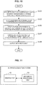
- FIG. 10 is a flowchart showing the example of the flow of the information processing method according to the present embodiment.
- the data acquisition unit 101 acquires a plurality of fluorescence images obtained from different thickness positions of the measurement subject S (Step S101).
- the data acquisition unit 101 outputs information regarding the plurality of acquired fluorescence images to the representative luminance value specifying unit 111 of the image information computation unit 103.
- the representative luminance value specifying unit 111 extracts representative luminance values from the plurality of respective fluorescence images using the fluorescence images output from the data acquisition unit 101 (Step S103). Then, the representative luminance value specifying unit 111 outputs information regarding the extracted representative luminance values to the surface position specifying unit 113 and the scattering coefficient computation unit 115.
- the surface position specifying unit 113 specifies a position at which a maximum representative luminance value is given as a position corresponding to a surface of the measurement subject S on the basis of the extracted representative luminance values (Step S105).
- the surface position specifying unit 113 outputs information regarding the specified position of the surface of the measurement subject S to the scattering coefficient computation unit 115 and the result output unit 117.
- the scattering coefficient computation unit 115 computes the scattering coefficient R S using the above-described formula 105 on the basis of the extracted representative luminance values (Step S107).
- the scattering coefficient computation unit 115 outputs information regarding the computed scattering coefficient R S to the result output unit 117.
- the result output unit 117 outputs the information regarding the position of the surface specified by the surface position specifying unit 113 and the information regarding the scattering coefficient computed by the scattering coefficient computation unit 115 to the outside (Step S109). Accordingly, a user of the information processing device 10 can ascertain image information regarding the fluorescence images of the measurement subject S.
- a surface position specifying method that does not depend on visual observation (in other words, that does not depend on a technique of a user) can be provided.
- the scattering coefficient R S of the measurement subject S can be computed. If the scattering coefficient R S of the measurement subject S is known, an intensity (power) necessary for acquiring a fluorescence image can be estimated, and thus important information for appropriately acquiring a fluorescence image can be obtained.
- the scattering coefficient R S can be computed if information can be acquired through observation from one side of the measurement subject S and the measurement subject S has a thickness of about dozens micrometers.
- information processing device 10 and the information processing method according to the present embodiment even information of an organ having high tissue porosity such as a lung can be acquired, and information can be acquired from a small tissue sample from an organ such as a liver.
- a doctor Ascertains a degree of inflammation or induration of the organ during the surgery and excises a sufficient area of the cancer tissue securing an extra margin if there is likely to be little induration, or leaves a large area of an organ tissue having a small margin if there is likely to be induration.
- the surgery is a laparotomy
- the doctor ascertains a degree of inflammation or induration of an organ of a patient by touching the organ with his or her hand or visually checking the organ.
- endoscopic surgeries have developed in recent years, minimally invasive endoscopic surgeries have been used most frequently.
- cancerous organs have scattering coefficients or absorption coefficients that are about 15% lower than those of normal tissues, and since the information processing device 10 and the information processing method according to the present embodiment can compute a scattering coefficient of a tissue from a fluorescence image, there is great merit in deciding a position to be excised and an intraoperative diagnosis of a cell in a gastroenterological surgery. In addition, the merit also contributes to the discovery of cancer cells in respiratory internal medicine, respiratory surgery, and urology. As described above, the information processing device 10 and the information processing method according to the present embodiment also provide useful information in the field of medicine.
- an image acquisition system that has an imaging function of imaging a fluorescence image of a measurement subject and the function of computing image information including a position of a surface and a scattering intensity of a measurement subject described in the first embodiment will be described in detail with reference to FIGS. 11 to 23 .
- fluorescence images are acquired using an image guide fiber constituted by a plurality of optical fiber element wires.
- the present inventor has separately reviewed a method for detecting fluorescence generated through a multi-photon excitation process in order to use such an image guide fiber.
- a guided wave of excitation light using an image guide fiber is in a single mode (more specifically, a zero-order mode) and, if an image guide fiber constituted by optical fiber element wires in a multi-mode is used as it is, a decrease or unevenness in luminance of the fluorescence occurs so as to make it impossible to acquire a fluorescence image using a multi-photon excitation process.
- optical fiber element wires constituting the image guide fiber are also considered to be set as optical fiber element wires in a single mode.
- reducing the difference in refractive index between the core and the cladding means an increase in diffusion of electric field intensity distribution toward the cladding.
- Resolution of the image guide fiber depends on arrangement intervals of the optical fiber element wires, and as the arrangement intervals of the optical fiber element wires is narrowed, the resolution obtained is increased.
- the optical fiber element wires in the single mode are used and intervals of the optical fiber element wires are widened, while another mechanism that scans the optical fiber to obtain the same degree of resolution as that of a normal image guide fiber is necessary, it is difficult to narrow a diameter of the optical fiber element wires.
- NA numerical aperture
- the present inventor has intensively investigated an image acquisition system which can acquire a fluorescence image using stable multi-photon excitement even when an image guide fiber composed of optical fiber element wires in a multi-mode is used.
- the present inventor found that (1) if a single mode is excited on an incident end face of an image guide fiber, there is a case in which fluorescence probably reaches a sample-side end face in the single mode, and (2) data of excitation light that has reached the sample-side end face in the single mode can be acquired by acquiring images a plurality of times and selecting the highest fluorescence value, and thus the present inventor has developed an image acquisition system according to the second embodiment of the present disclosure to be described below.
- FIG. 11 is an illustrative diagram schematically showing a configuration of the image acquisition system according to the present embodiment.
- the image acquisition system 30 is a system which radiates excitation light having a predetermined wavelength toward a measurement subject that is an observation target to generate fluorescence from the measurement subject in a multi-photon excitation process, acquires a captured image of the imaging subject based on the fluorescence, and computes image information as described in the first embodiment on the basis of the obtained captured image.
- the image acquisition system 30 has an imaging unit 40 and an arithmetic processing unit 50 as illustrated in FIG. 11 .
- the imaging unit 40 is a unit which radiates the excitation light having a predetermined wavelength toward the measurement subject, detects fluorescence generated through a multi-photon excitation process, and thereby generates image data regarding the generated fluorescence.
- the image data generated by the imaging unit 40 is output to the arithmetic processing unit 50. Details of a configuration of the imaging unit 40 will be described below.
- the arithmetic processing unit 50 is a unit which comprehensively controls imaging processing on the measurement subject that is performed by the imaging unit 40, performs an arithmetic process to be described below on the image data generated by the imaging unit 40, generates a captured image of the measurement subject, and computes image information thereof.
- the arithmetic processing unit 50 may be an information processing device such as any of a variety of computers or servers provided outside the imaging unit 40, or may be an arithmetic chip that is installed in the imaging unit 40 and composed of a CPU, a ROM, a RAM, and the like.
- FIG. 12 is an illustrative diagram schematically showing an example of the configuration of the imaging unit according to the present embodiment.
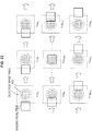
- FIGS. 13A to 13D are illustrative diagrams schematically showing examples of a light source provided in the imaging unit according to the present embodiment.
- FIG. 14 is an illustrative diagram schematically showing a structure of an image guide fiber provided in the imaging unit according to the present embodiment.
- FIGS. 15A to 15D are illustrative diagrams for describing mode excitation when light converges on an end face of a multi-mode optical waveguide.
- FIGS. 16A and 16B are illustrative diagrams schematically showing scanning methods of the image guide fiber of the imaging unit according to the present embodiment.
- FIG. 17 is an illustrative diagram schematically showing a specific example of the imaging unit according to the present embodiment.
- FIGS. 18A and 18B are illustrative diagrams for describing an end unit of the image guide fiber according to the present embodiment.
- the imaging unit 40 of the image acquisition system 30 mainly has a light source optical system 401, an image guide fiber 403, and an imaging optical system 405 as illustrated in FIG. 12 .
- the light source optical system 401 is an optical system which guides excitation light having a predetermined wavelength for generating fluorescence by exciting the measurement subject S with two or more photons (i.e., excitation using multiple photons) toward the measurement subject S.
- the light source optical system 401 is constituted by a laser light source which emits the excitation light having a predetermined wavelength and optical elements such as various lenses, various mirrors, and various filters that guide the excitation light emitted from the light source toward the measurement subject S.
- a detailed disposition of the various optical elements in the light source optical system 401 is not particularly limited, and a disposition of a known optical system can be employed.
- a laser light source of the light source optical system 401 is also not particularly limited, and any of a variety of light sources such as various semiconductor lasers, solid-state lasers, and gas lasers can be used.
- the image acquisition system 30 can be further miniaturized.
- a semiconductor laser and a light source which uses a wavelength conversion unit which converts a wavelength of light of the semiconductor laser as illustrated in FIG. 13A to 13D can be used, for example, as a light source which uses a semiconductor laser that can be used as the laser light source unit of the light source optical system 401.
- FIG. 13A schematically illustrates a master oscillator 411, which is constituted by a semiconductor laser and a resonator, as an example of a semiconductor laser that can be used in the laser light source unit.
- the master oscillator 411 provided as the laser light source unit is constituted by a semiconductor laser unit 412 that can emit laser light having a predetermined wavelength (e.g., a wavelength of 405 nm) and a resonator unit 413 for amplifying the laser light emitted from the semiconductor laser unit 412.
- a predetermined wavelength e.g., a wavelength of 405 nm
- FIG. 13B schematically illustrates a master oscillator power amplifier (MOPA) 414, which is constituted by a master oscillator and an optical amplifier, as an example of a semiconductor laser that can be used in the laser light source unit.
- MOPA master oscillator power amplifier
- an optical amplifier 415 for further amplifying the emitted laser light is provided in a later stage of the master oscillator 411 illustrated in FIG. 13A .
- a semiconductor optical amplifier (SOA) or the like can be preferably used, for example, as the optical amplifier 415.
- FIG. 13C schematically illustrates a light source, which has the MOPA 414 and a wavelength conversion unit, as an example of a semiconductor laser that can be used in the laser light source unit.
- a wavelength conversion unit 416 for converting a wavelength of laser light which has had its intensity amplified is provided in a later stage of the optical amplifier 415 illustrated in FIG. 13B .
- An optical parametric oscilator (OPO) which uses various types of non-linear crystals or the like can be preferably used, for example, as the wavelength conversion unit 416.
- OPO optical parametric oscilator
- wavelength conversion efficiency of the wavelength conversion unit 416 can be further improved.
- a wavelength of excitation light emitted from the laser light source is not particularly limited, and a wavelength suitable for exciting a fluorescent substance included in the measurement subject S may be appropriately selected.
- a laser to be used as the light source may be a continuous wave (CW) laser or a pulse laser.
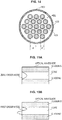
- the image guide fiber 403 is formed by bundling a plurality of multimode optical fiber element wires 421 as schematically illustrated in FIG. 14 .
- Each of the optical fiber element wires 421 is formed of a core 423 that can guide light of a zero-order mode but also light of a higher-order mode, and a cladding 425 provided to cover the core 423.
- the optical fiber element wires 421 are disposed to have a hexagonal close-packed structure as schematically illustrated in FIG. 14 so far as possible.
- a separation distance d between adjacent optical fiber element wires 421 may be appropriately set in accordance with image resolution to be obtained, and, for example, a value such as 3.5 ⁇ m may be possible.
- a diameter d' of the core 423 may also be appropriately set, and, for example, a value such as 3 ⁇ m may be possible.
- the image guide fiber 403 transmits excitation light from the light source optical system 401 incident on one end (e.g., an end A in FIG. 12 ) to the measurement subject S, and transmits an image of the measurement subject S formed on the other end (e.g., an end B in FIG. 12 ) using fluorescence generated from the measurement subject S to the one end (e.g., the end A in FIG. 12 ).
- the imaging optical system 405 scans the image of the measurement subject S transmitted to the end (e.g., the end A in FIG. 12 ) of the image guide fiber 403 at a scanning pitch that is narrower than a size of the core 423 (the core diameter d' in FIG. 14 ) of each of the plurality of optical fiber element wires 421. At this time, the imaging optical system 405 performs imaging such that at least a part of an optical fiber element wire-corresponding image which corresponds to each of the optical fiber element wires 421 is included in a plurality of images, and generates a plurality of pieces of image data of the measurement subject S.
- the imaging optical system 405 is constituted by various detectors which detect an image (i.e., a fluorescence signal corresponding to generated fluorescence) of the measurement subject S transmitted from the image guide fiber 403, and optical elements such as various lenses, various mirrors, various filters, and the like which guide the image (fluorescence signal) of the measurement subject S toward the detectors.
- a detailed disposition of the various optical elements of the imaging optical system 405 is not particularly limited, and a disposition of a known optical system can be employed.
- detectors can also be used as the detectors provided in the imaging optical system 405 as long as they can convert information regarding intensity of fluorescence into an electric signal.
- Various detectors such as a charge-coupled device (CCD), a photomultiplier tube (PMT), and the like can be exemplified, for example, as the detector.
- CCD charge-coupled device
- PMT photomultiplier tube
- a mechanism for scanning the end faces of the image guide fiber 403 as will be described in detail below is provided in at least any one of the light source optical system 401 and the imaging optical system 405 shown in FIG. 12 .
- a scanning mechanism is not particularly limited, and, for example, a known mechanism such as a galvano mirror can be used.
- the configuration of the imaging unit 40 according to the present embodiment has been described above in detail with reference to FIGS. 12 to 14 .
- the modes have orthogonality.
- perturbation caused from the outside for example, like when there is a flaw on the optical waveguide, is not exerted, propagation occurs on the optical waveguide (optical fiber) in the zero-order mode without change in the case of the zero-order mode, and propagation also occurs on the optical waveguide in the first-order mode without change in the case of the first-order mode.
- an electric field distribution of the convergence spot substantially matches an electric field distribution of the zero-order mode illustrated in FIG. 15A , and thus the zero-order mode is excited in the inside of the fiber.
- the electric field strength distribution illustrated in FIG. 15B has a different sign at the center, the electric field strength distribution illustrated in FIG. 15C and the electric field strength distribution of the first-order mode illustrated in FIG. 15B have an integrated value that is substantially zero, and thus the first-order mode is not excited.
- the convergence spot is shifted from the center of the core as illustrated in FIG.
- a convolution integral of the electric field strength distribution illustrated in FIG. 15D and the first-order mode illustrated in FIG. 15B are not zero, thus the first-order mode is excited at a certain ratio, and a ratio at which the zero-order mode is excited decreases accordingly.
- the zero-order mode is excited on the incident end face when the zero-order mode is dominantly excited on the incident end face as illustrated in FIG. 15C , and since the waveguide mode of the optical waveguide has orthogonality, light is guided toward the emission end inside the optical fiber without change in the zero-order mode.
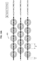
- the present inventor has ascertained that, if a single mode (the zero-order mode) is excited on an incident end face of an image guide fiber, a case in which light probably reaches the sample-side end face in a single mode exists, and thus the present inventor has conceived a scanning method for an end face of the image guide fiber 403 as schematically illustrated in FIGS. 16A and 16B .
- the imaging unit 40 scans an end face of the image guide fiber 403 (e.g., the end face of the end A in FIG. 12 ) at a scanning pitch that is narrower than a size of a core of each of a plurality of optical fiber element wires.
- FIG. 16A illustrates an example in which scanning is performed at a pitch p that is narrower than the size d' of a core of each optical fiber element wire 421 in a direction parallel to a scanning direction of an end face of the image guide fiber 403.
- a position of an axis expressing the scanning direction (a scanning axis) is set in advance in accordance with a diameter of the image guide fiber 403 to be used and the core diameter d' of each optical fiber element wire 421, and the end face of the image guide fiber 403 is captured at positions of black circles in FIG. 16A under control of the arithmetic processing unit 50.
- imaging intervals in the direction parallel to the scanning direction are controlled by the arithmetic processing unit 50 on the basis of the scanning pitch p
- imaging intervals in a direction orthogonal to the scanning direction are controlled on the basis of an interval d of the adjacent optical fiber element wires 421 of the image guide fiber 403.
- the entire measurement subject S is captured one time under the above-described control.
- a frequency of image data generated through imaging (a data restoration frequency) is higher than the number of optical fiber element wires 421.
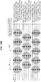
- FIG. 16B illustrates an example in which scanning is performed at the pitch p that is narrower than the size d' of the core of each of the optical fiber element wires 421 in the direction orthogonal to the scanning direction of an end face of the image guide fiber 403.
- a position of an axis expressing the scanning direction (a scanning axis) is set in advance in accordance with the diameter of the image guide fiber 403 to be used and the core diameter d' of each of the optical fiber element wires 421, and the end face of the image guide fiber 403 is captured at positions of black circles in FIG. 16B under control of the arithmetic processing unit 50.
- the imaging intervals in the direction parallel to the scanning direction are controlled by the arithmetic processing unit 50 on the basis of the interval d of the adjacent optical fiber element wires 421 of the image guide fiber 403, the imaging intervals in the direction orthogonal to the scanning direction are controlled on the basis of the scanning pitch p.
- the entire measurement subject S is captured a plurality of times (e.g., 5 times in the example of FIG. 16B ) under the above-described control.
- a frequency of data restoration in one scanning corresponds to the number of optical fiber element wires 421, and reference positions (scanning start positions) in each scanning process change at the pitch p that is narrower than a disposition pitch of the optical fiber element wires 421.
- imaging in the above description means forming an image at the position of the black circles in FIGS. 16A and 16B with excitation light guided by the light source optical system 401, and capturing an image (a fluorescence image) transmitted to an end face of the image guide fiber 403 at the positions of the black circles.
- optical fiber element wires-corresponding area As the above-described scanning method is realized, at least a part of areas corresponding to the optical fiber element wires 421 (which will also be referred to as an "optical fiber element wires-corresponding area" below) is captured and included in a plurality of images.
- a plurality of pieces of image data generated through imaging processes include image data of a case in which excitation light is radiated to all cores.
- a fundamental wave (the zero-order mode) is excited at the core of the image guide fiber 403, and thus there also is a case in which the fundamental wave probably reaches a sample-side end face.
- the imaging unit 40 may perform an imaging process only one time at each of the imaging positions illustrated in FIGS. 16A and 16B , and may perform the imaging process a plurality of times at each of the imaging positions to increase a probability.
- the imaging unit 40 may employ a scanning method obtained by combining the methods of FIG. 16A and FIG. 16B (i.e., the scanning methods at the scanning pitch p in the scanning direction and the direction orthogonal to the scanning direction).
- a specific size of the scanning pitch p shown in FIGS. 16A and 16B may be appropriately set in accordance with the core diameter d' of the optical fiber element wire 421, and a size of about 1/10 of the core diameter d' or smaller is preferable.
- the scanning pitch p by setting the scanning pitch p to be 1/10 of the core diameter d' or smaller, (e.g., when the core diameter d' is 3 ⁇ m, the scanning pitch p is set to be 0.3 ⁇ m or smaller), it is possible to obtain luminance of 86% or more of the maximum luminance obtained through excitation by the optical fiber element wires 421.
- the scanning pitch p to be 1/12 of the core diameter of d' or smaller, it is possible to obtain luminance of 90% or more of the maximum luminance obtained through excitation by the optical fiber element wires 421.
- FIGS. 16A and 16B the scanning directions and imaging positions shown in FIGS. 16A and 16B and the number of scanning operations shown in FIG. 16B are merely examples, and the present invention is not limited to the examples shown in FIGS. 16A and 16B .
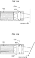
- FIGS. 17 to 18B A specific example of the imaging unit 40 according to the present embodiment will be briefly described with reference to FIGS. 17 to 18B .
- excitation light computed from one of the light sources illustrated in FIGS. 13A to 13D is guided toward an XY galvano mirror XY-gal via a lens L and a mirror M, and the galvano mirror controls an image formation position with respect to the image guide fiber 403.
- Excitation light that has gone through the galvano mirror goes through a relay lens RL, the mirror M, and a dichroic mirror DM, and is guided to an object lens Obj.
- one end of the above-described image guide fiber 403 is arranged at a focal position f of the object lens Obj.
- Fluorescence is generated from the measurement subject S by the excitation light that has passed through the image guide fiber 403 and the end unit 431 and has been guided to the measurement subject S.
- the generated fluorescence passes through the end unit 431, the image guide fiber 403, the object lens Obj, the dichroic mirror DM, another lens L, a notch filter F, and the like, and is guided to a photomultiplier serving as a detector or the like.
- the imaging unit 40 it is important to acquire fluorescence images while changing a position of the measurement subject S in the thickness direction (i.e., changing a focal position thereof).
- a position of the measurement subject S in the thickness direction i.e., changing a focal position thereof.
- moving a lens 433 installed at a leading end of the optical fiber element wires 421 in the end unit 431 or moving the whole end unit 431 to move a coupling face of the lens 433 as illustrated in FIG. 18A is considered. Accordingly, it is possible to acquire fluorescence images which have different observation positions in the depth direction.
- an optical component 435 for a hologram that can simultaneously acquire fluorescence from different thickness positions of the measurement subject S between the optical fiber element wires 421 and the lens 433 as illustrated in FIG. 18B .
- a spatial light modulator (SLM) disclosed in Non-Patent Literatures 2 and 3, a quadratically distorted grating disclosed in Non-Patent Literature 4, or the like can be exemplified, for example, as the optical component 435.
- an amount of information regarding the fluorescence at the thickness positions is smaller than the case in which the end unit 431 is used as illustrated in FIG. 18A .
- it is preferable to increase an amount of information regarding the fluorescence at the thickness positions by using the image guide fiber 403 that has as many pixels as possible or by rotating the image guide fiber 403 and then reacquiring the images. Note that, when the image guide fiber 403 is rotated, a direction in which the thickness positions are different is also rotated in accordance with the rotation of the image guide fiber 403 without needing to provide a driving mechanism in the end unit 431.
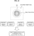
- FIG. 19 is a block diagram schematically showing a configuration of the arithmetic processing unit included in the image acquisition system according to the present embodiment.
- FIG. 20 is a block diagram showing an example of a configuration of a data processing unit according to the present embodiment.
- FIGS. 21 to 23 are illustrative diagrams for describing a representative pixel value selection process of the arithmetic processing unit according to the present embodiment.
- the arithmetic processing unit 50 is a unit which controls operations of the imaging unit 40 and performs a predetermined arithmetic process on image data generated by the imaging unit 40, and thereby generates a plurality of fluorescence images each corresponding to thickness positions of the measurement subject S.
- the arithmetic processing unit 50 mainly has an imaging unit control unit 501, a data acquisition unit 503, a data processing unit 505, a display control unit 507, and a storage unit 509 as schematically illustrated in FIG. 19 .
- the imaging unit control unit 501 is realized by, for example, a CPU, a ROM, a RAM, a communication device, and the like.
- the imaging unit control unit 501 transmits and receives various control signals to and from the light source, the optical elements, the scanning mechanism, and the like constituting the imaging unit 40 according to the present embodiment, and thereby generally manages various operations of the imaging unit 40. Accordingly, the light source of the imaging unit 40 emits excitation light at a predetermined timing, or an end face of the image guide fiber 403 is scanned on the basis of the above-described scanning methods.
- the light source, the optical elements, the scanning mechanism, and the like constituting the imaging unit 40 may also be able to perform various kinds of control while cooperating with each other via the imaging unit control unit 501.
- various kinds of control information to be used when the imaging unit control unit 501 controls the imaging unit 40 e.g., information regarding an imaging position and the like
- various kinds of control information to be used when the imaging unit control unit 501 controls the imaging unit 40 are output to the data acquisition unit 503, the data processing unit 505, and the like when necessary and are appropriately used in various processes performed in the processing units.
- the imaging unit control unit 501 may control power of excitation light radiated toward the measurement subject S using information regarding a scattering coefficient of the measurement subject S computed by the data processing unit 505 to be described below.
- the data acquisition unit 503 is realized by, for example, a CPU, a ROM, a RAM, a communication device, and the like.
- the data acquisition unit 503 acquires a plurality of pieces of image data generated by the imaging unit 40 on the basis of the above-described scanning methods from the imaging unit 40.
- the plurality of pieces of image data acquired by the data acquisition unit 503 are transmitted to the data processing unit 505 to be described below.
- the data acquisition unit 503 may associate the acquired plurality of pieces of image data with time information regarding a date, time and the like at which the image data was acquired, and may store the associated data in the storage unit 509 to be described below as history information.
- the data processing unit 505 is realized by, for example, a CPU, a ROM, a RAM, and the like.
- the data processing unit 505 generates fluorescence images of the measurement subject S by performing various data processes on the plurality of images captured by the imaging unit 40 transmitted from the data acquisition unit 503, and specifies a position of a surface and the scattering coefficient of the measurement subject S further using the obtained fluorescence images.
- the data processing unit 505 outputs the generated fluorescence images and the computed information regarding image information to the display control unit 507.
- the fluorescence images of the measurement subject S and the image information regarding the fluorescence images are output to a display unit (not illustrated) of the arithmetic processing unit 50 or any of a variety of computers and the like that can communicate with the arithmetic processing unit 50.
- the data processing unit 505 may output the obtained fluorescence images and image information to various recording media, various computers, and the like, or may output the obtained fluorescence images and image information to a paper medium or the like using an output device such as a printer.
- the data processing unit 505 may associate the fluorescence images of the measurement subject S and the image information regarding the fluorescence images with time information regarding a date, time, and the like at which the information was computed and store the associated data in the storage unit 509 as history information.
- the display control unit 507 is realized by, for example, a CPU, a ROM, a RAM, an output device, and the like.
- the display control unit 507 performs display control to display the fluorescence images of the measurement subject S, the position of the surface of the measurement subject S, and various processing results including information regarding the scattering coefficient and the like of the measurement subject S transmitted from the data processing unit 505 on an output device such as a display provided in the arithmetic processing unit 50, an output device provided outside of the arithmetic processing unit 50, or the like. Accordingly, a user of the image acquisition system 30 can immediately ascertain various processing results with regard to the measurement subject S.
- the storage unit 509 is realized by, for example, a RAM, a storage device, or the like provided in the arithmetic processing unit 50 according to the present embodiment.
- the storage unit 509 appropriately records various parameters and process developments that need to be saved by the arithmetic processing unit 50 according to the present embodiment to perform any process or various databases, programs, and the like.
- the storage unit 509 enables the imaging unit control unit 501, the data acquisition unit 503, the data processing unit 505, the display control unit 507, and the like to freely perform data read and write processes.
- the data processing unit 505 is provided with a selection unit 511, a captured image re-constructing unit 513, a representative luminance value specifying unit 515, a surface position specifying unit 517, a scattering coefficient computation unit 519, and a result output unit 521 as illustrated in FIG. 20 .
- the selection unit 511 is realized by, for example, a CPU, a ROM, a RAM, and the like.
- the selection unit 511 selects, for each of a plurality of pixels constituting an optical fiber element wire-corresponding area, a pixel value that is maximum luminance of a plurality of pieces of image data transmitted from the data acquisition unit 503 as a representative pixel value of the pixel.
- a process of selecting a representative pixel value executed by the selection unit 511 will be described in detail below with reference to FIGS. 21 to 23 .
- the image guide fiber 403 is formed by bundling a plurality of optical fiber element wires 421, an optical fiber element wire-corresponding area, which is an area corresponding to one of the optical fiber element wires 421, can be virtually defined on the basis of the interval (the disposition pitch) d between adjacent optical fiber element wires and the core diameter d' of the optical fiber element wire 421 as schematically illustrated in FIG. 21 .
- the selection unit 511 deals with the optical fiber element wire-corresponding area defined for each of the optical fiber element wires 421 as a selection target area in the process for selecting a representative pixel value as will be described in detail below.
- an imaging visual field of a detector provided in the imaging optical system 405 moves in a certain selection target area in accordance with the elapse of time as schematically illustrated in FIG. 22 .
- the selection unit 511 refers to the luminance value at positions of a plurality of pieces of image data including a pixel to be noted for each of pixels constituting the selection target area and specifies the highest luminance value. Then, the selection unit 511 uses the specified highest luminance value as a representative pixel value of the pixel to be noted.
- the N pieces of image data are searched transversally, and image data that gives a highest luminance value L MAX is used as image data of the pixels to be noted.
- image data k is used as image data that gives a representative pixel value of the pixels to be noted.
- the selection unit 511 executes the process for selecting a representative pixel value described above for all selection target areas (i.e., all optical fiber element wire-corresponding areas).
- the selection unit 511 may select image data that gives a luminance value approximate to the highest luminance value instead of image data giving the highest luminance value.
- the selection unit 511 may specify the highest luminance value by comparing data of neighboring pixels and performing a filtering process of selecting a maximum luminance value of an optical fiber element wire-corresponding area.
- a filtering process for example, an ordinary filtering for an area of 10 pixels ⁇ 10 pixels or the like can be exemplified. Using the filtering process, the highest luminance value of pixels to be noted can be more quickly and easily searched for.
- the selection unit 511 When a representative pixel value is selected using the above-described method, the selection unit 511 outputs information regarding the selected representative pixel value to the captured image re-constructing unit 513.
- the captured image re-constructing unit 513 is realized by, for example, a CPU, a ROM, a RAM, and the like.
- the captured image re-constructing unit 513 re-constructs captured images of the imaging subject S using the selected representative pixel value. Accordingly, a fluorescence image of the measurement subject S expressing a state of fluorescence generated through the multi-photon excitation process can be generated.
- the captured image re-constructing unit 513 may cause a blur filter represented by a Gaussian filter to act on the generated fluorescence image of the measurement subject S. Accordingly, a fluorescence image in which the selected representative pixel value is more smoothly connected can be obtained.
- the captured image re-constructing unit 513 may execute known post-processing other than the above processes on the generated fluorescence image.
- the captured image re-constructing unit 513 outputs the fluorescence image generated as described above to the representative luminance value specifying unit 515 and the result output unit 521.
- the representative luminance value specifying unit 515, the surface position specifying unit 517, and the scattering coefficient computation unit 519 each have similar configurations and exhibit similar effects to those of the representative luminance value specifying unit 111, the surface position specifying unit 113, and the scattering coefficient computation unit 115 provided in the information processing device 10 according to the first embodiment of the present disclosure, and thus detailed description thereof will be omitted below.
- the result output unit 521 is realized by, for example, a CPU, a ROM, a RAM, a communication device, and the like.
- the result output unit 521 outputs the fluorescence image generated by the captured image re-constructing unit 513, information regarding a position of a surface of the measurement subject S specified by the surface position specifying unit 517, or information regarding the scattering coefficient R S of the measurement subject S computed by the scattering coefficient computation unit 519.
- the respective constituent elements may be configured using universal members and circuits, or may be configured using hardware specialized for the functions of the constituent elements.
- all of the functions of the constituent elements may be fulfilled by a CPU and the like.
- a configuration to be used can be appropriately changed in accordance with a technical level of any occasion at which the present embodiment is implemented.
- a computer program for realizing each function of the arithmetic processing unit according to the present embodiment described above can be produced and installed in personal computers and the like.
- a computer-readable recording medium on which the computer program is stored can also be provided.
- the recording medium is, for example, a magnetic disk, an optical disc, a magneto-optical disc, a flash memory, or the like.
- the computer program may be distributed through, for example, a network, without using a recording medium.
- FIG. 24 is a block diagram for illustrating the hardware configuration of the information processing device 10 and the arithmetic processing unit 50 according to the embodiment of the present disclosure.
- the information processing device 10 and the arithmetic processing unit 50 mainly include a CPU 901, a ROM 903, and a RAM 905. Furthermore, the arithmetic processing device 20 also includes a host bus 907, a bridge 909, an external bus 911, an interface 913, an input device 915, an output device 917, a storage device 919, a drive 921, a connection port 923, and a communication device 925.
- the CPU 901 serves as an arithmetic processing device and a control device, and controls the overall operation or a part of the operation of the information processing device 10 and the arithmetic processing unit 50 according to various programs recorded in the ROM 903, the RAM 905, the storage device 919, or a removable recording medium 927.
- the ROM 903 stores programs, operation parameters, and the like used by the CPU 901.
- the RAM 905 primarily stores programs used in execution of the CPU 901 and parameters and the like varying as appropriate during the execution. These are connected with each other via the host bus 907 configured from an internal bus such as a CPU bus or the like.
- the host bus 907 is connected to the external bus 911 such as a PCI (Peripheral Component Interconnect/Interface) bus via the bridge 909.
- PCI Peripheral Component Interconnect/Interface
- the input device 915 is an operation means operated by a user, such as a mouse, a keyboard, a touch panel, buttons, a switch and a lever. Also, the input device 915 may be a remote control means (a so-called remote control) using, for example, infrared light or other radio waves, or may be an externally connected device 929 such as a mobile phone or a PDA conforming to the operation of the information processing device 10 and the arithmetic processing unit 50. Furthermore, the input device 915 generates an input signal based on, for example, information which is input by a user with the above operation means, and is configured from an input control circuit for outputting the input signal to the CPU 901. The user can input various data to the information processing device 10 and the arithmetic processing unit 50 and can instruct the information processing device 10 and the arithmetic processing unit 50 to perform processing by operating this input device 915.
- a remote control means a so-called remote control
- the input device 915 generates an input signal based on, for
- the output device 917 is configured from a device capable of visually or audibly notifying acquired information to a user.
- Examples of such device include display devices such as a CRT display device, a liquid crystal display device, a plasma display device, an EL display device and lamps, audio output devices such as a speaker and a headphone, a printer, a mobile phone, a facsimile machine, and the like.
- the output device 917 outputs a result obtained by various processings performed by the information processing device 10 and the arithmetic processing unit 50. More specifically, the display device displays, in the form of texts or images, a result obtained by various processes performed by the information processing device 10 and the arithmetic processing unit 50.
- the audio output device converts an audio signal such as reproduced audio data and sound data into an analog signal, and outputs the analog signal.
- the storage device 919 is a device for storing data configured as an example of a storage unit of the information processing device 10 and the arithmetic processing unit 50 and is used to store data.
- the storage device 919 is configured from, for example, a magnetic storage device such as a HDD (Hard Disk Drive), a semiconductor storage device, an optical storage device, or a magneto-optical storage device.
- This storage device 919 stores programs to be executed by the CPU 901, various data, and sound signal data, image signal data, or the like, obtained externally.
- the drive 921 is a reader/writer for recording medium, and is embedded in the information processing device 10 and the arithmetic processing unit 50 or attached externally thereto.
- the drive 921 reads information recorded in the attached removable recording medium 927 such as a magnetic disk, an optical disk, a magneto-optical disk, or a semiconductor memory, and outputs the read information to the RAM 905.
- the drive 921 can write in the attached removable recording medium 927 such as a magnetic disk, an optical disk, a magneto-optical disk, or a semiconductor memory.
- the removable recording medium 927 is, for example, a DVD medium, an HD-DVD medium, or a Blu-ray (registered trademark) medium.
- the removable recording medium 927 may be a CompactFlash (CF; registered trademark), a flash memory, an SD memory card (Secure Digital Memory Card), or the like.
- the removable recording medium 927 may be, for example, an IC card (Integrated Circuit Card) equipped with a non-contact IC chip or an electronic appliance.
- connection port 923 is a port for allowing devices to directly connect to the information processing device 10 and the arithmetic processing unit 50.
- Examples of the connection port 923 include a USB (Universal Serial Bus) port, an IEEE1394 port, a SCSI (Small Computer System Interface) port, and the like.
- Other examples of the connection port 923 include an RS-232C port, an optical audio terminal, an HDMI (High-Definition Multimedia Interface) port, and the like.
- the information processing device 10 and the arithmetic processing unit 50 directly obtains sound signal data, image signal data, or the like, from the externally connected device 929 and provides sound signal data, image signal data, or the like, to the externally connected device 929.
- the communication device 925 is a communication interface configured from, for example, a communication device for connecting to a communication network 931.
- the communication device 925 is, for example, a wired or wireless LAN (Local Area Network), Bluetooth (registered trademark), a communication card for WUSB (Wireless USB), or the like.
- the communication device 925 may be a router for optical communication, a router for ADSL (Asymmetric Digital Subscriber Line), a modem for various communications, or the like.
- This communication device 925 can transmit and receive signals and the like in accordance with a predetermined protocol such as TCP/IP on the Internet and with other communication devices, for example.
- the communication network 931 connected to the communication device 925 is configured from a network and the like, which is connected via wire or wirelessly, and may be, for example, the Internet, a home LAN, infrared communication, radio wave communication, satellite communication, or the like.
- each of the structural elements described above may be configured using a general-purpose material, or may be configured from hardware dedicated to the function of each structural element. Accordingly, the hardware configuration to be used can be changed as appropriate according to the technical level at the time of carrying out the present embodiment.
Landscapes
- Health & Medical Sciences (AREA)
- Physics & Mathematics (AREA)
- Life Sciences & Earth Sciences (AREA)
- Optics & Photonics (AREA)
- Engineering & Computer Science (AREA)
- Surgery (AREA)
- General Physics & Mathematics (AREA)
- Pathology (AREA)
- General Health & Medical Sciences (AREA)
- Chemical & Material Sciences (AREA)
- Analytical Chemistry (AREA)
- Nuclear Medicine, Radiotherapy & Molecular Imaging (AREA)
- Public Health (AREA)
- Veterinary Medicine (AREA)
- Biophysics (AREA)
- Biomedical Technology (AREA)
- Heart & Thoracic Surgery (AREA)
- Medical Informatics (AREA)
- Molecular Biology (AREA)
- Animal Behavior & Ethology (AREA)
- Radiology & Medical Imaging (AREA)
- Multimedia (AREA)
- Immunology (AREA)
- Biochemistry (AREA)
- Signal Processing (AREA)
- Spectroscopy & Molecular Physics (AREA)
- Computer Vision & Pattern Recognition (AREA)
- Theoretical Computer Science (AREA)
- Investigating, Analyzing Materials By Fluorescence Or Luminescence (AREA)
- Microscoopes, Condenser (AREA)
- Endoscopes (AREA)
Applications Claiming Priority (2)
| Application Number | Priority Date | Filing Date | Title |
|---|---|---|---|
| JP2014248009A JP2016109579A (ja) | 2014-12-08 | 2014-12-08 | 情報処理装置、画像取得システム、情報処理方法、画像情報取得方法及びプログラム |
| PCT/JP2015/077855 WO2016092940A1 (ja) | 2014-12-08 | 2015-09-30 | 情報処理装置、画像取得システム、情報処理方法、画像情報取得方法及びプログラム |
Publications (3)
| Publication Number | Publication Date |
|---|---|
| EP3232181A1 EP3232181A1 (en) | 2017-10-18 |
| EP3232181A4 EP3232181A4 (en) | 2018-08-08 |
| EP3232181B1 true EP3232181B1 (en) | 2020-09-02 |
Family
ID=56107135
Family Applications (1)
| Application Number | Title | Priority Date | Filing Date |
|---|---|---|---|
| EP15866785.7A Active EP3232181B1 (en) | 2014-12-08 | 2015-09-30 | Information processing device, information acquisition system, information processing method, image information acquisition method, and program |
Country Status (4)
| Country | Link |
|---|---|
| US (2) | US10190982B2 (ja) |
| EP (1) | EP3232181B1 (ja) |
| JP (1) | JP2016109579A (ja) |
| WO (1) | WO2016092940A1 (ja) |
Families Citing this family (6)
| Publication number | Priority date | Publication date | Assignee | Title |
|---|---|---|---|---|
| JP2016109579A (ja) * | 2014-12-08 | 2016-06-20 | ソニー株式会社 | 情報処理装置、画像取得システム、情報処理方法、画像情報取得方法及びプログラム |
| EP3165153A1 (en) * | 2015-11-05 | 2017-05-10 | Deutsches Krebsforschungszentrum Stiftung des Öffentlichen Rechts | System for fluorescence aided surgery |
| CN107621463B (zh) * | 2017-10-16 | 2024-03-22 | 苏州微景医学科技有限公司 | 图像重建方法、装置及显微成像装置 |
| JP6986452B2 (ja) | 2018-01-04 | 2021-12-22 | 浜松ホトニクス株式会社 | 蛍光測定装置および蛍光測定方法 |
| WO2020003429A1 (ja) | 2018-06-28 | 2020-01-02 | オリンパス株式会社 | 光走査装置及び撮像装置 |
| JP7158220B2 (ja) * | 2018-09-11 | 2022-10-21 | 浜松ホトニクス株式会社 | 測定装置および測定方法 |
Family Cites Families (15)
| Publication number | Priority date | Publication date | Assignee | Title |
|---|---|---|---|---|
| JPH04138127A (ja) * | 1990-09-28 | 1992-05-12 | Olympus Optical Co Ltd | 内視鏡網目画像軽減装置 |
| JP2568337B2 (ja) * | 1991-11-01 | 1997-01-08 | フクダ電子株式会社 | 実時間内視画像処理方式 |
| JPH11108615A (ja) | 1997-10-01 | 1999-04-23 | Asahi Glass Co Ltd | 鏡面材料並びに透光性材料の表面位置検出方法及び装置 |
| WO2002048693A1 (fr) * | 2000-12-14 | 2002-06-20 | Olympus Optical Co., Ltd. | Analyseur fluorometrique et analyse fluorometrique |
| US7756305B2 (en) | 2002-01-23 | 2010-07-13 | The Regents Of The University Of California | Fast 3D cytometry for information in tissue engineering |
| JP5278854B2 (ja) | 2007-12-10 | 2013-09-04 | 富士フイルム株式会社 | 画像処理システムおよびプログラム |
| JP2010284369A (ja) | 2009-06-12 | 2010-12-24 | Fujifilm Corp | 内視鏡システム、内視鏡、並びに内視鏡駆動方法 |
| JP5293468B2 (ja) * | 2009-07-10 | 2013-09-18 | ソニー株式会社 | 蛍光像取得装置、蛍光像取得方法及び蛍光像取得プログラム |
| DE202010010932U1 (de) * | 2010-04-19 | 2011-10-07 | Witec Wissenschaftliche Instrumente Und Technologie Gmbh | Vorrichtung zur Abbildung einer Probenoberfläche |
| JP6230912B2 (ja) | 2010-10-14 | 2017-11-15 | コーニンクレッカ フィリップス エヌ ヴェKoninklijke Philips N.V. | 物体の特性を決定する特性決定装置 |
| JP5829030B2 (ja) * | 2011-03-23 | 2015-12-09 | オリンパス株式会社 | 顕微鏡 |
| JP2013011527A (ja) * | 2011-06-29 | 2013-01-17 | Olympus Corp | 蛍光顕微鏡システムおよび蛍光物質の定量方法 |
| JP2013058956A (ja) * | 2011-09-09 | 2013-03-28 | Sony Corp | 情報処理装置、情報処理方法、プログラム及び情報処理システム |
| DE102013208927A1 (de) * | 2013-05-14 | 2014-11-20 | Carl Zeiss Microscopy Gmbh | Verfahren zur 3D-hochauflösenden Lokalisierungsmikroskopie |
| JP2016109579A (ja) * | 2014-12-08 | 2016-06-20 | ソニー株式会社 | 情報処理装置、画像取得システム、情報処理方法、画像情報取得方法及びプログラム |
-
2014
- 2014-12-08 JP JP2014248009A patent/JP2016109579A/ja active Pending
-
2015
- 2015-09-30 US US15/529,790 patent/US10190982B2/en active Active
- 2015-09-30 WO PCT/JP2015/077855 patent/WO2016092940A1/ja active Application Filing
- 2015-09-30 EP EP15866785.7A patent/EP3232181B1/en active Active
-
2018
- 2018-12-13 US US16/218,764 patent/US10753871B2/en active Active
Non-Patent Citations (1)
| Title |
|---|
| None * |
Also Published As
| Publication number | Publication date |
|---|---|
| US20190113454A1 (en) | 2019-04-18 |
| US10190982B2 (en) | 2019-01-29 |
| JP2016109579A (ja) | 2016-06-20 |
| EP3232181A1 (en) | 2017-10-18 |
| US10753871B2 (en) | 2020-08-25 |
| US20170315056A1 (en) | 2017-11-02 |
| EP3232181A4 (en) | 2018-08-08 |
| WO2016092940A1 (ja) | 2016-06-16 |
Similar Documents
| Publication | Publication Date | Title |
|---|---|---|
| US10753871B2 (en) | Information processing device, image acquisition system, information processing method, and image information acquisition method | |
| Gorpas et al. | Autofluorescence lifetime augmented reality as a means for real-time robotic surgery guidance in human patients | |
| JP7217893B2 (ja) | 光学組織像の分析及び遠隔読影のためのシステム及び方法 | |
| JP6416887B2 (ja) | 構造化照明を用いた組織試料の顕微鏡観察 | |
| WO2020139835A1 (en) | Systems and methods for two-dimensional fluorescence wave propagation onto surfaces using deep learning | |
| JP6587004B2 (ja) | 装置、システム、方法、及びプログラム | |
| JP7482894B2 (ja) | 組織における術中造影剤の検出のための撮像システム | |
| JP5185151B2 (ja) | 顕微鏡観察システム | |
| Zirak et al. | Invited Article: A rigid coherent anti-Stokes Raman scattering endoscope with high resolution and a large field of view | |
| US9632300B2 (en) | Image processing apparatus, microscope system, image processing method, and computer-readable recording medium | |
| Tate et al. | Multispectral fluorescence imaging of human ovarian and fallopian tube tissue for early-stage cancer detection | |
| US20180246309A1 (en) | Scan-based imaging with variable scan speed using predictions of region-of-interest positions | |
| JP4539342B2 (ja) | 解析装置、顕微鏡、および、解析プログラム | |
| Harris et al. | A pulse coupled neural network segmentation algorithm for reflectance confocal images of epithelial tissue | |
| Chen et al. | High-resolution two-photon transcranial imaging of brain using direct wavefront sensing | |
| Adur et al. | The severity of Osteogenesis imperfecta and type I collagen pattern in human skin as determined by nonlinear microscopy: proof of principle of a diagnostic method | |
| JP2007215419A (ja) | 細胞状態検出装置及び方法 | |
| Pham et al. | Feasibility of multimodal multiphoton microscopy to facilitate surgical margin assessment in pancreatic cancer | |
| Legesse et al. | Hepatic Vitamin A Content Investigation Using Coherent Anti‐Stokes Raman Scattering Microscopy | |
| Breunig et al. | Rapid vertical tissue imaging with clinical multiphoton tomography | |
| Chen et al. | Generative adversarial network improves the resolution of pulsed STED microscopy | |
| Xie et al. | Multi-scale spectrally resolved quantitative fluorescence imaging system: towards neurosurgical guidance in glioma resection | |
| Huang et al. | Ultraviolet Photoacoustic Microscopy for Histopathology | |
| WO2015182269A1 (ja) | 画像取得装置及び画像取得方法 | |
| Sampson | Optical bioimaging 2010: seeing more, deeper, faster |
Legal Events
| Date | Code | Title | Description |
|---|---|---|---|
| STAA | Information on the status of an ep patent application or granted ep patent |
Free format text: STATUS: THE INTERNATIONAL PUBLICATION HAS BEEN MADE |
|
| PUAI | Public reference made under article 153(3) epc to a published international application that has entered the european phase |
Free format text: ORIGINAL CODE: 0009012 |
|
| STAA | Information on the status of an ep patent application or granted ep patent |
Free format text: STATUS: REQUEST FOR EXAMINATION WAS MADE |
|
| 17P | Request for examination filed |
Effective date: 20170601 |
|
| AK | Designated contracting states |
Kind code of ref document: A1 Designated state(s): AL AT BE BG CH CY CZ DE DK EE ES FI FR GB GR HR HU IE IS IT LI LT LU LV MC MK MT NL NO PL PT RO RS SE SI SK SM TR |
|
| AX | Request for extension of the european patent |
Extension state: BA ME |
|
| DAV | Request for validation of the european patent (deleted) | ||
| DAX | Request for extension of the european patent (deleted) | ||
| A4 | Supplementary search report drawn up and despatched |
Effective date: 20180709 |
|
| RIC1 | Information provided on ipc code assigned before grant |
Ipc: G02B 21/36 20060101ALI20180703BHEP Ipc: G02B 21/06 20060101ALI20180703BHEP Ipc: G01N 21/64 20060101AFI20180703BHEP Ipc: A61B 1/00 20060101ALI20180703BHEP |
|
| GRAP | Despatch of communication of intention to grant a patent |
Free format text: ORIGINAL CODE: EPIDOSNIGR1 |
|
| STAA | Information on the status of an ep patent application or granted ep patent |
Free format text: STATUS: GRANT OF PATENT IS INTENDED |
|
| INTG | Intention to grant announced |
Effective date: 20200324 |
|
| GRAS | Grant fee paid |
Free format text: ORIGINAL CODE: EPIDOSNIGR3 |
|
| GRAA | (expected) grant |
Free format text: ORIGINAL CODE: 0009210 |
|
| STAA | Information on the status of an ep patent application or granted ep patent |
Free format text: STATUS: THE PATENT HAS BEEN GRANTED |
|
| AK | Designated contracting states |
Kind code of ref document: B1 Designated state(s): AL AT BE BG CH CY CZ DE DK EE ES FI FR GB GR HR HU IE IS IT LI LT LU LV MC MK MT NL NO PL PT RO RS SE SI SK SM TR |
|
| REG | Reference to a national code |
Ref country code: GB Ref legal event code: FG4D |
|
| REG | Reference to a national code |
Ref country code: AT Ref legal event code: REF Ref document number: 1309414 Country of ref document: AT Kind code of ref document: T Effective date: 20200915 Ref country code: CH Ref legal event code: EP |
|
| REG | Reference to a national code |
Ref country code: DE Ref legal event code: R096 Ref document number: 602015058593 Country of ref document: DE |
|
| REG | Reference to a national code |
Ref country code: IE Ref legal event code: FG4D |
|
| REG | Reference to a national code |
Ref country code: LT Ref legal event code: MG4D |
|
| PG25 | Lapsed in a contracting state [announced via postgrant information from national office to epo] |
Ref country code: FI Free format text: LAPSE BECAUSE OF FAILURE TO SUBMIT A TRANSLATION OF THE DESCRIPTION OR TO PAY THE FEE WITHIN THE PRESCRIBED TIME-LIMIT Effective date: 20200902 Ref country code: HR Free format text: LAPSE BECAUSE OF FAILURE TO SUBMIT A TRANSLATION OF THE DESCRIPTION OR TO PAY THE FEE WITHIN THE PRESCRIBED TIME-LIMIT Effective date: 20200902 Ref country code: SE Free format text: LAPSE BECAUSE OF FAILURE TO SUBMIT A TRANSLATION OF THE DESCRIPTION OR TO PAY THE FEE WITHIN THE PRESCRIBED TIME-LIMIT Effective date: 20200902 Ref country code: LT Free format text: LAPSE BECAUSE OF FAILURE TO SUBMIT A TRANSLATION OF THE DESCRIPTION OR TO PAY THE FEE WITHIN THE PRESCRIBED TIME-LIMIT Effective date: 20200902 Ref country code: BG Free format text: LAPSE BECAUSE OF FAILURE TO SUBMIT A TRANSLATION OF THE DESCRIPTION OR TO PAY THE FEE WITHIN THE PRESCRIBED TIME-LIMIT Effective date: 20201202 Ref country code: GR Free format text: LAPSE BECAUSE OF FAILURE TO SUBMIT A TRANSLATION OF THE DESCRIPTION OR TO PAY THE FEE WITHIN THE PRESCRIBED TIME-LIMIT Effective date: 20201203 Ref country code: NO Free format text: LAPSE BECAUSE OF FAILURE TO SUBMIT A TRANSLATION OF THE DESCRIPTION OR TO PAY THE FEE WITHIN THE PRESCRIBED TIME-LIMIT Effective date: 20201202 |
|
| REG | Reference to a national code |
Ref country code: NL Ref legal event code: MP Effective date: 20200902 |
|
| REG | Reference to a national code |
Ref country code: AT Ref legal event code: MK05 Ref document number: 1309414 Country of ref document: AT Kind code of ref document: T Effective date: 20200902 |
|
| PG25 | Lapsed in a contracting state [announced via postgrant information from national office to epo] |
Ref country code: LV Free format text: LAPSE BECAUSE OF FAILURE TO SUBMIT A TRANSLATION OF THE DESCRIPTION OR TO PAY THE FEE WITHIN THE PRESCRIBED TIME-LIMIT Effective date: 20200902 Ref country code: RS Free format text: LAPSE BECAUSE OF FAILURE TO SUBMIT A TRANSLATION OF THE DESCRIPTION OR TO PAY THE FEE WITHIN THE PRESCRIBED TIME-LIMIT Effective date: 20200902 Ref country code: PL Free format text: LAPSE BECAUSE OF FAILURE TO SUBMIT A TRANSLATION OF THE DESCRIPTION OR TO PAY THE FEE WITHIN THE PRESCRIBED TIME-LIMIT Effective date: 20200902 |
|
| PG25 | Lapsed in a contracting state [announced via postgrant information from national office to epo] |
Ref country code: EE Free format text: LAPSE BECAUSE OF FAILURE TO SUBMIT A TRANSLATION OF THE DESCRIPTION OR TO PAY THE FEE WITHIN THE PRESCRIBED TIME-LIMIT Effective date: 20200902 Ref country code: SM Free format text: LAPSE BECAUSE OF FAILURE TO SUBMIT A TRANSLATION OF THE DESCRIPTION OR TO PAY THE FEE WITHIN THE PRESCRIBED TIME-LIMIT Effective date: 20200902 Ref country code: PT Free format text: LAPSE BECAUSE OF FAILURE TO SUBMIT A TRANSLATION OF THE DESCRIPTION OR TO PAY THE FEE WITHIN THE PRESCRIBED TIME-LIMIT Effective date: 20210104 Ref country code: RO Free format text: LAPSE BECAUSE OF FAILURE TO SUBMIT A TRANSLATION OF THE DESCRIPTION OR TO PAY THE FEE WITHIN THE PRESCRIBED TIME-LIMIT Effective date: 20200902 Ref country code: CZ Free format text: LAPSE BECAUSE OF FAILURE TO SUBMIT A TRANSLATION OF THE DESCRIPTION OR TO PAY THE FEE WITHIN THE PRESCRIBED TIME-LIMIT Effective date: 20200902 |
|
| REG | Reference to a national code |
Ref country code: CH Ref legal event code: PL |
|
| PG25 | Lapsed in a contracting state [announced via postgrant information from national office to epo] |
Ref country code: ES Free format text: LAPSE BECAUSE OF FAILURE TO SUBMIT A TRANSLATION OF THE DESCRIPTION OR TO PAY THE FEE WITHIN THE PRESCRIBED TIME-LIMIT Effective date: 20200902 Ref country code: AL Free format text: LAPSE BECAUSE OF FAILURE TO SUBMIT A TRANSLATION OF THE DESCRIPTION OR TO PAY THE FEE WITHIN THE PRESCRIBED TIME-LIMIT Effective date: 20200902 Ref country code: AT Free format text: LAPSE BECAUSE OF FAILURE TO SUBMIT A TRANSLATION OF THE DESCRIPTION OR TO PAY THE FEE WITHIN THE PRESCRIBED TIME-LIMIT Effective date: 20200902 Ref country code: IS Free format text: LAPSE BECAUSE OF FAILURE TO SUBMIT A TRANSLATION OF THE DESCRIPTION OR TO PAY THE FEE WITHIN THE PRESCRIBED TIME-LIMIT Effective date: 20210102 |
|
| REG | Reference to a national code |
Ref country code: DE Ref legal event code: R097 Ref document number: 602015058593 Country of ref document: DE |
|
| REG | Reference to a national code |
Ref country code: BE Ref legal event code: MM Effective date: 20200930 |
|
| PG25 | Lapsed in a contracting state [announced via postgrant information from national office to epo] |
Ref country code: MC Free format text: LAPSE BECAUSE OF FAILURE TO SUBMIT A TRANSLATION OF THE DESCRIPTION OR TO PAY THE FEE WITHIN THE PRESCRIBED TIME-LIMIT Effective date: 20200902 Ref country code: SK Free format text: LAPSE BECAUSE OF FAILURE TO SUBMIT A TRANSLATION OF THE DESCRIPTION OR TO PAY THE FEE WITHIN THE PRESCRIBED TIME-LIMIT Effective date: 20200902 Ref country code: LU Free format text: LAPSE BECAUSE OF NON-PAYMENT OF DUE FEES Effective date: 20200930 |
|
| PLBE | No opposition filed within time limit |
Free format text: ORIGINAL CODE: 0009261 |
|
| STAA | Information on the status of an ep patent application or granted ep patent |
Free format text: STATUS: NO OPPOSITION FILED WITHIN TIME LIMIT |
|
| RAP4 | Party data changed (patent owner data changed or rights of a patent transferred) |
Owner name: SONY GROUP CORPORATION |
|
| PG25 | Lapsed in a contracting state [announced via postgrant information from national office to epo] |
Ref country code: FR Free format text: LAPSE BECAUSE OF NON-PAYMENT OF DUE FEES Effective date: 20201102 |
|
| 26N | No opposition filed |
Effective date: 20210603 |
|
| GBPC | Gb: european patent ceased through non-payment of renewal fee |
Effective date: 20201202 |
|
| PG25 | Lapsed in a contracting state [announced via postgrant information from national office to epo] |
Ref country code: SI Free format text: LAPSE BECAUSE OF FAILURE TO SUBMIT A TRANSLATION OF THE DESCRIPTION OR TO PAY THE FEE WITHIN THE PRESCRIBED TIME-LIMIT Effective date: 20200902 Ref country code: LI Free format text: LAPSE BECAUSE OF NON-PAYMENT OF DUE FEES Effective date: 20200930 Ref country code: IE Free format text: LAPSE BECAUSE OF NON-PAYMENT OF DUE FEES Effective date: 20200930 Ref country code: CH Free format text: LAPSE BECAUSE OF NON-PAYMENT OF DUE FEES Effective date: 20200930 Ref country code: DK Free format text: LAPSE BECAUSE OF FAILURE TO SUBMIT A TRANSLATION OF THE DESCRIPTION OR TO PAY THE FEE WITHIN THE PRESCRIBED TIME-LIMIT Effective date: 20200902 Ref country code: BE Free format text: LAPSE BECAUSE OF NON-PAYMENT OF DUE FEES Effective date: 20200930 |
|
| PG25 | Lapsed in a contracting state [announced via postgrant information from national office to epo] |
Ref country code: IT Free format text: LAPSE BECAUSE OF FAILURE TO SUBMIT A TRANSLATION OF THE DESCRIPTION OR TO PAY THE FEE WITHIN THE PRESCRIBED TIME-LIMIT Effective date: 20200902 |
|
| PG25 | Lapsed in a contracting state [announced via postgrant information from national office to epo] |
Ref country code: GB Free format text: LAPSE BECAUSE OF NON-PAYMENT OF DUE FEES Effective date: 20201202 |
|
| PGFP | Annual fee paid to national office [announced via postgrant information from national office to epo] |
Ref country code: DE Payment date: 20210818 Year of fee payment: 7 |
|
| PG25 | Lapsed in a contracting state [announced via postgrant information from national office to epo] |
Ref country code: IS Free format text: LAPSE BECAUSE OF FAILURE TO SUBMIT A TRANSLATION OF THE DESCRIPTION OR TO PAY THE FEE WITHIN THE PRESCRIBED TIME-LIMIT Effective date: 20210102 Ref country code: TR Free format text: LAPSE BECAUSE OF FAILURE TO SUBMIT A TRANSLATION OF THE DESCRIPTION OR TO PAY THE FEE WITHIN THE PRESCRIBED TIME-LIMIT Effective date: 20200902 Ref country code: MT Free format text: LAPSE BECAUSE OF FAILURE TO SUBMIT A TRANSLATION OF THE DESCRIPTION OR TO PAY THE FEE WITHIN THE PRESCRIBED TIME-LIMIT Effective date: 20200902 Ref country code: CY Free format text: LAPSE BECAUSE OF FAILURE TO SUBMIT A TRANSLATION OF THE DESCRIPTION OR TO PAY THE FEE WITHIN THE PRESCRIBED TIME-LIMIT Effective date: 20200902 |
|
| PG25 | Lapsed in a contracting state [announced via postgrant information from national office to epo] |
Ref country code: MK Free format text: LAPSE BECAUSE OF FAILURE TO SUBMIT A TRANSLATION OF THE DESCRIPTION OR TO PAY THE FEE WITHIN THE PRESCRIBED TIME-LIMIT Effective date: 20200902 |
|
| REG | Reference to a national code |
Ref country code: DE Ref legal event code: R119 Ref document number: 602015058593 Country of ref document: DE |
|
| PG25 | Lapsed in a contracting state [announced via postgrant information from national office to epo] |
Ref country code: NL Free format text: LAPSE BECAUSE OF NON-PAYMENT OF DUE FEES Effective date: 20200923 |
|
| PG25 | Lapsed in a contracting state [announced via postgrant information from national office to epo] |
Ref country code: DE Free format text: LAPSE BECAUSE OF NON-PAYMENT OF DUE FEES Effective date: 20230401 |