EP3219467B2 - Appareil de fabrication et procédé de fabrication - Google Patents
Appareil de fabrication et procédé de fabrication Download PDFInfo
- Publication number
- EP3219467B2 EP3219467B2 EP14902233.7A EP14902233A EP3219467B2 EP 3219467 B2 EP3219467 B2 EP 3219467B2 EP 14902233 A EP14902233 A EP 14902233A EP 3219467 B2 EP3219467 B2 EP 3219467B2
- Authority
- EP
- European Patent Office
- Prior art keywords
- stage
- manufacturing apparatus
- shaping
- unit
- shaping unit
- Prior art date
- Legal status (The legal status is an assumption and is not a legal conclusion. Google has not performed a legal analysis and makes no representation as to the accuracy of the status listed.)
- Active
Links
- 238000004519 manufacturing process Methods 0.000 title claims description 146
- 238000007493 shaping process Methods 0.000 claims description 162
- 238000000034 method Methods 0.000 claims description 48
- 230000008569 process Effects 0.000 claims description 36
- 239000004020 conductor Substances 0.000 claims description 23
- 238000010304 firing Methods 0.000 claims description 20
- 239000000654 additive Substances 0.000 claims description 13
- 230000000996 additive effect Effects 0.000 claims description 13
- 239000011810 insulating material Substances 0.000 claims description 6
- 239000011344 liquid material Substances 0.000 claims description 2
- 239000010410 layer Substances 0.000 description 41
- 238000001723 curing Methods 0.000 description 25
- 230000007246 mechanism Effects 0.000 description 22
- 229920005989 resin Polymers 0.000 description 21
- 239000011347 resin Substances 0.000 description 21
- 239000000463 material Substances 0.000 description 19
- 238000009499 grossing Methods 0.000 description 17
- 238000010586 diagram Methods 0.000 description 15
- 238000007639 printing Methods 0.000 description 14
- 230000000694 effects Effects 0.000 description 9
- 230000007704 transition Effects 0.000 description 9
- 239000000853 adhesive Substances 0.000 description 8
- 230000001070 adhesive effect Effects 0.000 description 8
- 238000003860 storage Methods 0.000 description 8
- 239000000843 powder Substances 0.000 description 5
- 238000010438 heat treatment Methods 0.000 description 4
- 238000007641 inkjet printing Methods 0.000 description 4
- 230000008018 melting Effects 0.000 description 4
- 238000002844 melting Methods 0.000 description 4
- 229910052751 metal Inorganic materials 0.000 description 3
- 239000002184 metal Substances 0.000 description 3
- 230000009467 reduction Effects 0.000 description 3
- 238000000110 selective laser sintering Methods 0.000 description 3
- CURLTUGMZLYLDI-UHFFFAOYSA-N Carbon dioxide Chemical compound O=C=O CURLTUGMZLYLDI-UHFFFAOYSA-N 0.000 description 2
- 238000003848 UV Light-Curing Methods 0.000 description 2
- 239000011230 binding agent Substances 0.000 description 2
- 230000008021 deposition Effects 0.000 description 2
- 230000002708 enhancing effect Effects 0.000 description 2
- 238000003384 imaging method Methods 0.000 description 2
- 238000009434 installation Methods 0.000 description 2
- 238000001459 lithography Methods 0.000 description 2
- QSHDDOUJBYECFT-UHFFFAOYSA-N mercury Chemical compound [Hg] QSHDDOUJBYECFT-UHFFFAOYSA-N 0.000 description 2
- 229910052753 mercury Inorganic materials 0.000 description 2
- 238000000465 moulding Methods 0.000 description 2
- 238000003892 spreading Methods 0.000 description 2
- 230000007480 spreading Effects 0.000 description 2
- 238000000149 argon plasma sintering Methods 0.000 description 1
- 230000015572 biosynthetic process Effects 0.000 description 1
- 229910002092 carbon dioxide Inorganic materials 0.000 description 1
- 239000001569 carbon dioxide Substances 0.000 description 1
- 230000008859 change Effects 0.000 description 1
- 230000008878 coupling Effects 0.000 description 1
- 238000010168 coupling process Methods 0.000 description 1
- 238000005859 coupling reaction Methods 0.000 description 1
- 238000009413 insulation Methods 0.000 description 1
- 239000011229 interlayer Substances 0.000 description 1
- 238000010030 laminating Methods 0.000 description 1
- 239000007788 liquid Substances 0.000 description 1
- 239000002082 metal nanoparticle Substances 0.000 description 1
- 230000003287 optical effect Effects 0.000 description 1
- 230000004044 response Effects 0.000 description 1
- 238000007790 scraping Methods 0.000 description 1
- 239000004065 semiconductor Substances 0.000 description 1
- 229910052709 silver Inorganic materials 0.000 description 1
- 239000004332 silver Substances 0.000 description 1
- 239000002356 single layer Substances 0.000 description 1
- 238000005245 sintering Methods 0.000 description 1
- 229910000679 solder Inorganic materials 0.000 description 1
- 238000007711 solidification Methods 0.000 description 1
- 230000008023 solidification Effects 0.000 description 1
- 239000000126 substance Substances 0.000 description 1
- 239000000758 substrate Substances 0.000 description 1
- 229920005992 thermoplastic resin Polymers 0.000 description 1
- XLYOFNOQVPJJNP-UHFFFAOYSA-N water Substances O XLYOFNOQVPJJNP-UHFFFAOYSA-N 0.000 description 1
Images


Classifications
-
- H—ELECTRICITY
- H05—ELECTRIC TECHNIQUES NOT OTHERWISE PROVIDED FOR
- H05K—PRINTED CIRCUITS; CASINGS OR CONSTRUCTIONAL DETAILS OF ELECTRIC APPARATUS; MANUFACTURE OF ASSEMBLAGES OF ELECTRICAL COMPONENTS
- H05K3/00—Apparatus or processes for manufacturing printed circuits
- H05K3/0008—Apparatus or processes for manufacturing printed circuits for aligning or positioning of tools relative to the circuit board
-
- H—ELECTRICITY
- H05—ELECTRIC TECHNIQUES NOT OTHERWISE PROVIDED FOR
- H05K—PRINTED CIRCUITS; CASINGS OR CONSTRUCTIONAL DETAILS OF ELECTRIC APPARATUS; MANUFACTURE OF ASSEMBLAGES OF ELECTRICAL COMPONENTS
- H05K1/00—Printed circuits
- H05K1/02—Details
- H05K1/09—Use of materials for the conductive, e.g. metallic pattern
- H05K1/092—Dispersed materials, e.g. conductive pastes or inks
- H05K1/097—Inks comprising nanoparticles and specially adapted for being sintered at low temperature
-
- B—PERFORMING OPERATIONS; TRANSPORTING
- B22—CASTING; POWDER METALLURGY
- B22F—WORKING METALLIC POWDER; MANUFACTURE OF ARTICLES FROM METALLIC POWDER; MAKING METALLIC POWDER; APPARATUS OR DEVICES SPECIALLY ADAPTED FOR METALLIC POWDER
- B22F3/00—Manufacture of workpieces or articles from metallic powder characterised by the manner of compacting or sintering; Apparatus specially adapted therefor ; Presses and furnaces
- B22F3/10—Sintering only
- B22F3/105—Sintering only by using electric current other than for infrared radiant energy, laser radiation or plasma ; by ultrasonic bonding
-
- B—PERFORMING OPERATIONS; TRANSPORTING
- B23—MACHINE TOOLS; METAL-WORKING NOT OTHERWISE PROVIDED FOR
- B23P—METAL-WORKING NOT OTHERWISE PROVIDED FOR; COMBINED OPERATIONS; UNIVERSAL MACHINE TOOLS
- B23P21/00—Machines for assembling a multiplicity of different parts to compose units, with or without preceding or subsequent working of such parts, e.g. with programme control
- B23P21/004—Machines for assembling a multiplicity of different parts to compose units, with or without preceding or subsequent working of such parts, e.g. with programme control the units passing two or more work-stations whilst being composed
-
- B—PERFORMING OPERATIONS; TRANSPORTING
- B29—WORKING OF PLASTICS; WORKING OF SUBSTANCES IN A PLASTIC STATE IN GENERAL
- B29C—SHAPING OR JOINING OF PLASTICS; SHAPING OF MATERIAL IN A PLASTIC STATE, NOT OTHERWISE PROVIDED FOR; AFTER-TREATMENT OF THE SHAPED PRODUCTS, e.g. REPAIRING
- B29C67/00—Shaping techniques not covered by groups B29C39/00 - B29C65/00, B29C70/00 or B29C73/00
- B29C67/0003—Moulding articles between moving mould surfaces, e.g. turning surfaces
-
- B—PERFORMING OPERATIONS; TRANSPORTING
- B33—ADDITIVE MANUFACTURING TECHNOLOGY
- B33Y—ADDITIVE MANUFACTURING, i.e. MANUFACTURING OF THREE-DIMENSIONAL [3-D] OBJECTS BY ADDITIVE DEPOSITION, ADDITIVE AGGLOMERATION OR ADDITIVE LAYERING, e.g. BY 3-D PRINTING, STEREOLITHOGRAPHY OR SELECTIVE LASER SINTERING
- B33Y10/00—Processes of additive manufacturing
-
- B—PERFORMING OPERATIONS; TRANSPORTING
- B33—ADDITIVE MANUFACTURING TECHNOLOGY
- B33Y—ADDITIVE MANUFACTURING, i.e. MANUFACTURING OF THREE-DIMENSIONAL [3-D] OBJECTS BY ADDITIVE DEPOSITION, ADDITIVE AGGLOMERATION OR ADDITIVE LAYERING, e.g. BY 3-D PRINTING, STEREOLITHOGRAPHY OR SELECTIVE LASER SINTERING
- B33Y30/00—Apparatus for additive manufacturing; Details thereof or accessories therefor
-
- B—PERFORMING OPERATIONS; TRANSPORTING
- B33—ADDITIVE MANUFACTURING TECHNOLOGY
- B33Y—ADDITIVE MANUFACTURING, i.e. MANUFACTURING OF THREE-DIMENSIONAL [3-D] OBJECTS BY ADDITIVE DEPOSITION, ADDITIVE AGGLOMERATION OR ADDITIVE LAYERING, e.g. BY 3-D PRINTING, STEREOLITHOGRAPHY OR SELECTIVE LASER SINTERING
- B33Y80/00—Products made by additive manufacturing
-
- H—ELECTRICITY
- H05—ELECTRIC TECHNIQUES NOT OTHERWISE PROVIDED FOR
- H05K—PRINTED CIRCUITS; CASINGS OR CONSTRUCTIONAL DETAILS OF ELECTRIC APPARATUS; MANUFACTURE OF ASSEMBLAGES OF ELECTRICAL COMPONENTS
- H05K3/00—Apparatus or processes for manufacturing printed circuits
- H05K3/0011—Working of insulating substrates or insulating layers
- H05K3/0014—Shaping of the substrate, e.g. by moulding
-
- H—ELECTRICITY
- H05—ELECTRIC TECHNIQUES NOT OTHERWISE PROVIDED FOR
- H05K—PRINTED CIRCUITS; CASINGS OR CONSTRUCTIONAL DETAILS OF ELECTRIC APPARATUS; MANUFACTURE OF ASSEMBLAGES OF ELECTRICAL COMPONENTS
- H05K3/00—Apparatus or processes for manufacturing printed circuits
- H05K3/10—Apparatus or processes for manufacturing printed circuits in which conductive material is applied to the insulating support in such a manner as to form the desired conductive pattern
- H05K3/103—Apparatus or processes for manufacturing printed circuits in which conductive material is applied to the insulating support in such a manner as to form the desired conductive pattern by bonding or embedding conductive wires or strips
-
- H—ELECTRICITY
- H05—ELECTRIC TECHNIQUES NOT OTHERWISE PROVIDED FOR
- H05K—PRINTED CIRCUITS; CASINGS OR CONSTRUCTIONAL DETAILS OF ELECTRIC APPARATUS; MANUFACTURE OF ASSEMBLAGES OF ELECTRICAL COMPONENTS
- H05K3/00—Apparatus or processes for manufacturing printed circuits
- H05K3/10—Apparatus or processes for manufacturing printed circuits in which conductive material is applied to the insulating support in such a manner as to form the desired conductive pattern
- H05K3/12—Apparatus or processes for manufacturing printed circuits in which conductive material is applied to the insulating support in such a manner as to form the desired conductive pattern using thick film techniques, e.g. printing techniques to apply the conductive material or similar techniques for applying conductive paste or ink patterns
- H05K3/1241—Apparatus or processes for manufacturing printed circuits in which conductive material is applied to the insulating support in such a manner as to form the desired conductive pattern using thick film techniques, e.g. printing techniques to apply the conductive material or similar techniques for applying conductive paste or ink patterns by ink-jet printing or drawing by dispensing
-
- H—ELECTRICITY
- H05—ELECTRIC TECHNIQUES NOT OTHERWISE PROVIDED FOR
- H05K—PRINTED CIRCUITS; CASINGS OR CONSTRUCTIONAL DETAILS OF ELECTRIC APPARATUS; MANUFACTURE OF ASSEMBLAGES OF ELECTRICAL COMPONENTS
- H05K3/00—Apparatus or processes for manufacturing printed circuits
- H05K3/46—Manufacturing multilayer circuits
- H05K3/4644—Manufacturing multilayer circuits by building the multilayer layer by layer, i.e. build-up multilayer circuits
- H05K3/4664—Adding a circuit layer by thick film methods, e.g. printing techniques or by other techniques for making conductive patterns by using pastes, inks or powders
-
- H—ELECTRICITY
- H05—ELECTRIC TECHNIQUES NOT OTHERWISE PROVIDED FOR
- H05K—PRINTED CIRCUITS; CASINGS OR CONSTRUCTIONAL DETAILS OF ELECTRIC APPARATUS; MANUFACTURE OF ASSEMBLAGES OF ELECTRICAL COMPONENTS
- H05K2203/00—Indexing scheme relating to apparatus or processes for manufacturing printed circuits covered by H05K3/00
- H05K2203/10—Using electric, magnetic and electromagnetic fields; Using laser light
- H05K2203/107—Using laser light
-
- H—ELECTRICITY
- H05—ELECTRIC TECHNIQUES NOT OTHERWISE PROVIDED FOR
- H05K—PRINTED CIRCUITS; CASINGS OR CONSTRUCTIONAL DETAILS OF ELECTRIC APPARATUS; MANUFACTURE OF ASSEMBLAGES OF ELECTRICAL COMPONENTS
- H05K2203/00—Indexing scheme relating to apparatus or processes for manufacturing printed circuits covered by H05K3/00
- H05K2203/11—Treatments characterised by their effect, e.g. heating, cooling, roughening
- H05K2203/1131—Sintering, i.e. fusing of metal particles to achieve or improve electrical conductivity
Definitions
- the present invention relates to a manufacturing apparatus and a manufacturing method for manufacturing an electrical device by using additive manufacturing.
- An example of a three-dimensional article manufacturing method is additive manufacturing, in which a three-dimensional article is manufactured by sequentially stacking layers of materials for forming a three-dimensional article to be formed of multiple layers.
- Stereo lithography (SL), selective laser sintering (SLS) , fused deposition molding (FDM), and the like are known as forms of additive manufacturing.
- SL Stereo lithography
- SLS selective laser sintering
- FDM fused deposition molding
- PTL 1 a flat plate-shaped material formed by metal and resin powder materials being pressed is placed on a stage capable of moving in three axial directions. This flat plate-shaped material is melted by being exposed to laser light, and solidifies with time to become a layered article (referred to as a "flat plate-shaped material member" in PTL 1).
- the manufacturing apparatus stacks the next flat plate-shaped material member after flattening the surface of the flat plate-shaped material member.
- the manufacturing apparatus joins the new portion to the already-shaped portion by exposing the stacked flat plate-shaped material member to laser light to cause the flat plate-shaped material member to melt and subsequently solidify.
- the three-dimensional article is manufactured by the stacking, melting, solidifying, and flattening of the flat plate-shaped material member being sequentially repeated.
- JP-A-2011-241450 Document US2006/045962 A1 describes a method of manufacturing a multilayered wiring board having at least two conductor layers, an interlayer insulation layer provided between the conductor layers, and a conductor post that electrically connects the conductor layers, on a substrate.
- This type of manufacturing apparatus can be applied to the shaping of a multilayer wiring board provided with a wiring pattern and an insulating layer using, for example, a conductive material obtained by metal melting and an insulating material obtained by resin melting.
- a manufacturing apparatus capable of collectively carrying out a series of works ranging from multilayer wiring board shaping to electronic component mounting can be realized. Assuming this type of manufacturing apparatus, however, electronic component mounting on the three-dimensional article is required in some cases during, for example, sequential stacking of multiple layers obtained by the slicing of the multilayer wiring board to a predetermined thickness.
- the three-dimensional article in the manufacturing process needs to be removed from a printing device or mounting machine and transferred to another device during each work process such as insulating layer shaping, wiring pattern shaping, and electronic component mounting.
- the three-dimensional article needs to be rearranged and repositioned during a movement between the devices, which results in the lack of a smooth work process transition.
- the present invention has been made in view of the above-described circumstances, and an object thereof is to provide a manufacturing apparatus and a manufacturing method allowing the length of time required for a work process transition to be reduced in a manufacturing apparatus that manufactures an electrical device using additive manufacturing.
- a manufacturing apparatus includes a stage including a placing surface where a three-dimensional article is placed, a driving device that moves the stage in a first direction and a second direction, the first direction and the second direction being directions parallel to the placing surface and different from each other, a shaping unit that is disposed within a range in which the stage can be moved and forms each layer of the three-dimensional article to be formed of multiple layers, a mounting unit that is disposed within the range in which the stage can be moved and mounts an electronic component on a layered workpiece formed by the shaping unit, and a control section that sequentially moves the stage to a working position of either the shaping unit or the mounting unit along a path determined based on a work process to perform additive manufacturing of an electrical device on the stage, wherein the first direction and the second direction are directions orthogonal to each other.
- the electrical device include a multilayer wiring board on which an electronic component is mounted and an electrical instrument having a built-in electronic component such as a connector
- the driving device is configured to be capable of moving the stage in a third direction as well as the first and second directions, the third direction being orthogonal to the placing surface.
- the shaping unit and the mounting unit are in a state where the working positions with respect to the third direction are fixed and the working positions are positioned on the same plane.
- the shaping unit has an ejecting section that ejects a liquid material onto the stage by droplet ejection.
- the three-dimensional article is a multilayer wiring board and multiple of the shaping units are provided, with the two or more shaping units including at least a shaping unit that shapes a wiring pattern by firing a conductive material ejected onto the stage by the ejecting section, and a shaping unit that shapes an insulating layer by curing an insulating material ejected onto the stage by the ejecting section.
- the shaping unit and the mounting unit are configured to be capable of being attached to and detached from a manufacturing apparatus main body.
- arrangement of the shaping unit and the mounting unit with respect to a movement direction of the stage is determined based on the work process such that the stage movement path is minimized in length.
- a manufacturing method includes: causing a manufacturing apparatus including a stage having a placing surface where a three-dimensional article is placed, a driving device that moves the stage in a first direction and a second direction, the first direction and the second direction being directions parallel to the placing surface and different from each other, a shaping unit that is disposed within a range in which the stage can be moved and forms each layer of the three-dimensional article to be formed of multiple layers, and a mounting unit that is disposed within the range in which the stage can be moved and mounts an electronic component on a layered workpiece formed by the shaping unit, to sequentially move the stage to a working position of either the shaping unit or the mounting unit along a path determined based on a work process, and perform additive manufacturing of an electrical device on the stage, wherein the first direction and the second direction are directions orthogonal to each other.
- the manufacturing apparatus is provided with the driving device that moves the stage where the three-dimensional article is placed in the first direction and the second direction.
- the first and second directions are the different directions parallel to the placing surface of the stage and are directions orthogonal to each other.
- the shaping unit that forms each layer of the three-dimensional article and the mounting unit that mounts the electronic component are arranged within the range in which the stage can be moved.
- the control section performs the additive manufacturing of the electrical device on the stage by performing the sequential movement of the stage to the working position of each unit in accordance with the work process.
- Examples of methods by which the three-dimensional article is shaped by the shaping unit include stereo lithography, selective laser sintering, fused deposition molding, UV curing inkjetting, and inkjet bindering. More specifically, the examples include a method in which laser sintering is performed with metal and resin powder spread in layers, a method in which solidification is performed with a binder (binding material) added, a method in which UV curable resin ejection is performed by inkjetting and then curing is performed by ultraviolet ray emission, and a method in which laminating is performed by thermoplastic resin melting at a high temperature.
- the electronic component can be mounted by the mounting unit during the additive manufacturing of the electrical device by the shaping unit with the stage moved by the driving device to the working position of each unit arranged within the range in which the stage can be moved. Accordingly, the workpiece on the stage does not have to be removed and repositioned during each work process such as insulating layer shaping, wiring pattern shaping, and electronic component mounting, and thus a smooth work process transition is achieved. As a result, the manufacturing apparatus achieves a reduction in the length of time required for a work process transition.
- the manufacturing apparatus is suitable as, for example, an apparatus for manufacturing prototypes of electronic component mounting boards (such as test circuits).
- the apparatus as a whole can be reduced in size in step with a reduction in the size of the shaping unit in the case of manufacturing of a circuit board that does not require mass production, as in the case of a test circuit, because the number of electronic components to be held by the mounting unit is small in such cases.
- this manufacturing apparatus since a series of works ranging from multilayer wiring board shaping to electronic component mounting can be collectively carried out by this single manufacturing apparatus, this manufacturing apparatus is suitable for a work in which test circuits with a relatively low production time limit are automatically and collectively manufactured.
- the driving device is capable of moving the stage in the first to third directions that are orthogonal to one another. Accordingly, in this manufacturing apparatus, the shaping process can continue to be performed without shaping unit working position adjustment by, for example, the driving device adjusting the position of the stage in the third direction in accordance with an increase in the number of layers of the workpiece to be formed of the multiple layers, that is, in accordance with an increase in the height of the workpiece shaped on the stage. Accordingly, the working position of each unit can be fixed by the stage side being subjected to positional adjustment in accordance with the working position of each unit. Each unit as a whole can be reduced in size because the manufacturing apparatus requires no driving mechanism for driving in the third direction or the like.
- the respective working positions of the shaping unit and the mounting unit are fixed in the third direction and aligned on the same plane. Accordingly, in the case of a stage movement between the respective units of this manufacturing apparatus, the amount of adjustment by which the stage is adjusted in position with respect to the third direction is extremely small or the adjustment is not required at all, and the length of the work time that is required for stage position adjustment, that is, the length of manufacturing time, can be further reduced.
- the shaping unit is provided with the ejecting section, and thus the workpiece can be appropriately shaped by the stacked layers on the stage by the use of droplet ejection (such as inkjetting).
- the two or more shaping units are provided in the manufacturing apparatus according to Claim 5 of the present application, the two or more shaping units including the shaping unit that shapes the wiring pattern by droplet ejection-based conductive material ejection and firing and the shaping unit that shapes the insulating layer by insulating material ejection and curing. Accordingly, the manufacturing apparatus is capable of quickly shaping the multilayer wiring board by additive manufacturing by moving the stage between the two shaping units and properly using the two shaping units depending on the work process for the shaping of the wiring pattern or the insulating layer.
- each of the shaping unit and the mounting unit is configured to be capable of being attached to and detached from the manufacturing apparatus main body, and thus additional installation of a necessary unit and removal of an unnecessary unit can be performed depending on the type, structure, and the like of the electrical device to be manufactured. Accordingly, the manufacturing apparatus is capable of responding to the manufacturing of various types of electrical devices, thus enhancing its versatility.
- the arrangement of the shaping unit and the mounting unit is determined such that the path length of the stage moved as a result of the progress of the work process is minimized. Accordingly, a user of the manufacturing apparatus or the like can reduce the length of the movement time of the stage moving between the units during the work process transition by, for example, changing the direction of each of the units with respect to the movement direction of the stage in accordance with an instruction given by the manufacturing apparatus or the like.
- the invention of the present application is not limited to the manufacturing apparatus and can also be carried out as a manufacturing method for a manufacturing apparatus provided with a stage where a three-dimensional article is placed, a driving device moving the stage, a shaping unit, and a mounting unit.
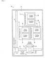
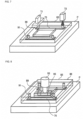
- Fig. 1 is a diagram illustrating a configuration of electronic device manufacturing apparatus (hereinafter, simply referred to as a "manufacturing apparatus" in some cases) 10 according to the present embodiment.
- Manufacturing apparatus 10 is provided with conveyance device 11, first shaping unit 13, second shaping unit 15, and component mounting unit 17.
- units 13, 15, and 17 and so on are arranged on base 19.
- Base 19 has a substantially rectangular shape in a plan view.
- a longitudinal direction of base 19 will be referred to as an X-axis direction
- a short direction of base 19 will be referred to as a Y-axis direction
- a direction that is orthogonal to both the X-axis direction and the Y-axis direction will be referred to as a Z-axis direction
- a direction of rotation about a straight line along the Z-axis direction will be referred to as a ⁇ -axis direction.
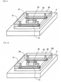
- Conveyance device 11 has X-axis slide mechanism 21 that extends in the X-axis direction and Y-axis slide mechanism 23 that extends in the Y-axis direction.
- X-axis slide mechanism 21 is held by base 19 and is disposed such that X-axis slider 25 can be moved in the X-axis direction.
- X-axis slider 25 of X-axis slide mechanism 21 is moved to any position in the X-axis direction due to the driving of electromagnetic motor 61 (refer to Fig. 2 ).
- One end section of Y-axis slide mechanism 23 in the Y-axis direction is held by X-axis slider 25 and Y-axis slide mechanism 23 is arranged such that stage 27 can be moved in the Y-axis direction.
- Stage 27 of Y-axis slide mechanism 23 is moved to any position in the Y-axis direction due to the driving of electromagnetic motor 63 (refer to Fig. 2 ). Accordingly, stage 27 can be moved to any position on base 19 by X-axis slide mechanism 21 and Y-axis slide mechanism 23 being driven.
- Stage 27 has base 31 and holding device 33.
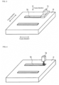
- Base 31 has the shape of a flat plate and shaping plate P (refer to Fig. 3 ) is placed on an upper face of base 31.
- Holding device 33 is arranged on both sides of base 31 in the X-axis direction.
- Stage 27 fixedly holds shaping plate P at a predetermined position by pinching an X-axis direction end section of shaping plate P placed on base 31 between base 31 and holding device 33.
- the X-axis direction and the Y-axis direction are directions that are orthogonal to each other and are parallel to a surface of base 31 on which shaping plate P is placed (one example of a placing surface).
- Conveyance device 11 also has lifting and lowering device 35 that lifts and lowers base 31 along with shaping plate P in the Z-axis direction.
- Lifting and lowering device 35 changes a position of shaping plate P in the Z-axis direction by lifting or lowering base 31 in due to the driving of driving section 65 (refer to Fig. 2 ).
- Driving section 65 is provided with, for example, an air cylinder as a driving source that lifts and lowers the base 31.
- lifting and lowering device 35 rotates base 31 in the ⁇ -axis direction due to to the driving of driving section 65.
- Driving section 65 is provided with, for example, an electromagnetic motor as a driving source that rotates base 31 in the ⁇ -axis direction. Together with stage 27, lifting and lowering device 35 is moved to any position on base 19.
- the three units 13, 15, and 17, that is, first shaping unit 13, second shaping unit 15, and component mounting unit 17, are arranged above base 19 (near side in the Z-axis direction in Fig. 1 ).
- Manufacturing apparatus 10 has a configuration that allows each of units 13, 15, and 17 to be attached to and detached from a connecting section (not illustrated) disposed at an upper portion of the apparatus.
- Manufacturing apparatus 10 is provided with, for example, multiple common connectors as connecting sections to which the respective units 13, 15, and 17 can be connected and a holding mechanism holding each of the units 13, 15, and 17 connected to the connectors. Accordingly, manufacturing apparatus 10 allows various units to be additionally installed or removed in accordance with the type of electronic device 100 to be manufactured (refer to Fig. 10 ) or the like.
- Units 13, 15, and 17 perform various works on shaping plate P from above stage 27 and shaping plate P, examples of the works including shaping of a three-dimensional article and mounting of electronic components 95 (refer to Fig. 10 ).
- First shaping unit 13 is a unit that shapes, for example, wiring pattern 75 and pillars 91 and 99 of electronic device 100 (refer to Fig. 10 ) and first shaping unit 13 is provided with first printing section 41 and firing section 43.
- First printing section 41 ejects a conductive material onto shaping plate P by, for example, driving inkjet head 71 (refer to Fig. 3 ).
- the conductive material is, for example, an ink that contains metal nanoparticles (such as silver) .
- Inkjet head 71 ejects the conductive material from multiple nozzles juxtaposed in the Y-axis direction by, for example, a piezo method using a piezoelectric element.
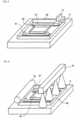
- Firing section 43 performs laser light emission from an emitting section 73 (refer to Fig. 4 ) and firing on the conductive material ejected onto shaping plate P. Then, for example, once shaping plate P has been moved to a position below first printing section 41 as a result of a movement of stage 27, shaping unit 13 forms wiring pattern 75 and pillars 91 and 99 by firing the ejected conductive material with emitting section 73 while ejecting the conductive material onto shaping plate P with inkjet head 71.
- Second shaping unit 15 is a unit that shapes, for example, insulating layer 85 (refer to Fig. 10 ) of electronic device 100 and second shaping unit 15 is provided with second printing section 45 and curing section 47.
- Second printing section 45 ejects a UV curable resin onto shaping plate P by, for example, driving inkjet head 77 (refer to Fig. 5 ).
- Inkjet head 77 may use, for example, a piezo method using a piezoelectric element or a thermal method based on ejection from a nozzle port of bubbles generated as a result of resin heating.
- Curing section 47 is provided with smoothing roller section 79 (refer to Fig. 6 ) that performs smoothing on an upper face of the UV curable resin ejected in the form of a single layer or predetermined multiple layers onto shaping plate P by inkjet head 77.
- Smoothing roller section 79 maintains a uniform thickness of each layer by, for example, smoothing a surface of the UV curable resin while scraping and collecting a surplus resin with a roller or a blade (not illustrated).
- Curing section 47 also has light emitting section 81 (refer to Fig. 6 ) that emits ultraviolet rays downward.
- Light emitting section 81 is provided with, for example, a mercury lamp or an LED as a light source.
- Curing section 47 performs the ultraviolet ray emission and curing on the UV curable resin ejected onto shaping plate P by driving light emitting section 81. Then, for example, once shaping plate P has been moved to a position below second printing section 45 as a result of a movement of stage 27, second shaping unit 15 shapes insulating layer 85 by curing the ejected UV curable resin with curing section 47 while ejecting the UV curable resin onto shaping plate P with inkjet head 77.
- Component mounting unit 17 is a unit that mounts various electronic components 95 (refer to Fig. 8 ) connected to pillar 91 shaped by first shaping unit 13, and component mounting unit 17 is provided with mounting section 48 and supply section 49.
- Mounting section 48 has a mounting head that holds electronic component 95 with suction nozzle 93 (refer to Fig. 8 ).
- mounting section 48 has a nozzle lifting and lowering device that lifts and lowers suction nozzle 93 and a nozzle rotation device that rotates suction nozzle 93 about an axial center; mounting section 48 is capable of changing a Z-axis direction position of electronic component 95 held by suction nozzle 93 and a posture in which electronic component 95 is held.
- Mounting section 48 may also be provided with a camera for confirming a mounting position by imaging wiring pattern 75, pillar 91, or the like, and a camera for imaging electronic component 95 and confirming the position of the component.
- Supply section 49 has, for example, multiple tape feeders, each of which feeds taped electronic components 95 one at a time, thus supplying electronic components 95 to mounting section 48.
- Supply section 49 is not limited to a tape feeder and may be a tray-type supply device wherein electronic components 95 are supplied and picked up from a tray.
- Supply section 49 may also be configured to be provided with both tape-type and tray-type supply devices or a supply device other than the tape-type and tray-type supply devices. For example, once shaping plate P has been moved to a position below mounting section 48 as a result of a movement of stage 27, component mounting unit 17 supplies a required component by driving supply section 49 and moving the mounting head of mounting section 48 to a component supply position of supply section 49.
- mounting section 48 mounts the electronic component 95 picked up from the supply position of supply section 49 by suction nozzle 93 of the mounting head at a position corresponding to, for example, a position where pillar 91 of a workpiece shaped on shaping plate P is shaped or is planned to be shaped.
- the three units 13, 15, and 17 described above are positioned on the same planes parallel to one another in the X-axis direction and the Y-axis direction with respective working positions of units 13, 15, and 17 fixed in the Z-axis direction.
- a nozzle port of inkjet head 71 of first shaping unit 13 and a nozzle port of inkjet head 77 of second shaping unit 15 share the same fixed position in the Z-axis direction.
- Z-axis-direction distances from stage 27 (three-dimensional article to be shaped) to inkjet heads 71 and 77 are equal to each other in a state where stage 27 does not move in the Z-axis direction.
- a position (working position) at a time when a droplet of the conductive material ejected from inkjet head 71 reaches the workpiece undergoing shaping on stage 27 is the same in the Z-axis direction as a position (working position) at a time when electronic component 95 held by the mounting head of mounting section 48 by the use of suction nozzle 93 is mounted on the workpiece.
- the amount by which the stage 27 is adjusted in position with respect to the Z-axis direction is extremely small, or adjustment is not required at all, in the case of a movement of stage 27 between the respective units 13, 15, and 17.
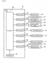
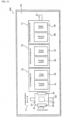
- control device 51 that controls the entire apparatus.
- Control device 51 is provided with controller 53 and multiple drive circuits 55.
- Controller 53 is provided with a CPU, a ROM, a RAM, and so on, has a computer as its main component, and is connected to the multiple drive circuits 55.
- Control device 51 also has storage device 57, in which control data is stored for conveyance device 11 and each of the units 13, 15, and 17 to be controlled in accordance with a work process regarding electronic device 100 to be manufactured.
- Storage device 57 is, for example, an optical drive device such as a hard disk device.
- the control data stored in storage device 57 is, for example, data including shaping data regarding sectional shapes of multiple layers obtained by insulating layer 85 of electronic device 100 being sliced to be given a predetermined thickness, and positional information (such as a recipe) for mounting electronic component 95 on shaped insulating layer 85.
- the multiple drive circuits 55 are respectively connected to the above-described holding device 33, electromagnetic motors 61 and 63, driving section 65, units 13, 15, and 17, and the like. Controller 53 controls operations of holding device 33 and so on via drive circuits 55 based on, for example, the control data in storage device 57. Controller 53 sequentially moves stage 27 to the working position of first shaping unit 13, second shaping unit 15, or component mounting unit 17 in accordance with the work process based on the control data for the manufacturing of electronic device 100 on shaping plate P.
- manufacturing apparatus 10 shapes, for example, multilayer wiring board 86 in which wiring pattern 75 and pillars 91 and 99 connected to electronic component 95 embedded in insulating layer 85 are formed as illustrated in Fig. 10 by sequentially stacking, onto shaping plate P, layers configuring multilayer wiring board 86 to be formed of multiple layers.
- controller 53 of control device 51 first controls X-axis slide mechanism 21 and Y-axis slide mechanism 23, carries stage 27 (refer to Fig. 1 ) where shaping plate P illustrated in Fig. 3 is set into first shaping unit 13, and moves it to a portion below inkjet head 71, which is a working position of first printing section 41.
- Controller 53 controls first shaping unit 13 based on the shaping data regarding the sectional shape of the first layer stored in storage device 57 and ejects conductive material onto shaping plate P from inkjet head 71.
- a film of the conductive material formed by multiple droplets is formed on shaping plate P.
- controller 53 controls firing section 43 and performs local heating and firing by emitting laser light from emitting section 73 to the film of the conductive material ejected by inkjet head 71 as illustrated in Fig. 4 .
- the sectional shape of the first layer is shaped on shaping plate P.
- Examples of a laser light source for firing section 43 include a semiconductor laser, a carbon dioxide laser, and a YAG laser.
- Controller 53 may perform the firing on the multiple layers all at once by the use of emitting section 73 with the multiple layers printed in advanced by inkjet head 71. Controller 53 may shape the desired wiring pattern 75 on shaping plate P by conducting the works that are illustrated in Fig. 3 and Fig. 4 once or multiple times. In addition, controller 53 may conduct the ejection by inkjet head 71 in parallel with the heating process by emitting section 73 (refer to Fig. 7 ) .
- controller 53 may conduct the work of first shaping unit 13 while moving both shaping plate P and stage 27 in the X-axis direction, the Y-axis direction, and the Z-axis direction as illustrated in Fig. 3 . Because stage 27 is moved as a main component in manufacturing apparatus 10 according to the present embodiment, inkjet head 71 and emitting section 73 of first shaping unit 13 can have fixed positions (in the X-axis direction and the like).
- controller 53 controls X-axis slide mechanism 21 and Y-axis slide mechanism 23, carries shaping plate P and stage 27 into second shaping unit 15, and moves shaping plate P and stage 27 to a portion below inkjet head 77, which is a working position of second printing section 45, as illustrated in Fig. 5 .
- Controller 53 controls second shaping unit 15 based on the shaping data stored in storage device 57 and ejects an insulating material onto shaping plate P from inkjet head 77.
- the insulating material is, for example, UV curable resin.
- controller 53 controls curing section 47 and performs smoothing, by the use of smoothing roller section 79, on the surface of a film of the stratified UV curable resin formed on shaping plate P as illustrated in Fig. 6 .
- Smoothing roller section 79 performs the smoothing of the surface of the workpiece and collection of the surplus UV curable resin by stage 27 moving in the X-axis direction in a state where, for example, smoothing roller section 79 is pressed against the surface of the layered workpiece (three-dimensional article) .
- First shaping unit 13 may also be provided with smoothing roller section 79, as in the case of second shaping unit 15, and the smoothing may also be conducted during the shaping of wiring pattern 75.
- controller 53 controls curing section 47 and performs the ultraviolet ray emission from light emitting section 81 and curing on the UV curable resin ejected by inkjet head 77. Controller 53 may also execute the curing process in parallel with the smoothing process by simultaneously driving smoothing roller section 79 and light emitting section 81.
- Ssecond shaping unit 15 repeatedly executes a series of processes consisting of the ejection by inkjet head 77, the smoothing by smoothing roller section 79, and the curing by light emitting section 81, and thereby shapes insulating layer 85 on wiring pattern 75.
- Through-hole 87 is shaped in insulating layer 85 in alignment with the position of wiring pattern 75 for pillar 91 (refer to Fig. 7 ) to be formed.
- Recessed portion 89 for the embedding of electronic component 95 is shaped in a substantially central portion of insulating layer 85 as well.
- Methods for forming through-hole 87 and recessed portion 89 are not limited to a formation method by which a position of the UV curable resin ejection from inkjet head 77 is adjusted based on the shaping data.
- through-hole 87 and the like may be formed by a part of insulating layer 85 being removed by means of laser light emission or the like after insulating layer 85 is formed in the shape of a flat plate.
- Through-hole 87 and the like may be formed by a support material being used as well.
- the support material mentioned in the previous sentence is, for example, a mold that is used for a three-dimensional article having a desired shape to be shaped and is removed after the shaping of the three-dimensional article.
- materials that can be dissolved in certain liquids such as water and chemicals can be used as the support material.
- controller 53 carries stage 27 back into first shaping unit 13 as illustrated in Fig. 7 .
- Controller 53 controls first shaping unit 13 and ejects the conductive material into through-hole 87 from inkjet head 71.
- controller 53 controls firing section 43 and performs the laser light emission from emitting section 73 and firing on the conductive material in through-hole 87.
- Controller 53 conducts the heating process by emitting section 73 in parallel with, for example, the ejection by inkjet head 77.
- Controller 53 repeatedly executes the ejection by inkjet head 71 and the firing by emitting section 73.
- Pillar 91 connected to wiring pattern 75 is shaped in the Z-axis direction through insulating layer 85.
- controller 53 controls first shaping unit 13 and second shaping unit 15, repeatedly executes the above-described processes that are illustrated in Figs. 3 to 7 , and shapes, for example, multilayer wiring board 86 (three-dimensional article) in which insulating layer 85, in which wiring pattern 75 and pillar 91 illustrated in Fig. 8 are formed, is stacked.
- controller 53 carries stage 27 into component mounting unit 17.
- controller 53 mounts electronic component 95 inside recessed portion 89 by controlling component mounting unit 17 after electronic component 95 is supplied from supply section 49 of mounting section 48 to suction nozzle 93 of mounting head.
- Negative pressure air or positive pressure air is supplied to suction nozzle 93 from, for example, a positive and negative pressure supply device (not illustrated).
- Suction nozzle 93 has a structure that picks up and holds the electronic component 95 using negative pressure and releases the held electronic component 95 by a slight positive pressure being supplied.
- Controller 53 adjusts the position of suction nozzle 93, the direction of electronic component 95, and the like by controlling component mounting unit 17 and mounts electronic component 95 inside recessed portion 89.
- stage 27 that is illustrated in Fig. 1 is provided with lifting and lowering device 35 that rotates base 31 in the ⁇ -axis direction. Accordingly, in manufacturing apparatus 10, the nozzle rotation device or the like may not be disposed in suction nozzle 93 in a case where the direction of electronic component 95 with respect to the multilayer wiring board 86 or the like is adjusted based on the rotation of stage 27 (shaping plate P) by lifting and lowering device 35.
- controller 53 carries stage 27 back into second shaping unit 15.
- Controller 53 controls second shaping unit 15, repeatedly executes a series of processes consisting of the UV curable resin ejection by inkjet head 77, the smoothing by smoothing roller section 79, and the curing of the UV curable resin by light emitting section 81, and embeds electronic component 95 inside recessed portion 89.
- through-hole 97 is formed in multilayer wiring board 86 in alignment with a position of a connection terminal of electronic component 95.
- controller 53 carries stage 27 back into first shaping unit 13. Controller 53 controls first shaping unit 13 based on the shaping data and ejects the conductive material into through-hole 97 from inkjet head 71. In addition, controller 53 controls firing section 43 and performs the laser light emission from emitting section 73 and firing on the conductive material in through-hole 97. Controller 53 repeatedly executes the ejection by inkjet head 71 and the firing by the emitting section 73. As illustrated in Fig. 10 , pillar 99 connected to the connection terminal of electronic component 95 is shaped in the Z-axis direction through multilayer wiring board 86. In this manner, manufacturing apparatus 10 is capable of manufacturing electronic device 100 on shaping plate P by using the respective units 13, 15, and 17.
- control device 51 controls conveyance device 11 and each of the units 13, 15, and 17 for each work process based on the control data stored in storage device 57.
- the arrangement of each of the units 13, 15, and 17 is determined in manufacturing apparatus 10 such that a path length of stage 27 that moves in accordance with a progress of the work process is minimized.
- Fig. 11 is a diagram illustrating an example of a movement path of stage 27 during the manufacturing of electronic device 100. According to movement path 110 that is illustrated in the upper section of Fig. 11 , the work in component mounting unit 17 is conducted after the work in first shaping unit 13 is completed, and then the work in the second shaping unit 15 is conducted last.
- Second shaping unit 15 is rotated by 180 degrees about a straight line along the Z-axis direction.
- each of the units 13, 15, and 17 is configured to be capable of being attached to and detached from an apparatus main body, and thus the direction of second shaping unit 15 can be changed by, for example, a user remounting second shaping unit 15 after removing it.
- Control device 51 needs to move stage 27 to the working position of second printing section 45 of second shaping unit 15 after the work in component mounting unit 17 has been conducted.
- movement path 110 curing section 47 is positioned between mounting section 48 of component mounting unit 17 and second printing section 45 of second shaping unit 15, and this results in an increase in distance.
- movement path 113 in contrast, the movement distance from mounting section 48 to second printing section 45 is shorter because second printing section 45 is arranged on the mounting section 48 side with respect to curing section 47.
- control device 51 determines the arrangement of each of the units 13, 15, and 17 before the execution of the work process varying with the type of electronic device 100 to be manufactured such that the path lengths of movement paths 110 and 113 along which stage 27 moves as a result of the execution of that work process are minimized. Then, for example, control device 51 displays the optimized arrangement of each of the units 13, 15, and 17 in a display section and notifies the user or the like of the optimized arrangement of each of the units 13, 15, and 17.
- conveyance device 11 is an example of a driving device.
- First shaping unit 13 and second shaping unit 15 are examples of a shaping unit.
- Component mounting unit 17 is an example of a mounting unit.
- Control device 51 is an example of a control section.
- Inkjet heads 71 and 77 are examples of an ejecting section.
- Electronic device 100 is an example of an electrical device.
- the X-axis direction and the Y-axis direction are examples of first and second directions.
- the Z-axis direction is an example of a third direction.
- conveyance device 11 is configured to be capable of moving stage 27 in four axial directions (in each of the X, Y, Z, and ⁇ directions)
- conveyance device 11 may be configured to be capable of moving stage 27 in only two directions, one being the X-axis direction and the other one being the Y-axis direction.
- lifting and lowering device 35 that moves stage 27 in the Z-axis direction and the ⁇ -axis direction can be omitted.
- each of the units 13, 15, and 17 may be configured for the respective working positions of the units 13, 15, and 17 to be variable in the Z-axis direction.
- each of the units 13, 15, and 17 is merely an example and can be appropriately changed.
- a configuration may be adopted in which the respective units 13, 15, and 17 are arranged on the same straight line along the X-axis direction as in manufacturing apparatus 10A illustrated in Fig. 12 .
- Y-axis slide mechanism 23 for moving stage 27 in the Y-axis direction can be omitted by, for example, a positional adjustment being performed with respect to the Y-axis direction on the side of each of the units 13, 15, and 17 (such as inkjet head 71).
- conveyance device 11 can be simplified in the form of a configuration made up of only X-axis slide mechanism 21 that moves stage 27 in the X-axis direction.
- the respective working positions of the units 13, 15, and 17 may be different positions in the Z-axis direction instead of the working positions aligned on the same planes.
- manufacturing apparatus 10 is provided with two shaping units 13 and 15, a configuration may be adopted instead in which only one shaping unit is provided.
- Manufacturing apparatus 10 according to the embodiment described above may also be configured to be provided with a unit other than the three units 13, 15, and 17 that has a different function.
- manufacturing apparatus 10B illustrated in Fig. 13 is provided with embedding unit 121 and adhesive application unit 131 in addition to the three units 13, 15, and 17.
- each of the units 13, 15, 17, 121, and 131 is arranged on a circumference about a connecting part (initial position of stage 27) between X-axis slide mechanism 21 and Y-axis slide mechanism 23.
- Embedding unit 121 is, for example, a unit for filling a relatively large hole or the like similar to recessed portion 89 according to the first embodiment with UV curable resin, and embedding unit 121 is provided with first application section 123 and first curing section 125.
- First application section 123 has, for example, a dispenser that provides an ejection amount greater than that of inkjet head 77 of second printing section 45.
- First curing section 125 has a light source (such as a mercury lamp and an LED) that emits more light than light emitting section 81 of curing section 47.
- Adhesive application unit 131 which is a unit for adhesion and fixing of electronic component 95 or the like to insulating layer 85, is provided with second application section 133 and second curing section 135.
- Second application section 133 applies, for example, a UV curing adhesive to an upper face of insulating layer 85 where electronic component 95 is arranged.
- the type of the adhesive is not particularly limited, it is preferable that the adhesive is selected based on, for example, a heat shrinkage factor and an adhesive strength in accordance with the material of the three-dimensional article (insulating layer 85 and electronic component 95).
- Second curing section 135 causes electronic component 95 to adhere to the insulating layer 85 by applying the adhesive with ultraviolet rays.
- manufacturing apparatus 10B that has the configuration illustrated in Fig. 13 is effective.
- the functions of the units added to manufacturing apparatus 10B are merely examples.
- the present invention is not limited thereto and manufacturing apparatus 10B may also be provided with, for example, a solder application and firing unit.
- the additive manufacturing for multilayer wiring board 86 is not limited to droplet ejection such as inkjetting and it may be replaced with a shaping method employing powder material spreading and binder-based powder material coupling. Alternatively, it may be replaced with a shaping method employing powder material spreading and sintering based on application of laser light.
- a shaping method employing powder material spreading and sintering based on application of laser light may be replaced with each of the units 13, 15, and 17 according to the embodiment described above.
- the units 13, 15, and 17 may also be integrated with the apparatus main body not to be capable of being removed instead.
Landscapes
- Engineering & Computer Science (AREA)
- Manufacturing & Machinery (AREA)
- Microelectronics & Electronic Packaging (AREA)
- Chemical & Material Sciences (AREA)
- Mechanical Engineering (AREA)
- Materials Engineering (AREA)
- Optics & Photonics (AREA)
- Nanotechnology (AREA)
- Dispersion Chemistry (AREA)
- Physics & Mathematics (AREA)
- Manufacturing Of Printed Wiring (AREA)
- Powder Metallurgy (AREA)
- Production Of Multi-Layered Print Wiring Board (AREA)
Claims (8)
- Appareil de fabrication (10) comprenant :une platine (27) comprenant une surface de placement où un article tridimensionnel est placé ;un dispositif d'entraînement (11) qui déplace la platine (27) dans une première direction et une deuxième direction, la première direction et la deuxième direction étant des directions parallèles à la surface de placement et différentes l'une de l'autre ;une unité de mise en forme (13, 15) qui est disposée dans une plage où la platine (27) peut être déplacée et forme chaque couche de l'article tridimensionnel à former par des couches multiples ;une unité de montage (17) qui est disposée dans la plage où la platine (27) peut être déplacée et monte un composant électronique (95) sur une pièce stratifiée formée par l'unité de mise en forme (13, 15) ; etune section de contrôle (51) qui déplace séquentiellement la platine (27) jusqu'à une position de travail soit de l'unité de mise en forme (13, 15), soit de l'unité de montage (17), selon un chemin déterminé sur la base d'un processus de travail pour mettre en œuvre une fabrication additive d'un dispositif électrique (100) sur la platine (27),l'appareil de fabrication est caractérisé en ce que :
la première direction et la deuxième direction sont des directions orthogonales entre elles. - Appareil de fabrication (10) selon la revendication 1,
dans lequel le dispositif d'entraînement (11) est configuré pour être capable de déplacer la platine (27) dans une troisième direction ainsi que dans les première et deuxième directions, la troisième direction étant orthogonale à la surface de placement. - Appareil de fabrication (10) selon la revendication 2,
dans lequel l'unité de mise en forme (13, 15) et l'unité de montage (17) sont dans un état où les positions de travail par rapport à la troisième direction sont fixes et les positions de travail sont positionnées dans le même plan. - Appareil de fabrication (10) selon l'une quelconque des revendications 1 à 3,
dans lequel l'unité de mise en forme (13, 15) comprend une section d'éjection qui éjecte un matériau liquide sur la platine (27) par éjection de gouttelettes. - Appareil de fabrication (10) selon la revendication 4,dans lequel l'article tridimensionnel est une carte de câblage multicouche, etdans lequel de multiples unités de mise en forme (13, 15) sont pourvues, les deux ou plusieurs unités de mise en forme (13, 15) comprenant au moins une unité de mise en forme (13, 15) qui met en forme un schéma de câblage par le tir d'un matériau conducteur éjecté sur la platine (27) par la section d'éjection, et une unité de mise en forme (13, 15) qui met en forme une couche isolante en durcissant un matériau isolant éjecté sur la platine (27) par la section d'éjection.
- Appareil de fabrication (10) selon l'une quelconque des revendications 1 à 5,
dans lequel l'unité de mise en forme (13, 15) et l'unité de montage (17) sont configurées pour pouvoir être attachées à un corps principal de l'appareil de fabrication (10) et détachées de celui-ci. - Appareil de fabrication (10) selon la revendication 6,
dans lequel la section de contrôle (51) détermine l'agencement de l'unité de mise en forme (13, 15) et de l'unité de montage (17) par rapport à une direction de déplacement de la platine (27) sur la base du processus de travail de telle sorte que le chemin de déplacement de la platine (27) est minimisé en longueur. - Procédé de fabrication comprenant :la commande d'un appareil de fabrication (10) comprenant une platine (27) ayant une surface de placement où un article tridimensionnel est placé, d'un dispositif d'entraînement (11) qui déplace la platine (27) dans une première direction et une deuxième direction, la première direction et la deuxième direction étant des directions parallèles à la surface de placement et différentes l'une de l'autre, d'une unité de mise en forme (13, 15) qui est disposée dans une plage où la platine (27) peut être déplacée et forme chaque couche de l'article tridimensionnel à former par des couches multiples, et d'une unité de montage (17) qui est disposée dans la plage où la platine (27) peut être déplacée et monte un composant électronique (95) sur une pièce stratifiée formée par l'unité de mise en forme (13, 15), pour déplacer séquentiellement la platine (27) jusqu'à une position de travail soit de l'unité de mise en forme (13, 15), soit de l'unité de montage (17), selon un chemin déterminé sur la base d'un processus de travail, et pour mettre en œuvre la fabrication additive d'un dispositif électrique (100) sur la platine (27),caractérisé en ce que : la première direction et la deuxième direction sont des directions orthogonales entre elles.
Applications Claiming Priority (1)
| Application Number | Priority Date | Filing Date | Title |
|---|---|---|---|
| PCT/JP2014/074829 WO2016042657A1 (fr) | 2014-09-19 | 2014-09-19 | Appareil de fabrication et procédé de fabrication |
Publications (4)
| Publication Number | Publication Date |
|---|---|
| EP3219467A1 EP3219467A1 (fr) | 2017-09-20 |
| EP3219467A4 EP3219467A4 (fr) | 2018-05-23 |
| EP3219467B1 EP3219467B1 (fr) | 2020-09-16 |
| EP3219467B2 true EP3219467B2 (fr) | 2023-08-16 |
Family
ID=55532720
Family Applications (1)
| Application Number | Title | Priority Date | Filing Date |
|---|---|---|---|
| EP14902233.7A Active EP3219467B2 (fr) | 2014-09-19 | 2014-09-19 | Appareil de fabrication et procédé de fabrication |
Country Status (5)
| Country | Link |
|---|---|
| US (2) | US10667403B2 (fr) |
| EP (1) | EP3219467B2 (fr) |
| JP (1) | JP6403785B2 (fr) |
| CN (1) | CN107073817A (fr) |
| WO (1) | WO2016042657A1 (fr) |
Families Citing this family (21)
| Publication number | Priority date | Publication date | Assignee | Title |
|---|---|---|---|---|
| DE102016104677A1 (de) * | 2016-03-14 | 2017-09-14 | Cl Schutzrechtsverwaltungs Gmbh | Anlage zur additiven Herstellung dreidimensionaler Objekte |
| CN109314086B (zh) * | 2016-06-08 | 2022-11-04 | 株式会社富士 | 电路形成方法 |
| WO2018140517A1 (fr) * | 2017-01-26 | 2018-08-02 | Nano-Dimension Technologies, Ltd. | Cartes de circuit imprimé à puces intégrées et procédés de fabrication |
| JP6907657B2 (ja) | 2017-03-31 | 2021-07-21 | セイコーエプソン株式会社 | 三次元造形物の製造方法 |
| EP3716741A4 (fr) | 2017-11-21 | 2020-11-18 | Fuji Corporation | Procédé de production de dispositif électronique multicouche tridimensionnel, et dispositif électronique multicouche tridimensionnel |
| JP6909870B2 (ja) * | 2017-12-06 | 2021-07-28 | 株式会社Fuji | 支持部材の形成方法、及び構造物の形成方法 |
| US20210060850A1 (en) * | 2017-12-31 | 2021-03-04 | Stratasys Ltd. | 3d printing to obtain a predefined surface quality |
| JP6909920B2 (ja) * | 2018-03-08 | 2021-07-28 | 株式会社Fuji | 情報処理装置 |
| CN108538755B (zh) * | 2018-03-22 | 2019-05-21 | 华中科技大学 | 一种复杂曲面电子系统的共形制造设备及方法 |
| CN108419374A (zh) * | 2018-05-18 | 2018-08-17 | 湖州旭源电气科技有限公司 | 一种pcb板自动加工设备 |
| JP7114147B2 (ja) * | 2018-10-02 | 2022-08-08 | エルジー・ケム・リミテッド | 成形装置及び成形体の製造方法 |
| DE102018125216B3 (de) * | 2018-10-11 | 2020-02-06 | Neotech AMT GmbH | Verfahren zur Vorbereitung der automatisierten Herstellung einer Elektronikkomponente, Verfahren zur automatisierten Herstellung und/oder zum automatisierten Nachbearbeiten einer Elektronikkomponente, Recheneinrichtung, Computerprogramm und elektronisch lesbarer Datenträger |
| DE102019202245A1 (de) * | 2019-02-19 | 2020-08-20 | Ekra Automatisierungssysteme Gmbh | Druckeinrichtung und Verfahren |
| JP2020136640A (ja) * | 2019-02-26 | 2020-08-31 | トヨタ自動車株式会社 | 膜の製造方法 |
| JP7120120B2 (ja) * | 2019-03-29 | 2022-08-17 | 新東工業株式会社 | 付加製造装置及び付加製造方法 |
| CN110182756B (zh) * | 2019-06-04 | 2023-02-21 | 百色学院 | 一种多环节可见光的光驱微纳马达的制备方法 |
| US20220354000A1 (en) * | 2019-06-18 | 2022-11-03 | Fuji Corporation | Circuit board manufacturing method and circuit board manufacturing device |
| EP4002962A4 (fr) * | 2019-07-16 | 2022-07-20 | Fuji Corporation | Machine de moulage tridimensionnel et machine de montage de composant |
| US20220279658A1 (en) * | 2019-07-31 | 2022-09-01 | Fuji Corporation | Method for manufacturing circuit wiring by three-dimensional additive manufacturing |
| KR102416785B1 (ko) * | 2020-11-12 | 2022-07-05 | 주식회사 덴티스 | 3차원 프린터 및 이의 구동 방법 |
| CN113618081B (zh) * | 2021-08-17 | 2023-09-26 | 温州大学 | 一种可选热源增材轧制一体成型装置 |
Family Cites Families (39)
| Publication number | Priority date | Publication date | Assignee | Title |
|---|---|---|---|---|
| JPH0730362B2 (ja) * | 1987-03-20 | 1995-04-05 | 株式会社日立製作所 | 電子部品及びその製造方法 |
| US5594652A (en) * | 1991-01-31 | 1997-01-14 | Texas Instruments Incorporated | Method and apparatus for the computer-controlled manufacture of three-dimensional objects from computer data |
| JPH04268790A (ja) * | 1991-02-25 | 1992-09-24 | Yamatake Honeywell Co Ltd | 回路基板製造方法及び装置 |
| JPH1041695A (ja) * | 1996-07-24 | 1998-02-13 | Matsushita Electric Ind Co Ltd | チップ部品装着装置 |
| US5783008A (en) * | 1997-03-31 | 1998-07-21 | Ford Global Technologies, Inc. | Apparatus and method for embedding conductors in a non-planar substrate |
| IL121458A0 (en) * | 1997-08-03 | 1998-02-08 | Lipsker Daniel | Rapid prototyping |
| JP4741045B2 (ja) * | 1998-03-25 | 2011-08-03 | セイコーエプソン株式会社 | 電気回路、その製造方法および電気回路製造装置 |
| JP2000141497A (ja) * | 1998-11-09 | 2000-05-23 | Sanyo Electric Co Ltd | 立体配線装置及びその方法 |
| JP4128292B2 (ja) * | 1999-01-14 | 2008-07-30 | 幸士 生田 | 光造形加工法および該加工法により製作される装置 |
| EP1203662B1 (fr) * | 1999-07-26 | 2010-12-15 | Panasonic Corporation | Dispositif d'impression a soudure en pate et son procede d'impression |
| US6463349B2 (en) * | 2000-03-23 | 2002-10-08 | Solidica, Inc. | Ultrasonic object consolidation system and method |
| US20020147521A1 (en) * | 2001-03-14 | 2002-10-10 | Milling Systems And Concepts Pte Ltd. | Prototype production system and method |
| JP4228677B2 (ja) * | 2002-12-06 | 2009-02-25 | パナソニック株式会社 | 回路基板 |
| US20040151978A1 (en) * | 2003-01-30 | 2004-08-05 | Huang Wen C. | Method and apparatus for direct-write of functional materials with a controlled orientation |
| US7556490B2 (en) * | 2004-07-30 | 2009-07-07 | Board Of Regents, The University Of Texas System | Multi-material stereolithography |
| US9723866B2 (en) * | 2004-08-11 | 2017-08-08 | Cornell University | System and method for solid freeform fabrication of edible food |
| JP4052295B2 (ja) * | 2004-08-25 | 2008-02-27 | セイコーエプソン株式会社 | 多層配線基板の製造方法、電子デバイス及び電子機器 |
| US7658603B2 (en) * | 2005-03-31 | 2010-02-09 | Board Of Regents, The University Of Texas System | Methods and systems for integrating fluid dispensing technology with stereolithography |
| US20070248798A1 (en) * | 2006-04-19 | 2007-10-25 | Canon Kabushiki Kaisha | Circuit board manufacturing process, circuit board manufactured by the process, and circuit board manufacturing apparatus |
| US7952888B2 (en) * | 2006-05-09 | 2011-05-31 | Canon Kabushiki Kaisha | Wiring module |
| DE102006037927A1 (de) | 2006-08-11 | 2008-02-14 | Karl Hehl | Verfahren und Vorrichtung zur Herstellung eines dreidimensionalen Gegenstandes sowie Verwendung einer kunststofftechnischen Einheit zu dessen Herstellung |
| WO2008102266A2 (fr) * | 2007-02-23 | 2008-08-28 | Infermata Systems Ltd. | Procédé et appareil pour la fabrication rapide d'une carte de circuits imprimés fonctionnelle |
| US20090255426A1 (en) * | 2008-02-14 | 2009-10-15 | Illinois Tool Works Inc. | Method and apparatus for placing substrate support components |
| US7880489B2 (en) | 2008-11-04 | 2011-02-01 | Formfactor, Inc. | Printing of redistribution traces on electronic component |
| US20100291304A1 (en) * | 2009-02-24 | 2010-11-18 | Tracy Becker | Multifunctional Manufacturing Platform And Method Of Using The Same |
| JP2011241450A (ja) | 2010-05-19 | 2011-12-01 | Keijiro Yamamoto | 積層造形方法及び積層造形装置 |
| DE102010044268A1 (de) | 2010-09-02 | 2012-03-08 | Arburg Gmbh + Co Kg | Verfahren und Vorrichtung zur Herstellung eines dreidimensionalen Gegenstandes |
| EP2731783A4 (fr) * | 2011-07-13 | 2016-03-09 | Nuvotronics Llc | Procédés de fabrication de structures électroniques et mécaniques |
| US10748867B2 (en) * | 2012-01-04 | 2020-08-18 | Board Of Regents, The University Of Texas System | Extrusion-based additive manufacturing system for 3D structural electronic, electromagnetic and electromechanical components/devices |
| US10518490B2 (en) * | 2013-03-14 | 2019-12-31 | Board Of Regents, The University Of Texas System | Methods and systems for embedding filaments in 3D structures, structural components, and structural electronic, electromagnetic and electromechanical components/devices |
| JP2013258172A (ja) | 2012-06-11 | 2013-12-26 | Panasonic Corp | 電子部品実装システムおよび電子部品実装方法 |
| EP3013565B1 (fr) * | 2013-06-24 | 2020-01-22 | President and Fellows of Harvard College | Pièce fonctionnelle imprimée en trois dimensions (3d) et procédé de réalisation |
| CN103327741B (zh) * | 2013-07-04 | 2016-03-02 | 江俊逢 | 一种基于3d打印的封装基板及其制造方法 |
| US9545756B2 (en) * | 2013-09-29 | 2017-01-17 | Makerbot Industries, Llc | Purge wall for three-dimensional printing |
| DE102013220578A1 (de) | 2013-10-11 | 2015-04-16 | Arburg Gmbh + Co. Kg | Dreidimensionaler Gegenstand mit selbsttragend hergestellter Wandung |
| US20150197062A1 (en) * | 2014-01-12 | 2015-07-16 | Zohar SHINAR | Method, device, and system of three-dimensional printing |
| US20150201500A1 (en) * | 2014-01-12 | 2015-07-16 | Zohar SHINAR | System, device, and method of three-dimensional printing |
| EP3134253A4 (fr) * | 2014-04-21 | 2018-06-13 | Cornell University | Système et procédés de fabrication additive d'ensembles électromécaniques |
| US9764515B2 (en) * | 2014-05-01 | 2017-09-19 | Musc Foundation For Research Development | Multidispensor cartesian robotic printer |
-
2014
- 2014-09-19 US US15/512,101 patent/US10667403B2/en active Active
- 2014-09-19 EP EP14902233.7A patent/EP3219467B2/fr active Active
- 2014-09-19 CN CN201480081908.8A patent/CN107073817A/zh active Pending
- 2014-09-19 JP JP2016548507A patent/JP6403785B2/ja active Active
- 2014-09-19 WO PCT/JP2014/074829 patent/WO2016042657A1/fr active Application Filing
-
2019
- 2019-11-19 US US16/688,579 patent/US11470724B2/en active Active
Also Published As
| Publication number | Publication date |
|---|---|
| US20200093000A1 (en) | 2020-03-19 |
| US10667403B2 (en) | 2020-05-26 |
| WO2016042657A1 (fr) | 2016-03-24 |
| US20170280567A1 (en) | 2017-09-28 |
| JP6403785B2 (ja) | 2018-10-10 |
| JPWO2016042657A1 (ja) | 2017-07-06 |
| CN107073817A (zh) | 2017-08-18 |
| EP3219467A4 (fr) | 2018-05-23 |
| EP3219467B1 (fr) | 2020-09-16 |
| EP3219467A1 (fr) | 2017-09-20 |
| US11470724B2 (en) | 2022-10-11 |
Similar Documents
| Publication | Publication Date | Title |
|---|---|---|
| US11470724B2 (en) | Manufacturing apparatus for performing additive manufacturing of an electrical device | |
| US11458722B2 (en) | Three-dimensional multi-layer electronic device production method | |
| EP3254833B1 (fr) | Système de fabrication additive | |
| WO2016147284A1 (fr) | Procédé de formation et dispositif de formation | |
| JP7316742B2 (ja) | 3次元積層造形による実装基板の製造方法 | |
| US20210267054A1 (en) | Circuit formation method and circuit formation device | |
| JP6714109B2 (ja) | 回路形成方法、および回路形成装置 | |
| JP2017028053A (ja) | 回路形成方法 | |
| EP4000930A1 (fr) | Machine de moulage en trois dimensions | |
| JPWO2017212567A1 (ja) | 回路形成方法 | |
| JP7394626B2 (ja) | 3次元積層電子デバイスの製造方法及び製造装置 | |
| JPH10112585A (ja) | プリント配線体及びその製造方法並びにその製造装置 | |
| WO2021075051A1 (fr) | Procédé de montage de composant et dispositif de montage de composant | |
| WO2019058497A1 (fr) | Procédé de formation de structure et procédé d'examen de structure | |
| JP7145334B2 (ja) | 3次元積層造形による電子回路製造方法 | |
| WO2019111347A1 (fr) | Procédé pour la formation d'un élément de support et procédé pour la formation d'une structure | |
| JP7238206B2 (ja) | 造形方法 | |
| WO2023223562A1 (fr) | Procédé de fabrication et dispositif de fabrication | |
| WO2023079607A1 (fr) | Procédé de formation de circuit et appareil de formation de circuit | |
| JP7358614B2 (ja) | 配線形成方法 | |
| JP7284275B2 (ja) | 3次元積層造形による3次元積層電子デバイスの製造方法 | |
| EP4117397A1 (fr) | Procédé de formation de câblage | |
| JP7062795B2 (ja) | 回路形成装置 | |
| JP2022112234A (ja) | 3次元造形物製造装置及び表示方法 |
Legal Events
| Date | Code | Title | Description |
|---|---|---|---|
| STAA | Information on the status of an ep patent application or granted ep patent |
Free format text: STATUS: THE INTERNATIONAL PUBLICATION HAS BEEN MADE |
|
| PUAI | Public reference made under article 153(3) epc to a published international application that has entered the european phase |
Free format text: ORIGINAL CODE: 0009012 |
|
| STAA | Information on the status of an ep patent application or granted ep patent |
Free format text: STATUS: REQUEST FOR EXAMINATION WAS MADE |
|
| 17P | Request for examination filed |
Effective date: 20170217 |
|
| AK | Designated contracting states |
Kind code of ref document: A1 Designated state(s): AL AT BE BG CH CY CZ DE DK EE ES FI FR GB GR HR HU IE IS IT LI LT LU LV MC MK MT NL NO PL PT RO RS SE SI SK SM TR |
|
| AX | Request for extension of the european patent |
Extension state: BA ME |
|
| DAX | Request for extension of the european patent (deleted) | ||
| A4 | Supplementary search report drawn up and despatched |
Effective date: 20180424 |
|
| RIC1 | Information provided on ipc code assigned before grant |
Ipc: B29C 67/00 20170101AFI20180417BHEP Ipc: H05K 3/46 20060101ALI20180417BHEP Ipc: B22F 3/105 20060101ALI20180417BHEP Ipc: H05K 3/12 20060101ALI20180417BHEP Ipc: H05K 1/09 20060101ALI20180417BHEP |
|
| RAP1 | Party data changed (applicant data changed or rights of an application transferred) |
Owner name: FUJI CORPORATION |
|
| RIN1 | Information on inventor provided before grant (corrected) |
Inventor name: FUJITA, MASATOSHI Inventor name: KAWAJIRI, AKIHIRO Inventor name: TSUKADA, KENJI Inventor name: SUZUKI, MASATO Inventor name: HASHIMOTO, YOSHITAKA |
|
| REG | Reference to a national code |
Ref country code: DE Ref legal event code: R079 Ref document number: 602014070360 Country of ref document: DE Free format text: PREVIOUS MAIN CLASS: B29C0067000000 Ipc: B33Y0080000000 |
|
| GRAP | Despatch of communication of intention to grant a patent |
Free format text: ORIGINAL CODE: EPIDOSNIGR1 |
|
| STAA | Information on the status of an ep patent application or granted ep patent |
Free format text: STATUS: GRANT OF PATENT IS INTENDED |
|
| RIC1 | Information provided on ipc code assigned before grant |
Ipc: B29C 67/00 20170101ALI20200424BHEP Ipc: H05K 1/09 20060101ALI20200424BHEP Ipc: B33Y 80/00 20150101AFI20200424BHEP Ipc: H05K 3/12 20060101ALI20200424BHEP Ipc: B22F 3/105 20060101ALI20200424BHEP Ipc: H05K 3/46 20060101ALI20200424BHEP |
|
| INTG | Intention to grant announced |
Effective date: 20200526 |
|
| GRAS | Grant fee paid |
Free format text: ORIGINAL CODE: EPIDOSNIGR3 |
|
| GRAA | (expected) grant |
Free format text: ORIGINAL CODE: 0009210 |
|
| STAA | Information on the status of an ep patent application or granted ep patent |
Free format text: STATUS: THE PATENT HAS BEEN GRANTED |
|
| AK | Designated contracting states |
Kind code of ref document: B1 Designated state(s): AL AT BE BG CH CY CZ DE DK EE ES FI FR GB GR HR HU IE IS IT LI LT LU LV MC MK MT NL NO PL PT RO RS SE SI SK SM TR |
|
| REG | Reference to a national code |
Ref country code: GB Ref legal event code: FG4D |
|
| REG | Reference to a national code |
Ref country code: CH Ref legal event code: EP |
|
| REG | Reference to a national code |
Ref country code: DE Ref legal event code: R096 Ref document number: 602014070360 Country of ref document: DE |
|
| REG | Reference to a national code |
Ref country code: IE Ref legal event code: FG4D |
|
| REG | Reference to a national code |
Ref country code: AT Ref legal event code: REF Ref document number: 1313798 Country of ref document: AT Kind code of ref document: T Effective date: 20201015 |
|
| PG25 | Lapsed in a contracting state [announced via postgrant information from national office to epo] |
Ref country code: NO Free format text: LAPSE BECAUSE OF FAILURE TO SUBMIT A TRANSLATION OF THE DESCRIPTION OR TO PAY THE FEE WITHIN THE PRESCRIBED TIME-LIMIT Effective date: 20201216 Ref country code: GR Free format text: LAPSE BECAUSE OF FAILURE TO SUBMIT A TRANSLATION OF THE DESCRIPTION OR TO PAY THE FEE WITHIN THE PRESCRIBED TIME-LIMIT Effective date: 20201217 Ref country code: BG Free format text: LAPSE BECAUSE OF FAILURE TO SUBMIT A TRANSLATION OF THE DESCRIPTION OR TO PAY THE FEE WITHIN THE PRESCRIBED TIME-LIMIT Effective date: 20201216 Ref country code: FI Free format text: LAPSE BECAUSE OF FAILURE TO SUBMIT A TRANSLATION OF THE DESCRIPTION OR TO PAY THE FEE WITHIN THE PRESCRIBED TIME-LIMIT Effective date: 20200916 Ref country code: HR Free format text: LAPSE BECAUSE OF FAILURE TO SUBMIT A TRANSLATION OF THE DESCRIPTION OR TO PAY THE FEE WITHIN THE PRESCRIBED TIME-LIMIT Effective date: 20200916 Ref country code: SE Free format text: LAPSE BECAUSE OF FAILURE TO SUBMIT A TRANSLATION OF THE DESCRIPTION OR TO PAY THE FEE WITHIN THE PRESCRIBED TIME-LIMIT Effective date: 20200916 |
|
| REG | Reference to a national code |
Ref country code: AT Ref legal event code: MK05 Ref document number: 1313798 Country of ref document: AT Kind code of ref document: T Effective date: 20200916 |
|
| REG | Reference to a national code |
Ref country code: NL Ref legal event code: MP Effective date: 20200916 |
|
| PG25 | Lapsed in a contracting state [announced via postgrant information from national office to epo] |
Ref country code: LV Free format text: LAPSE BECAUSE OF FAILURE TO SUBMIT A TRANSLATION OF THE DESCRIPTION OR TO PAY THE FEE WITHIN THE PRESCRIBED TIME-LIMIT Effective date: 20200916 Ref country code: RS Free format text: LAPSE BECAUSE OF FAILURE TO SUBMIT A TRANSLATION OF THE DESCRIPTION OR TO PAY THE FEE WITHIN THE PRESCRIBED TIME-LIMIT Effective date: 20200916 |
|
| REG | Reference to a national code |
Ref country code: LT Ref legal event code: MG4D |
|
| PG25 | Lapsed in a contracting state [announced via postgrant information from national office to epo] |
Ref country code: CZ Free format text: LAPSE BECAUSE OF FAILURE TO SUBMIT A TRANSLATION OF THE DESCRIPTION OR TO PAY THE FEE WITHIN THE PRESCRIBED TIME-LIMIT Effective date: 20200916 Ref country code: RO Free format text: LAPSE BECAUSE OF FAILURE TO SUBMIT A TRANSLATION OF THE DESCRIPTION OR TO PAY THE FEE WITHIN THE PRESCRIBED TIME-LIMIT Effective date: 20200916 Ref country code: SM Free format text: LAPSE BECAUSE OF FAILURE TO SUBMIT A TRANSLATION OF THE DESCRIPTION OR TO PAY THE FEE WITHIN THE PRESCRIBED TIME-LIMIT Effective date: 20200916 Ref country code: EE Free format text: LAPSE BECAUSE OF FAILURE TO SUBMIT A TRANSLATION OF THE DESCRIPTION OR TO PAY THE FEE WITHIN THE PRESCRIBED TIME-LIMIT Effective date: 20200916 Ref country code: LT Free format text: LAPSE BECAUSE OF FAILURE TO SUBMIT A TRANSLATION OF THE DESCRIPTION OR TO PAY THE FEE WITHIN THE PRESCRIBED TIME-LIMIT Effective date: 20200916 Ref country code: PT Free format text: LAPSE BECAUSE OF FAILURE TO SUBMIT A TRANSLATION OF THE DESCRIPTION OR TO PAY THE FEE WITHIN THE PRESCRIBED TIME-LIMIT Effective date: 20210118 |
|
| REG | Reference to a national code |
Ref country code: CH Ref legal event code: PL |
|
| PG25 | Lapsed in a contracting state [announced via postgrant information from national office to epo] |
Ref country code: AL Free format text: LAPSE BECAUSE OF FAILURE TO SUBMIT A TRANSLATION OF THE DESCRIPTION OR TO PAY THE FEE WITHIN THE PRESCRIBED TIME-LIMIT Effective date: 20200916 Ref country code: AT Free format text: LAPSE BECAUSE OF FAILURE TO SUBMIT A TRANSLATION OF THE DESCRIPTION OR TO PAY THE FEE WITHIN THE PRESCRIBED TIME-LIMIT Effective date: 20200916 Ref country code: ES Free format text: LAPSE BECAUSE OF FAILURE TO SUBMIT A TRANSLATION OF THE DESCRIPTION OR TO PAY THE FEE WITHIN THE PRESCRIBED TIME-LIMIT Effective date: 20200916 Ref country code: IS Free format text: LAPSE BECAUSE OF FAILURE TO SUBMIT A TRANSLATION OF THE DESCRIPTION OR TO PAY THE FEE WITHIN THE PRESCRIBED TIME-LIMIT Effective date: 20210116 Ref country code: PL Free format text: LAPSE BECAUSE OF FAILURE TO SUBMIT A TRANSLATION OF THE DESCRIPTION OR TO PAY THE FEE WITHIN THE PRESCRIBED TIME-LIMIT Effective date: 20200916 |
|
| REG | Reference to a national code |
Ref country code: DE Ref legal event code: R026 Ref document number: 602014070360 Country of ref document: DE |
|
| PLBI | Opposition filed |
Free format text: ORIGINAL CODE: 0009260 |
|
| REG | Reference to a national code |
Ref country code: BE Ref legal event code: MM Effective date: 20200930 |
|
| PLAX | Notice of opposition and request to file observation + time limit sent |
Free format text: ORIGINAL CODE: EPIDOSNOBS2 |
|
| PG25 | Lapsed in a contracting state [announced via postgrant information from national office to epo] |
Ref country code: LU Free format text: LAPSE BECAUSE OF NON-PAYMENT OF DUE FEES Effective date: 20200919 Ref country code: MC Free format text: LAPSE BECAUSE OF FAILURE TO SUBMIT A TRANSLATION OF THE DESCRIPTION OR TO PAY THE FEE WITHIN THE PRESCRIBED TIME-LIMIT Effective date: 20200916 Ref country code: SK Free format text: LAPSE BECAUSE OF FAILURE TO SUBMIT A TRANSLATION OF THE DESCRIPTION OR TO PAY THE FEE WITHIN THE PRESCRIBED TIME-LIMIT Effective date: 20200916 |
|
| 26 | Opposition filed |
Opponent name: ARBURG GMBH + CO. KG Effective date: 20210611 |
|
| GBPC | Gb: european patent ceased through non-payment of renewal fee |
Effective date: 20201216 |
|
| PG25 | Lapsed in a contracting state [announced via postgrant information from national office to epo] |
Ref country code: SI Free format text: LAPSE BECAUSE OF FAILURE TO SUBMIT A TRANSLATION OF THE DESCRIPTION OR TO PAY THE FEE WITHIN THE PRESCRIBED TIME-LIMIT Effective date: 20200916 Ref country code: IE Free format text: LAPSE BECAUSE OF NON-PAYMENT OF DUE FEES Effective date: 20200919 Ref country code: LI Free format text: LAPSE BECAUSE OF NON-PAYMENT OF DUE FEES Effective date: 20200930 Ref country code: BE Free format text: LAPSE BECAUSE OF NON-PAYMENT OF DUE FEES Effective date: 20200930 Ref country code: CH Free format text: LAPSE BECAUSE OF NON-PAYMENT OF DUE FEES Effective date: 20200930 Ref country code: DK Free format text: LAPSE BECAUSE OF FAILURE TO SUBMIT A TRANSLATION OF THE DESCRIPTION OR TO PAY THE FEE WITHIN THE PRESCRIBED TIME-LIMIT Effective date: 20200916 |
|
| PLBB | Reply of patent proprietor to notice(s) of opposition received |
Free format text: ORIGINAL CODE: EPIDOSNOBS3 |
|
| PG25 | Lapsed in a contracting state [announced via postgrant information from national office to epo] |
Ref country code: FR Free format text: LAPSE BECAUSE OF NON-PAYMENT OF DUE FEES Effective date: 20201116 Ref country code: IT Free format text: LAPSE BECAUSE OF FAILURE TO SUBMIT A TRANSLATION OF THE DESCRIPTION OR TO PAY THE FEE WITHIN THE PRESCRIBED TIME-LIMIT Effective date: 20200916 |
|
| PG25 | Lapsed in a contracting state [announced via postgrant information from national office to epo] |
Ref country code: GB Free format text: LAPSE BECAUSE OF NON-PAYMENT OF DUE FEES Effective date: 20201216 |
|
| PG25 | Lapsed in a contracting state [announced via postgrant information from national office to epo] |
Ref country code: IS Free format text: LAPSE BECAUSE OF FAILURE TO SUBMIT A TRANSLATION OF THE DESCRIPTION OR TO PAY THE FEE WITHIN THE PRESCRIBED TIME-LIMIT Effective date: 20210116 Ref country code: TR Free format text: LAPSE BECAUSE OF FAILURE TO SUBMIT A TRANSLATION OF THE DESCRIPTION OR TO PAY THE FEE WITHIN THE PRESCRIBED TIME-LIMIT Effective date: 20200916 Ref country code: MT Free format text: LAPSE BECAUSE OF FAILURE TO SUBMIT A TRANSLATION OF THE DESCRIPTION OR TO PAY THE FEE WITHIN THE PRESCRIBED TIME-LIMIT Effective date: 20200916 Ref country code: CY Free format text: LAPSE BECAUSE OF FAILURE TO SUBMIT A TRANSLATION OF THE DESCRIPTION OR TO PAY THE FEE WITHIN THE PRESCRIBED TIME-LIMIT Effective date: 20200916 |
|
| PG25 | Lapsed in a contracting state [announced via postgrant information from national office to epo] |
Ref country code: MK Free format text: LAPSE BECAUSE OF FAILURE TO SUBMIT A TRANSLATION OF THE DESCRIPTION OR TO PAY THE FEE WITHIN THE PRESCRIBED TIME-LIMIT Effective date: 20200916 |
|
| P01 | Opt-out of the competence of the unified patent court (upc) registered |
Effective date: 20230328 |
|
| PG25 | Lapsed in a contracting state [announced via postgrant information from national office to epo] |
Ref country code: NL Free format text: LAPSE BECAUSE OF NON-PAYMENT OF DUE FEES Effective date: 20200923 |
|
| PUAH | Patent maintained in amended form |
Free format text: ORIGINAL CODE: 0009272 |
|
| STAA | Information on the status of an ep patent application or granted ep patent |
Free format text: STATUS: PATENT MAINTAINED AS AMENDED |
|
| 27A | Patent maintained in amended form |
Effective date: 20230816 |
|
| AK | Designated contracting states |
Kind code of ref document: B2 Designated state(s): AL AT BE BG CH CY CZ DE DK EE ES FI FR GB GR HR HU IE IS IT LI LT LU LV MC MK MT NL NO PL PT RO RS SE SI SK SM TR |
|
| REG | Reference to a national code |
Ref country code: DE Ref legal event code: R102 Ref document number: 602014070360 Country of ref document: DE |
|
| PGFP | Annual fee paid to national office [announced via postgrant information from national office to epo] |
Ref country code: DE Payment date: 20230802 Year of fee payment: 10 |