EP3217552B1 - Ein- und ausgabeempfänger - Google Patents
Ein- und ausgabeempfänger Download PDFInfo
- Publication number
- EP3217552B1 EP3217552B1 EP17158753.8A EP17158753A EP3217552B1 EP 3217552 B1 EP3217552 B1 EP 3217552B1 EP 17158753 A EP17158753 A EP 17158753A EP 3217552 B1 EP3217552 B1 EP 3217552B1
- Authority
- EP
- European Patent Office
- Prior art keywords
- nmos transistor
- pmos transistor
- drain electrode
- transistor
- coupled
- Prior art date
- Legal status (The legal status is an assumption and is not a legal conclusion. Google has not performed a legal analysis and makes no representation as to the accuracy of the status listed.)
- Active
Links
Images

Classifications
-
- H—ELECTRICITY
- H03—ELECTRONIC CIRCUITRY
- H03K—PULSE TECHNIQUE
- H03K19/00—Logic circuits, i.e. having at least two inputs acting on one output; Inverting circuits
- H03K19/0175—Coupling arrangements; Interface arrangements
- H03K19/0185—Coupling arrangements; Interface arrangements using field effect transistors only
- H03K19/018507—Interface arrangements
- H03K19/018521—Interface arrangements of complementary type, e.g. CMOS
-
- H—ELECTRICITY
- H03—ELECTRONIC CIRCUITRY
- H03K—PULSE TECHNIQUE
- H03K19/00—Logic circuits, i.e. having at least two inputs acting on one output; Inverting circuits
- H03K19/003—Modifications for increasing the reliability for protection
- H03K19/00315—Modifications for increasing the reliability for protection in field-effect transistor circuits
-
- H—ELECTRICITY
- H03—ELECTRONIC CIRCUITRY
- H03K—PULSE TECHNIQUE
- H03K19/00—Logic circuits, i.e. having at least two inputs acting on one output; Inverting circuits
- H03K19/01—Modifications for accelerating switching
- H03K19/017—Modifications for accelerating switching in field-effect transistor circuits
- H03K19/01707—Modifications for accelerating switching in field-effect transistor circuits in asynchronous circuits
- H03K19/01721—Modifications for accelerating switching in field-effect transistor circuits in asynchronous circuits by means of a pull-up or down element
-
- H—ELECTRICITY
- H03—ELECTRONIC CIRCUITRY
- H03K—PULSE TECHNIQUE
- H03K3/00—Circuits for generating electric pulses; Monostable, bistable or multistable circuits
- H03K3/02—Generators characterised by the type of circuit or by the means used for producing pulses
- H03K3/353—Generators characterised by the type of circuit or by the means used for producing pulses by the use, as active elements, of field-effect transistors with internal or external positive feedback
- H03K3/356—Bistable circuits
- H03K3/3565—Bistables with hysteresis, e.g. Schmitt trigger
Definitions
- the source electrode of the NMOS transistor M31 is coupled with Port PAD, while the gate electrode of the NMOS transistor M31 is coupled with the power supply voltage VDD1.
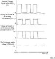
- the voltage level at Node B is controlled in a range between 0 and a value of (VDD1-Vthn), where Vthn is the threshold voltage of NMOS transistor M31. Therefore, introducing the NMOS transistor M31 into the I/O receiver may provide protection for the NMOS transistor M29 and the NMOS transistor M30.
- the gate electrode of the PMOS transistor M27 is connected to Port PAD so that leakage current from the power supply voltage VDD1 to ground (i.e. Port VSS) may be avoided.
- the voltage-level converting unit reduces the received voltage signal and converts the received voltage signal into an internal voltage signal. The internal voltage signal is transmitted into the internal chip through Port C.
- the maximum value of the voltage signal at Node B is (VDD1-Vthn), which cannot reach the operational power supply voltage VDD1 of the I/O receiver. Therefore, the operation speed of the I/O receiver may be reduced and the performance of the I/O receiver may be degraded.
- US6031393A discloses an input buffer to interface among devices on a main circuit board.
- the input buffer includes a first transistor coupled between a first terminal and an input terminal of an inverter.
- the first transistor has an enable terminal adapted to be coupled to a first voltage supply.
- a second transistor that is coupled between the first terminal and the input terminal is also included.
- the input buffer further includes a control circuit to enable the second transistor.
- the control circuit is coupled to the first terminal, an enable terminal of the second transistor, the input terminal, and an output terminal of the inverter.
- WO96/42139A1 discloses an output driver circuit and an input receiver circuit.
- the output driver circuit employs a series-connected pair of PMOS transistors and coupled to a series-connected pair of NMOS transistors.
- One of the PMOS transistors and one of the NMOS transistors have their gate terminals connected to a pair of power sources (Vref, VCC) such that these transistors maintain a voltage level on the node connecting the transistor to its corresponding pair.
- the voltage level is maintained during times when the pair of transistors are not conducting current. By maintaining this voltage, the voltage difference between any two terminals of the transistors is held within the maximum allowable voltage of the semiconductor technology.
- An input receiver circuit is also described which contains an NMOS transistor between the input conductor and receiving inverter circuits.
- This NMOS transistor has its gate terminal connected to a power supply (VCC) conveying the same voltage as the power supply for the integrated circuit core.
- VCC power supply
- the NMOS transistor (120) limits the voltage at the input of the receiving inverter circuits to no more than the power supply voltage (VCC).
- the circuits may be combined to form an input/output driver circuit.
- the present invention provides an input-output (I/O) receiver according to claim 1 of the appended claims.
- a first aspect of the present invention includes an input-output (I/O) receiver.
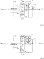
- the I/O receiver includes a receiving terminal, a first N-type metal-oxide-semiconductor (NMOS) transistor, a reformation circuit, and a compensation unit.
- the receiving terminal is coupled with an external voltage signal.
- the first NMOS transistor has a source electrode coupled with the receiving terminal and a gate electrode coupled with a first power supply voltage.
- the reformation circuit is configured to reform a voltage signal transmitted from a drain electrode of the first NMOS transistor.
- the compensation unit includes a first PMOS transistor, a second PMOS transistor, and a second NMOS transistor. Moreover, the compensation unit is configured to provide a compensation voltage to a voltage signal at the drain electrode of the first NMOS transistor thereby a maximum level of the voltage signal at the drain electrode of the first NMOS transistor reaches the first power supply voltage.
- the I/O receiver is configured so that, when the external voltage signal decreases from a logic-high voltage level to a logic-low voltage level: the first PMOS transistor is turned on; the second NMOS transistor is turned off; the voltage level at the drain electrode of the first PMOS transistor increases; and when the voltage level at the drain electrode of the first PMOS transistor becomes higher than the threshold voltage of the second PMOS transistor, the second PMOS transistor is turned off to let the output voltage level at the drain electrode of the first NMOS transistor drop to the logic-low voltage level.
- the I/O receiver is configured so that, when the external voltage signal decreases from a logic-high voltage level to a logic-low voltage level: the first PMOS transistor is turned on; the second NMOS transistor is turned off; the voltage level at the drain electrode of the first PMOS transistor increases; and when the voltage level at the drain electrode of the first PMOS transistor becomes higher than the threshold voltage of the second PMOS transistor, the second PMOS transistor is turned off and the third NMOS transistor is turned on to let the output voltage level at the drain electrode of the first NMOS transistor drop to the logic-low voltage level.
- the I/O receiver is configured so that, when the external voltage signal decreases from a logic-high voltage level to a logic-low voltage level: the third PMOS transistor and the fourth PMOS transistor of the inverter unit is turned on; the fourth NMOS transistor and the fifth NMOS transistor of the inverter unit is turned off; and the first power supply voltage drives an output voltage of the inverter unit to a logic-high voltage level.
- the source electrode of the second PMOS transistor P2 may be coupled with the first power supply voltage VDD1
- the gate electrode of the second PMOS transistor P2 may be coupled with the drain electrode of the first PMOS transistor P1
- the drain electrode of the second PMOS transistor P2 may be coupled with the drain electrode of the first NMOS transistor N1.
- the first PMOS transistor P1 may be turned off, while the second NMOS transistor N2 may be turned on.
- the drain electrode of the first PMOS transistor P1 may then be grounded through the second NMOS transistor N2.
- the voltage level of the drain electrode of the first PMOS transistor P1 may be pulled down.
- the second PMOS transistor P2 may be turned on so that the voltage level at Node B may reach the first power supply voltage VDD1.
- the first PMOS transistor P1 may be turned on, while the second NMOS transistor N2 may be turned off.
- the voltage level at the drain electrode of the first PMOS transistor P1 may increase.
- the second PMOS transistor P2 may be turned off so that the voltage level at Node B may drop to a logic-low voltage level.
- the drain electrode of the fourth NMOS transistor N4 may be coupled with the drain electrode of the fourth PMOS transistor P4, and the gate electrode of the fourth NMOS transistor N4 may be coupled with the drain electrode of the first NMOS transistor N1.
- the drain electrode of the fifth NMOS transistor N5 may be coupled with the source electrode of the fourth NMOS transistor N4, the source electrode of the fifth NMOS transistor N5 may be grounded, and the gate electrode of the fifth NMOS transistor N5 may be coupled with the drain electrode of the first NMOS transistor N1.
- the third PMOS transistor P3 and the fourth PMOS transistor P4 may be turned off, while the fourth NMOS transistor N4 and the fifth NMOS transistor N5 may be turned on.
- the ground VSS may pull down the voltage signal at the output terminal of the inverter unit to a logic-low voltage level.
- the third PMOS transistor P3 and the PMOS transistor P4 may be turned on while the fourth NMOS transistor N4 and the fifth NMOS transistor N5 may be turned off. Therefore, a first power supply voltage VDD1 may drive the voltage signal at the output terminal of the inverter unit to a logic-high voltage level.
- the drain electrode of the third NMOS transistor N3 may be coupled with the drain electrode of the second PMOS transistor P2 and also to the drain electrode of the first NMOS transistor N1, the gate electrode of the third NMOS transistor N3 may be coupled with the drain electrode of the first PMOS transistor P1, and the source electrode of the third NMOS transistor may be grounded.
- the output voltage of the NMOS transistor M31 i.e. the voltage signal at Node B
- the voltage signal at Node B may be in a range between 0 V and 0.7 V. That is, the maximum voltage level at Node B may only reach VDD1-Vthn. In such a case, the I/O receiver may still work, but the performance of the I/O receiver may be degraded.
- the voltage signal at Node B may be in a range between 0 V and 1.6 V. That is, the maximum voltage level at Node B may reach the first power supply voltage VDD1.
- the first PMOS transistor when the receiving terminal receives a high voltage level signal, the first PMOS transistor may be turned off while the second NMOS transistor may be turned on. Therefore, the voltage level at the drain electrode of the first PMOS transistor may be pulled down through the second NMOS transistor. Moreover, because the drain electrode of the first PMOS transistor may be coupled with the gate electrode of the second PMOS transistor, the second PMOS transistor may then be turned on. Since the drain electrode of the second PMOS transistor may be coupled with the drain electrode of the first NMOS transistor, the voltage at the drain electrode of the first NMOS transistor may reach the operation power supply voltage of the I/O receiver.
- the compensation unit may provide a compensation voltage to the voltage signal at the drain electrode of the first NMOS transistor such that the maximum level of the voltage signal at the drain electrode of the first NMOS transistor may reach the first power supply voltage. Therefore, with a simple circuit structure, the disclosed I/O receiver accepts external high voltage inputs and also improves the speed and performance of the I/O circuit.
Landscapes
- Engineering & Computer Science (AREA)
- Computer Hardware Design (AREA)
- Physics & Mathematics (AREA)
- Computing Systems (AREA)
- General Engineering & Computer Science (AREA)
- Mathematical Physics (AREA)
- Logic Circuits (AREA)
Claims (12)
- Eingabe-Ausgabe-, E/A-, Empfänger mit:einem Empfangsanschluss, der mit einem externen Spannungssignal gekoppelt ist;einem ersten NMOS-Transistor (N1) mit einer Source-Elektrode, die mit dem Empfangsanschluss gekoppelt ist, und einer Gate-Elektrode, die mit einer ersten Energieversorgungsspannung (VDD1) verbunden ist;einer Umformungsschaltung (202), die konfiguriert ist, die steigende Flanke und die fallende Flanke eines Spannungssignals, das von einer Drain-Elektrode des ersten NMOS-Transistors (N1) übertragen wurde, zu schärfen; undeiner Kompensationseinheit (201), die aufweist einen ersten PMOS-Transistor (P1), einen zweiten PMOS-Transistor (P2), einen zweiten NMOS-Transistor (N2) und einen dritten NMOS-Transistor (N3), wobei die Kompensationseinheit (201) konfiguriert ist, eine Kompensationsspannung an ein Spannungssignal an der Drain-Elektrode des ersten NMOS-Transistors (N1) bereitzustellen, wodurch ein Maximalpegel des Spannungssignals an der Drain-Elektrode des ersten NMOS-Transistors (N1) die erste Energieversorgungsspannung (VDD1) erreicht; wobei:eine Source-Elektrode des ersten PMOS-Transistors (P1) mit der ersten Energieversorgungsspannung (VDD1) gekoppelt ist und eine Gate-Elektrode des ersten PMOS-Transistors (P1) mit dem Empfangsanschluss gekoppelt ist;eine Drain-Elektrode des zweiten NMOS-Transistors (N2) mit einer Drain-Elektrode des ersten PMOS-Transistors (P1) gekoppelt ist, eine Gate-Elektrode des zweiten NMOS-Transistors (N2) mit der Drain-Elektrode des ersten NMOS-Transistors (N1) gekoppelt ist und eine Source-Elektrode des zweiten NMOS-Transistors (N2) mit Masse verbunden ist; undeine Drain-Elektrode des dritten NMOS-Transistors (N3) mit der Drain-Elektrode des zweiten PMOS-Transistors (P2) und der Drain-Elektrode des ersten NMOS-Transistors (N1) gekoppelt ist, eine Gate-Elektrode des dritten NMOS-Transistors (N3) mit der Drain-Elektrode des ersten PMOS-Transistors (P1) gekoppelt ist und eine Source-Elektrode des dritten NMOS-Transistors (N3) mit Masse verbunden ist.
- E/A-Empfänger gemäß Anspruch 1, wobei
eine Source-Elektrode des zweiten PMOS-Transistors (P2) mit der ersten Energieversorgungsspannung (VDD1) gekoppelt ist, eine Gate-Elektrode des zweiten PMOS-Transistors (P2) mit der Drain-Elektrode des ersten PMOS-Transistors (P1) gekoppelt ist und eine Drain-Elektrode des zweiten PMOS-Transistors (P2) mit der Drain-Elektrode des ersten NMOS-Transistors (N1) gekoppelt ist. - E/A-Empfänger gemäß Anspruch 2,
wobei, sobald das externe Spannungssignal sich von einem Logik-low-Spannungspegel auf einen Logik-high-Spannungspegel erhöht: der erste PMOS-Transistor (P1) ausgeschaltet wird; der zweite NMOS-Transistor (N2) eingeschaltet wird; ein Spannungspegel an der Drain-Elektrode des ersten PMOS-Transistors (P1) durch den zweiten NMOS-Transistor (N2) heruntergezogen wird; und sobald der Spannungspegel an der Drain-Elektrode des ersten PMOS-Transistors (P1) niedriger oder gleich einer Schwellspannung des zweiten PMOS-Transistors (P2) wird, der zweite PMOS-Transistor (P2) eingeschaltet wird, um den Ausgangsspannungspegel an der Drain-Elektrode des ersten NMOS-Transistors (N1) die erste Energieversorgungsspannung (VDD1) erreichen zu lassen; und/oder
wobei, sobald das externe Spannungssignal sich von einem Logik-high-Spannungspegel zu einem Logik-low-Spannungspegel verringert: der erste PMOS-Transistor (P1) eingeschaltet wird; der zweite NMOS-Transistor (N2) ausgeschaltet wird; der Spannungspegel an der Drain-Elektrode des ersten PMOS-Transistors (P1) sich erhöht; und sobald der Spannungspegel an der Drain-Elektrode des ersten PMOS-Transistors (P1) größer als die Schwellspannung des zweiten PMOS-Transistors (P2) wird, der zweite PMOS-Transistor (P2) ausgeschaltet wird, um den Ausgangsspannungspegel an der Drain-Elektrode des ersten NMOS-Transistors (N1) auf den Logik-low-Spannungspegel fallenzulassen. - E/A-Empfänger gemäß Anspruch 1,
wobei, sobald das externe Spannungssignal sich von einem Logik-low-Spannungspegel auf einen Logik-high-Spannungspegel erhöht: der erste PMOS-Transistor (P1) ausgeschaltet wird; der zweite NMOS-Transistor (N2) eingeschaltet wird; ein Spannungspegel an der Drain-Elektrode des ersten PMOS-Transistors (P1) durch den zweiten NMOS-Transistor (N2) heruntergezogen wird; und sobald der Spannungspegel an der Drain-Elektrode des ersten PMOS-Transistors (P1) niedriger als oder gleich einer Schwellspannung des zweiten PMOS-Transistors (P2) wird, der zweite PMOS-Transistor (P2) eingeschaltet wird und der dritte NMOS-Transistor (N3) ausgeschaltet wird, um den Ausgangsspannungspegel an der Drain-Elektrode des ersten NMOS-Transistors (N1) die erste Energieversorgungsspannung (VDD1) erreichen zu lassen; und/oder
wobei, sobald das externe Spannungssignal sich von einem Logik-high-Spannungspegel auf einen Logik-low-Spannungspegel verringert: der erste PMOS-Transistor (P1) eingeschaltet wird; der zweite NMOS-Transistor (N2) ausgeschaltet wird; der Spannungspegel an der Drain-Elektrode des ersten PMOS-Transistors (P1) sich erhöht; und sobald der Spannungspegel an der Drain-Elektrode des ersten PMOS-Transistors (P1) größer als die Schwellspannung des zweiten PMOS-Transistors (P2) wird, der zweite PMOS-Transistor (P2) ausgeschaltet wird und der dritte NMOS-Transistor (N3) eingeschaltet wird, um den Ausgangsspannungspegel der Drain-Elektrode des ersten NMOS-Transistors (N1) auf den Logik-low-Spannungspegel fallenzulassen. - E/A-Empfänger gemäß Anspruch 1, wobei die Umformungsschaltung (202) eine Inverter-Einheit ist.
- E/A-Empfänger gemäß Anspruch 5, wobei:die Inverter-Einheit einen dritten PMOS-Transistor (P3) und einen vierten NMOS-Transistor (N4) aufweist;eine Source-Elektrode des dritten PMOS-Transistors (P3) mit der ersten Energieversorgungsspannung (VDD1) gekoppelt ist, während eine Gate-Elektrode des dritten PMOS-Transistors (P3) mit der Drain-Elektrode des ersten NMOS-Transistors (N1) gekoppelt ist; undeine Drain-Elektrode des vierten NMOS-Transistors (N4) mit der Drain-Elektrode des dritten PMOS-Transistors (P3) gekoppelt ist, eine Source-Elektrode des vierten NMOS-Transistors (N4) mit Masse verbunden ist und eine Gate-Elektrode des vierten NMOS-Transistors (N4) mit der Drain-Elektrode des ersten NMOS-Transistors (N1) gekoppelt ist.
- E/A-Empfänger gemäß Anspruch 6,
wobei, sobald das externe Spannungssignal sich von einem Logik-low-Spannungspegel auf einen Logik-high-Spannungspegel erhöht: der dritte PMOS-Transistor (P3) der Inverter-Einheit ausgeschaltet wird; der vierte NMOS-Transistor (N4) der Inverter-Einheit eingeschaltet wird; und die Massen eine Ausgangsspannung der Inverter-Einheit auf einen Logik-low-Spannungspegel zieht; und/oder
wobei, sobald das externe Spannungssignal sich von einem Logik-high-Spannungspegel auf einen Logik-low-Spannungspegel verringert: der dritte PMOS-Transistor (P3) der Inverter-Einheit eingeschaltet wird; der vierte NMOS-Transistor (N4) der Inverter-Einheit ausgeschaltet wird; und die erste Energieversorgungsspannung (VDD1) eine Ausgangsspannung der Inverter-Einheit auf einen Logik-high-Spannungspegel treibt. - E/A-Empfänger gemäß Anspruch 5, wobei:die Inverter-Einheit einen dritten PMOS-Transistor (P3), einen vierten PMOS-Transistor, einen fünften NMOS-Transistor (N4) und einen fünften NMOS-Transistor aufweist;eine Source-Elektrode des dritten PMOS-Transistors (P3) mit der ersten Energieversorgungsspannung (VDD1) gekoppelt ist, während eine Gate-Elektrode des dritten PMOS-Transistors (P3) mit der Drain-Elektrode des ersten NMOS-Transistors (N1) gekoppelt ist;eine Source-Elektrode des vierten PMOS-Transistors mit einer Drain-Elektrode des dritten PMOS-Transistors (P3) gekoppelt ist, während eine Gate-Elektrode des vierten PMOS-Transistors mit der Drain-Elektrode des ersten NMOS-Transistors (N1) gekoppelt ist;eine Drain-Elektrode des vierten NMOS-Transistors (N4) mit einer Drain-Elektrode des vierten PMOS-Transistors gekoppelt ist, während eine Gate-Elektrode des vierten NMOS-Transistors (N4) mit der Drain-Elektrode des ersten NMOS-Transistors (N1) gekoppelt ist; undeine Drain-Elektrode des fünften NMOS-Transistors mit einer Source-Elektrode des vierten NMOS-Transistors (N4) gekoppelt ist, eine Source-Elektrode des vierten NMOS-Transistors mit Masse verbunden ist und eine Gate-Elektrode des vierten NMOS-Transistors (N4) mit der Drain-Elektrode des ersten NMOS-Transistors (N1) gekoppelt ist.
- E/A-Empfänger gemäß Anspruch 8,
wobei, sobald das externe Spannungssignal sich von einem Logik-low-Spannungspegel auf einen Logik-high-Spannungspegel erhöht: der dritte PMOS-Transistor (P3) und der vierte PMOS-Transistor der Inverter-Einheit ausgeschaltet werden; der vierte NMOS-Transistor (N4) und der fünfte NMOS-Transistor der Inverter-Einheit eingeschaltet werden; und die Masse eine Ausgangsspannung der Inverter-Einheit auf einen Logik-low-Spannungspegel zieht; und/oder
wobei, sobald das externe Spannungssignal sich von einem Logik-high-Spannungspegel auf einen Logik-low-Spannungspegel verringert: der dritte PMOS-Transistor (P3) und der vierte PMOS-Transistor der Inverter-Einheit eingeschaltet werden; der vierte NMOS-Transistor (N4) und der fünfte NMOS-Transistor der Inverter-Einheit ausgeschaltet werden; und die erste Energieversorgungsspannung (VDD1) eine Ausgangsspannung der Inverter-Einheit auf einen Logik-high-Spannungspegel treibt. - E/A-Empfänger gemäß einem der Ansprüche 1 bis 9, wobei die Umformungsschaltung (202) einen Eingangsanschluss aufweist, der mit der ersten Energieversorgungsspannung (VDD1) und der Drain-Elektrode des ersten NMOS-Transistors (N1) gekoppelt ist.
- E/A-Empfänger gemäß einem der Ansprüche 1 bis 10, wobei die Umformungsschaltung (202) ein Schmitt-Trigger ist.
- E/A-Empfänger gemäß einem der Ansprüche 1 bis 11, weiter aufweisend:
eine Spannungspegel-Konvertierungseinheit (203), die konfiguriert ist, einen Spannungspegel eines Ausgabesignals der Umformungsschaltung (202) zu konvertieren, wobei:ein Eingabeanschluss der Spannungspegel-Konvertierungseinheit (203) mit einem Ausgabeanschluss der Umformungsschaltung (202) und einer zweiten Energieversorgungsspannung gekoppelt ist; undein Ausgabeanschluss der Spannungspegel-Konvertierungseinheit (203) als ein Ausgabeanschluss des E/A-Empfängers dient.
Applications Claiming Priority (1)
| Application Number | Priority Date | Filing Date | Title |
|---|---|---|---|
| CN201610134366.7A CN107181482B (zh) | 2016-03-09 | 2016-03-09 | 输入输出接收电路 |
Publications (2)
| Publication Number | Publication Date |
|---|---|
| EP3217552A1 EP3217552A1 (de) | 2017-09-13 |
| EP3217552B1 true EP3217552B1 (de) | 2020-04-29 |
Family
ID=58261500
Family Applications (1)
| Application Number | Title | Priority Date | Filing Date |
|---|---|---|---|
| EP17158753.8A Active EP3217552B1 (de) | 2016-03-09 | 2017-03-01 | Ein- und ausgabeempfänger |
Country Status (3)
| Country | Link |
|---|---|
| US (1) | US10243564B2 (de) |
| EP (1) | EP3217552B1 (de) |
| CN (1) | CN107181482B (de) |
Families Citing this family (9)
| Publication number | Priority date | Publication date | Assignee | Title |
|---|---|---|---|---|
| CN107526700B (zh) * | 2016-06-22 | 2021-06-22 | 中芯国际集成电路制造(上海)有限公司 | 输入输出接收电路及电子装置 |
| CN107528580B (zh) * | 2017-09-22 | 2020-09-08 | 上海安其威微电子科技有限公司 | 电平转换电路 |
| US10965261B2 (en) | 2017-12-05 | 2021-03-30 | Qualcomm Incorporated | Power amplifier circuit |
| CN109787607B (zh) * | 2019-01-10 | 2023-05-26 | 苏州睿晟芯微电子科技有限公司 | 基于低压器件的高压高速io电路 |
| CN110048711B (zh) * | 2019-05-15 | 2023-11-21 | 苏州锴威特半导体股份有限公司 | 一种抵抗地和电源反弹噪声的数字信号处理电路 |
| CN111835373B (zh) * | 2019-11-18 | 2023-11-14 | 紫光同芯微电子有限公司 | 一种新型swp接口电路 |
| CN114793114B (zh) * | 2021-01-26 | 2025-03-11 | 深圳比特微电子科技有限公司 | 复合逻辑门电路和计算设备 |
| CN114189136B (zh) * | 2021-11-25 | 2024-02-06 | 上海华虹宏力半导体制造有限公司 | 一种放电电路 |
| CN119051634B (zh) * | 2024-10-29 | 2025-04-25 | 中科芯集成电路有限公司 | 一种具有防抖功能的边沿延时电路 |
Family Cites Families (12)
| Publication number | Priority date | Publication date | Assignee | Title |
|---|---|---|---|---|
| JPS5990292A (ja) * | 1982-11-12 | 1984-05-24 | Toshiba Corp | 電圧変換回路 |
| JP2567179B2 (ja) | 1992-03-18 | 1996-12-25 | 株式会社東芝 | レベル変換回路 |
| JP2658867B2 (ja) * | 1994-02-18 | 1997-09-30 | 日本電気株式会社 | レベル変換回路 |
| WO1996042139A1 (en) * | 1995-06-13 | 1996-12-27 | Advanced Micro Devices, Inc. | Input receiver, output driver, and input/output driver circuits capable of high voltage operation for an integrated circuit |
| US6031393A (en) * | 1997-12-31 | 2000-02-29 | Intel Corporation | Pass gate input buffer for a mixed voltage environment |
| US7504861B2 (en) * | 2003-11-20 | 2009-03-17 | Transpacific Ip, Ltd. | Input stage for mixed-voltage-tolerant buffer with reduced leakage |
| US8593203B2 (en) * | 2008-07-29 | 2013-11-26 | Qualcomm Incorporated | High signal level compliant input/output circuits |
| US8106699B2 (en) * | 2008-07-29 | 2012-01-31 | Qualcomm Incorporated | High signal level compliant input/output circuits |
| CN101753129B (zh) * | 2008-12-01 | 2011-11-30 | 中芯国际集成电路制造(上海)有限公司 | 可承受高电压的输出缓冲器 |
| CN103905028B (zh) * | 2012-12-25 | 2018-05-25 | 中芯国际集成电路制造(上海)有限公司 | 信号接收器和信号传输设备 |
| CN104158534B (zh) * | 2013-05-14 | 2017-06-23 | 中芯国际集成电路制造(上海)有限公司 | 用于i/o接口的降压转换电路 |
| KR102242582B1 (ko) * | 2014-10-10 | 2021-04-22 | 삼성전자주식회사 | 수신 회로 및 그것의 신호 수신 방법 |
-
2016
- 2016-03-09 CN CN201610134366.7A patent/CN107181482B/zh active Active
-
2017
- 2017-02-20 US US15/436,911 patent/US10243564B2/en active Active
- 2017-03-01 EP EP17158753.8A patent/EP3217552B1/de active Active
Non-Patent Citations (1)
| Title |
|---|
| None * |
Also Published As
| Publication number | Publication date |
|---|---|
| EP3217552A1 (de) | 2017-09-13 |
| US10243564B2 (en) | 2019-03-26 |
| CN107181482B (zh) | 2020-09-08 |
| CN107181482A (zh) | 2017-09-19 |
| US20170264297A1 (en) | 2017-09-14 |
Similar Documents
| Publication | Publication Date | Title |
|---|---|---|
| EP3217552B1 (de) | Ein- und ausgabeempfänger | |
| US8779739B2 (en) | Integrated DC converter with improved driving stage | |
| US20050017755A1 (en) | Low-to-high level shifter | |
| US20130181762A1 (en) | Current mirror modified level shifter | |
| US6791391B2 (en) | Level shifting circuit | |
| US7868659B2 (en) | I/O buffer with twice the supply voltage tolerance using normal supply voltage devices | |
| KR102739994B1 (ko) | 레벨 시프터의 트랜지션 지연 및 출력 스큐를 감소시키기 위한 장치 및 방법 | |
| CN103856205A (zh) | 电平转换电路、用于驱动高压器件的驱动电路以及相应的方法 | |
| US7446564B2 (en) | Level shifter | |
| CN104052454A (zh) | 用于高密度集成电路的电平转换器 | |
| CN112243569B (zh) | 半导体集成电路装置 | |
| EP2143206B1 (de) | Elektronische vorrichtung mit hochspannungstoleranter einheit | |
| US10135442B2 (en) | Current-mode logic circuit | |
| US10305481B2 (en) | Pre-driver for driving low voltage differential signaling (LVDS) driving circuit | |
| CN107181481B (zh) | 输入输出接收电路 | |
| US10482966B2 (en) | Block decoder of nonvolatile memory and level shifter | |
| JP2006033825A (ja) | レベルシフタ及びレベルシフティング方法 | |
| CN108712166B (zh) | 一种自适应电平转换电路 | |
| CN114389595B (zh) | 电平转换电路 | |
| US9935636B1 (en) | CMOS input buffer with low supply current and voltage down shifting | |
| CN101459424B (zh) | 输出单元、输入单元以及输入输出元件 | |
| US12323141B2 (en) | Level shifter | |
| US8570091B2 (en) | Level shifter | |
| WO2018193724A1 (ja) | 出力回路 | |
| US8502559B2 (en) | Level translator |
Legal Events
| Date | Code | Title | Description |
|---|---|---|---|
| PUAI | Public reference made under article 153(3) epc to a published international application that has entered the european phase |
Free format text: ORIGINAL CODE: 0009012 |
|
| STAA | Information on the status of an ep patent application or granted ep patent |
Free format text: STATUS: THE APPLICATION HAS BEEN PUBLISHED |
|
| AK | Designated contracting states |
Kind code of ref document: A1 Designated state(s): AL AT BE BG CH CY CZ DE DK EE ES FI FR GB GR HR HU IE IS IT LI LT LU LV MC MK MT NL NO PL PT RO RS SE SI SK SM TR |
|
| AX | Request for extension of the european patent |
Extension state: BA ME |
|
| STAA | Information on the status of an ep patent application or granted ep patent |
Free format text: STATUS: REQUEST FOR EXAMINATION WAS MADE |
|
| 17P | Request for examination filed |
Effective date: 20171106 |
|
| RBV | Designated contracting states (corrected) |
Designated state(s): AL AT BE BG CH CY CZ DE DK EE ES FI FR GB GR HR HU IE IS IT LI LT LU LV MC MK MT NL NO PL PT RO RS SE SI SK SM TR |
|
| STAA | Information on the status of an ep patent application or granted ep patent |
Free format text: STATUS: EXAMINATION IS IN PROGRESS |
|
| RAP1 | Party data changed (applicant data changed or rights of an application transferred) |
Owner name: SEMICONDUCTOR MANUFACTURING INTERNATIONAL (SHANGHA Owner name: SEMICONDUCTOR MANUFACTURING INTERNATIONAL (BEIJING |
|
| 17Q | First examination report despatched |
Effective date: 20181029 |
|
| GRAP | Despatch of communication of intention to grant a patent |
Free format text: ORIGINAL CODE: EPIDOSNIGR1 |
|
| STAA | Information on the status of an ep patent application or granted ep patent |
Free format text: STATUS: GRANT OF PATENT IS INTENDED |
|
| INTG | Intention to grant announced |
Effective date: 20191028 |
|
| GRAS | Grant fee paid |
Free format text: ORIGINAL CODE: EPIDOSNIGR3 |
|
| GRAA | (expected) grant |
Free format text: ORIGINAL CODE: 0009210 |
|
| STAA | Information on the status of an ep patent application or granted ep patent |
Free format text: STATUS: THE PATENT HAS BEEN GRANTED |
|
| AK | Designated contracting states |
Kind code of ref document: B1 Designated state(s): AL AT BE BG CH CY CZ DE DK EE ES FI FR GB GR HR HU IE IS IT LI LT LU LV MC MK MT NL NO PL PT RO RS SE SI SK SM TR |
|
| REG | Reference to a national code |
Ref country code: GB Ref legal event code: FG4D |
|
| REG | Reference to a national code |
Ref country code: CH Ref legal event code: EP |
|
| REG | Reference to a national code |
Ref country code: AT Ref legal event code: REF Ref document number: 1264847 Country of ref document: AT Kind code of ref document: T Effective date: 20200515 |
|
| REG | Reference to a national code |
Ref country code: DE Ref legal event code: R096 Ref document number: 602017015465 Country of ref document: DE |
|
| REG | Reference to a national code |
Ref country code: IE Ref legal event code: FG4D |
|
| REG | Reference to a national code |
Ref country code: NL Ref legal event code: MP Effective date: 20200429 |
|
| REG | Reference to a national code |
Ref country code: LT Ref legal event code: MG4D |
|
| PG25 | Lapsed in a contracting state [announced via postgrant information from national office to epo] |
Ref country code: LT Free format text: LAPSE BECAUSE OF FAILURE TO SUBMIT A TRANSLATION OF THE DESCRIPTION OR TO PAY THE FEE WITHIN THE PRESCRIBED TIME-LIMIT Effective date: 20200429 Ref country code: NO Free format text: LAPSE BECAUSE OF FAILURE TO SUBMIT A TRANSLATION OF THE DESCRIPTION OR TO PAY THE FEE WITHIN THE PRESCRIBED TIME-LIMIT Effective date: 20200729 Ref country code: SE Free format text: LAPSE BECAUSE OF FAILURE TO SUBMIT A TRANSLATION OF THE DESCRIPTION OR TO PAY THE FEE WITHIN THE PRESCRIBED TIME-LIMIT Effective date: 20200429 Ref country code: IS Free format text: LAPSE BECAUSE OF FAILURE TO SUBMIT A TRANSLATION OF THE DESCRIPTION OR TO PAY THE FEE WITHIN THE PRESCRIBED TIME-LIMIT Effective date: 20200829 Ref country code: FI Free format text: LAPSE BECAUSE OF FAILURE TO SUBMIT A TRANSLATION OF THE DESCRIPTION OR TO PAY THE FEE WITHIN THE PRESCRIBED TIME-LIMIT Effective date: 20200429 Ref country code: PT Free format text: LAPSE BECAUSE OF FAILURE TO SUBMIT A TRANSLATION OF THE DESCRIPTION OR TO PAY THE FEE WITHIN THE PRESCRIBED TIME-LIMIT Effective date: 20200831 Ref country code: GR Free format text: LAPSE BECAUSE OF FAILURE TO SUBMIT A TRANSLATION OF THE DESCRIPTION OR TO PAY THE FEE WITHIN THE PRESCRIBED TIME-LIMIT Effective date: 20200730 |
|
| REG | Reference to a national code |
Ref country code: AT Ref legal event code: MK05 Ref document number: 1264847 Country of ref document: AT Kind code of ref document: T Effective date: 20200429 |
|
| PG25 | Lapsed in a contracting state [announced via postgrant information from national office to epo] |
Ref country code: RS Free format text: LAPSE BECAUSE OF FAILURE TO SUBMIT A TRANSLATION OF THE DESCRIPTION OR TO PAY THE FEE WITHIN THE PRESCRIBED TIME-LIMIT Effective date: 20200429 Ref country code: LV Free format text: LAPSE BECAUSE OF FAILURE TO SUBMIT A TRANSLATION OF THE DESCRIPTION OR TO PAY THE FEE WITHIN THE PRESCRIBED TIME-LIMIT Effective date: 20200429 Ref country code: HR Free format text: LAPSE BECAUSE OF FAILURE TO SUBMIT A TRANSLATION OF THE DESCRIPTION OR TO PAY THE FEE WITHIN THE PRESCRIBED TIME-LIMIT Effective date: 20200429 Ref country code: BG Free format text: LAPSE BECAUSE OF FAILURE TO SUBMIT A TRANSLATION OF THE DESCRIPTION OR TO PAY THE FEE WITHIN THE PRESCRIBED TIME-LIMIT Effective date: 20200729 |
|
| PG25 | Lapsed in a contracting state [announced via postgrant information from national office to epo] |
Ref country code: NL Free format text: LAPSE BECAUSE OF FAILURE TO SUBMIT A TRANSLATION OF THE DESCRIPTION OR TO PAY THE FEE WITHIN THE PRESCRIBED TIME-LIMIT Effective date: 20200429 Ref country code: AL Free format text: LAPSE BECAUSE OF FAILURE TO SUBMIT A TRANSLATION OF THE DESCRIPTION OR TO PAY THE FEE WITHIN THE PRESCRIBED TIME-LIMIT Effective date: 20200429 |
|
| PG25 | Lapsed in a contracting state [announced via postgrant information from national office to epo] |
Ref country code: CZ Free format text: LAPSE BECAUSE OF FAILURE TO SUBMIT A TRANSLATION OF THE DESCRIPTION OR TO PAY THE FEE WITHIN THE PRESCRIBED TIME-LIMIT Effective date: 20200429 Ref country code: IT Free format text: LAPSE BECAUSE OF FAILURE TO SUBMIT A TRANSLATION OF THE DESCRIPTION OR TO PAY THE FEE WITHIN THE PRESCRIBED TIME-LIMIT Effective date: 20200429 Ref country code: DK Free format text: LAPSE BECAUSE OF FAILURE TO SUBMIT A TRANSLATION OF THE DESCRIPTION OR TO PAY THE FEE WITHIN THE PRESCRIBED TIME-LIMIT Effective date: 20200429 Ref country code: EE Free format text: LAPSE BECAUSE OF FAILURE TO SUBMIT A TRANSLATION OF THE DESCRIPTION OR TO PAY THE FEE WITHIN THE PRESCRIBED TIME-LIMIT Effective date: 20200429 Ref country code: SM Free format text: LAPSE BECAUSE OF FAILURE TO SUBMIT A TRANSLATION OF THE DESCRIPTION OR TO PAY THE FEE WITHIN THE PRESCRIBED TIME-LIMIT Effective date: 20200429 Ref country code: AT Free format text: LAPSE BECAUSE OF FAILURE TO SUBMIT A TRANSLATION OF THE DESCRIPTION OR TO PAY THE FEE WITHIN THE PRESCRIBED TIME-LIMIT Effective date: 20200429 Ref country code: RO Free format text: LAPSE BECAUSE OF FAILURE TO SUBMIT A TRANSLATION OF THE DESCRIPTION OR TO PAY THE FEE WITHIN THE PRESCRIBED TIME-LIMIT Effective date: 20200429 Ref country code: ES Free format text: LAPSE BECAUSE OF FAILURE TO SUBMIT A TRANSLATION OF THE DESCRIPTION OR TO PAY THE FEE WITHIN THE PRESCRIBED TIME-LIMIT Effective date: 20200429 |
|
| REG | Reference to a national code |
Ref country code: DE Ref legal event code: R097 Ref document number: 602017015465 Country of ref document: DE |
|
| PG25 | Lapsed in a contracting state [announced via postgrant information from national office to epo] |
Ref country code: SK Free format text: LAPSE BECAUSE OF FAILURE TO SUBMIT A TRANSLATION OF THE DESCRIPTION OR TO PAY THE FEE WITHIN THE PRESCRIBED TIME-LIMIT Effective date: 20200429 Ref country code: PL Free format text: LAPSE BECAUSE OF FAILURE TO SUBMIT A TRANSLATION OF THE DESCRIPTION OR TO PAY THE FEE WITHIN THE PRESCRIBED TIME-LIMIT Effective date: 20200429 |
|
| PLBE | No opposition filed within time limit |
Free format text: ORIGINAL CODE: 0009261 |
|
| STAA | Information on the status of an ep patent application or granted ep patent |
Free format text: STATUS: NO OPPOSITION FILED WITHIN TIME LIMIT |
|
| 26N | No opposition filed |
Effective date: 20210201 |
|
| PG25 | Lapsed in a contracting state [announced via postgrant information from national office to epo] |
Ref country code: SI Free format text: LAPSE BECAUSE OF FAILURE TO SUBMIT A TRANSLATION OF THE DESCRIPTION OR TO PAY THE FEE WITHIN THE PRESCRIBED TIME-LIMIT Effective date: 20200429 |
|
| PG25 | Lapsed in a contracting state [announced via postgrant information from national office to epo] |
Ref country code: MC Free format text: LAPSE BECAUSE OF FAILURE TO SUBMIT A TRANSLATION OF THE DESCRIPTION OR TO PAY THE FEE WITHIN THE PRESCRIBED TIME-LIMIT Effective date: 20200429 |
|
| REG | Reference to a national code |
Ref country code: CH Ref legal event code: PL |
|
| GBPC | Gb: european patent ceased through non-payment of renewal fee |
Effective date: 20210301 |
|
| REG | Reference to a national code |
Ref country code: BE Ref legal event code: MM Effective date: 20210331 |
|
| PG25 | Lapsed in a contracting state [announced via postgrant information from national office to epo] |
Ref country code: LU Free format text: LAPSE BECAUSE OF NON-PAYMENT OF DUE FEES Effective date: 20210301 Ref country code: LI Free format text: LAPSE BECAUSE OF NON-PAYMENT OF DUE FEES Effective date: 20210331 Ref country code: CH Free format text: LAPSE BECAUSE OF NON-PAYMENT OF DUE FEES Effective date: 20210331 Ref country code: FR Free format text: LAPSE BECAUSE OF NON-PAYMENT OF DUE FEES Effective date: 20210331 Ref country code: IE Free format text: LAPSE BECAUSE OF NON-PAYMENT OF DUE FEES Effective date: 20210301 Ref country code: GB Free format text: LAPSE BECAUSE OF NON-PAYMENT OF DUE FEES Effective date: 20210301 |
|
| PG25 | Lapsed in a contracting state [announced via postgrant information from national office to epo] |
Ref country code: BE Free format text: LAPSE BECAUSE OF NON-PAYMENT OF DUE FEES Effective date: 20210331 |
|
| PG25 | Lapsed in a contracting state [announced via postgrant information from national office to epo] |
Ref country code: HU Free format text: LAPSE BECAUSE OF FAILURE TO SUBMIT A TRANSLATION OF THE DESCRIPTION OR TO PAY THE FEE WITHIN THE PRESCRIBED TIME-LIMIT; INVALID AB INITIO Effective date: 20170301 |
|
| PG25 | Lapsed in a contracting state [announced via postgrant information from national office to epo] |
Ref country code: CY Free format text: LAPSE BECAUSE OF FAILURE TO SUBMIT A TRANSLATION OF THE DESCRIPTION OR TO PAY THE FEE WITHIN THE PRESCRIBED TIME-LIMIT Effective date: 20200429 |
|
| PG25 | Lapsed in a contracting state [announced via postgrant information from national office to epo] |
Ref country code: MK Free format text: LAPSE BECAUSE OF FAILURE TO SUBMIT A TRANSLATION OF THE DESCRIPTION OR TO PAY THE FEE WITHIN THE PRESCRIBED TIME-LIMIT Effective date: 20200429 |
|
| PG25 | Lapsed in a contracting state [announced via postgrant information from national office to epo] |
Ref country code: MT Free format text: LAPSE BECAUSE OF FAILURE TO SUBMIT A TRANSLATION OF THE DESCRIPTION OR TO PAY THE FEE WITHIN THE PRESCRIBED TIME-LIMIT Effective date: 20200429 |
|
| PG25 | Lapsed in a contracting state [announced via postgrant information from national office to epo] |
Ref country code: TR Free format text: LAPSE BECAUSE OF FAILURE TO SUBMIT A TRANSLATION OF THE DESCRIPTION OR TO PAY THE FEE WITHIN THE PRESCRIBED TIME-LIMIT Effective date: 20200429 |
|
| PGFP | Annual fee paid to national office [announced via postgrant information from national office to epo] |
Ref country code: DE Payment date: 20260319 Year of fee payment: 10 |