EP3217552B1 - Input-output receiver - Google Patents
Input-output receiver Download PDFInfo
- Publication number
- EP3217552B1 EP3217552B1 EP17158753.8A EP17158753A EP3217552B1 EP 3217552 B1 EP3217552 B1 EP 3217552B1 EP 17158753 A EP17158753 A EP 17158753A EP 3217552 B1 EP3217552 B1 EP 3217552B1
- Authority
- EP
- European Patent Office
- Prior art keywords
- nmos transistor
- pmos transistor
- drain electrode
- transistor
- coupled
- Prior art date
- Legal status (The legal status is an assumption and is not a legal conclusion. Google has not performed a legal analysis and makes no representation as to the accuracy of the status listed.)
- Active
Links
Images

Classifications
-
- H—ELECTRICITY
- H03—ELECTRONIC CIRCUITRY
- H03K—PULSE TECHNIQUE
- H03K19/00—Logic circuits, i.e. having at least two inputs acting on one output; Inverting circuits
- H03K19/0175—Coupling arrangements; Interface arrangements
- H03K19/0185—Coupling arrangements; Interface arrangements using field effect transistors only
- H03K19/018507—Interface arrangements
- H03K19/018521—Interface arrangements of complementary type, e.g. CMOS
-
- H—ELECTRICITY
- H03—ELECTRONIC CIRCUITRY
- H03K—PULSE TECHNIQUE
- H03K19/00—Logic circuits, i.e. having at least two inputs acting on one output; Inverting circuits
- H03K19/003—Modifications for increasing the reliability for protection
- H03K19/00315—Modifications for increasing the reliability for protection in field-effect transistor circuits
-
- H—ELECTRICITY
- H03—ELECTRONIC CIRCUITRY
- H03K—PULSE TECHNIQUE
- H03K19/00—Logic circuits, i.e. having at least two inputs acting on one output; Inverting circuits
- H03K19/01—Modifications for accelerating switching
- H03K19/017—Modifications for accelerating switching in field-effect transistor circuits
- H03K19/01707—Modifications for accelerating switching in field-effect transistor circuits in asynchronous circuits
- H03K19/01721—Modifications for accelerating switching in field-effect transistor circuits in asynchronous circuits by means of a pull-up or down element
-
- H—ELECTRICITY
- H03—ELECTRONIC CIRCUITRY
- H03K—PULSE TECHNIQUE
- H03K3/00—Circuits for generating electric pulses; Monostable, bistable or multistable circuits
- H03K3/02—Generators characterised by the type of circuit or by the means used for producing pulses
- H03K3/353—Generators characterised by the type of circuit or by the means used for producing pulses by the use, as active elements, of field-effect transistors with internal or external positive feedback
- H03K3/356—Bistable circuits
- H03K3/3565—Bistables with hysteresis, e.g. Schmitt trigger
Definitions
- the source electrode of the NMOS transistor M31 is coupled with Port PAD, while the gate electrode of the NMOS transistor M31 is coupled with the power supply voltage VDD1.
- the voltage level at Node B is controlled in a range between 0 and a value of (VDD1-Vthn), where Vthn is the threshold voltage of NMOS transistor M31. Therefore, introducing the NMOS transistor M31 into the I/O receiver may provide protection for the NMOS transistor M29 and the NMOS transistor M30.
- the gate electrode of the PMOS transistor M27 is connected to Port PAD so that leakage current from the power supply voltage VDD1 to ground (i.e. Port VSS) may be avoided.
- the voltage-level converting unit reduces the received voltage signal and converts the received voltage signal into an internal voltage signal. The internal voltage signal is transmitted into the internal chip through Port C.
- the maximum value of the voltage signal at Node B is (VDD1-Vthn), which cannot reach the operational power supply voltage VDD1 of the I/O receiver. Therefore, the operation speed of the I/O receiver may be reduced and the performance of the I/O receiver may be degraded.
- US6031393A discloses an input buffer to interface among devices on a main circuit board.
- the input buffer includes a first transistor coupled between a first terminal and an input terminal of an inverter.
- the first transistor has an enable terminal adapted to be coupled to a first voltage supply.
- a second transistor that is coupled between the first terminal and the input terminal is also included.
- the input buffer further includes a control circuit to enable the second transistor.
- the control circuit is coupled to the first terminal, an enable terminal of the second transistor, the input terminal, and an output terminal of the inverter.
- WO96/42139A1 discloses an output driver circuit and an input receiver circuit.
- the output driver circuit employs a series-connected pair of PMOS transistors and coupled to a series-connected pair of NMOS transistors.
- One of the PMOS transistors and one of the NMOS transistors have their gate terminals connected to a pair of power sources (Vref, VCC) such that these transistors maintain a voltage level on the node connecting the transistor to its corresponding pair.
- the voltage level is maintained during times when the pair of transistors are not conducting current. By maintaining this voltage, the voltage difference between any two terminals of the transistors is held within the maximum allowable voltage of the semiconductor technology.
- An input receiver circuit is also described which contains an NMOS transistor between the input conductor and receiving inverter circuits.
- This NMOS transistor has its gate terminal connected to a power supply (VCC) conveying the same voltage as the power supply for the integrated circuit core.
- VCC power supply
- the NMOS transistor (120) limits the voltage at the input of the receiving inverter circuits to no more than the power supply voltage (VCC).
- the circuits may be combined to form an input/output driver circuit.
- the present invention provides an input-output (I/O) receiver according to claim 1 of the appended claims.
- a first aspect of the present invention includes an input-output (I/O) receiver.
- the I/O receiver includes a receiving terminal, a first N-type metal-oxide-semiconductor (NMOS) transistor, a reformation circuit, and a compensation unit.
- the receiving terminal is coupled with an external voltage signal.
- the first NMOS transistor has a source electrode coupled with the receiving terminal and a gate electrode coupled with a first power supply voltage.
- the reformation circuit is configured to reform a voltage signal transmitted from a drain electrode of the first NMOS transistor.
- the compensation unit includes a first PMOS transistor, a second PMOS transistor, and a second NMOS transistor. Moreover, the compensation unit is configured to provide a compensation voltage to a voltage signal at the drain electrode of the first NMOS transistor thereby a maximum level of the voltage signal at the drain electrode of the first NMOS transistor reaches the first power supply voltage.
- the I/O receiver is configured so that, when the external voltage signal decreases from a logic-high voltage level to a logic-low voltage level: the first PMOS transistor is turned on; the second NMOS transistor is turned off; the voltage level at the drain electrode of the first PMOS transistor increases; and when the voltage level at the drain electrode of the first PMOS transistor becomes higher than the threshold voltage of the second PMOS transistor, the second PMOS transistor is turned off to let the output voltage level at the drain electrode of the first NMOS transistor drop to the logic-low voltage level.
- the I/O receiver is configured so that, when the external voltage signal decreases from a logic-high voltage level to a logic-low voltage level: the first PMOS transistor is turned on; the second NMOS transistor is turned off; the voltage level at the drain electrode of the first PMOS transistor increases; and when the voltage level at the drain electrode of the first PMOS transistor becomes higher than the threshold voltage of the second PMOS transistor, the second PMOS transistor is turned off and the third NMOS transistor is turned on to let the output voltage level at the drain electrode of the first NMOS transistor drop to the logic-low voltage level.
- the I/O receiver is configured so that, when the external voltage signal decreases from a logic-high voltage level to a logic-low voltage level: the third PMOS transistor and the fourth PMOS transistor of the inverter unit is turned on; the fourth NMOS transistor and the fifth NMOS transistor of the inverter unit is turned off; and the first power supply voltage drives an output voltage of the inverter unit to a logic-high voltage level.
- the source electrode of the second PMOS transistor P2 may be coupled with the first power supply voltage VDD1
- the gate electrode of the second PMOS transistor P2 may be coupled with the drain electrode of the first PMOS transistor P1
- the drain electrode of the second PMOS transistor P2 may be coupled with the drain electrode of the first NMOS transistor N1.
- the first PMOS transistor P1 may be turned off, while the second NMOS transistor N2 may be turned on.
- the drain electrode of the first PMOS transistor P1 may then be grounded through the second NMOS transistor N2.
- the voltage level of the drain electrode of the first PMOS transistor P1 may be pulled down.
- the second PMOS transistor P2 may be turned on so that the voltage level at Node B may reach the first power supply voltage VDD1.
- the first PMOS transistor P1 may be turned on, while the second NMOS transistor N2 may be turned off.
- the voltage level at the drain electrode of the first PMOS transistor P1 may increase.
- the second PMOS transistor P2 may be turned off so that the voltage level at Node B may drop to a logic-low voltage level.
- the drain electrode of the fourth NMOS transistor N4 may be coupled with the drain electrode of the fourth PMOS transistor P4, and the gate electrode of the fourth NMOS transistor N4 may be coupled with the drain electrode of the first NMOS transistor N1.
- the drain electrode of the fifth NMOS transistor N5 may be coupled with the source electrode of the fourth NMOS transistor N4, the source electrode of the fifth NMOS transistor N5 may be grounded, and the gate electrode of the fifth NMOS transistor N5 may be coupled with the drain electrode of the first NMOS transistor N1.
- the third PMOS transistor P3 and the fourth PMOS transistor P4 may be turned off, while the fourth NMOS transistor N4 and the fifth NMOS transistor N5 may be turned on.
- the ground VSS may pull down the voltage signal at the output terminal of the inverter unit to a logic-low voltage level.
- the third PMOS transistor P3 and the PMOS transistor P4 may be turned on while the fourth NMOS transistor N4 and the fifth NMOS transistor N5 may be turned off. Therefore, a first power supply voltage VDD1 may drive the voltage signal at the output terminal of the inverter unit to a logic-high voltage level.
- the drain electrode of the third NMOS transistor N3 may be coupled with the drain electrode of the second PMOS transistor P2 and also to the drain electrode of the first NMOS transistor N1, the gate electrode of the third NMOS transistor N3 may be coupled with the drain electrode of the first PMOS transistor P1, and the source electrode of the third NMOS transistor may be grounded.
- the output voltage of the NMOS transistor M31 i.e. the voltage signal at Node B
- the voltage signal at Node B may be in a range between 0 V and 0.7 V. That is, the maximum voltage level at Node B may only reach VDD1-Vthn. In such a case, the I/O receiver may still work, but the performance of the I/O receiver may be degraded.
- the voltage signal at Node B may be in a range between 0 V and 1.6 V. That is, the maximum voltage level at Node B may reach the first power supply voltage VDD1.
- the first PMOS transistor when the receiving terminal receives a high voltage level signal, the first PMOS transistor may be turned off while the second NMOS transistor may be turned on. Therefore, the voltage level at the drain electrode of the first PMOS transistor may be pulled down through the second NMOS transistor. Moreover, because the drain electrode of the first PMOS transistor may be coupled with the gate electrode of the second PMOS transistor, the second PMOS transistor may then be turned on. Since the drain electrode of the second PMOS transistor may be coupled with the drain electrode of the first NMOS transistor, the voltage at the drain electrode of the first NMOS transistor may reach the operation power supply voltage of the I/O receiver.
- the compensation unit may provide a compensation voltage to the voltage signal at the drain electrode of the first NMOS transistor such that the maximum level of the voltage signal at the drain electrode of the first NMOS transistor may reach the first power supply voltage. Therefore, with a simple circuit structure, the disclosed I/O receiver accepts external high voltage inputs and also improves the speed and performance of the I/O circuit.
Landscapes
- Engineering & Computer Science (AREA)
- Computer Hardware Design (AREA)
- Physics & Mathematics (AREA)
- Computing Systems (AREA)
- General Engineering & Computer Science (AREA)
- Mathematical Physics (AREA)
- Logic Circuits (AREA)
Description
- This application claims the priority of Chinese Patent Application No.
CN201610134366.7, filed on March 9, 2016 - The present invention generally relates to the field of semiconductor integrated circuits (ICs) and, more particularly, relates to input-output receivers and operation mechanism thereof.
- An input-output (I/O) receiver is an interface circuit for internal and external signal exchange of an IC chip. The main function of an I/O receiver is to receive digital/analog signals. In some applications, the external voltage may be higher than the internal power supply voltage of the chip. Therefore, a voltage resistant circuit is commonly designed in an I/O receiver in order to protect the I/O receiver.
-
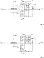
Figure 1 shows a schematic view of an existing I/O receiver. Referring toFigure 1 , the receiving terminal receives signals from Port PAD. The voltage level Vin at Port PAD is higher than the power supply voltage VDD1 of the receiver. When the signal at Port PAD is directly transmitted to Node B, a high voltage level may cause reliability issues of NMOS transistors M29 and M30. Therefore, the I/O receiver further includes an NMOS transistor M31 to reduce the maximum level of the voltage signal at Node B. - As shown in
Figure 1 , the source electrode of the NMOS transistor M31 is coupled with Port PAD, while the gate electrode of the NMOS transistor M31 is coupled with the power supply voltage VDD1. Thus, the voltage level at Node B is controlled in a range between 0 and a value of (VDD1-Vthn), where Vthn is the threshold voltage of NMOS transistor M31. Therefore, introducing the NMOS transistor M31 into the I/O receiver may provide protection for the NMOS transistor M29 and the NMOS transistor M30. Further, the gate electrode of the PMOS transistor M27 is connected to Port PAD so that leakage current from the power supply voltage VDD1 to ground (i.e. Port VSS) may be avoided. Moreover, the voltage-level converting unit reduces the received voltage signal and converts the received voltage signal into an internal voltage signal. The internal voltage signal is transmitted into the internal chip through Port C. - However, in existing I/O receivers, the maximum value of the voltage signal at Node B is (VDD1-Vthn), which cannot reach the operational power supply voltage VDD1 of the I/O receiver. Therefore, the operation speed of the I/O receiver may be reduced and the performance of the I/O receiver may be degraded.
- The disclosed I/O receivers are directed to solve one or more problems set forth above and other problems in the art.
-
US6031393A discloses an input buffer to interface among devices on a main circuit board. The input buffer includes a first transistor coupled between a first terminal and an input terminal of an inverter. The first transistor has an enable terminal adapted to be coupled to a first voltage supply. A second transistor that is coupled between the first terminal and the input terminal is also included. The input buffer further includes a control circuit to enable the second transistor. The control circuit is coupled to the first terminal, an enable terminal of the second transistor, the input terminal, and an output terminal of the inverter. -
WO96/42139A1 -
US2010/026363A1 discloses high signal level compliant input/output circuits. A level shifter has at least one of either a pull up or a pull down circuit. The circuit is made of electronic components with reliability limits less than a maximum signal level output by the level shifter. The level shifter also has a timing circuit coupled to at least one of either the pull up or pull down circuit. The timing circuit controls a time of application of an input signal to at least one of either the pull up or pull down circuit preventing a terminal to terminal signal level experienced by the electronic components exceeding the reliability limits. - The present invention provides an input-output (I/O) receiver according to
claim 1 of the appended claims. - A first aspect of the present invention includes an input-output (I/O) receiver. The I/O receiver includes a receiving terminal, a first N-type metal-oxide-semiconductor (NMOS) transistor, a reformation circuit, and a compensation unit. The receiving terminal is coupled with an external voltage signal. The first NMOS transistor has a source electrode coupled with the receiving terminal and a gate electrode coupled with a first power supply voltage. The reformation circuit is configured to reform a voltage signal transmitted from a drain electrode of the first NMOS transistor. The compensation unit includes a first PMOS transistor, a second PMOS transistor, and a second NMOS transistor. Moreover, the compensation unit is configured to provide a compensation voltage to a voltage signal at the drain electrode of the first NMOS transistor thereby a maximum level of the voltage signal at the drain electrode of the first NMOS transistor reaches the first power supply voltage.
- Further, a source electrode of the first PMOS transistor is coupled with the first power supply voltage and a gate electrode of the first PMOS transistor is coupled with the receiving terminal. Preferably, a drain electrode of the second NMOS transistor is coupled with a drain electrode of the first PMOS transistor, a gate electrode of the second NMOS transistor is coupled with the drain electrode of the first NMOS transistor, and a source electrode of the second NMOS transistor is connected to ground.
- According to a first embodiment, preferably, a source electrode of the second PMOS transistor is coupled with the first power supply voltage, a gate electrode of the second PMOS transistor is coupled with the drain electrode of the first PMOS transistor, and a drain electrode of the second PMOS transistor is coupled with the drain electrode of the first NMOS transistor.
- In the first embodiment, preferably, the I/O receiver is configured so that, when the external voltage signal increases from a logic-low voltage level to a logic-high voltage level: the first PMOS transistor is turned off; the second NMOS transistor is turned on; a voltage level at the drain electrode of the first PMOS transistor is pulled down through the second NMOS transistor; and when the voltage level at the drain electrode of the first PMOS transistor becomes less than or equal to a threshold voltage of the second PMOS transistor, the second PMOS transistor is turned on to let the output voltage level at the drain electrode of the first NMOS transistor reach the first power supply voltage.
- In the first embodiment, preferably, the I/O receiver is configured so that, when the external voltage signal decreases from a logic-high voltage level to a logic-low voltage level: the first PMOS transistor is turned on; the second NMOS transistor is turned off; the voltage level at the drain electrode of the first PMOS transistor increases; and when the voltage level at the drain electrode of the first PMOS transistor becomes higher than the threshold voltage of the second PMOS transistor, the second PMOS transistor is turned off to let the output voltage level at the drain electrode of the first NMOS transistor drop to the logic-low voltage level.
- According to an aspect of the invention, the compensation unit further includes a third NMOS transistor; and a drain electrode of the third NMOS transistor is coupled with the drain electrode of the second PMOS transistor and the drain electrode of the first NMOS transistor, a gate electrode of the third NMOS transistor is coupled with the drain electrode of the first PMOS transistor, and a source electrode of the third NMOS transistor is grounded.
- In a second embodiment, preferably, the I/O receiver is configured so that, when the external voltage signal increases from a logic-low voltage level to a logic-high voltage level: the first PMOS transistor is turned off; the second NMOS transistor is turned on; a voltage level at the drain electrode of the first PMOS transistor is pulled down through the second NMOS transistor; and when the voltage level at the drain electrode of the first PMOS transistor becomes less than or equal to a threshold voltage of the second PMOS transistor, the second PMOS transistor is turned on and the third NMOS transistor is turned off to let the output voltage level at the drain electrode of the first NMOS transistor reach the first power supply voltage.
- In the second embodiment, preferably, the I/O receiver is configured so that, when the external voltage signal decreases from a logic-high voltage level to a logic-low voltage level: the first PMOS transistor is turned on; the second NMOS transistor is turned off; the voltage level at the drain electrode of the first PMOS transistor increases; and when the voltage level at the drain electrode of the first PMOS transistor becomes higher than the threshold voltage of the second PMOS transistor, the second PMOS transistor is turned off and the third NMOS transistor is turned on to let the output voltage level at the drain electrode of the first NMOS transistor drop to the logic-low voltage level.
- In a third embodiment, preferably, the reformation circuit is an inverter unit.
- In a first alternative of the third embodiment, preferably, the inverter unit includes a third PMOS transistor and a fourth NMOS transistor; a source electrode of the third PMOS transistor is coupled with the first power supply voltage while a gate electrode of the third PMOS transistor is coupled with the drain electrode of the first NMOS transistor; and a drain electrode of the fourth NMOS transistor is coupled with the drain electrode of the third PMOS transistor, a source electrode of the fourth NMOS transistor is grounded, and a gate electrode of the fourth NMOS transistor is coupled with the drain electrode of the first NMOS transistor.
- In the first alternative of the third embodiment, preferably, the I/O receiver is configured so that, when the external voltage signal increase from a logic-low voltage level to a logic-high voltage level: the third PMOS transistor of the inverter unit is turned off; the fourth NMOS transistor of the inverter unit is turned on; and the ground pulls down an output voltage of the inverter unit to a logic-low voltage level.
- In the first alternative of the third embodiment, preferably, the I/O receiver is configured so that, when the external voltage signal decreases from a logic-high voltage level to a logic-low voltage level: the third PMOS transistor of the inverter unit is turned on; the fourth NMOS transistor of the inverter unit is turned off; and the first power supply voltage drives an output voltage of the inverter unit to a logic-high voltage level.
- In a first alternative of the third embodiment, preferably, the inverter unit includes a third PMOS transistor, a fourth PMOS transistor, a fourth NMOS transistor, and a fifth NMOS transistor; a source electrode of the third PMOS transistor is coupled with the first power supply voltage while a gate electrode of the third PMOS transistor is coupled with the drain electrode of the first NMOS transistor; a source electrode of the fourth PMOS transistor is coupled with a drain electrode of the third PMOS transistor while a gate electrode of the fourth PMOS transistor is coupled with the drain electrode of the first NMOS transistor; a drain electrode of the fourth NMOS transistor is coupled with a drain electrode of the fourth PMOS transistor while a gate electrode of the fourth NMOS transistor is coupled with the drain electrode of the first NMOS transistor; and a drain electrode of the fifth NMOS transistor is coupled with a source electrode of the fourth NMOS transistor, a source electrode of the fifth NMOS transistor is grounded, and a gate electrode of the fourth NMOS transistor is coupled with the drain electrode of the first NMOS transistor.
- In the second alternative of the third embodiment, preferably, the I/O receiver is configured so that, when the external voltage signal increases from a logic-low voltage level to a logic-high voltage level: the third PMOS transistor and the fourth PMOS transistor of the inverter unit are turned off; the fourth NMOS transistor and the fifth NMOS transistor of the inverter unit is turned on; and the ground pulls down an output voltage of the inverter unit to a logic-low voltage level.
- In the second alternative of the third embodiment, preferably, the I/O receiver is configured so that, when the external voltage signal decreases from a logic-high voltage level to a logic-low voltage level: the third PMOS transistor and the fourth PMOS transistor of the inverter unit is turned on; the fourth NMOS transistor and the fifth NMOS transistor of the inverter unit is turned off; and the first power supply voltage drives an output voltage of the inverter unit to a logic-high voltage level.
- In all embodiments, preferably, the reformation circuit has an input terminal coupled with the first power supply voltage and the drain electrode of the first NMOS transistor.
- In all embodiments, preferably, the reformation circuit is a Schmitt trigger.
- In all embodiments, preferably, the I/O receiver further includes: a voltage-level converting unit, configured to convert a voltage level of an output signal of the reformation circuit, wherein: an input terminal of the voltage-level converting unit is coupled with an output terminal of the reformation circuit and a second power supply voltage; and an output terminal of the voltage-level converting unit serves as an output terminal of the I/O receiver.
- Other aspects of the present invention can be understood by those skilled in the art in light of the description, the claims, and the drawings of the present disclosure.
- The following drawings are merely examples for illustrative purposes according to various disclosed embodiments and are not intended to limit the scope of the present disclosure.
-
Figure 1 illustrates a schematic view of the circuit structure of an existing I/O receiver; -
Figure 2 illustrates a schematic view of a circuit structure of an exemplary I/O receiver; -
Figure 3 illustrates a schematic view of a circuit structure of another exemplary I/O receiver; -
Figure 4 illustrates a schematic view of a circuit structure of another exemplary I/O receiver consistent with disclosed embodiments; and -
Figure 5 illustrates simulated voltage profiles at certain positions in an exemplary I/O receiver consistent with disclosed embodiments and also in an existing I/O receiver. - Reference will now be made in detail to exemplary embodiments of the invention, which are illustrated in the accompanying drawings. Wherever possible, the same reference numbers will be used throughout the drawings to refer to the same or like parts.
-
Figure 2 shows a schematic view of a circuit structure of an exemplary I/O receiver. Referring toFigure 2 , the I/O receiver may include a receiving terminal (not labeled), a first NMOS transistor N1, acompensation unit 201, areformation circuit 202, and a voltage-level converting unit 203. - The receiving terminal may be coupled with the external voltage signal transmitted into the I/O receiver through Port PAD. The source electrode of the first NMOS transistor N1 may be coupled with the receiving terminal, while the gate electrode of the first NMOS transistor N1 may be coupled with a first power supply voltage VDD1. The first power supply voltage VDD1 may be the operation voltage level of the I/O receiver. The level of the first power supply voltage VDD1 may be less than the maximum voltage level of the external voltage signal. As shown in
Figure 2 , the input terminals of thereformation circuit 202 may be coupled with the first power supply voltage VDD1, the ground VSS, and the drain electrode of the first NMOS transistor N1, respectively. Thereformation circuit 202 may be used to reform the voltage signal transmitted from the drain electrode of the first NMOS transistor N1. The input terminals of thecompensation unit 201 may be coupled with the first power supply voltage VDD1, the ground VSS, and the receiving terminal, respectively. The output terminal of thecompensation unit 201 may be coupled with the drain electrode of the first NMOS transistor N1. Thecompensation unit 201 may be used to provide a compensation voltage to the voltage signal at the drain electrode of the first NMOS transistor N1 such that the maximum level of the voltage signal at the drain electrode of the first NMOS transistor N1 may reach the first power supply voltage VDD1. - In one example, the
compensation unit 201 may include a first PMOS transistor P1, a second PMOS transistor P2, and a second NMOS transistor N2. Specifically, the source electrode of the first PMOS transistor P1 may be coupled with the first power supply voltage VDD1, the drain electrode of the first PMOS transistor P1 may be coupled with the drain electrode of the second NMOS transistor N2, and the gate electrode of the first PMOS transistor P1 may be coupled with the receiving terminal. The gate electrode of the second NMOS transistor N2 may be coupled with the drain electrode of the first NMOS transistor N1 and the source electrode of the second NMOS transistor N2 may be grounded. The source electrode of the second PMOS transistor P2 may be coupled with the first power supply voltage VDD1, the gate electrode of the second PMOS transistor P2 may be coupled with the drain electrode of the first PMOS transistor P1, and the drain electrode of the second PMOS transistor P2 may be coupled with the drain electrode of the first NMOS transistor N1. - In one example, the external voltage signal may be a rectangular wave signal. When the external voltage signal is at a logic-low voltage level while the initial voltage level at Node B is also low, the first PMOS transistor P1 may be turned on and the second NMOS transistor N2 may be turned off. Therefore, the voltage level at Net C may be high and the second PMOS transistor P2 may be turned off.
- Further, at a rising edge where the external voltage signal rises from a logic-low voltage level to a logic-high voltage level, the first PMOS transistor P1 may be turned off, while the second NMOS transistor N2 may be turned on. The drain electrode of the first PMOS transistor P1 may then be grounded through the second NMOS transistor N2. Thus, the voltage level of the drain electrode of the first PMOS transistor P1 may be pulled down. When the voltage level at Net C drops to be less than or equal to the threshold voltage of the second PMOS transistor P2, the second PMOS transistor P2 may be turned on so that the voltage level at Node B may reach the first power supply voltage VDD1.
- Moreover, at a falling edge where the external voltage signal falls down from a logic-high voltage level to a logic-low voltage level, the first PMOS transistor P1 may be turned on, while the second NMOS transistor N2 may be turned off. The voltage level at the drain electrode of the first PMOS transistor P1 may increase. When the voltage level at Net C rises to be greater than the threshold voltage of the second PMOS transistor P2, the second PMOS transistor P2 may be turned off so that the voltage level at Node B may drop to a logic-low voltage level.
- Specifically, a short current may flow from the first power supply voltage VDD1 to the ground VSS on the falling edge of the receiving signal through the second NMOS transistor N2. When the voltage level at Node B reaches the first power supply voltage VDD1, the driving speed may be fast and the energy consumption may be low.
- Further, after the external voltage signal passes through the
compensation unit 201, the rising edge and the falling edge of the voltage signal at Node B may become moderate. The shape of the voltage signal may then be reformed through thereformation circuit 202. After the reformation, the rising edge and the falling edge of the voltage signal may become sharp. - The
reformation circuit 202 may be an inverter unit. In one example, theinverter unit 202 may include a third PMOS transistor P3 and a fourth NMOS transistor N4. Specifically, the source electrode of the third PMOS transistor P3 may be coupled with the first power supply voltage VDD1, and the gate electrode of the third PMOS transistor P3 may be coupled with the drain electrode of the first NMOS transistor N1. The drain electrode of the fourth NMOS transistor N4 may be coupled with the drain electrode of the third PMOS transistor P3, the source electrode of the fourth NMOS transistor N4 may be grounded, and the gate electrode of the fourth NMOS transistor N4 may be coupled with the drain electrode of the first NMOS transistor N1. In other examples, the inverter unit may have any other appropriate circuit structure. - In one example, the gate electrode of the third PMOS transistor P3 and the gate electrode of the fourth NMOS transistor N4 together may serve as an input terminal of the
inverter unit 202 and may be coupled with Node B, while the drain electrode of the third PMOS transistor P3 and the drain electrode of the fourth NMOS transistor N4 together may serve as an output terminal of theinverter unit 202 and may be coupled with an input terminal of the voltage-level converting unit 203. - When the voltage signal at Node B rises from a logic-low voltage level to a logic-high voltage level, the third PMOS transistor P3 may be turned off while the fourth NMOS transistor N4 may be turned on. As the voltage signal at Node B stays at a logic-high voltage level, the ground VSS may pull down the voltage level at the output terminal of the
inverter unit 202 to a logic-low voltage level. Further, when the voltage signal at Node B falls from the logic-high voltage level to the logic-low voltage level, the third PMOS transistor P3 may turned on while the fourth NMOS transistor N4 may turned off. As a result, the first power supply voltage may drive the output terminal of theinverter unit 202 to a logic-high voltage level. - Further, the I/O receiver may include a voltage-
level converting unit 203. Specifically, a second power supply voltage VDD of the voltage-level converting unit 203 may be the operation voltage level of the chip. In one embodiment, the second power supply voltage VDD may be less than the first power supply voltage VDD1. Therefore, the output voltage signal of the I/O receiver may need to be converted to a signal in compliance with the power voltage of the chip through the voltage-level converting unit 203. The converted voltage signal may then be transmitted to the chip through Port C. The voltage-level converting unit may have any appropriate circuit structure to realize the desired voltage conversion. -
Figure 3 shows a schematic view of the circuit structure of another exemplary I/O receiver. Referring toFigure 3 , the I/O receiver may include a receiving terminal (not labeled), a first NMOS transistor N1, acompensation unit 201, areformation circuit 202, and a voltage-level converting unit 203. - In one embodiment, the
reformation unit 202 may be an inverter unit. Specifically, the circuit structure of the inverter unit may include a third PMOS transistor P3, a fourth PMOS transistor P4, and a fifth PMOS transistor P5. The source electrode of the third PMOS transistor P3 may be coupled with a first power supply voltage VDD1, and the gate electrode of the third PMOS transistor may be coupled with the drain electrode of the first NMOS transistor N1. The source electrode of the fourth PMOS transistor P4 may be coupled with the drain electrode of the third PMOS transistor P3, and the gate electrode of the fourth PMOS transistor P4 may be coupled with the drain electrode of the first NMOS transistor N1. The drain electrode of the fourth NMOS transistor N4 may be coupled with the drain electrode of the fourth PMOS transistor P4, and the gate electrode of the fourth NMOS transistor N4 may be coupled with the drain electrode of the first NMOS transistor N1. Moreover, the drain electrode of the fifth NMOS transistor N5 may be coupled with the source electrode of the fourth NMOS transistor N4, the source electrode of the fifth NMOS transistor N5 may be grounded, and the gate electrode of the fifth NMOS transistor N5 may be coupled with the drain electrode of the first NMOS transistor N1. - Specifically, the gate electrodes of the third PMOS transistor P3, the fourth PMOS transistor P4, the fourth NMOS transistor N4, and the fifth NMOS transistor N5 may together serve as an input terminal of the inverter unit and may be coupled with Node B, while the drain electrodes of the fourth PMOS transistor P4 and the fourth NMOS transistor N4 may together serve as an output terminal of the inverter unit and may be coupled with the voltage-
level converting unit 203. - When the voltage signal at Node B rises from a logic-low voltage level to a logic-high voltage level, the third PMOS transistor P3 and the fourth PMOS transistor P4 may be turned off, while the fourth NMOS transistor N4 and the fifth NMOS transistor N5 may be turned on. As such, the ground VSS may pull down the voltage signal at the output terminal of the inverter unit to a logic-low voltage level. Moreover, when the voltage signal at Node B falls down from a logic-high voltage level to a logic-low voltage signal, the third PMOS transistor P3 and the PMOS transistor P4 may be turned on while the fourth NMOS transistor N4 and the fifth NMOS transistor N5 may be turned off. Therefore, a first power supply voltage VDD1 may drive the voltage signal at the output terminal of the inverter unit to a logic-high voltage level.
- In other examples, the
reformation circuit 202 may also be a Schmitt trigger. The Schmitt trigger may have any appropriate circuit structure. Thereformation circuit 202 may be used to filter out noise and reform the shape for the output signal at Node B. - Further, the inverter unit and the Schmitt trigger are both threshold switching circuits. Such a gate circuit with abrupt I/O characteristics may prevent changes in the output voltage due to a subtle variation in the input voltage (e.g., a change in the input voltage below a threshold value). Further, through a positive feedback during the voltage conversion process, a periodic signal with slowly-changed edges may be reformed to a pulsed rectangular wave signal with sharp rising and falling edges. Specifically, as long as the amplitude of the input signal reaches the turn-on threshold voltage of the MOS transistor, the output terminal may send out a pulsed rectangular wave signal with the same frequency as the input periodic signal. Further, any electric circuit realizing the desired signal reformation may be regarded as a reformation circuit consistent with the disclosed embodiments.
- Other aspects of the I/O receiver shown in
Figure 3 , including thecompensation unit 201 and the voltage-level converting unit 203, are similar to the corresponding components of the I/O receiver shown inFigure 2 . One may refer to the description above for details. -
Figure 4 shows a schematic view of the circuit structure of another exemplary I/O receiver consistent with the disclosed embodiments. Referring toFigure 4 , the I/O receiver may include a receiving terminal (not labeled), a first NMOS transistor N1, acompensation unit 201, areformation circuit 202, and a voltage-level converting unit 203. - In one embodiment, the
compensation unit 201 may include a first PMOS transistor P1, a second PMOS transistor P2, a second NMOS transistor N2, and a third NMOS transistor N3. The source electrode of the first PMOS transistor P1 may be coupled with the first power supply voltage VDD1, the drain electrode of the first PMOS transistor P1 may be coupled with the drain electrode of the second NMOS transistor N2, and the gate electrode of the first PMOS transistor P1 may be coupled with the receiving terminal. The source electrode of the second PMOS transistor P2 may be coupled with the first power supply voltage VDD1, while the gate electrode of the second PMOS transistor P2 may be coupled with the drain electrode of the first PMOS transistor P1. The drain electrode of the third NMOS transistor N3 may be coupled with the drain electrode of the second PMOS transistor P2 and also to the drain electrode of the first NMOS transistor N1, the gate electrode of the third NMOS transistor N3 may be coupled with the drain electrode of the first PMOS transistor P1, and the source electrode of the third NMOS transistor may be grounded. - In one embodiment, the external voltage signal may be a rectangular wave signal. When the external voltage signal rises from the logic-low voltage level to the logic-high voltage level, the first PMOS transistor P1 may be turned off, while the second NMOS transistor N2 may be turned on. The drain electrode of the first PMOS transistor P1 may then be grounded through the second NMOS transistor N2. Thus, the voltage level of the drain electrode of the first PMOS transistor P1 maybe pulled down. When the voltage level at the drain electrode of the first PMOS transistor P1 drops to be less than or equal to the threshold voltage of the second PMOS transistor P2, the second PMOS transistor P2 may be turned on, while the third NMOS transistor N3 may be turned off. As such, the first power supply voltage VDD1 may drive the output voltage at the drain electrode of the first NMOS transistor N1 to reach the first power supply voltage VDD1 through the second PMOS transistor P2.
- Moreover, when the external voltage signal falls down from the logic-high voltage level to the logic-low voltage level, the first PMOS transistor P1 may be turned on, while the second NMOS transistor N2 may be turned off. The voltage level at the drain electrode of the first PMOS transistor P1 may then increase. When the voltage level at the drain electrode of the first PMOS transistor P1 becomes greater than the threshold voltage of the second PMOS transistor P2, the second PMOS transistor P2 may be turned off, while the third NMOS transistor may be turned on. The ground voltage VSS may drive the output voltage at the drain electrode of the first NMOS transistor N1 to the logic-low voltage level through the third NMOS transistor N3.
- Other aspects of the I/O receiver shown in
Figure 4 , including thereformation circuit 202 and the voltage-level converting unit 203, are similar to the corresponding components of the I/O receiver shown inFigure 3 . One may refer to the description above for details. -
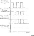
Figure 5 shows simulated voltage profiles at certain positions in the I/O receiver shown inFigure 2 and also in the existing I/O receiver shown inFigure 1 . - Referring to
Figure 5 andFigures 1-2 , the simulations are performed by using 1.6 V for the first power supply voltage VDD1 and 3 V for the high voltage level of the external voltage signal. In addition, a threshold voltage (i.e. Vthn) of 0.9 V is assumed for both the NMOS transistor M31 in the existing I/O receiver and the NMOS transistor N1 in the disclosed I/O receiver. - Referring to
Figure 5 , for the existing I/O receiver shown inFigure 1 , the output voltage of the NMOS transistor M31, i.e. the voltage signal at Node B, may be in a range between 0 V and 0.7 V. That is, the maximum voltage level at Node B may only reach VDD1-Vthn. In such a case, the I/O receiver may still work, but the performance of the I/O receiver may be degraded. For the I/O receiver shown inFigure 2 , the voltage signal at Node B may be in a range between 0 V and 1.6 V. That is, the maximum voltage level at Node B may reach the first power supply voltage VDD1. Therefore, the performance of the I/O receiver may be desired and the working condition of the reformation unit may also be optimized. Therefore, according to the present disclosure, by raising the high voltage level output of the first NMOS transistor N1 to the first power supply voltage VDD1 through a compensation unit, the performance of the I/O receiver may be improved while the complexity of the circuit structure may not be increased. - Compared to existing I/O receivers, the disclosed I/O receivers may demonstrate the following advantages.
- According to the present disclosure, each I/O receiver consistent with the disclosed embodiments may include a receiving terminal, a first NMOS transistor, a reformation circuit, and a compensation unit. The receiving terminal may be coupled with an external voltage signal. The source electrode of the first NMOS transistor may be coupled with the receiving terminal while the gate electrode of the first NMOS transistor may be coupled with a first power supply voltage. The input terminals of the reformation circuit may be coupled with the first power supply voltage, the ground, and the drain electrode of the first NMOS transistor, respectively. The reformation circuit may be used to reform the voltage signal transmitted from the drain electrode of the first NMOS transistor.
- Moreover, according to an I/O receiver consistent with the disclosed embodiments, the compensation unit may further include a first PMOS transistor, a second PMOS transistor, and a second NMOS transistor. Specifically, the source electrode of the first PMOS transistor may be coupled with the first power supply voltage, the drain electrode of the first PMOS transistor may be coupled with the drain electrode of the second NMOS transistor, and the gate electrode of the first PMOS transistor may be coupled with the receiving terminal. The gate electrode of the second NMOS transistor may be coupled with the drain electrode of the first NMOS transistor and the source electrode of the second NMOS transistor may be grounded. Moreover, the source electrode of the second PMOS transistor may be coupled with the first power supply voltage, the gate electrode of the second PMOS transistor may be coupled with the drain electrode of the first PMOS transistor, and the drain electrode of the second PMOS transistor may be coupled with the drain electrode of the first NMOS transistor.
- Further, when the receiving terminal receives a high voltage level signal, the first PMOS transistor may be turned off while the second NMOS transistor may be turned on. Therefore, the voltage level at the drain electrode of the first PMOS transistor may be pulled down through the second NMOS transistor. Moreover, because the drain electrode of the first PMOS transistor may be coupled with the gate electrode of the second PMOS transistor, the second PMOS transistor may then be turned on. Since the drain electrode of the second PMOS transistor may be coupled with the drain electrode of the first NMOS transistor, the voltage at the drain electrode of the first NMOS transistor may reach the operation power supply voltage of the I/O receiver. That is, the compensation unit may provide a compensation voltage to the voltage signal at the drain electrode of the first NMOS transistor such that the maximum level of the voltage signal at the drain electrode of the first NMOS transistor may reach the first power supply voltage. Therefore, with a simple circuit structure, the disclosed I/O receiver accepts external high voltage inputs and also improves the speed and performance of the I/O circuit.
Claims (12)
- An input-output, I/O, receiver, comprising:a receiving terminal, coupled with an external voltage signal;a first NMOS transistor (N1), having a source electrode coupled with the receiving terminal and a gate electrode coupled with a first power supply voltage (VDD1);a reformation circuit (202), configured to sharpen the rising edge and the falling edge of a voltage signal transmitted from a drain electrode of the first NMOS transistor (N1); anda compensation unit (201), including a first PMOS transistor (P1), a second PMOS transistor (P2), a second NMOS transistor (N2) and a third NMOS transistor (N3), the compensation unit (201) configured to provide a compensation voltage to a voltage signal at the drain electrode of the first NMOS transistor (N1), whereby a maximum level of the voltage signal at the drain electrode of the first NMOS transistor (N1) reaches the first power supply voltage (VDD1); wherein:a source electrode of the first PMOS transistor (P1) is coupled with the first power supply voltage (VDD1) and a gate electrode of the first PMOS transistor (P1) is coupled with the receiving terminal;a drain electrode of the second NMOS transistor (N2) is coupled with a drain electrode of the first PMOS transistor (P1), a gate electrode of the second NMOS transistor (N2) is coupled with the drain electrode of the first NMOS transistor (N1), and a source electrode of the second NMOS transistor (N2) is connected to ground; anda drain electrode of the third NMOS transistor (N3) is coupled with the drain electrode of the second PMOS transistor (P2) and the drain electrode of the first NMOS transistor (N1), a gate electrode of the third NMOS transistor (N3) is coupled with the drain electrode of the first PMOS transistor (P1), and a source electrode of the third NMOS transistor (N3) is grounded.
- The I/O receiver according to claim 1, wherein:
a source electrode of the second PMOS transistor (P2) is coupled with the first power supply voltage (VDD1), a gate electrode of the second PMOS transistor (P2) is coupled with the drain electrode of the first PMOS transistor (P1), and a drain electrode of the second PMOS transistor (P2) is coupled with the drain electrode of the first NMOS transistor (N1). - The I/O receiver according to claim 2,
wherein when the external voltage signal increases from a logic-low voltage level to a logic-high voltage level: the first PMOS transistor (P1) is turned off; the second NMOS transistor (N2) is turned on; a voltage level at the drain electrode of the first PMOS transistor (P1) is pulled down through the second NMOS transistor (N2); and when the voltage level at the drain electrode of the first PMOS transistor (P1) becomes less than or equal to a threshold voltage of the second PMOS transistor (P2), the second PMOS transistor (P2) is turned on to let the output voltage level at the drain electrode of the first NMOS transistor (N1) reach the first power supply voltage (VDD1); and/or
wherein when the external voltage signal decreases from a logic-high voltage level to a logic-low voltage level: the first PMOS transistor (P1) is turned on; the second NMOS transistor (N2) is turned off; the voltage level at the drain electrode of the first PMOS transistor (P1) increases; and when the voltage level at the drain electrode of the first PMOS transistor (P1) becomes higher than the threshold voltage of the second PMOS transistor (P2), the second PMOS transistor (P2) is turned off to let the output voltage level at the drain electrode of the first NMOS transistor (N1) drop to the logic-low voltage level. - The I/O receiver according to claim 1,
wherein when the external voltage signal increases from a logic-low voltage level to a logic-high voltage level: the first PMOS transistor (P1) is turned off; the second NMOS transistor (N2) is turned on; a voltage level at the drain electrode of the first PMOS transistor (P1) is pulled down through the second NMOS transistor (N2); and when the voltage level at the drain electrode of the first PMOS transistor (P1) becomes less than or equal to a threshold voltage of the second PMOS transistor (P2), the second PMOS transistor (P2) is turned on and the third NMOS transistor (N3) is turned off to let the output voltage level at the drain electrode of the first NMOS transistor (N1) reach the first power supply voltage (VDD1); and/or
wherein when the external voltage signal decreases from a logic-high voltage level to a logic-low voltage level: the first PMOS transistor (P1) is turned on; the second NMOS transistor (N2) is turned off; the voltage level at the drain electrode of the first PMOS transistor (P1) increases; and when the voltage level at the drain electrode of the first PMOS transistor (P1) becomes higher than the threshold voltage of the second PMOS transistor (P2), the second PMOS transistor (P2) is turned off and the third NMOS transistor (N3) is turned on to let the output voltage level at the drain electrode of the first NMOS transistor (N1) drop to the logic-low voltage level. - The I/O receiver according to claim 1, wherein the reformation circuit (202) is an inverter unit.
- The I/O receiver according to claim 5, wherein:the inverter unit includes a third PMOS transistor (P3) and a fourth NMOS transistor (N4);a source electrode of the third PMOS transistor (P3) is coupled with the first power supply voltage (VDD1) while a gate electrode of the third PMOS transistor (P3) is coupled with the drain electrode of the first NMOS transistor (N1); anda drain electrode of the fourth NMOS transistor (N4) is coupled with the drain electrode of the third PMOS transistor (P3), a source electrode of the fourth NMOS transistor (N4) is grounded, and a gate electrode of the fourth NMOS transistor (N4) is coupled with the drain electrode of the first NMOS transistor (N1).
- The I/O receiver according to claim 6,
wherein when the external voltage signal increase from a logic-low voltage level to a logic-high voltage level: the third PMOS transistor (P3) of the inverter unit is turned off; the fourth NMOS transistor (N4) of the inverter unit is turned on; and the ground pulls down an output voltage of the inverter unit to a logic-low voltage level; and/or
wherein when the external voltage signal decreases from a logic-high voltage level to a logic-low voltage level: the third PMOS transistor (P3) of the inverter unit is turned on; the fourth NMOS transistor (N4) of the inverter unit is turned off; and the first power supply voltage (VDD1) drives an output voltage of the inverter unit to a logic-high voltage level. - The I/O receiver according to claim 5, wherein:the inverter unit includes a third PMOS transistor (P3), a fourth PMOS transistor, a fourth NMOS transistor (N4), and a fifth NMOS transistor;a source electrode of the third PMOS transistor (P3) is coupled with the first power supply voltage (VDD1) while a gate electrode of the third PMOS transistor (P3) is coupled with the drain electrode of the first NMOS transistor (N1);a source electrode of the fourth PMOS transistor is coupled with a drain electrode of the third PMOS transistor (P3) while a gate electrode of the fourth PMOS transistor is coupled with the drain electrode of the first NMOS transistor (N1);a drain electrode of the fourth NMOS transistor (N4) is coupled with a drain electrode of the fourth PMOS transistor while a gate electrode of the fourth NMOS transistor (N4) is coupled with the drain electrode of the first NMOS transistor (N1); anda drain electrode of the fifth NMOS transistor is coupled with a source electrode of the fourth NMOS transistor (N4), a source electrode of the fifth NMOS transistor is grounded, and a gate electrode of the fourth NMOS transistor (N4) is coupled with the drain electrode of the first NMOS transistor (N1).
- The I/O receiver according to claim 8,
wherein when the external voltage signal increases from a logic-low voltage level to a logic-high voltage level: the third PMOS transistor (P3) and the fourth PMOS transistor of the inverter unit are turned off; the fourth NMOS transistor (N4) and the fifth NMOS transistor of the inverter unit is turned on; and the ground pulls down an output voltage of the inverter unit to a logic-low voltage level; and/or
wherein when the external voltage signal decreases from a logic-high voltage level to a logic-low voltage level: the third PMOS transistor (P3) and the fourth PMOS transistor of the inverter unit is turned on; the fourth NMOS transistor (N4) and the fifth NMOS transistor of the inverter unit is turned off; and the first power supply voltage (VDD1) drives an output voltage of the inverter unit to a logic-high voltage level. - The I/O receiver according to any one of the claims 1-9, wherein the reformation circuit (202) has an input terminal coupled with the first power supply voltage (VDD1) and the drain electrode of the first NMOS transistor (N1).
- The I/O receiver according to any one of the claims 1-10, wherein the reformation circuit (202) is a Schmitt trigger.
- The I/O receiver according to any one of the claims 1-11, further including:
a voltage-level converting unit (203), configured to convert a voltage level of an output signal of the reformation circuit (202), wherein:an input terminal of the voltage-level converting unit (203) is coupled with an output terminal of the reformation circuit (202) and a second power supply voltage; andan output terminal of the voltage-level converting unit (203) serves as an output terminal of the I/O receiver.
Applications Claiming Priority (1)
| Application Number | Priority Date | Filing Date | Title |
|---|---|---|---|
| CN201610134366.7A CN107181482B (en) | 2016-03-09 | 2016-03-09 | Input/output receiving circuit |
Publications (2)
| Publication Number | Publication Date |
|---|---|
| EP3217552A1 EP3217552A1 (en) | 2017-09-13 |
| EP3217552B1 true EP3217552B1 (en) | 2020-04-29 |
Family
ID=58261500
Family Applications (1)
| Application Number | Title | Priority Date | Filing Date |
|---|---|---|---|
| EP17158753.8A Active EP3217552B1 (en) | 2016-03-09 | 2017-03-01 | Input-output receiver |
Country Status (3)
| Country | Link |
|---|---|
| US (1) | US10243564B2 (en) |
| EP (1) | EP3217552B1 (en) |
| CN (1) | CN107181482B (en) |
Families Citing this family (9)
| Publication number | Priority date | Publication date | Assignee | Title |
|---|---|---|---|---|
| CN107526700B (en) * | 2016-06-22 | 2021-06-22 | 中芯国际集成电路制造(上海)有限公司 | Input/output receiving circuit and electronic device |
| CN107528580B (en) * | 2017-09-22 | 2020-09-08 | 上海安其威微电子科技有限公司 | Level shift circuit |
| US10965261B2 (en) | 2017-12-05 | 2021-03-30 | Qualcomm Incorporated | Power amplifier circuit |
| CN109787607B (en) * | 2019-01-10 | 2023-05-26 | 苏州睿晟芯微电子科技有限公司 | High-voltage high-speed IO circuit based on low-voltage device |
| CN110048711B (en) * | 2019-05-15 | 2023-11-21 | 苏州锴威特半导体股份有限公司 | Digital signal processing circuit for resisting ground and power supply rebound noise |
| CN111835373B (en) * | 2019-11-18 | 2023-11-14 | 紫光同芯微电子有限公司 | Novel SWP interface circuit |
| CN114793114B (en) * | 2021-01-26 | 2025-03-11 | 深圳比特微电子科技有限公司 | Compound logic gate circuits and computing devices |
| CN114189136B (en) * | 2021-11-25 | 2024-02-06 | 上海华虹宏力半导体制造有限公司 | Discharge circuit |
| CN119051634B (en) * | 2024-10-29 | 2025-04-25 | 中科芯集成电路有限公司 | Edge delay circuit with anti-shake function |
Family Cites Families (12)
| Publication number | Priority date | Publication date | Assignee | Title |
|---|---|---|---|---|
| JPS5990292A (en) * | 1982-11-12 | 1984-05-24 | Toshiba Corp | Voltage converting circuit |
| JP2567179B2 (en) | 1992-03-18 | 1996-12-25 | 株式会社東芝 | Level conversion circuit |
| JP2658867B2 (en) * | 1994-02-18 | 1997-09-30 | 日本電気株式会社 | Level conversion circuit |
| WO1996042139A1 (en) * | 1995-06-13 | 1996-12-27 | Advanced Micro Devices, Inc. | Input receiver, output driver, and input/output driver circuits capable of high voltage operation for an integrated circuit |
| US6031393A (en) * | 1997-12-31 | 2000-02-29 | Intel Corporation | Pass gate input buffer for a mixed voltage environment |
| US7504861B2 (en) * | 2003-11-20 | 2009-03-17 | Transpacific Ip, Ltd. | Input stage for mixed-voltage-tolerant buffer with reduced leakage |
| US8593203B2 (en) * | 2008-07-29 | 2013-11-26 | Qualcomm Incorporated | High signal level compliant input/output circuits |
| US8106699B2 (en) * | 2008-07-29 | 2012-01-31 | Qualcomm Incorporated | High signal level compliant input/output circuits |
| CN101753129B (en) * | 2008-12-01 | 2011-11-30 | 中芯国际集成电路制造(上海)有限公司 | High-voltage tolerance output buffer |
| CN103905028B (en) * | 2012-12-25 | 2018-05-25 | 中芯国际集成电路制造(上海)有限公司 | Signal receiver and signal transmission apparatus |
| CN104158534B (en) * | 2013-05-14 | 2017-06-23 | 中芯国际集成电路制造(上海)有限公司 | For the decompression converting circuit of I/O interfaces |
| KR102242582B1 (en) * | 2014-10-10 | 2021-04-22 | 삼성전자주식회사 | Receiver circuit and signal receiving method thereof |
-
2016
- 2016-03-09 CN CN201610134366.7A patent/CN107181482B/en active Active
-
2017
- 2017-02-20 US US15/436,911 patent/US10243564B2/en active Active
- 2017-03-01 EP EP17158753.8A patent/EP3217552B1/en active Active
Non-Patent Citations (1)
| Title |
|---|
| None * |
Also Published As
| Publication number | Publication date |
|---|---|
| EP3217552A1 (en) | 2017-09-13 |
| US10243564B2 (en) | 2019-03-26 |
| CN107181482B (en) | 2020-09-08 |
| CN107181482A (en) | 2017-09-19 |
| US20170264297A1 (en) | 2017-09-14 |
Similar Documents
| Publication | Publication Date | Title |
|---|---|---|
| EP3217552B1 (en) | Input-output receiver | |
| US8779739B2 (en) | Integrated DC converter with improved driving stage | |
| US20050017755A1 (en) | Low-to-high level shifter | |
| US20130181762A1 (en) | Current mirror modified level shifter | |
| US6791391B2 (en) | Level shifting circuit | |
| US7868659B2 (en) | I/O buffer with twice the supply voltage tolerance using normal supply voltage devices | |
| KR102739994B1 (en) | Apparatus and method for reducing output skew and transition delay of level shifter | |
| CN103856205A (en) | Level switching circuit, drive circuit for driving high voltage devices and corresponding method | |
| US7446564B2 (en) | Level shifter | |
| CN104052454A (en) | Level shifter for high density integrated circuits | |
| CN112243569B (en) | Semiconductor integrated circuit device | |
| EP2143206B1 (en) | Electronic device with a high voltage tolerant unit | |
| US10135442B2 (en) | Current-mode logic circuit | |
| US10305481B2 (en) | Pre-driver for driving low voltage differential signaling (LVDS) driving circuit | |
| CN107181481B (en) | Input/output receiving circuit | |
| US10482966B2 (en) | Block decoder of nonvolatile memory and level shifter | |
| JP2006033825A (en) | Level shifter and level shifting method | |
| CN108712166B (en) | Self-adaptive level conversion circuit | |
| CN114389595B (en) | Level conversion circuit | |
| US9935636B1 (en) | CMOS input buffer with low supply current and voltage down shifting | |
| CN101459424B (en) | Output Units, Input Units, and I/O Elements | |
| US12323141B2 (en) | Level shifter | |
| US8570091B2 (en) | Level shifter | |
| WO2018193724A1 (en) | Output circuit | |
| US8502559B2 (en) | Level translator |
Legal Events
| Date | Code | Title | Description |
|---|---|---|---|
| PUAI | Public reference made under article 153(3) epc to a published international application that has entered the european phase |
Free format text: ORIGINAL CODE: 0009012 |
|
| STAA | Information on the status of an ep patent application or granted ep patent |
Free format text: STATUS: THE APPLICATION HAS BEEN PUBLISHED |
|
| AK | Designated contracting states |
Kind code of ref document: A1 Designated state(s): AL AT BE BG CH CY CZ DE DK EE ES FI FR GB GR HR HU IE IS IT LI LT LU LV MC MK MT NL NO PL PT RO RS SE SI SK SM TR |
|
| AX | Request for extension of the european patent |
Extension state: BA ME |
|
| STAA | Information on the status of an ep patent application or granted ep patent |
Free format text: STATUS: REQUEST FOR EXAMINATION WAS MADE |
|
| 17P | Request for examination filed |
Effective date: 20171106 |
|
| RBV | Designated contracting states (corrected) |
Designated state(s): AL AT BE BG CH CY CZ DE DK EE ES FI FR GB GR HR HU IE IS IT LI LT LU LV MC MK MT NL NO PL PT RO RS SE SI SK SM TR |
|
| STAA | Information on the status of an ep patent application or granted ep patent |
Free format text: STATUS: EXAMINATION IS IN PROGRESS |
|
| RAP1 | Party data changed (applicant data changed or rights of an application transferred) |
Owner name: SEMICONDUCTOR MANUFACTURING INTERNATIONAL (SHANGHA Owner name: SEMICONDUCTOR MANUFACTURING INTERNATIONAL (BEIJING |
|
| 17Q | First examination report despatched |
Effective date: 20181029 |
|
| GRAP | Despatch of communication of intention to grant a patent |
Free format text: ORIGINAL CODE: EPIDOSNIGR1 |
|
| STAA | Information on the status of an ep patent application or granted ep patent |
Free format text: STATUS: GRANT OF PATENT IS INTENDED |
|
| INTG | Intention to grant announced |
Effective date: 20191028 |
|
| GRAS | Grant fee paid |
Free format text: ORIGINAL CODE: EPIDOSNIGR3 |
|
| GRAA | (expected) grant |
Free format text: ORIGINAL CODE: 0009210 |
|
| STAA | Information on the status of an ep patent application or granted ep patent |
Free format text: STATUS: THE PATENT HAS BEEN GRANTED |
|
| AK | Designated contracting states |
Kind code of ref document: B1 Designated state(s): AL AT BE BG CH CY CZ DE DK EE ES FI FR GB GR HR HU IE IS IT LI LT LU LV MC MK MT NL NO PL PT RO RS SE SI SK SM TR |
|
| REG | Reference to a national code |
Ref country code: GB Ref legal event code: FG4D |
|
| REG | Reference to a national code |
Ref country code: CH Ref legal event code: EP |
|
| REG | Reference to a national code |
Ref country code: AT Ref legal event code: REF Ref document number: 1264847 Country of ref document: AT Kind code of ref document: T Effective date: 20200515 |
|
| REG | Reference to a national code |
Ref country code: DE Ref legal event code: R096 Ref document number: 602017015465 Country of ref document: DE |
|
| REG | Reference to a national code |
Ref country code: IE Ref legal event code: FG4D |
|
| REG | Reference to a national code |
Ref country code: NL Ref legal event code: MP Effective date: 20200429 |
|
| REG | Reference to a national code |
Ref country code: LT Ref legal event code: MG4D |
|
| PG25 | Lapsed in a contracting state [announced via postgrant information from national office to epo] |
Ref country code: LT Free format text: LAPSE BECAUSE OF FAILURE TO SUBMIT A TRANSLATION OF THE DESCRIPTION OR TO PAY THE FEE WITHIN THE PRESCRIBED TIME-LIMIT Effective date: 20200429 Ref country code: NO Free format text: LAPSE BECAUSE OF FAILURE TO SUBMIT A TRANSLATION OF THE DESCRIPTION OR TO PAY THE FEE WITHIN THE PRESCRIBED TIME-LIMIT Effective date: 20200729 Ref country code: SE Free format text: LAPSE BECAUSE OF FAILURE TO SUBMIT A TRANSLATION OF THE DESCRIPTION OR TO PAY THE FEE WITHIN THE PRESCRIBED TIME-LIMIT Effective date: 20200429 Ref country code: IS Free format text: LAPSE BECAUSE OF FAILURE TO SUBMIT A TRANSLATION OF THE DESCRIPTION OR TO PAY THE FEE WITHIN THE PRESCRIBED TIME-LIMIT Effective date: 20200829 Ref country code: FI Free format text: LAPSE BECAUSE OF FAILURE TO SUBMIT A TRANSLATION OF THE DESCRIPTION OR TO PAY THE FEE WITHIN THE PRESCRIBED TIME-LIMIT Effective date: 20200429 Ref country code: PT Free format text: LAPSE BECAUSE OF FAILURE TO SUBMIT A TRANSLATION OF THE DESCRIPTION OR TO PAY THE FEE WITHIN THE PRESCRIBED TIME-LIMIT Effective date: 20200831 Ref country code: GR Free format text: LAPSE BECAUSE OF FAILURE TO SUBMIT A TRANSLATION OF THE DESCRIPTION OR TO PAY THE FEE WITHIN THE PRESCRIBED TIME-LIMIT Effective date: 20200730 |
|
| REG | Reference to a national code |
Ref country code: AT Ref legal event code: MK05 Ref document number: 1264847 Country of ref document: AT Kind code of ref document: T Effective date: 20200429 |
|
| PG25 | Lapsed in a contracting state [announced via postgrant information from national office to epo] |
Ref country code: RS Free format text: LAPSE BECAUSE OF FAILURE TO SUBMIT A TRANSLATION OF THE DESCRIPTION OR TO PAY THE FEE WITHIN THE PRESCRIBED TIME-LIMIT Effective date: 20200429 Ref country code: LV Free format text: LAPSE BECAUSE OF FAILURE TO SUBMIT A TRANSLATION OF THE DESCRIPTION OR TO PAY THE FEE WITHIN THE PRESCRIBED TIME-LIMIT Effective date: 20200429 Ref country code: HR Free format text: LAPSE BECAUSE OF FAILURE TO SUBMIT A TRANSLATION OF THE DESCRIPTION OR TO PAY THE FEE WITHIN THE PRESCRIBED TIME-LIMIT Effective date: 20200429 Ref country code: BG Free format text: LAPSE BECAUSE OF FAILURE TO SUBMIT A TRANSLATION OF THE DESCRIPTION OR TO PAY THE FEE WITHIN THE PRESCRIBED TIME-LIMIT Effective date: 20200729 |
|
| PG25 | Lapsed in a contracting state [announced via postgrant information from national office to epo] |
Ref country code: NL Free format text: LAPSE BECAUSE OF FAILURE TO SUBMIT A TRANSLATION OF THE DESCRIPTION OR TO PAY THE FEE WITHIN THE PRESCRIBED TIME-LIMIT Effective date: 20200429 Ref country code: AL Free format text: LAPSE BECAUSE OF FAILURE TO SUBMIT A TRANSLATION OF THE DESCRIPTION OR TO PAY THE FEE WITHIN THE PRESCRIBED TIME-LIMIT Effective date: 20200429 |
|
| PG25 | Lapsed in a contracting state [announced via postgrant information from national office to epo] |
Ref country code: CZ Free format text: LAPSE BECAUSE OF FAILURE TO SUBMIT A TRANSLATION OF THE DESCRIPTION OR TO PAY THE FEE WITHIN THE PRESCRIBED TIME-LIMIT Effective date: 20200429 Ref country code: IT Free format text: LAPSE BECAUSE OF FAILURE TO SUBMIT A TRANSLATION OF THE DESCRIPTION OR TO PAY THE FEE WITHIN THE PRESCRIBED TIME-LIMIT Effective date: 20200429 Ref country code: DK Free format text: LAPSE BECAUSE OF FAILURE TO SUBMIT A TRANSLATION OF THE DESCRIPTION OR TO PAY THE FEE WITHIN THE PRESCRIBED TIME-LIMIT Effective date: 20200429 Ref country code: EE Free format text: LAPSE BECAUSE OF FAILURE TO SUBMIT A TRANSLATION OF THE DESCRIPTION OR TO PAY THE FEE WITHIN THE PRESCRIBED TIME-LIMIT Effective date: 20200429 Ref country code: SM Free format text: LAPSE BECAUSE OF FAILURE TO SUBMIT A TRANSLATION OF THE DESCRIPTION OR TO PAY THE FEE WITHIN THE PRESCRIBED TIME-LIMIT Effective date: 20200429 Ref country code: AT Free format text: LAPSE BECAUSE OF FAILURE TO SUBMIT A TRANSLATION OF THE DESCRIPTION OR TO PAY THE FEE WITHIN THE PRESCRIBED TIME-LIMIT Effective date: 20200429 Ref country code: RO Free format text: LAPSE BECAUSE OF FAILURE TO SUBMIT A TRANSLATION OF THE DESCRIPTION OR TO PAY THE FEE WITHIN THE PRESCRIBED TIME-LIMIT Effective date: 20200429 Ref country code: ES Free format text: LAPSE BECAUSE OF FAILURE TO SUBMIT A TRANSLATION OF THE DESCRIPTION OR TO PAY THE FEE WITHIN THE PRESCRIBED TIME-LIMIT Effective date: 20200429 |
|
| REG | Reference to a national code |
Ref country code: DE Ref legal event code: R097 Ref document number: 602017015465 Country of ref document: DE |
|
| PG25 | Lapsed in a contracting state [announced via postgrant information from national office to epo] |
Ref country code: SK Free format text: LAPSE BECAUSE OF FAILURE TO SUBMIT A TRANSLATION OF THE DESCRIPTION OR TO PAY THE FEE WITHIN THE PRESCRIBED TIME-LIMIT Effective date: 20200429 Ref country code: PL Free format text: LAPSE BECAUSE OF FAILURE TO SUBMIT A TRANSLATION OF THE DESCRIPTION OR TO PAY THE FEE WITHIN THE PRESCRIBED TIME-LIMIT Effective date: 20200429 |
|
| PLBE | No opposition filed within time limit |
Free format text: ORIGINAL CODE: 0009261 |
|
| STAA | Information on the status of an ep patent application or granted ep patent |
Free format text: STATUS: NO OPPOSITION FILED WITHIN TIME LIMIT |
|
| 26N | No opposition filed |
Effective date: 20210201 |
|
| PG25 | Lapsed in a contracting state [announced via postgrant information from national office to epo] |
Ref country code: SI Free format text: LAPSE BECAUSE OF FAILURE TO SUBMIT A TRANSLATION OF THE DESCRIPTION OR TO PAY THE FEE WITHIN THE PRESCRIBED TIME-LIMIT Effective date: 20200429 |
|
| PG25 | Lapsed in a contracting state [announced via postgrant information from national office to epo] |
Ref country code: MC Free format text: LAPSE BECAUSE OF FAILURE TO SUBMIT A TRANSLATION OF THE DESCRIPTION OR TO PAY THE FEE WITHIN THE PRESCRIBED TIME-LIMIT Effective date: 20200429 |
|
| REG | Reference to a national code |
Ref country code: CH Ref legal event code: PL |
|
| GBPC | Gb: european patent ceased through non-payment of renewal fee |
Effective date: 20210301 |
|
| REG | Reference to a national code |
Ref country code: BE Ref legal event code: MM Effective date: 20210331 |
|
| PG25 | Lapsed in a contracting state [announced via postgrant information from national office to epo] |
Ref country code: LU Free format text: LAPSE BECAUSE OF NON-PAYMENT OF DUE FEES Effective date: 20210301 Ref country code: LI Free format text: LAPSE BECAUSE OF NON-PAYMENT OF DUE FEES Effective date: 20210331 Ref country code: CH Free format text: LAPSE BECAUSE OF NON-PAYMENT OF DUE FEES Effective date: 20210331 Ref country code: FR Free format text: LAPSE BECAUSE OF NON-PAYMENT OF DUE FEES Effective date: 20210331 Ref country code: IE Free format text: LAPSE BECAUSE OF NON-PAYMENT OF DUE FEES Effective date: 20210301 Ref country code: GB Free format text: LAPSE BECAUSE OF NON-PAYMENT OF DUE FEES Effective date: 20210301 |
|
| PG25 | Lapsed in a contracting state [announced via postgrant information from national office to epo] |
Ref country code: BE Free format text: LAPSE BECAUSE OF NON-PAYMENT OF DUE FEES Effective date: 20210331 |
|
| PG25 | Lapsed in a contracting state [announced via postgrant information from national office to epo] |
Ref country code: HU Free format text: LAPSE BECAUSE OF FAILURE TO SUBMIT A TRANSLATION OF THE DESCRIPTION OR TO PAY THE FEE WITHIN THE PRESCRIBED TIME-LIMIT; INVALID AB INITIO Effective date: 20170301 |
|
| PG25 | Lapsed in a contracting state [announced via postgrant information from national office to epo] |
Ref country code: CY Free format text: LAPSE BECAUSE OF FAILURE TO SUBMIT A TRANSLATION OF THE DESCRIPTION OR TO PAY THE FEE WITHIN THE PRESCRIBED TIME-LIMIT Effective date: 20200429 |
|
| PG25 | Lapsed in a contracting state [announced via postgrant information from national office to epo] |
Ref country code: MK Free format text: LAPSE BECAUSE OF FAILURE TO SUBMIT A TRANSLATION OF THE DESCRIPTION OR TO PAY THE FEE WITHIN THE PRESCRIBED TIME-LIMIT Effective date: 20200429 |
|
| PG25 | Lapsed in a contracting state [announced via postgrant information from national office to epo] |
Ref country code: MT Free format text: LAPSE BECAUSE OF FAILURE TO SUBMIT A TRANSLATION OF THE DESCRIPTION OR TO PAY THE FEE WITHIN THE PRESCRIBED TIME-LIMIT Effective date: 20200429 |
|
| PG25 | Lapsed in a contracting state [announced via postgrant information from national office to epo] |
Ref country code: TR Free format text: LAPSE BECAUSE OF FAILURE TO SUBMIT A TRANSLATION OF THE DESCRIPTION OR TO PAY THE FEE WITHIN THE PRESCRIBED TIME-LIMIT Effective date: 20200429 |
|
| PGFP | Annual fee paid to national office [announced via postgrant information from national office to epo] |
Ref country code: DE Payment date: 20260319 Year of fee payment: 10 |