EP3204686B1 - Verbindungseinheit für eine direktionale rückbeleuchtung - Google Patents
Verbindungseinheit für eine direktionale rückbeleuchtung Download PDFInfo
- Publication number
- EP3204686B1 EP3204686B1 EP15848224.0A EP15848224A EP3204686B1 EP 3204686 B1 EP3204686 B1 EP 3204686B1 EP 15848224 A EP15848224 A EP 15848224A EP 3204686 B1 EP3204686 B1 EP 3204686B1
- Authority
- EP
- European Patent Office
- Prior art keywords
- light
- base portion
- waveguide
- mounting strip
- end portion
- Prior art date
- Legal status (The legal status is an assumption and is not a legal conclusion. Google has not performed a legal analysis and makes no representation as to the accuracy of the status listed.)
- Active
Links
- 230000003287 optical effect Effects 0.000 claims description 52
- 239000000615 nonconductor Substances 0.000 claims description 17
- 229910052751 metal Inorganic materials 0.000 claims description 9
- 239000002184 metal Substances 0.000 claims description 9
- RYGMFSIKBFXOCR-UHFFFAOYSA-N Copper Chemical compound [Cu] RYGMFSIKBFXOCR-UHFFFAOYSA-N 0.000 claims description 6
- 239000010949 copper Substances 0.000 claims description 6
- 229910052802 copper Inorganic materials 0.000 claims description 6
- 238000010586 diagram Methods 0.000 description 54
- 238000003384 imaging method Methods 0.000 description 48
- 239000010410 layer Substances 0.000 description 47
- 238000005286 illumination Methods 0.000 description 29
- 238000000605 extraction Methods 0.000 description 24
- 238000009826 distribution Methods 0.000 description 14
- 229910000679 solder Inorganic materials 0.000 description 10
- 238000000034 method Methods 0.000 description 8
- 239000012212 insulator Substances 0.000 description 6
- 238000003491 array Methods 0.000 description 5
- 238000010276 construction Methods 0.000 description 4
- 238000005259 measurement Methods 0.000 description 4
- 230000001902 propagating effect Effects 0.000 description 4
- BQCADISMDOOEFD-UHFFFAOYSA-N Silver Chemical compound [Ag] BQCADISMDOOEFD-UHFFFAOYSA-N 0.000 description 3
- 238000013461 design Methods 0.000 description 3
- 230000006870 function Effects 0.000 description 3
- 210000003128 head Anatomy 0.000 description 3
- 239000004973 liquid crystal related substance Substances 0.000 description 3
- 239000000463 material Substances 0.000 description 3
- 229910052709 silver Inorganic materials 0.000 description 3
- 239000004332 silver Substances 0.000 description 3
- 230000000007 visual effect Effects 0.000 description 3
- 229910052782 aluminium Inorganic materials 0.000 description 2
- XAGFODPZIPBFFR-UHFFFAOYSA-N aluminium Chemical compound [Al] XAGFODPZIPBFFR-UHFFFAOYSA-N 0.000 description 2
- 230000000712 assembly Effects 0.000 description 2
- 238000000429 assembly Methods 0.000 description 2
- 230000001419 dependent effect Effects 0.000 description 2
- 239000002355 dual-layer Substances 0.000 description 2
- 230000000694 effects Effects 0.000 description 2
- 238000005516 engineering process Methods 0.000 description 2
- 210000000887 face Anatomy 0.000 description 2
- 230000004044 response Effects 0.000 description 2
- 239000004065 semiconductor Substances 0.000 description 2
- 239000000758 substrate Substances 0.000 description 2
- 239000004411 aluminium Substances 0.000 description 1
- 230000008859 change Effects 0.000 description 1
- 238000012512 characterization method Methods 0.000 description 1
- 239000004020 conductor Substances 0.000 description 1
- 230000003247 decreasing effect Effects 0.000 description 1
- 230000009977 dual effect Effects 0.000 description 1
- -1 for example Substances 0.000 description 1
- 238000010438 heat treatment Methods 0.000 description 1
- 238000007373 indentation Methods 0.000 description 1
- 238000009413 insulation Methods 0.000 description 1
- 230000013011 mating Effects 0.000 description 1
- 238000012986 modification Methods 0.000 description 1
- 230000004048 modification Effects 0.000 description 1
- 230000002093 peripheral effect Effects 0.000 description 1
- 229920000728 polyester Polymers 0.000 description 1
- 230000008569 process Effects 0.000 description 1
- 238000012545 processing Methods 0.000 description 1
- 230000009467 reduction Effects 0.000 description 1
Images


Classifications
-
- G—PHYSICS
- G02—OPTICS
- G02B—OPTICAL ELEMENTS, SYSTEMS OR APPARATUS
- G02B6/00—Light guides; Structural details of arrangements comprising light guides and other optical elements, e.g. couplings
- G02B6/0001—Light guides; Structural details of arrangements comprising light guides and other optical elements, e.g. couplings specially adapted for lighting devices or systems
- G02B6/0011—Light guides; Structural details of arrangements comprising light guides and other optical elements, e.g. couplings specially adapted for lighting devices or systems the light guides being planar or of plate-like form
- G02B6/0081—Mechanical or electrical aspects of the light guide and light source in the lighting device peculiar to the adaptation to planar light guides, e.g. concerning packaging
- G02B6/0083—Details of electrical connections of light sources to drivers, circuit boards, or the like
-
- G—PHYSICS
- G02—OPTICS
- G02B—OPTICAL ELEMENTS, SYSTEMS OR APPARATUS
- G02B6/00—Light guides; Structural details of arrangements comprising light guides and other optical elements, e.g. couplings
- G02B6/0001—Light guides; Structural details of arrangements comprising light guides and other optical elements, e.g. couplings specially adapted for lighting devices or systems
- G02B6/0011—Light guides; Structural details of arrangements comprising light guides and other optical elements, e.g. couplings specially adapted for lighting devices or systems the light guides being planar or of plate-like form
- G02B6/0033—Means for improving the coupling-out of light from the light guide
- G02B6/0035—Means for improving the coupling-out of light from the light guide provided on the surface of the light guide or in the bulk of it
- G02B6/0045—Means for improving the coupling-out of light from the light guide provided on the surface of the light guide or in the bulk of it by shaping at least a portion of the light guide
- G02B6/0046—Tapered light guide, e.g. wedge-shaped light guide
- G02B6/0048—Tapered light guide, e.g. wedge-shaped light guide with stepwise taper
-
- G—PHYSICS
- G02—OPTICS
- G02B—OPTICAL ELEMENTS, SYSTEMS OR APPARATUS
- G02B6/00—Light guides; Structural details of arrangements comprising light guides and other optical elements, e.g. couplings
- G02B6/0001—Light guides; Structural details of arrangements comprising light guides and other optical elements, e.g. couplings specially adapted for lighting devices or systems
- G02B6/0011—Light guides; Structural details of arrangements comprising light guides and other optical elements, e.g. couplings specially adapted for lighting devices or systems the light guides being planar or of plate-like form
- G02B6/0033—Means for improving the coupling-out of light from the light guide
- G02B6/005—Means for improving the coupling-out of light from the light guide provided by one optical element, or plurality thereof, placed on the light output side of the light guide
- G02B6/0055—Reflecting element, sheet or layer
-
- G—PHYSICS
- G02—OPTICS
- G02B—OPTICAL ELEMENTS, SYSTEMS OR APPARATUS
- G02B6/00—Light guides; Structural details of arrangements comprising light guides and other optical elements, e.g. couplings
- G02B6/0001—Light guides; Structural details of arrangements comprising light guides and other optical elements, e.g. couplings specially adapted for lighting devices or systems
- G02B6/0011—Light guides; Structural details of arrangements comprising light guides and other optical elements, e.g. couplings specially adapted for lighting devices or systems the light guides being planar or of plate-like form
- G02B6/0066—Light guides; Structural details of arrangements comprising light guides and other optical elements, e.g. couplings specially adapted for lighting devices or systems the light guides being planar or of plate-like form characterised by the light source being coupled to the light guide
- G02B6/0068—Arrangements of plural sources, e.g. multi-colour light sources
-
- G—PHYSICS
- G02—OPTICS
- G02B—OPTICAL ELEMENTS, SYSTEMS OR APPARATUS
- G02B6/00—Light guides; Structural details of arrangements comprising light guides and other optical elements, e.g. couplings
- G02B6/0001—Light guides; Structural details of arrangements comprising light guides and other optical elements, e.g. couplings specially adapted for lighting devices or systems
- G02B6/0011—Light guides; Structural details of arrangements comprising light guides and other optical elements, e.g. couplings specially adapted for lighting devices or systems the light guides being planar or of plate-like form
- G02B6/0066—Light guides; Structural details of arrangements comprising light guides and other optical elements, e.g. couplings specially adapted for lighting devices or systems the light guides being planar or of plate-like form characterised by the light source being coupled to the light guide
- G02B6/0073—Light emitting diode [LED]
-
- G—PHYSICS
- G02—OPTICS
- G02B—OPTICAL ELEMENTS, SYSTEMS OR APPARATUS
- G02B6/00—Light guides; Structural details of arrangements comprising light guides and other optical elements, e.g. couplings
- G02B6/0001—Light guides; Structural details of arrangements comprising light guides and other optical elements, e.g. couplings specially adapted for lighting devices or systems
- G02B6/0011—Light guides; Structural details of arrangements comprising light guides and other optical elements, e.g. couplings specially adapted for lighting devices or systems the light guides being planar or of plate-like form
- G02B6/0081—Mechanical or electrical aspects of the light guide and light source in the lighting device peculiar to the adaptation to planar light guides, e.g. concerning packaging
- G02B6/0085—Means for removing heat created by the light source from the package
-
- G—PHYSICS
- G02—OPTICS
- G02B—OPTICAL ELEMENTS, SYSTEMS OR APPARATUS
- G02B6/00—Light guides; Structural details of arrangements comprising light guides and other optical elements, e.g. couplings
- G02B6/0001—Light guides; Structural details of arrangements comprising light guides and other optical elements, e.g. couplings specially adapted for lighting devices or systems
- G02B6/0011—Light guides; Structural details of arrangements comprising light guides and other optical elements, e.g. couplings specially adapted for lighting devices or systems the light guides being planar or of plate-like form
- G02B6/0081—Mechanical or electrical aspects of the light guide and light source in the lighting device peculiar to the adaptation to planar light guides, e.g. concerning packaging
- G02B6/0086—Positioning aspects
-
- G—PHYSICS
- G02—OPTICS
- G02F—OPTICAL DEVICES OR ARRANGEMENTS FOR THE CONTROL OF LIGHT BY MODIFICATION OF THE OPTICAL PROPERTIES OF THE MEDIA OF THE ELEMENTS INVOLVED THEREIN; NON-LINEAR OPTICS; FREQUENCY-CHANGING OF LIGHT; OPTICAL LOGIC ELEMENTS; OPTICAL ANALOGUE/DIGITAL CONVERTERS
- G02F1/00—Devices or arrangements for the control of the intensity, colour, phase, polarisation or direction of light arriving from an independent light source, e.g. switching, gating or modulating; Non-linear optics
- G02F1/01—Devices or arrangements for the control of the intensity, colour, phase, polarisation or direction of light arriving from an independent light source, e.g. switching, gating or modulating; Non-linear optics for the control of the intensity, phase, polarisation or colour
- G02F1/13—Devices or arrangements for the control of the intensity, colour, phase, polarisation or direction of light arriving from an independent light source, e.g. switching, gating or modulating; Non-linear optics for the control of the intensity, phase, polarisation or colour based on liquid crystals, e.g. single liquid crystal display cells
- G02F1/1323—Arrangements for providing a switchable viewing angle
-
- G—PHYSICS
- G02—OPTICS
- G02F—OPTICAL DEVICES OR ARRANGEMENTS FOR THE CONTROL OF LIGHT BY MODIFICATION OF THE OPTICAL PROPERTIES OF THE MEDIA OF THE ELEMENTS INVOLVED THEREIN; NON-LINEAR OPTICS; FREQUENCY-CHANGING OF LIGHT; OPTICAL LOGIC ELEMENTS; OPTICAL ANALOGUE/DIGITAL CONVERTERS
- G02F1/00—Devices or arrangements for the control of the intensity, colour, phase, polarisation or direction of light arriving from an independent light source, e.g. switching, gating or modulating; Non-linear optics
- G02F1/01—Devices or arrangements for the control of the intensity, colour, phase, polarisation or direction of light arriving from an independent light source, e.g. switching, gating or modulating; Non-linear optics for the control of the intensity, phase, polarisation or colour
- G02F1/13—Devices or arrangements for the control of the intensity, colour, phase, polarisation or direction of light arriving from an independent light source, e.g. switching, gating or modulating; Non-linear optics for the control of the intensity, phase, polarisation or colour based on liquid crystals, e.g. single liquid crystal display cells
- G02F1/133—Constructional arrangements; Operation of liquid crystal cells; Circuit arrangements
- G02F1/1333—Constructional arrangements; Manufacturing methods
- G02F1/1335—Structural association of cells with optical devices, e.g. polarisers or reflectors
- G02F1/1336—Illuminating devices
- G02F1/133615—Edge-illuminating devices, i.e. illuminating from the side
-
- H—ELECTRICITY
- H01—ELECTRIC ELEMENTS
- H01L—SEMICONDUCTOR DEVICES NOT COVERED BY CLASS H10
- H01L25/00—Assemblies consisting of a plurality of semiconductor or other solid state devices
-
- H—ELECTRICITY
- H05—ELECTRIC TECHNIQUES NOT OTHERWISE PROVIDED FOR
- H05K—PRINTED CIRCUITS; CASINGS OR CONSTRUCTIONAL DETAILS OF ELECTRIC APPARATUS; MANUFACTURE OF ASSEMBLAGES OF ELECTRICAL COMPONENTS
- H05K1/00—Printed circuits
- H05K1/02—Details
- H05K1/03—Use of materials for the substrate
- H05K1/05—Insulated conductive substrates, e.g. insulated metal substrate
-
- G—PHYSICS
- G02—OPTICS
- G02F—OPTICAL DEVICES OR ARRANGEMENTS FOR THE CONTROL OF LIGHT BY MODIFICATION OF THE OPTICAL PROPERTIES OF THE MEDIA OF THE ELEMENTS INVOLVED THEREIN; NON-LINEAR OPTICS; FREQUENCY-CHANGING OF LIGHT; OPTICAL LOGIC ELEMENTS; OPTICAL ANALOGUE/DIGITAL CONVERTERS
- G02F1/00—Devices or arrangements for the control of the intensity, colour, phase, polarisation or direction of light arriving from an independent light source, e.g. switching, gating or modulating; Non-linear optics
- G02F1/01—Devices or arrangements for the control of the intensity, colour, phase, polarisation or direction of light arriving from an independent light source, e.g. switching, gating or modulating; Non-linear optics for the control of the intensity, phase, polarisation or colour
- G02F1/13—Devices or arrangements for the control of the intensity, colour, phase, polarisation or direction of light arriving from an independent light source, e.g. switching, gating or modulating; Non-linear optics for the control of the intensity, phase, polarisation or colour based on liquid crystals, e.g. single liquid crystal display cells
- G02F1/133—Constructional arrangements; Operation of liquid crystal cells; Circuit arrangements
- G02F1/1333—Constructional arrangements; Manufacturing methods
- G02F1/1335—Structural association of cells with optical devices, e.g. polarisers or reflectors
- G02F1/1336—Illuminating devices
- G02F1/133601—Illuminating devices for spatial active dimming
-
- G—PHYSICS
- G02—OPTICS
- G02F—OPTICAL DEVICES OR ARRANGEMENTS FOR THE CONTROL OF LIGHT BY MODIFICATION OF THE OPTICAL PROPERTIES OF THE MEDIA OF THE ELEMENTS INVOLVED THEREIN; NON-LINEAR OPTICS; FREQUENCY-CHANGING OF LIGHT; OPTICAL LOGIC ELEMENTS; OPTICAL ANALOGUE/DIGITAL CONVERTERS
- G02F1/00—Devices or arrangements for the control of the intensity, colour, phase, polarisation or direction of light arriving from an independent light source, e.g. switching, gating or modulating; Non-linear optics
- G02F1/01—Devices or arrangements for the control of the intensity, colour, phase, polarisation or direction of light arriving from an independent light source, e.g. switching, gating or modulating; Non-linear optics for the control of the intensity, phase, polarisation or colour
- G02F1/13—Devices or arrangements for the control of the intensity, colour, phase, polarisation or direction of light arriving from an independent light source, e.g. switching, gating or modulating; Non-linear optics for the control of the intensity, phase, polarisation or colour based on liquid crystals, e.g. single liquid crystal display cells
- G02F1/133—Constructional arrangements; Operation of liquid crystal cells; Circuit arrangements
- G02F1/1333—Constructional arrangements; Manufacturing methods
- G02F1/1335—Structural association of cells with optical devices, e.g. polarisers or reflectors
- G02F1/1336—Illuminating devices
- G02F1/133602—Direct backlight
- G02F1/133603—Direct backlight with LEDs
-
- G—PHYSICS
- G02—OPTICS
- G02F—OPTICAL DEVICES OR ARRANGEMENTS FOR THE CONTROL OF LIGHT BY MODIFICATION OF THE OPTICAL PROPERTIES OF THE MEDIA OF THE ELEMENTS INVOLVED THEREIN; NON-LINEAR OPTICS; FREQUENCY-CHANGING OF LIGHT; OPTICAL LOGIC ELEMENTS; OPTICAL ANALOGUE/DIGITAL CONVERTERS
- G02F1/00—Devices or arrangements for the control of the intensity, colour, phase, polarisation or direction of light arriving from an independent light source, e.g. switching, gating or modulating; Non-linear optics
- G02F1/01—Devices or arrangements for the control of the intensity, colour, phase, polarisation or direction of light arriving from an independent light source, e.g. switching, gating or modulating; Non-linear optics for the control of the intensity, phase, polarisation or colour
- G02F1/13—Devices or arrangements for the control of the intensity, colour, phase, polarisation or direction of light arriving from an independent light source, e.g. switching, gating or modulating; Non-linear optics for the control of the intensity, phase, polarisation or colour based on liquid crystals, e.g. single liquid crystal display cells
- G02F1/133—Constructional arrangements; Operation of liquid crystal cells; Circuit arrangements
- G02F1/1333—Constructional arrangements; Manufacturing methods
- G02F1/1335—Structural association of cells with optical devices, e.g. polarisers or reflectors
- G02F1/1336—Illuminating devices
- G02F1/133602—Direct backlight
- G02F1/133612—Electrical details
-
- G—PHYSICS
- G02—OPTICS
- G02F—OPTICAL DEVICES OR ARRANGEMENTS FOR THE CONTROL OF LIGHT BY MODIFICATION OF THE OPTICAL PROPERTIES OF THE MEDIA OF THE ELEMENTS INVOLVED THEREIN; NON-LINEAR OPTICS; FREQUENCY-CHANGING OF LIGHT; OPTICAL LOGIC ELEMENTS; OPTICAL ANALOGUE/DIGITAL CONVERTERS
- G02F1/00—Devices or arrangements for the control of the intensity, colour, phase, polarisation or direction of light arriving from an independent light source, e.g. switching, gating or modulating; Non-linear optics
- G02F1/01—Devices or arrangements for the control of the intensity, colour, phase, polarisation or direction of light arriving from an independent light source, e.g. switching, gating or modulating; Non-linear optics for the control of the intensity, phase, polarisation or colour
- G02F1/13—Devices or arrangements for the control of the intensity, colour, phase, polarisation or direction of light arriving from an independent light source, e.g. switching, gating or modulating; Non-linear optics for the control of the intensity, phase, polarisation or colour based on liquid crystals, e.g. single liquid crystal display cells
- G02F1/133—Constructional arrangements; Operation of liquid crystal cells; Circuit arrangements
- G02F1/1333—Constructional arrangements; Manufacturing methods
- G02F1/1335—Structural association of cells with optical devices, e.g. polarisers or reflectors
- G02F1/1336—Illuminating devices
- G02F1/133628—Illuminating devices with cooling means
-
- H—ELECTRICITY
- H05—ELECTRIC TECHNIQUES NOT OTHERWISE PROVIDED FOR
- H05K—PRINTED CIRCUITS; CASINGS OR CONSTRUCTIONAL DETAILS OF ELECTRIC APPARATUS; MANUFACTURE OF ASSEMBLAGES OF ELECTRICAL COMPONENTS
- H05K2201/00—Indexing scheme relating to printed circuits covered by H05K1/00
- H05K2201/10—Details of components or other objects attached to or integrated in a printed circuit board
- H05K2201/10007—Types of components
- H05K2201/10106—Light emitting diode [LED]
Definitions
- This disclosure generally relates to illumination of light modulation devices, and more specifically relates to light guides for providing large area illumination from localized light sources for use in 2D, 3D, and/or autostereoscopic display devices.
- Backlights for transmissive spatial light modulators typically comprise an array of light sources and optical elements that typically use guiding and extraction of light to distribute light across the area of the spatial light modulator.
- the light sources may be provided for example by an array of LEDs on at least one side of a light guide plate.
- Non-imaging backlights are typically arranged to direct the illumination from multiple light sources through a display panel into a substantially common viewing zone for each of the multiple light sources to achieve wide viewing angle and high display uniformity.
- Light source arrays for non-imaging backlights may be addressed with substantially the same input for all light sources.
- Light sources may further be arranged in strings to achieve compact electrical connection apparatus.
- directional backlights may be arranged to direct the illumination from multiple light sources through a display panel into respective different viewing zones, or windows, that are different for each of the multiple light sources, as generally discussed in U.S. Patent Application No. 13/300,293 , entitled “Directional flat illuminators,” filed November 18, 2011 (Attorney Ref. No. 95194936.281001) and U.S. Patent Application No. 14/186,862 , entitled “Directional backlight,” filed February 21, 2014 (Attorney Ref. No. 95194936.355001), both of which are herein incorporated by reference in their entireties.
- Directional backlights may achieve additional functionalities compared to non-imaging backlights including high efficiency modes of operation, privacy effect, high luminance for low power consumption and Lambertian operation for user comfort with extended display use. Further, in cooperation with fast update rate spatial light modulators autostereoscopic 3D and low off-axis contrast privacy modes of operation may be achieved.
- the control of the mode of operation of directional backlights may be achieved through individual addressing of the light sources of the array of light sources in a manner that forms a desired viewing window structure. For example high efficiency operation may be achieved by addressing a small group of light sources whereas Lambertian operation may be achieved by addressing the whole array uniformly. Further, light may be directed towards an observer by adjusting illumination of light sources in response to measurement of their position.
- the present disclosure achieves electrical contact to large arrays of independently light sources in a compact and low cost manner.
- US-2012/0262945 discloses a light source array parallel connection assembly for a backlight.
- the assembly comprises: a mounting strip including an electrical insulator layer extending in a lateral direction, the mounting strip including an first portion and a second portion.
- An array of light sources are mounted to the first portion of the mounting strip arrayed in said lateral direction, and arranged to output light in a forward direction.
- Separate conductive tracks connected to each respective light source are formed on the electrical insulator layer of the mounting strip and extend from the end portion onto the base portion.
- a light source array parallel connection assembly for a directional backlight, the assembly comprising: a mounting strip including an electrical insulator layer extending in a lateral direction, the mounting strip including an end portion and a base portion; an array of light sources mounted to the end portion of the mounting strip arrayed in said lateral direction, and arranged to output light in a forward direction; separate conductive tracks connected to each respective light source formed on the electrical insulator layer of the mounting strip and extending from the end portion onto the base portion; and plural flat connectors, each comprising an array of separate conductive tracks, the flat connectors being mounted in a stack on the base portion of the mounting strip, each conductive track on the mounting strip being electrically connected to a respective conductive track of one of the flat connectors, the flat connectors extending in said lateral direction along the base portion to outside the base portion, allowing electrical connection to be made to the conductive tracks of the flat connectors outside the base portion.
- a compact connection to a large number of individually addressed light sources may be achieved in comparison to complex electrical connector construction or large connection strip size.
- Each conductive track on the mounting strip may be directly electrically connected to a respective conductive track of one of the flat connectors.
- the mounting strip may further comprise a heat sink layer extending at least across said end portion on the opposite side of the electrical insulator layer from the conductive tracks.
- the heat sink layer may extend across the end portion and the base portion.
- the heat sink layer may comprise a layer of metal.
- the metal may be copper.
- the assembly may comprise a further heat sink element thermally connected to the heat sink layer adjacent the end portion.
- Advantageously high current light sources can be used with desirable heat sinking to maintain device efficiency and lifetime.
- Such a display may be used in high ambient illumination environments with high image quality without increasing total power consumption.
- the assembly may further comprise respective connector blocks connected to each flat connector outside the base portion, which connector blocks may allow electrical connection to be made to the conductive tracks of the flat connectors.
- the conductive tracks of each flat connector may be exposed outside the base portion to allow electrical connection to be made to them.
- Advantageously light sources may be placed along the long edge of a display while achieving a narrow bezel between the edge of the active area and edge of the frame.
- the connector blocks may be placed in a region outside the active area that is along the short edge of a display, and thus physical size is advantageously less constrained.
- the end portion may be planar and base portion may be planar.
- the electrical insulator may be shaped by a linear bend into the end portion and the base portion.
- the electrical connections may be provided with high reliability while the form factor of the strip is conveniently provided to match the display geometry.
- the base portion may extend in the forward direction from the light sources.
- the light sources may be mounted to the mounting strip on a face of the end portion in a top-emitting configuration so that the forward direction is outwardly of the face.
- the mounting strip may be shaped so the base portion extends in the forward direction.
- the electrical connection base portion can be folded with respect to the light emitting end portion, and thus can be provided in convenient locations.
- the mounting strip may be shaped so that the base portion is disposed on the rearward side of the end portion.
- the mounting strip may be shaped so that the base portion is disposed on the rearward side of the end portion extending parallel to the end portion.
- the light sources may be mounted to the mounting strip on a face of the end portion in a side-emitting configuration so that the forward direction is across the face.
- the base portion may extend in the forward direction.
- the base portion may extend in the rearward direction.
- the base portion can be placed under the thin end of an imaging waveguide of a directional backlight.
- the total thickness of the stack is not increased, achieving a thin structure with a small bezel width.
- the base portion may be arranged outside the area of a spatial light modulator to achieve convenient connection to the array of light sources in a compact form factor.
- a directional backlight may comprise a waveguide comprising an input end for receiving input light and first and second, opposed guide surfaces for guiding input light along the waveguide, wherein the second guide surface is arranged to deflect light guided through the waveguide out of the waveguide through the first guide surface as output light, and the waveguide is arranged to direct the output light into optical windows in output directions that are distributed laterally in dependence on the input position of the input light laterally along the input end; and an assembly according to the first aspect arranged with the light sources disposed at different input positions laterally along the input end of the waveguide, facing the input end of the waveguide for supplying said input light.
- a directional display device comprising: a directional backlight according to the second aspect; and a transmissive spatial light modulator comprising an array of pixels arranged to receive the output light from the waveguide and to modulate it to display an image.
- a directional display apparatus comprising: a directional display device according to the third aspect; and a control system connected to the flat connectors outside the base portion for providing connection to the light sources, the control system being arranged to control the light sources to direct light into optical windows for viewing by an observer.
- Advantageously directional displays may be provided that achieve operating modes including but not limited to high efficiency, high luminance for outdoors, privacy, autostereoscopic display.
- Directional backlights offer control over the illumination emanating from substantially the entire output surface controlled typically through modulation of independent LED light sources arranged at the input aperture side of an optical waveguide. Controlling the emitted light directional distribution can achieve single person viewing for a security function, where the display can only be seen by a single viewer from a limited range of angles; high electrical efficiency, where illumination may be provided over a small angular directional distribution; alternating left and right eye viewing for time sequential stereoscopic and autostereoscopic display; and low cost.
- FIGURE 1 is a schematic diagram illustrating in perspective view, the structure of a display device comprising a known non-imaging backlight arranged with a spatial light modulator.
- Light guide plate 100 is arranged to receive light from array 140 of light source 142, 244, 146. Light is extracted from the light guide plate 100 and incident on diffuser 104, prismatic films 106, 108, shading layer comprising aperture region 111 and a further diffuser 112.
- Rear reflector 102 is arranged to recycle light reflected from the subsequent layers and increase efficiency.
- Spatial light modulator 48 comprises input polarizer 118, output polarizer 126, substrates 120, 124 with liquid crystal layer 122 comprising red, green and blue image pixels 130, 132, 134.
- FIGURE 1 Conventional non-imaging display backlights as shown in FIGURE 1 commonly employ optical waveguides and have edge illumination from light sources such as LEDs.
- LEDs light sources
- Non-imaging backlights or light guiding plates are used for illumination of 2D displays. See, e.g., Kälil Käläntär et al., Backlight Unit With Double Surface Light Emission, J. Soc. Inf. Display, Vol. 12, Issue 4, pp. 379-387 (Dec. 2004 ).
- Non-imaging backlights are typically arranged to direct the illumination from multiple light sources through a display panel into a substantially common viewing zone for each of the multiple light sources to achieve wide viewing angle and high display uniformity. Thus non-imaging backlights do not form viewing windows. In this manner, the light from each of the multiple light sources may be visible for an observer's eye at substantially all positions across the viewing zone.
- Such conventional non-imaging backlights may have some directionality, for example, to increase screen gain compared to Lambertian illumination, which may be provided by brightness enhancement films such as BEFTM from 3M. However, such directionality may be substantially the same for each of the respective light sources. Thus, for these reasons and others that should be apparent to persons of ordinary skill, conventional non-imaging backlights are different to imaging directional backlights.
- Edge lit non-imaging backlight illumination structures may be used in liquid crystal display systems such as those seen in 2D Laptops, Monitors and TVs. Light propagates from the edge of a lossy waveguide which may include sparse features; typically local indentations in the surface of the guide which cause light to be lost regardless of the propagation direction of the light.
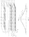
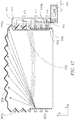
- FIGURE 2 is a schematic diagram illustrating a graph of the variation of display luminance 150 with y-axis viewing angle 152 for the non-imaging backlight of FIGURE 1 .
- light from LEDs 142, 144, 146 is directed through the light guide plate 100 and respective layers of the non-imaging backlight, in a non-Lambertian distribution as illustrated by luminance distribution 154.
- luminance distribution 154 If the operating current of LED 142 is reduced or switched off, then new distribution 156 is created, with the luminance distribution reduced in maximum intensity, however the shape of the distribution has substantially the same angular distribution shape.
- the backlight is a non-imaging type and has substantially a fixed shape angular distribution irrespective of LED drive currents across the array 140.
- FIGURE 3 is a schematic diagram illustrating an electrical arrangement of an LED array for the non-imaging backlight of FIGURE 1 comprising multiple LED strings.
- the LED array 140 is comprised of multiple LED strings 162 comprising multiple LEDs 166 and connected to input 170 by means of electrodes 164, 168.
- the number of connections at input 170 may be substantially lower than the number of LEDs in the array 140.
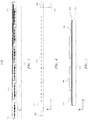
- FIGURE 4 is a schematic diagram illustrating the connections to an LED array for the non-imaging backlight of FIGURE 1 .
- LED assembly 172 may have a small size connection 180 provided by cable 182.
- the height 174 of the assembly may be small due to the small number of connections in the input 170 to the multiple strings 162 of the array 140.
- Advantageously such an arrangement may be achieved in a compact structure suitable for mobile display devices.
- FIGURE 5 is a schematic diagram illustrating a side view of the structure of a pair LEDs of an LED array for the non-imaging backlight of FIGURE 1 .
- Assembly 172 may comprise a substrate 200 and may further comprise an insulator layer 202. Electrodes 164, 168 may be formed on the insulator 202 and used to provide connection to a string of LEDs 166.
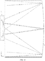
- FIGURE 6 is a schematic diagram illustrating in perspective view, the structure of a display device comprising an imaging directional backlight arranged with a spatial light modulator.
- the operation of waveguide 1 comprising an optical valve will be described below with reference to FIGURES 8 and 9 .
- Light source array 15 may comprise LEDs 15a-n arranged at input side 2 of waveguide 1.
- Rear reflector 81 with reflective structure 83 is arranged to receive light transmitted through features 12 of the waveguide 1.
- Planar features 10 are arranged between features 12 of the waveguide 1.
- Optical stack 254 may comprise diffuser, retarder and reflective polarizer elements.
- FIGURE 7 is a schematic diagram illustrating a graph of the variation of display luminance with viewing angle for the directional backlight of FIGURE 6 for different light source currents.
- light from each LED 15a-n of array 15 is directed with a different angular distribution in the y-axis.
- Control of LEDs can achieve a lateral angular shift from distribution 260 to distribution 262.
- the output angular distributions can be controlled to achieve at least power reduction, privacy operation, high luminance outdoors operation, and/or autostereoscopic operation.
- Optical valves as described in commonly-owned U.S. Patent Application No. 13/300,293 advantageously can be arranged in combination with fast switching transmissive spatial light modulators to achieve time multiplexed autostereoscopic illumination in a thin package while providing high resolution images with flicker free observer tracking and low levels of cross talk.
- Described is a one dimensional array of viewing positions, or windows, that can display different images in a first, typically horizontal, direction, but contain the same images when moving in a second, typically vertical, direction.
- imaging directional backlights are arranged to direct the illumination from multiple light sources through a display panel to respective multiple viewing windows in at least one axis.
- Each viewing window is substantially formed as an image in at least one axis of a light source by the imaging system of the imaging directional backlight.
- An imaging system may be formed between multiple light sources and the respective window images. In this manner, the light from each of the multiple light sources is substantially not visible for an observer's eye outside of the respective viewing window.
- an optical valve is an optical structure that may be a type of light guiding structure or device referred to as, for example, a light valve, an optical valve directional backlight, and a valve directional backlight ("v-DBL").
- optical valve is different to a spatial light modulator (even though spatial light modulators may be sometimes generally referred to as a "light valve” in the art).
- One example of an imaging directional backlight is an optical valve that may employ a folded optical system. Light may propagate substantially without loss in one direction through the optical valve, may be incident on an imaging reflector, and may counter-propagate such that the light may be extracted by reflection off tilted light extraction features, and directed to viewing windows as described in Pat. App. Ser. No. 13/300,293 , which is herein incorporated by reference in its entirety.
- an imaging directional backlight examples include a stepped waveguide imaging directional backlight, a folded imaging directional backlight, a wedge type directional backlight, or an optical valve.
- a stepped waveguide imaging directional backlight may be an optical valve.
- a stepped waveguide is a waveguide for an imaging directional backlight including a waveguide for guiding light, further including a first light guiding surface; and a second light guiding surface, opposite the first light guiding surface, further including a plurality of light guiding features interspersed with a plurality of extraction features arranged as steps.
- a folded imaging directional backlight may be at least one of a wedge type directional backlight, or an optical valve.
- light may propagate within an exemplary optical valve in a first direction from an input side to a reflective side and may be transmitted substantially without loss.
- Light may be reflected at the reflective side and propagates in a second direction substantially opposite the first direction.
- the light may be incident on light extraction features, which are operable to redirect the light outside the optical valve.
- the optical valve generally allows light to propagate in the first direction and may allow light to be extracted while propagating in the second direction.
- the optical valve may achieve time sequential directional illumination of large display areas. Additionally, optical elements may be employed that are thinner than the back working distance of the optical elements to direct light from macroscopic illuminators to a window plane. Such displays may use an array of light extraction features arranged to extract light counter propagating in a substantially parallel waveguide.
- Thin imaging directional backlight implementations for use with LCDs have been proposed and demonstrated by 3M, for example U.S. Patent No. 7,528,893 ; by Microsoft, for example U.S. Patent No. 7,970,246 which may be referred to herein as a "wedge type directional backlight;” by RealD, for example U.S. Patent Application No. 13/300,293 which may be referred to herein as an "optical valve” or “optical valve directional backlight,” all of which are herein incorporated by reference in their entirety.
- the present disclosure provides stepped waveguide imaging directional backlights in which light may reflect back and forth between the internal faces of, for example, a stepped waveguide which may include a first side and a first set of features. As the light travels along the length of the stepped waveguide, the light may not substantially change angle of incidence with respect to the first side and first set of surfaces and so may not reach the critical angle of the medium at these internal faces. Light extraction may be advantageously achieved by a second set of surfaces (the step “risers") that are inclined to the first set of surfaces (the step "treads"). Note that the second set of surfaces may not be part of the light guiding operation of the stepped waveguide, but may be arranged to provide light extraction from the structure.
- a wedge type imaging directional backlight may allow light to guide within a wedge profiled waveguide having continuous internal surfaces. The optical valve is thus not a wedge type imaging directional backlight.
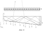
- FIGURES 8-9 are schematic diagrams illustrating in front and side views the propagation of light in a directional waveguide similar to that shown in FIGURE 6 .
- FIGURE 8 is a schematic diagram illustrating a front view of light propagation in one embodiment of a directional display device
- FIGURE 9 is a schematic diagram illustrating a side view of light propagation in the directional display device of FIGURE 8 .
- FIGURE 8 illustrates a front view in the xy plane of a directional backlight of a directional display device, and includes an illuminator array 15 which may be used to illuminate a stepped waveguide 1.
- Illuminator array 15 includes illuminator elements 15a through illuminator element 15n (where n is an integer greater than one).
- the stepped waveguide 1 of FIGURE 8 may be a stepped, display sized waveguide 1.
- Illumination elements 15a through 15n are light sources that may be light emitting diodes (LEDs).
- FIGURE 9 illustrates a side view in the xz plane, and includes illuminator array 15, SLM (spatial light modulator) 48, extraction features 12, guiding features 10, and stepped waveguide 1, arranged as shown.
- SLM spatial light modulator
- the side view provided in FIGURE 9 is an alternative view of the front view shown in FIGURE 8 . Accordingly, the illuminator array 15 of FIGURE 8 and 9 corresponds to one another and the stepped waveguide 1 of FIGURE 8 and 9 may correspond to one another.
- the stepped waveguide 1 may have an input end 2 that is thin and a reflective end 4 that is thick.
- the waveguide 1 extends between the input end 2 that receives input light and the reflective end 4 that reflects the input light back through the waveguide 1.
- the length of the input end 2 in a lateral direction across the waveguide is greater than the height of the input end 2.
- the illuminator elements 15a - 15n are disposed at different input positions in a lateral direction across the input end 2.
- the waveguide 1 has first and second, opposed guide surfaces extending between the input end 2 and the reflective end 4 for guiding light forwards and back along the waveguide 1 by total internal reflection.
- the first guide surface is planar.
- the second guide surface has a plurality of light extraction features 12 facing the reflective end 4 and inclined to reflect at least some of the light guided back through the waveguide 1 from the reflective end in directions that break the total internal reflection at the first guide surface and allow output through the first guide surface, for example, upwards in FIGURE 9 , that is supplied to the SLM 48.
- the light extraction features 12 are reflective facets, although other reflective features could be used.
- the light extraction features 12 do not guide light through the waveguide, whereas the intermediate regions of the second guide surface intermediate the light extraction features 12 guide light without extracting it. Those regions of the second guide surface are planar and may extend parallel to the first guide surface, or at a relatively low inclination.
- the light extraction features 12 extend laterally to those regions so that the second guide surface has a stepped shape including of the light extraction features 12 and intermediate regions.
- the light extraction features 12 are oriented to reflect light from the light sources, after reflection from the reflective end 4, through the first guide surface.
- the light extraction features 12 are arranged to direct input light from different input positions in the lateral direction across the input end in different directions relative to the first guide surface that are dependent on the input position.
- the illumination elements 15a-15n are arranged at different input positions, the light from respective illumination elements 15a-15n is reflected in those different directions.
- each of the illumination elements 15a-15n directs light into a respective optical window in output directions distributed in the lateral direction in dependence on the input positions.
- the lateral direction across the input end 2 in which the input positions are distributed corresponds with regard to the output light to a lateral direction to the normal to the first guide surface.
- the illuminator elements 15a - 15n may be selectively operated to direct light into a selectable optical window.
- the optical windows may be used individually or in groups as viewing windows.
- the reflective end 4 may have positive optical power in the lateral direction across the waveguide.
- the optical axis may be defined with reference to the shape of the reflective end 4, for example being a line that passes through the center of curvature of the reflective end 4 and coincides with the axis of reflective symmetry of the end 4 about the x-axis.
- the optical axis may be similarly defined with respect to other components having optical power, for example the light extraction features 12 if they are curved, or the Fresnel lens 62 described below.
- the optical axis 238 is typically coincident with the mechanical axis of the waveguide 1.
- the SLM 48 extends across the waveguide is transmissive and modulates the light passing therethrough.
- the SLM 48 may be a liquid crystal display (LCD) but this is merely by way of example, and other spatial light modulators or displays may be used including LCOS, DLP devices, and so forth, as this illuminator may work in reflection.
- the SLM 48 is disposed across the first guide surface of the waveguide and modulates the light output through the first guide surface after reflection from the light extraction features 12.
- FIGURE 8 The operation of a directional display device that may provide a one dimensional array of viewing windows is illustrated in front view in FIGURE 8 , with its side profile shown in FIGURE 9 .
- the light may propagate along +x in a first direction, within the stepped waveguide 1, while at the same time, the light may fan out in the xy plane and upon reaching the far curved end side 4, may substantially or entirely fill the curved end side 4.
- the light While propagating, the light may spread out to a set of angles in the xz plane up to, but not exceeding the critical angle of the guide material.
- the extraction features 12 that link the guiding features 10 of the bottom side of the stepped waveguide 1 may have a tilt angle greater than the critical angle and hence may be missed by substantially all light propagating along +x in the first direction, ensuring the substantially lossless forward propagation.
- the curved end side 4 of the stepped waveguide 1 may be made reflective, typically by being coated with a reflective material such as, for example, silver, although other reflective techniques may be employed.
- Light may therefore be redirected in a second direction, back down the guide in the direction of - x and may be substantially collimated in the xy or display plane.
- the angular spread may be substantially preserved in the xz plane about the principal propagation direction, which may allow light to hit the riser edges and reflect out of the guide.
- light may be effectively directed approximately normal to the xy display plane with the xz angular spread substantially maintained relative to the propagation direction. This angular spread may be increased when light exits the stepped waveguide 1 through refraction, but may be decreased somewhat dependent on the reflective properties of the extraction features 12.
- reflection may be reduced when total internal reflection (TIR) fails, squeezing the xz angular profile and shifting off normal.
- TIR total internal reflection
- the increased angular spread and central normal direction may be preserved.
- light may exit the stepped waveguide 1 approximately collimated and may be directed off normal in proportion to the y-position of the respective illuminator element 15a - 15n in illuminator array 15 from the input edge center. Having independent illuminator elements 15a - 15n along the input edge 2 then enables light to exit from the entire first light directing side 6 and propagate at different external angles, as illustrated in FIGURE 8 .
- FIGURE 10 is a schematic diagram illustrating a privacy directional display device which includes an imaging directional backlight.
- 2D display systems may also utilize directional backlighting for security and efficiency purposes in which light may be primarily directed at the eyes of a first viewer 45 as shown in FIGURE 10 .
- first viewer 45 may be able to view an image on device 50
- light is not directed towards second viewer 47.
- second viewer 47 is prevented from viewing an image on device 50.
- Each of the embodiments of the present disclosure may advantageously provide autostereoscopic, dual image or privacy display functions.
- Angular illumination control is advantageously achieved through independent control of LEDs 15a-n of the array 15.
- FIGURE 11 is a schematic diagram illustrating a directional display apparatus comprising a display device and a control system.
- the display device may comprise a directional backlight comprising waveguide 1, parallax element 100 and spatial light modulator 48 arranged in series.
- Further touch screen 102 may be arranged in series with the spatial light modulator 48, with the spatial light modulator typically arranged between the touch screen 102 and waveguide.
- Viewing windows 26 may be provided at window plane 106.
- Further viewing windows 27 may be produced by light from the waveguide 1 at window plane 107. Viewing windows 27, 26 may be substantially aligned with one another and window planes 106, 107 may be substantially coplanar and superimposed.
- Spatial light modulator 48 may cooperate with parallax element 100 to produce further viewing windows 29 at window plane 109. As will be described below, the viewing windows 29, 26 may be aligned and may have common window plane 106, 109 locations.
- control system The arrangement and operation of the control system will now be described and may be applied, with changes as necessary, to each of the display devices disclosed herein.
- the directional display device comprises a directional backlight that comprises waveguide 1 and an array of illuminator elements 15 arranged as described above.
- the control system is arranged to selectively operate the illumination elements 15a-15n of the array of illuminator elements 15, to direct light into selectable optical windows, in combination the optical windows providing viewing windows 26.
- the control system may comprise a sensor system arranged to detect the position of the observer 99 relative to the display device 100.
- the sensor system may include a position sensor 70, such as a camera with image capture cone 71 directed towards viewing window 26, and a head position measurement system 72 that may for example comprise a computer vision image processing system.
- the control system may further comprise an illumination controller 74 and an image controller 76 that are both supplied with the detected position of the observer supplied from the head position measurement system 72.
- the illumination controller 74 selectively operates the illuminator elements 15a-15n to direct light to into the viewing windows 26 in cooperation with waveguide 1.
- the illumination controller 74 selects the illuminator elements 15a-15n to be operated in dependence on the position of the observer detected by the head position measurement system 72, so that the viewing windows 26 into which light is directed are in positions corresponding to the left and right eyes of the observer 99. In this manner, the lateral output directionality of the waveguide 1 corresponds with the observer position.
- the image controller 76 controls the SLM 48 to display images.
- Image controller 76 may be connected to pixel drive element 105 on the spatial light modulator 48 arranged to address the pixels of the spatial light modulator as will be further described below.
- the image controller 76 and the illumination controller 74 may operate as follows.
- the image controller 76 controls the SLM 48 to display temporally multiplexed left and right eye images.
- the illumination controller 74 operate the light sources 15a-15n to direct light into viewing windows in positions corresponding to the left and right eyes of an observer synchronously with the display of left and right eye images. In this manner, an autostereoscopic effect is achieved using a time division multiplexing technique.
- a directional display apparatus may further include a control system which may be arranged to selectively operate the light sources to direct light into viewing windows corresponding to output directions as previously discussed.
- This embodiment may also be used in conjunction with any of the directional backlights, directional display devices, directional display apparatuses, and so forth as described herein.
- a directional display apparatus may be an autostereoscopic display apparatus with a control system.
- the control system may be further arranged to control the directional display device to temporally display multiplexed left and right images and to substantially synchronously direct the displayed images into viewing windows in positions corresponding to at least the left and right eyes of an observer.
- the control system may include a sensor system which may be arranged to detect the position of an observer across the display device, and the control system also may be arranged to direct the displayed images into viewing windows in positions corresponding to at least the left and right eyes of an observer. The position of the viewing windows may primarily depend on the detected position of the observer.
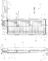
- FIGURE 12 is a schematic diagram illustrating in front view a light source array connection assembly 300 for a directional backlight.
- each light source 15a-n of array 15 may be individually addressable.
- Each light source 15a-n may for example be a single LED or may further comprise multiple light sources such as multi-chip LED packages or strings of packages.
- the strings of packages may be wired in series to reduce the overall number of electrode tracks 304 however this may reduce the addressability of directional control of light when the light bar is used with a directional light guide plate.
- the number of individually addressable light sources 12a-n may be for example at least 8 and more typically between 12 and 48 in a mobile display of diagonal 4". Larger displays may have larger number of individually addressable light sources. For example a 14" display may typically comprise 60 LEDs, or which 12 or more may be in individually addressable strings.
- Light source controller 74 supplies current load to the individually addressable light sources 15a-n through cable 303 and connector 302. Electrode tracks 304, 308 are used as input and output electrodes to each of the light sources 15a-n.
- the fan-out area of the electrode tracks 304 requires height 310 of the connection assembly 300 that disadvantageously increases the display physical volume, undesirably increasing footprint and/or thickness in comparison to the connector size for non-imaging backlights.
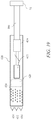
- FIGURE 13A is a schematic diagram illustrating in side views a light source array connection assembly 300 for an imaging directional backlight.
- Light source 15a may comprise a package 353 comprising electrical connection and heat slug parts; light emitting region 351 that produces a distribution 357 of light with axis 471.
- the axis 471 may be outwards from the face of the insulator 314, whereas in a side emitting LED, the axis 471 may be parallel to the face of the insulator 314 as will be described herein.
- Assembly 300 may comprise a metal core (or clad) printed circuit board (MCPCB) comprising a metal heat sink layer 312, an insulator layer 314 and electrode layer comprising electrode tracks 304, 308.
- Connector 302 may have a physical height 316 for example 1mm while MCPCB comprising layers 312, 314 may have height 317 which may be 0.2mm.
- the combination of heights 317, 316 disadvantageously increases the display physical volume, undesirably increasing footprint and/or thickness in comparison to the connector size for non-imaging backlights.
- the package 353 may comprise more than one addressable light source; thus one package may comprise multiple light emitting regions 351.
- Advantageously fewer package mounting operations may be required during the alignment of the packages to the array on the MCPCB 312, 314, reducing cost.
- FIGURE 13B is a schematic diagram illustrating in side view a dual layer metal core printed circuit board that can be used for providing parallel connectivity in limited areas.
- Conductive layers 315 and 317 may be formed with intermediate additional insulator layer 319.
- Electrode tracks 304, 308 may be formed by means of forming via holes to layer 315 as well as in layer 317. However such elements are expensive and complicated to remove.
- the connector size for imaging directional backlights should be reduced, preferably with low cost MCPCB construction.
- FIGURES 14-15 are schematic diagrams illustrating in front view light source array connection assemblies for a directional backlight.
- multiple connectors 322, 324, 326 may be introduced, thus reducing height 320 in comparison to height 310 in FIGURE 12 .
- Connector height 316 remains in the region near to the LEDs, that can increase display thickness or footprint area. Typically there is some allowable space outside the panel footprint in the system design.
- FIGURE 15 shows that the tracks 304 can have a 90 degree bend, providing a side location for connector 302, however the height 330 of connection assembly 300, which is typically an MCPCB, is substantially increased and cost increased.
- connection assembly for an array 15 of individually addressable light sources 15 a-n, with low footprint area and thickness, suitable for dense connectivity in a mobile display platform with small volume and reduced cost.
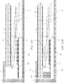
- FIGURES 16-17 are schematic diagrams illustrating in side and front views of flat connectors for a light source array parallel connection assembly for a directional backlight.
- Plural flat connectors 400, 402, 404 each comprise an array of separate conductive tracks 409. In operation, the flat connectors 400, 402, 404 are mounted in a stack 415. Each connector may further comprise connection regions 406, that may comprise holes with connection to conductive tracks 409. Flat connectors 400, 402, 404 may have thickness of 100microns for example. The length of each flat connector may be different.
- the flat connectors 400, 402, 404 may be Flat Flexible Cable (FFC's) that are made up of thin rectangular copper conductors laminated between two layers of polyester insulation for example. Alternatively the flat connectors may be Flexible Printed Circuits (FPC's) that are similar in construction to FFC's except that copper film is chemically etched to produce the desired electrode pattern.
- FFC's Flexible Printed Circuits
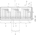
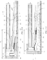
- FIGURES 18A-18B are schematic diagrams illustrating in front and side views a light source array mounting strip 410 for a directional backlight.
- the mounting strip 410 includes an electrical insulator layer 314 extending in a lateral direction (y direction) and shaped into: an end portion 401 having a face; and a base 403 portion extending from the face of the end portion 401.
- Line 405 may be provided about which the end and base portions 403, 401 are shaped.
- the mounting strip may be provided with multiple regions 414, 416, 418 of light sources 15a-n of the array 15 that are connected by means of electrical tracks 304, 308 to respective connection regions 421, 417, 419 comprising connector features 412.
- the mounting strip 410 thus further comprises a heat sink layer 312 extending at least across said end portion 401 on the opposite side of the electrical insulator layer 314 from the conductive tracks 304 and the heat sink layer 312 may comprise a layer of metal that may be copper or aluminium for example.
- the heat sink layer 312 may further extend across the end portion 401 and the base portion 403.
- FIGURE 18C is a schematic diagram illustrating in front view a light source array mounting strip 410 for a directional backlight.
- regions 401 and optionally region 403 may be colored with a colored overcoat for example a solder mask layer that is for example black or white. Black solder mask can reduce the back reflections from the bar and improve the leakage of light from the intended direction.
- a white overcoat or solder mask layer can advantageously improve the overall brightness of the display.
- the color overcoat may optionally be applied in a region 500 which may not align with the electrical grouping of the electrodes (as illustrated) and is chosen for optical performance reasons.
- the region 500 may be one color for example white and the region of the bar outside region 500 may be a different color for example black.
- the brightness of the display may be improved in the central position and the leakage of light from the intended directions may be reduced.
- FIGURE 19 is a schematic diagram illustrating in front view an interface connector assembly 420 for a directional backlight light source array.
- Assembly 420 may comprise a PCB with connector features 428 in blocks 430, 432, 434.
- Connector 303 connected to control system 74 by means of connector 424 may be arranged to address LED current control element 422.
- Element 422 may be used to provide individually controllable constant current values for the output of each light source 15a-n in response to control signals from control system 74.
- element 422 may comprise one or more chips such as the iW7032 manufactured by Dialog Semiconductor. Fan out track region 426 may be provided to connect features 428 to element 422.
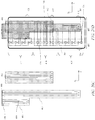
- FIGURES 20A-20B are schematic diagrams illustrating in side and front views a light source array parallel connection assembly for a directional backlight.
- the arrangement comprises a mounting strip 410 including an electrical insulator layer 314 extending in a lateral direction, such as the y direction, which may be shaped into an end portion 401 having a face; and a base portion 403 extending from the face of the end portion.
- An array of light sources 15a-n is mounted to the face of the end portion 401 of the mounting strip 410 arrayed in said lateral direction, and arranged to output light outwardly from said face.
- Separate conductive tracks 304 are connected to each respective light source 15a-n formed on the electrical insulator layer 314 of the mounting strip 410 and extending across the end portion 401 and onto the base portion 403.
- the plural flat connectors 400, 402, 404 each comprising an array of separate conductive tracks 409, are mounted in a stack 415 on the base portion of the mounting strip 410, each conductive track 304 on the mounting strip 410 being electrically connected to a respective conductive track 409 of one of the flat connectors 400, 402, 404, the flat connectors 400, 402, 404 extending in said lateral direction along the base portion to at least one region 429 outside the base portion 403, allowing electrical connection to be made to the conductive tracks 409 of the flat connectors 400, 402, 404 outside the base portion.
- the array of light sources 15a-n may also be provided with one or more common electrodes 308.
- the flat connector 404 may be mounted on the base portion 403 followed by the flat connector 402 and finally the flat connector 400.
- the number of flat connectors may be two or more.
- Each conductive track 304, 308 on the mounting strip is directly electrically connected to a respective conductive track 409 of one of the flat connectors 400, 402, 404.
- Connector blocks 430, 432, 434 are connected to each flat connector 400, 402, 404 outside the base portion 403, which connector blocks 430, 432, 434 allow electrical connection to be made to the conductive tracks 409 of the flat connectors 400, 402, 404.
- the conductive tracks 409 of each flat connector 400, 402, 404 are exposed outside the base portion 403 to allow electrical connection to be made to them.
- a light source array parallel connection assembly for a directional backlight may comprise a mounting strip 410 including an electrical insulator layer 314 extending in a lateral direction, the mounting strip 410 including an end portion 401 and a base portion 403.
- An array of light sources 15a-n may be mounted to the end portion 401 of the mounting strip 410 arrayed in said lateral direction, and arranged to output light in a forward direction.
- Separate conductive tracks 304 may be connected to each respective light source 15a-n formed on the electrical insulator layer 314 of the mounting strip 410 and extending from the end portion 401 onto the base portion 403.
- each flat connector 400, 402, 404 comprising an array of separate conductive tracks 409, the flat connectors 400, 402, 404 being mounted in a stack 415 on the base portion 403 of the mounting strip 410, each conductive track 304 on the mounting strip being electrically connected to a respective conductive track 309 of one of the flat connectors 400, 402, 404.
- the flat connectors 400, 402, 404 may extending in said lateral direction along the base portion 403 to outside the base portion, allowing electrical connection to be made to the conductive tracks 409 of the flat connectors 400, 402, 404 outside the base portion.
- Each conductive track on the mounting strip 410 may be directly electrically connected to a respective conductive track 409 of one of the flat connectors.
- the mounting strip 410 may further comprise a heat sink layer 312 extending at least across said end portion 403 on the opposite side of the electrical insulator layer 314 from the conductive tracks 304.
- the heat sink layer 312 may extend across the end portion 401 and the base portion 403 and may comprise a layer of metal that may be copper or aluminum.
- the width of the mounting strip can be minimized. Further, as the number of light sources is increased, the width of mounting strip can be maintained by increasing the number of flat connectors.
- the interface connector assembly 420 may be arranged along the short edge of the SLM 48 while the light sources are arranged along the long edge.
- Advantageously high efficiency illumination can be achieved in a compact package.
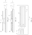
- FIGURES 20C-20D are schematic diagrams illustrating in front views light source array parallel connection assembly for a directional backlight comprising partially overlapping flat connectors.
- FIGURE 20C illustrates a pair of flat connectors 400, 402 and FIGURE 20D illustrates the arrangement of flat connectors 400, 402 when connected to the mounting strip 410.
- Mounting strip 400 may have two regions 481, 483 with first and second lengths arranged to connect to connection regions 421, 419.
- Mounting strip may be arranged to connect to region 417.
- the total thickness of the stack 415 of flat connectors 400, 402 may be reduced.
- the outer light sources of the array 15a-n connected to regions 419, 421 may be provided for example as strings of multiple LEDs.
- the inner light sources connected to region 417 may be provided as either individually addressable LEDs or strings with fewer LEDs than those connected to the outer regions.
- the outer light sources may be required to have lower current drive characteristics compared to the inner light sources.
- more LEDs may be connected in series, reducing the number of connections.
- the number of flat connectors may be reduced, reducing total device thickness.
- FIGURES 21A-21C are schematic diagrams illustrating in side views a directional display comprising a light source array connection system comprising top and side emitting LEDs respectively.
- the thickness of the input side 2 of the waveguide 1 is thinner than the end 4 comprising a mirror.
- the additional space available can be used for placement of the base portion 403 of the mounting strip 410.
- FIGURES 21A-C show arrangements wherein the base portion 403 extends in the forward direction from the light sources 15a-n.
- the light sources 15a-n are mounted to the mounting strip 410 on a face of the end portion 401 in a top-emitting configuration so that the forward direction is outwardly of the face.
- the mounting strip 410 is shaped so the base portion 403 extends in the forward direction.
- light source of the array 15a-n comprises a top emitting LED, that is light rays are emitted in a cone with an axis 471 directed outwardly from the face of the end portion 401.
- the strip 410 is shaped so that in the region of the line 405, the electrical insulator 314 is shaped by a bend that may be linear into the end portion 401 and the base portion 403.
- the base portion 403 extends forwards of the face of the end portion 401.
- the base portion 403 and flat connector stack 415 is thus arranged under the rear reflector 81 and waveguide 1.
- a further rear bezel 473 that provides mechanical stability for the display apparatus may be arranged between the flat connector stack 415 and optical elements 1, 81, 48.
- the strip 405 may be connected to the frame 472 of the display device by means of a thermally conductive layer 470 to provide for mechanical stability and heat sinking of the light sources through to the frame during operation.
- a thermally conductive layer 470 to provide for mechanical stability and heat sinking of the light sources through to the frame during operation.
- the junction temperature of the LED may be reduced, increasing efficiency.
- a thin stack can be achieved with multiple individually addressable light sources 15a-n.
- directional backlight comprising a waveguide 1 comprising an input end 2 for receiving input light and first and second, opposed guide surfaces 6,8 for guiding input light along the waveguide 1, wherein the second guide surface 8 is arranged to deflect light guided through the waveguide 1 out of the waveguide 1 through the first guide surface 6 as output light, and the waveguide 1 is arranged to direct the output light into optical windows 26 in output directions that are distributed laterally in dependence on the input position of the input light laterally along the input end 2; and a connection assembly as described herein arranged with the light sources 15a-n disposed at different input positions laterally along the input end 2 of the waveguide 1, facing the input end 2 of the waveguide 1 for supplying said input light.
- a directional display device may comprise said directional backlight and a transmissive spatial light modulator 48 comprising an array of pixels 130, 132, 134 arranged to receive the output light from the waveguide 1 and to modulate it to display an image.
- a directional display apparatus may comprise said directional display device and a control system 74 connected to the flat connectors 400, 402, 404 outside the base portion 403 for providing connection to the light sources 15a-n, the control system being arranged to control the light sources 15a-n to direct light into optical windows 26 for viewing by an observer 99.
- a directional display can achieve addressable directionality in a compact package.
- bezel width that is the distance 475 between the edge of the pixels 130, 132, 134 of the active area and the outer edge of the frame 472 for the device.
- FIGURE 21B shows an arrangement wherein the base portion 403 extends outwardly of the end portion 401.
- the base portion 403 extends in the forward direction.
- Light source 15a comprises a side emitting LED, that is light rays are emitted in a cone with axis 471 parallel to the face of the end portion 401 into the end 2 of the waveguide 1.
- the strip 410 is shaped so that the base portion 403 is rearwards with respect to the face portion 401.
- the light sources 15a-n are thus mounted to the mounting strip 410 on a face of the end portion 401 in a side-emitting configuration so that the forward direction is across the face.
- the heat sink layer 312 is not positioned between the light source and the outer frame, reducing bezel width 477.
- the apparatus may further comprise a further heat sink element thermally connected to the heat sink layer 312 adjacent the end portion 403.
- heat sink layer 312 of the strip 410 may be further thermally connected to the rear bezel 473, advantageously improving heat sink performance and reducing LED junction temperature, increasing efficiency.
- FIGURE 21C shows a further embodiment wherein the end portion and base portion are co-planar.
- the light sources 15a-n are mounted to the mounting strip 410 on a face of the end portion 401 in a side-emitting configuration so that the forward direction is across the face.
- the base portion 403 extends in the forward direction.
- the heat sink layer 312 is not distorted and an increased thickness and stiffer material can be used. Further, the heat sink layer 312 may be bonded to the frame 472, increasing thermal heat sinking capability.
- FIGURE 21D shows a further embodiment wherein an additional electrically and thermally conductive element 485 is arranged between the light source 15a and MCPCB 312 ; advantageously the light source 15a may be provided by a top emitting LED of simpler construction than the side emitting LED of FIGURE 21C .
- light source 15a may have an emitting region 351 that is offset from the center of the package 353. Further polarizer 118 may be trimmed to enable the light source to extend above the emitting region, conveniently achieving a larger surround for the light source.
- a compact arrangement of light sources with respect to the spatial light modulator may be achieved.
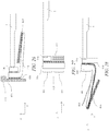
- FIGURES 22-23 are schematic diagrams illustrating in side view a method to solder connection cables to a light source array assembly for a directional backlight.
- the flat connector 400 comprising holes 406 and electrode tracks 409 are aligned with features 412 that comprise solder regions on electrode tracks 304, 308.
- a solder plug or "rivet" as shown in FIGURE 23 is formed that advantageously provides both mechanical and electrical connection in a low profile between the MCPCB of the strip 410 and flat connector 400.
- FIGURE 24 is a schematic diagram illustrating in front view a method to solder connection cables to a light source array assembly for a directional backlight.
- the tracks 304, 409 may respectively have bond regions 412, 407 that are elongate and holes 406 are offset between adjacent tracks 409. In this manner, the strength of the bond seam can advantageously be increased.
- connection to the interface connector assembly should be removable.
- FIGURES 25A-25B are schematic diagrams illustrating in side and front views a light source array connection system for a directional backlight.
- FIGURE 20B illustrates the use of solder plug method of FIGURES 22-23 .
- FIGURES 25A-B show flat connectors 400, 402, 404 with connectors 440 so that removable connection can be provided for attachment to interface connector assembly 420 by means of mating connectors 442.
- FIGURES 26-31 are schematic diagrams illustrating in side view the arrangement of a light source array assembly and a directional light guide plate in a display assembly.
- the light sources 15a-n are mounted to the mounting strip 410 on a face of the end portion 401 in a top-emitting configuration so that the forward direction is outwardly of the face.
- FIGURE 26 shows an arrangement wherein the base portion 403 extends in the forward direction from the light sources 15a-n. Further the mounting strip 410 is shaped so the base portion 403 extends in the forward direction.
- FIGURE 26 illustrates a side frame 472 with recess 474, arranged to advantageously reduce bezel width 475 in comparison to the arrangement of FIGURE 21A .
- FIGURE 27 illustrates a strip 410 comprising coplanar end portion 401 and base portion 403 with a vertical orientation with respect to the waveguide 1.
- the thickness of the heat sink layer 312 may be increased.
- FIGURES 28-29 illustrate strip 410 with various degrees of reverse bends so that the base portion 403 is extended rearwards with respect to the end portion 401.
- the mounting strip 410 is shaped so that the base portion 403 is disposed on the rearward side of the end portion 401.
- the flat connectors are stacked away from the waveguide 1, reducing complexity of assembly for systems with sufficient assembly space outside the active area of the spatial light modulator 48.
- the mounting strip 410 is shaped so that the base portion is disposed on the rearward side of the end portion extending parallel to the end portion 401.
- the extent of the rearward facing base region 403 is reduced.
- FIGURES 30-31 illustrate arrangements where the spatial light modulator overlays the array 15 of light sources with co-planar and rearwards base regions 403.
- the light sources 15a-n are mounted to the mounting strip 410 on a face of the end portion 401 in a side-emitting configuration so that the forward direction is across the face.
- FIGURE 30 the base portion 403 extends in the rearward direction whereas FIGURE 31 shows an arrangement wherein the base portion 403 extends in the forward direction from the light sources 15a-n.
- FIGURE 32 illustrates an example arrangement where arrays of light sources 519a-n may be positioned on a base portion 410.
- the base portion may be bent out of plane for example along the dotted line 610.
- FIGURE 32 illustrates 6 light sources on each side, however light sources may be on one side only or may comprise different numbers of light sources for example as illustrated in FIGURE 20 .
- the connection regions 421, 417, 419 may be positioned to provide connections for flat cables that connect in a stack to connectors 442, similar to those described with reference to FIGURE 20 .
- the overlapped connector cables reduce the space occupied by connectors.
- Connectors 442 may be addressed by LED current control element 422 and further connector 424 on assembly 420.
- the light sources 519a-n may be mounted at an angle to match the structure 523 of light guide plate 504.
- the light sources 519a-n may also be mounted at an independent angle to the structure 592, 594 of the light guide plate 504.
- the arrangement may also comprise a further array of light sources 502a-n on base portion similar to 410 (not shown) arranged to input light in to the light guide plate 504 from another side.
- the embodiments described can be adapted to minimize the fan-out width for different designs of directional light guide plates including those designed for one or more side illumination light sources.
- Advantageously individually addressable light sources may be provided in a very compact arrangement suitable for thin displays, for example mobile displays that achieve power savings, outdoors operation, switchable privacy operation and autostereoscopic operation.
- the terms “substantially” and “approximately” provide an industry-accepted tolerance for its corresponding term and/or relativity between items. Such an industry-accepted tolerance ranges from zero percent to ten percent and corresponds to, but is not limited to, component values, angles, et cetera. Such relativity between items ranges between approximately zero percent to ten percent.
- Embodiments of the present disclosure may be used in a variety of optical systems.
- the embodiment may include or work with a variety of projectors, projection systems, optical components, displays, microdisplays, computer systems, processors, self-contained projector systems, visual and/or audiovisual systems and electrical and/or optical devices.
- aspects of the present disclosure may be used with practically any apparatus related to optical and electrical devices, optical systems, presentation systems or any apparatus that may contain any type of optical system. Accordingly, embodiments of the present disclosure may be employed in optical systems, devices used in visual and/or optical presentations, visual peripherals and so on and in a number of computing environments.
Landscapes
- Physics & Mathematics (AREA)
- General Physics & Mathematics (AREA)
- Optics & Photonics (AREA)
- Nonlinear Science (AREA)
- Chemical & Material Sciences (AREA)
- Crystallography & Structural Chemistry (AREA)
- Microelectronics & Electronic Packaging (AREA)
- Engineering & Computer Science (AREA)
- Mathematical Physics (AREA)
- Condensed Matter Physics & Semiconductors (AREA)
- Computer Hardware Design (AREA)
- Power Engineering (AREA)
- Planar Illumination Modules (AREA)
Claims (15)
- Parallele Lichtquellenarray-Verbindungsanordnung für eine gerichtete Hintergrundbeleuchtung, wobei die Anordnung Folgendes umfasst:ein Montageband (410), das eine elektrische Isolierschicht (314) enthält, die sich beide in eine seitliche Richtung erstrecken, wobei das Montageband (410) einen Endabschnitt (401) und einen Basisabschnitt (403) enthält, die senkrecht zu der seitlichen Richtung angeordnet sind;ein Array von Lichtquellen (15), das an dem Endabschnitt (401) des Montagebands (410) montiert ist, das in der seitlichen Richtung angeordnet ist, und das angeordnet ist, um Licht in eine Vorwärtsrichtung auszugeben;separate Leiterbahnen (304), die mit jeder entsprechenden Lichtquelle (15) verbunden sind, die an der elektrischen Isolierschicht (314) des Montagebands (410) gebildet sind und sich von dem Endabschnitt (401) auf den Basisabschnitt (403) erstrecken; undgekennzeichnet durchmehrere Flachstecker (400, 402, 404), wobei jeder ein Array von separaten Leiterbahnen (409) umfasst, die Flachstecker (400, 402, 404) in einem Stapel an dem Basisabschnitt (403) des Montagebands (410) montiert sind, jede Leiterbahn (304) an dem Montageband (410) elektrisch mit einer entsprechenden Leiterbahn (409) von einem der Flachstecker (400, 402, 404) verbunden ist, sich die Flachstecker (400, 402, 404) in die seitliche Richtung entlang des Basisabschnitts (403) zu außerhalb des Basisabschnitts (403) erstrecken, wobei eine elektrische Verbindung mit den Leiterbahnen (409) der Flachstecker (400, 402, 404) außerhalb des Basisabschnitts (403) ermöglicht wird.
- Anordnung nach Anspruch 1, wobei jede Leiterbahn (304) an dem Montageband (410) direkt elektrisch mit einer entsprechenden Leiterbahn (409) von einem der Flachstecker (400, 402, 404) verbunden ist.
- Anordnung nach Anspruch 1 oder 2, wobei das Montageband (410) ferner eine Wärmeableitschicht (312) umfasst, die sich mindestens über den Endabschnitt (401) an der gegenüberliegenden Seite der elektrischen Isolierschicht (314) von den Leiterbahnen (304) erstreckt, wobei sich optional die Wärmeableitschicht (312) über den Endabschnitt (401) und den Basisabschnitt (403) erstreckt.
- Anordnung nach Anspruch 3, wobei die Wärmeableitschicht (312) eine Schicht aus Metall, optional Kupfer, umfasst.
- Anordnung nach Anspruch 3 oder 4, umfassend ein weiteres Wärmeableitelement, das thermisch mit der Wärmeableitschicht (312) angrenzend an den Endabschnitt (401) verbunden ist.
- Anordnung nach einem der vorhergehenden Ansprüche, ferner umfassend entsprechende Verbindungsblöcke (430, 432, 434), die mit jedem Flachstecker (400, 402, 404) außerhalb des Basisabschnitts (403) verbunden sind, wobei die Verbindungsblöcke (430, 432, 434) eine Herstellung einer elektrischen Verbindung mit den Leiterbahnen (409) des Flachsteckers (400, 402, 404) ermöglichen.
- Anordnung nach einem der Ansprüche 1 bis 5, wobei die Leiterbahnen (409) von jedem Flachstecker (400, 402, 404) außerhalb des Basisabschnitts (403) freigelegt sind, um die Herstellung einer elektrischen Verbindung damit zu ermöglichen.
- Anordnung nach einem der vorhergehenden Ansprüche, wobei der Endabschnitt (401) planar ist und der Basisabschnitt (403) planar ist.
- Anordnung nach einem der vorhergehenden Ansprüche, wobei sich der Basisabschnitt (403) in die Vorwärtsrichtung von den Lichtquellen (15) erstreckt.
- Anordnung nach einem der Ansprüche 1 bis 8, wobei die Lichtquellen (15) an dem Montageband (410) an einer Fläche des Endabschnitts (401) in einer nach oben emittierenden Konfiguration montiert sind, sodass die Vorwärtsrichtung auswärts der Fläche ist, wobei optional das Montageband (410) geformt ist, sodass sich der Basisabschnitt (403) in die Vorwärtsrichtung erstreckt und/oder an der hinteren Seite des Endabschnitts (401) angeordnet ist.
- Anordnung nach Anspruch 10, wobei das Montageband (410) geformt ist, sodass der Basisabschnitt (403) an der hinteren Seite des Endabschnitts (401) angeordnet ist, der sich parallel zu dem Endabschnitt (401) erstreckt.
- Anordnung nach einem der Ansprüche 1 bis 8, wobei die Lichtquellen (15) an dem Montageband (410) an einer Fläche des Endabschnitts (401) in einer seitlich emittierenden Konfiguration montiert sind, sodass die Vorwärtsrichtung über der Fläche ist, wobei sich der Basisabschnitt (403) in die Vorwärtsrichtung oder in die Rückwärtsrichtung erstreckt.
- Gerichtete Hintergrundbeleuchtung, umfassend:einen Wellenleiter (1), umfassend ein Eingangsende (2) zum Empfangen von Eingangslicht und eine erste und eine zweite gegenüberliegende Leitfläche zum Leiten von Eingangslicht entlang des Wellenleiters (1), wobei die zweite Leitfläche angeordnet ist, um Licht, das durch den Wellenleiter (1) geleitet wird, aus dem Wellenleiter durch die erste Leitfläche als Ausgangslicht zu beugen, und der Wellenleiter (1) angeordnet ist, um das Ausgangslicht in optische Fenster in Ausgangsrichtungen zu leiten, die seitlich in Abhängigkeit von der Eingangsposition des Eingangslichts entlang des Eingangsendes (2) verteilt sind; undeine Anordnung nach einem der vorhergehenden Ansprüche, die mit den Lichtquellen (15) angeordnet ist, die an verschiedenen Eingangspositionen seitlich entlang des Eingangsendes des Wellenleiters (1) angeordnet sind, die dem Eingangsende des Wellenleiters (1) zum Zuführen des Eingangslichts zugewandt sind.
- Gerichtete Anzeigevorrichtung, umfassend:eine gerichtete Hintergrundbeleuchtung nach Anspruch 13; undeinen durchlässigen räumlichen Lichtmodulator (48), der ein Pixelarray umfasst, das angeordnet ist, um das Ausgangslicht von dem Wellenleiter (1) zu empfangen und um es zu modulieren, um ein Bild anzuzeigen.
- Gerichtete Anzeigevorrichtung, umfassend:eine gerichtete Anzeigevorrichtung nach Anspruch 14; undein Steuersystem (74), das mit den Flachsteckern (400, 402, 404) außerhalb des Basisabschnitts (403) verbunden ist, um eine Verbindung mit den Lichtquellen (15) bereitzustellen, wobei das Steuersystem (74) angeordnet ist, um die Lichtquellen (15) zu steuern, um Licht zur Ansicht von einem Betrachter in optische Fenster zu leiten.
Applications Claiming Priority (2)
| Application Number | Priority Date | Filing Date | Title |
|---|---|---|---|
| US201462061467P | 2014-10-08 | 2014-10-08 | |
| PCT/US2015/054523 WO2016057690A1 (en) | 2014-10-08 | 2015-10-07 | Directional backlight |
Publications (3)
| Publication Number | Publication Date |
|---|---|
| EP3204686A1 EP3204686A1 (de) | 2017-08-16 |
| EP3204686A4 EP3204686A4 (de) | 2018-06-20 |
| EP3204686B1 true EP3204686B1 (de) | 2019-07-17 |
Family
ID=55653730
Family Applications (1)
| Application Number | Title | Priority Date | Filing Date |
|---|---|---|---|
| EP15848224.0A Active EP3204686B1 (de) | 2014-10-08 | 2015-10-07 | Verbindungseinheit für eine direktionale rückbeleuchtung |
Country Status (4)
| Country | Link |
|---|---|
| US (1) | US9835792B2 (de) |
| EP (1) | EP3204686B1 (de) |
| CN (1) | CN107003563B (de) |
| WO (1) | WO2016057690A1 (de) |
Families Citing this family (6)
| Publication number | Priority date | Publication date | Assignee | Title |
|---|---|---|---|---|
| CN103995361B (zh) * | 2014-06-17 | 2017-01-11 | 上海新视觉立体显示科技有限公司 | 裸眼3d显示像素单元及多视图裸眼3d图像显示设备 |
| EP4124795B1 (de) * | 2016-05-23 | 2024-04-10 | RealD Spark, LLC | Direktionale hintergrundleuchten zur weitwinkelbildgebung |
| JP6689180B2 (ja) * | 2016-11-30 | 2020-04-28 | ミネベアミツミ株式会社 | 面状照明装置 |
| JP6826684B2 (ja) * | 2020-04-07 | 2021-02-03 | ミネベアミツミ株式会社 | 面状照明装置 |
| CN111638606B (zh) * | 2020-06-11 | 2021-12-03 | 武汉华星光电技术有限公司 | 显示面板 |
| US20230019747A1 (en) * | 2022-09-23 | 2023-01-19 | Richard Jones | Hybrid laser architecture with asymmetric metal shunt |
Family Cites Families (409)
| Publication number | Priority date | Publication date | Assignee | Title |
|---|---|---|---|---|
| US1128979A (en) | 1912-06-01 | 1915-02-16 | Walter Hess | Stereoscopic picture. |
| US1970311A (en) | 1931-02-14 | 1934-08-14 | Bell Telephone Labor Inc | Projection of images for viewing in stereoscopic relief |
| US2133121A (en) | 1936-04-02 | 1938-10-11 | Richard I Stearns | Stereoscopic screen and method stereoscopic vision |
| US2247969A (en) | 1937-12-31 | 1941-07-01 | Adlake Co | Edge glow lighting system |
| US2480178A (en) | 1946-05-08 | 1949-08-30 | Ivan H Zinberg | Light conductor |
| US2810905A (en) | 1949-08-23 | 1957-10-22 | Sperry Rand Corp | High frequency directive beam apparatus |
| US3409351A (en) | 1966-02-07 | 1968-11-05 | Douglas F. Winnek | Composite stereography |
| DE2011417A1 (de) | 1970-03-11 | 1971-09-23 | Agfa Gevaert Ag | Projektionsschirm für Projektion mit dreidimensionalem Eindruck |
| US3992841A (en) | 1974-08-30 | 1976-11-23 | Ward Jr Robertson | Panel construction and projection screen constructed from such panels |
| US4528617A (en) | 1982-02-08 | 1985-07-09 | Sheltered Workshop For The Disabled, Inc. | Light distribution apparatus |
| US4542958A (en) | 1983-01-13 | 1985-09-24 | Vasco, Ltd. | Variable aspect display |
| JPS6134583A (ja) | 1984-07-26 | 1986-02-18 | シャープ株式会社 | 照明装置 |
| US4829365A (en) | 1986-03-07 | 1989-05-09 | Dimension Technologies, Inc. | Autostereoscopic display with illuminating lines, light valve and mask |
| US4804253A (en) | 1986-05-15 | 1989-02-14 | General Electric Company | Lenticular filter for display devices |
| US4807978A (en) | 1987-09-10 | 1989-02-28 | Hughes Aircraft Company | Color display device and method using holographic lenses |
| US5050946A (en) | 1990-09-27 | 1991-09-24 | Compaq Computer Corporation | Faceted light pipe |
| US6392689B1 (en) | 1991-02-21 | 2002-05-21 | Eugene Dolgoff | System for displaying moving images pseudostereoscopically |
| JP2566087B2 (ja) | 1992-01-27 | 1996-12-25 | 株式会社東芝 | 有色マイクロレンズアレイ及びその製造方法 |
| JP2746790B2 (ja) | 1992-03-02 | 1998-05-06 | 富士写真フイルム株式会社 | 立体画像記録方法および立体画像記録装置 |
| US5528720A (en) | 1992-03-23 | 1996-06-18 | Minnesota Mining And Manufacturing Co. | Tapered multilayer luminaire devices |
| US6002829A (en) | 1992-03-23 | 1999-12-14 | Minnesota Mining And Manufacturing Company | Luminaire device |
| JPH05289208A (ja) | 1992-04-15 | 1993-11-05 | Fuji Photo Film Co Ltd | 立体画像記録方法および立体画像記録装置 |
| US5459592A (en) | 1992-04-24 | 1995-10-17 | Sharp Kabushiki Kaisha | Projection display system including a collimating tapered waveguide or lens with the normal to optical axis angle increasing toward the lens center |
| US5278608A (en) | 1992-05-19 | 1994-01-11 | Eastman Kodak Company | Electronically printed depth photography system with improved viewing range |
| US5903388A (en) | 1992-06-11 | 1999-05-11 | Sedlmayr Steven R | High efficiency electromagnetic beam projector and systems and method for implementation thereof |
| US5347644A (en) | 1992-06-11 | 1994-09-13 | Sedlmayr Steven R | Three-dimensional image display device and systems and methods for implementation thereof |
| JPH08505014A (ja) | 1992-09-09 | 1996-05-28 | ディメンション テクノロジーズ インコーポレイテッド | ビデオディスプレイ用ストロボ照明システム |
| US5896225A (en) | 1993-05-24 | 1999-04-20 | Deutsche Thomson Brandt Gmbh | Device for stereoscopic image observation within an increased observation area |
| US5796451A (en) | 1993-10-23 | 1998-08-18 | Samsung Display Devices Co., Ltd. | Liquid crystal cell with an external color filter |
| GB2284068A (en) | 1993-11-12 | 1995-05-24 | Sharp Kk | Three-dimensional projection display apparatus |
| US5581402A (en) | 1993-11-22 | 1996-12-03 | Eastman Kodak Company | Method for producing an improved stereoscopic picture and stereoscopic picture obtained according to this method |
| DE69434108T2 (de) | 1993-12-01 | 2006-02-02 | Sharp K.K. | Display für dreidimensionale Bilder |
| GB2294350A (en) | 1994-10-21 | 1996-04-24 | Sharp Kk | Light source and display |
| EP0736188B1 (de) | 1993-12-21 | 2002-09-18 | Minnesota Mining And Manufacturing Company | Reflektiver polarisator mit helligkeitsverstärkung |
| WO1995020811A1 (en) | 1994-01-31 | 1995-08-03 | Sdl, Inc. | Laser illuminated display system |
| US5510831A (en) | 1994-02-10 | 1996-04-23 | Vision Iii Imaging, Inc. | Autostereoscopic imaging apparatus and method using suit scanning of parallax images |
| JP3384867B2 (ja) | 1994-03-31 | 2003-03-10 | 株式会社エンプラス | 偏光変換手段を備えた偏光化機能付面光源装置 |
| US5588526A (en) | 1994-04-01 | 1996-12-31 | Insight, Inc. | Flat box system with multiple view optics |
| JP3694024B2 (ja) | 1994-04-11 | 2005-09-14 | ミネソタ・マイニング・アンド・マニュファクチャリング・カンパニー | テーパ付多層照明装置 |
| US5933276A (en) | 1994-04-13 | 1999-08-03 | Board Of Trustees, University Of Arkansas, N.A. | Aberration-free directional image window sheet |
| JPH0870475A (ja) | 1994-06-23 | 1996-03-12 | Sanyo Electric Co Ltd | 立体動画像の符号化・復号化方法及び装置 |
| US5575549A (en) | 1994-08-12 | 1996-11-19 | Enplas Corporation | Surface light source device |
| US6184969B1 (en) | 1994-10-25 | 2001-02-06 | James L. Fergason | Optical display system and method, active and passive dithering using birefringence, color image superpositioning and display enhancement |
| GB2296617A (en) | 1994-12-29 | 1996-07-03 | Sharp Kk | Observer tracking autosteroscopic display |
| JPH08254617A (ja) | 1995-01-30 | 1996-10-01 | Hoshi Seisakusho:Kk | 面発光装置 |
| GB2297876A (en) | 1995-02-09 | 1996-08-14 | Sharp Kk | Observer tracking autostereoscopic display |
| JP3459721B2 (ja) | 1995-05-22 | 2003-10-27 | キヤノン株式会社 | 立体画像表示方法及びそれを用いた立体画像表示装置 |
| JP3516774B2 (ja) | 1995-06-14 | 2004-04-05 | 三菱電機株式会社 | 立体映像表示装置 |
| JPH0915532A (ja) | 1995-06-29 | 1997-01-17 | Canon Inc | 立体画像表示方法及びそれを用いた立体画像表示装置 |
| US6023315A (en) | 1995-07-04 | 2000-02-08 | Sharp Kabushiki Kaisha | Spatial light modulator and directional display |
| GB9513658D0 (en) | 1995-07-05 | 1995-09-06 | Philips Electronics Uk Ltd | Autostereoscopic display apparatus |
| JP3286138B2 (ja) | 1995-08-03 | 2002-05-27 | 日東電工株式会社 | 導光板、面光源装置、偏光光源装置及び液晶表示装置 |
| US6061179A (en) | 1996-01-23 | 2000-05-09 | Canon Kabushiki Kaisha | Stereoscopic image display apparatus with two-/three-dimensional image display switching function |
| EP0788008B1 (de) | 1996-01-31 | 2006-04-26 | Canon Kabushiki Kaisha | Stereoskopische Bilddarstellungsvorrichtung mit verbreitertem Beobachtungsfeld |
| US6064424A (en) | 1996-02-23 | 2000-05-16 | U.S. Philips Corporation | Autostereoscopic display apparatus |
| US5956001A (en) | 1996-03-15 | 1999-09-21 | Sharp Kabushiki Kaisha | Image display device |
| IT1285368B1 (it) | 1996-05-27 | 1998-06-03 | Fiat Ricerche | Dispositivo a microfiltri e microchopper per la selezione dinamica di colori ed immagini. |
| JP2865618B2 (ja) | 1996-05-31 | 1999-03-08 | 嶋田プレシジョン株式会社 | 導光板および導光板アセンブリ |
| GB2320156A (en) | 1996-12-07 | 1998-06-10 | Sharp Kk | Directional display and method of making a mask for a directional display |
| JP3096639B2 (ja) | 1996-07-22 | 2000-10-10 | 三洋電機株式会社 | 立体映像表示装置 |
| GB9618593D0 (en) | 1996-09-06 | 1996-10-16 | Central Research Lab Ltd | Apparatus for displaying an image |
| GB2321815A (en) | 1997-02-04 | 1998-08-05 | Sharp Kk | Autostereoscopic display with viewer position indicator |
| GB2317291A (en) | 1996-09-12 | 1998-03-18 | Sharp Kk | Observer tracking directional display |
| DE19638081A1 (de) | 1996-09-19 | 1998-03-26 | Hella Kg Hueck & Co | Leuchte für Fahrzeuge |
| GB2317710A (en) | 1996-09-27 | 1998-04-01 | Sharp Kk | Spatial light modulator and directional display |
| GB2317771A (en) | 1996-09-27 | 1998-04-01 | Sharp Kk | Observer tracking directional display |
| US5959702A (en) | 1996-10-04 | 1999-09-28 | Goodman; John Mott | Lensless video projector |
| JP3397602B2 (ja) | 1996-11-11 | 2003-04-21 | 富士通株式会社 | 画像表示装置及び方法 |
| GB9623682D0 (en) | 1996-11-14 | 1997-01-08 | Philips Electronics Nv | Autostereoscopic display apparatus |
| US6219113B1 (en) | 1996-12-17 | 2001-04-17 | Matsushita Electric Industrial Co., Ltd. | Method and apparatus for driving an active matrix display panel |
| US5771066A (en) | 1997-01-03 | 1998-06-23 | Barnea; Daniel I. | Three dimensional display device |
| JP3441911B2 (ja) | 1997-02-20 | 2003-09-02 | キヤノン株式会社 | 情報処理装置及び方法 |
| KR100520699B1 (ko) | 1997-03-27 | 2005-10-12 | 리톤 시스템즈, 인코포레이티드 | 자동입체 투영시스템 |
| GB2324428A (en) | 1997-04-17 | 1998-10-21 | Sharp Kk | Image tracking; observer tracking stereoscopic display |
| EP1413915B1 (de) | 1997-06-12 | 2009-04-15 | Sharp Kabushiki Kaisha | Anzeigevorrichtung mit vertikal ausgerichtetem Flüssigkristall |
| GB9715397D0 (en) | 1997-07-23 | 1997-09-24 | Philips Electronics Nv | Lenticular screen adaptor |
| DE19737449A1 (de) | 1997-08-22 | 1999-02-25 | Hertz Inst Heinrich | Vorrichtung zum Nachführen eines autostereoskopischen Flachbildschirms |
| JP3199313B2 (ja) | 1997-11-10 | 2001-08-20 | キヤノン株式会社 | 反射型液晶表示装置及びそれを用いた投射型液晶表示装置 |
| US6295109B1 (en) | 1997-12-26 | 2001-09-25 | Sharp Kabushiki Kaisha | LCD with plurality of pixels having reflective and transmissive regions |
| US7239293B2 (en) | 1998-01-21 | 2007-07-03 | New York University | Autostereoscopic display |
| JPH11242908A (ja) | 1998-02-25 | 1999-09-07 | Hitachi Ltd | 照明装置およびそれを用いた液晶表示装置 |
| JP3642381B2 (ja) | 1998-02-26 | 2005-04-27 | 日東電工株式会社 | 導光板、面光源装置及び反射型液晶表示装置 |
| JPH11259007A (ja) | 1998-03-10 | 1999-09-24 | Sony Corp | 反射型表示装置 |
| US20040108971A1 (en) | 1998-04-09 | 2004-06-10 | Digilens, Inc. | Method of and apparatus for viewing an image |
| EP1073454A4 (de) | 1998-04-27 | 2005-03-09 | Praecis Pharm Inc | Methoden zur behandlung von hitzewallungen und gynäkomastie |
| DE19827590C2 (de) | 1998-06-20 | 2001-05-03 | Christoph Grosmann | Verfahren und Vorrichtung zur Autostereoskopie |
| JP3862422B2 (ja) | 1998-07-10 | 2006-12-27 | キヤノン株式会社 | 画像読取装置 |
| JP2000048618A (ja) | 1998-07-29 | 2000-02-18 | Casio Comput Co Ltd | 照明パネルおよびそれを用いた表示装置 |
| US6456340B1 (en) | 1998-08-12 | 2002-09-24 | Pixonics, Llc | Apparatus and method for performing image transforms in a digital display system |
| JP2000069504A (ja) | 1998-08-25 | 2000-03-03 | Terumo Corp | 立体画像表示装置 |
| US6144118A (en) | 1998-09-18 | 2000-11-07 | General Scanning, Inc. | High-speed precision positioning apparatus |
| US6476850B1 (en) | 1998-10-09 | 2002-11-05 | Kenneth Erbey | Apparatus for the generation of a stereoscopic display |
| JP2000131683A (ja) | 1998-10-29 | 2000-05-12 | Hitachi Ltd | カラー表示装置 |
| US6816158B1 (en) | 1998-10-30 | 2004-11-09 | Lemelson Jerome H | Three-dimensional display system |
| JP2000200049A (ja) | 1998-11-02 | 2000-07-18 | Sony Corp | 反射型表示装置 |
| GB9828287D0 (en) | 1998-12-23 | 1999-02-17 | Secr Defence Brit | Image display system |
| US6256447B1 (en) | 1998-12-31 | 2001-07-03 | Physical Optics Corporation | Backlight for correcting diagonal line distortion |
| JP2000231339A (ja) | 1999-02-10 | 2000-08-22 | Dainippon Printing Co Ltd | 表示装置 |
| US7088333B1 (en) | 1999-03-12 | 2006-08-08 | Matsushita Electric Industrial Co., Ltd. | Surface lighting device and portable terminal using the same |
| US6464365B1 (en) | 1999-07-23 | 2002-10-15 | Bae Systems Information And Electronic Systems Integration Inc. | Light collimator for liquid crystal displays |
| US6305813B1 (en) | 1999-08-11 | 2001-10-23 | North American Lighting, Inc. | Display device using a light guide for exterior automotive lighting |
| GB2354389A (en) | 1999-09-15 | 2001-03-21 | Sharp Kk | Stereo images with comfortable perceived depth |
| US6859240B1 (en) | 2000-01-27 | 2005-02-22 | Mems Optical Inc. | Autostereoscopic display |
| JP4262368B2 (ja) | 1999-09-22 | 2009-05-13 | 株式会社日立製作所 | 照明装置、及びこれを用いた表示装置 |
| JP3457591B2 (ja) | 1999-10-08 | 2003-10-20 | インターナショナル・ビジネス・マシーンズ・コーポレーション | 液晶表示装置 |
| CA2384825C (en) | 1999-10-08 | 2006-05-30 | 3M Innovative Properties Company | Display illumination device and method of enhancing brightness in a display illumination device |
| GB0003311D0 (en) | 2000-02-15 | 2000-04-05 | Koninkl Philips Electronics Nv | Autostereoscopic display driver |
| US6347874B1 (en) | 2000-02-16 | 2002-02-19 | 3M Innovative Properties Company | Wedge light extractor with risers |
| HU0000752D0 (en) | 2000-02-21 | 2000-04-28 | Pixel element for three-dimensional screen | |
| US6490094B2 (en) | 2000-03-17 | 2002-12-03 | Zograph, Llc | High acuity lens system |
| US6847354B2 (en) | 2000-03-23 | 2005-01-25 | The United States Of America As Represented By The Administrator Of The National Aeronautics And Space Administration | Three dimensional interactive display |
| JP3968742B2 (ja) | 2000-03-30 | 2007-08-29 | 株式会社エンプラス | 導光板、面光源装置及び表示装置 |
| US6975455B1 (en) | 2000-04-18 | 2005-12-13 | 3M Innovative Properties Company | Transflective layer for displays |
| JP4412441B2 (ja) | 2000-07-11 | 2010-02-10 | 日本電気株式会社 | 液晶表示装置 |
| JP3554257B2 (ja) | 2000-07-31 | 2004-08-18 | キヤノン株式会社 | 表示制御装置及び方法 |
| US6373637B1 (en) | 2000-09-13 | 2002-04-16 | Eastman Kodak Company | Diagonal lenticular image system |
| GB0024112D0 (en) | 2000-10-03 | 2000-11-15 | Cambridge 3D Display Ltd | Flat panel display |
| US6422713B1 (en) | 2000-10-17 | 2002-07-23 | Ford Global Technologies, Inc. | Thin-sheet collimation optics for diode laser illumination systems for use in night vision and exterior lighting applications |
| GB0028800D0 (en) | 2000-11-25 | 2001-01-10 | Cambridge 3D Display Ltd | Achromatic flat panel display |
| GB0029340D0 (en) | 2000-11-30 | 2001-01-17 | Cambridge 3D Display Ltd | Flat panel camera |
| WO2002051165A1 (en) | 2000-12-18 | 2002-06-27 | Lee Byoung-Ho | Relfecting three-dimensional display system |
| US6891200B2 (en) | 2001-01-25 | 2005-05-10 | Matsushita Electric Industrial Co., Ltd. | Light-emitting unit, light-emitting unit assembly, and lighting apparatus produced using a plurality of light-emitting units |
| GB0108838D0 (en) | 2001-04-07 | 2001-05-30 | Cambridge 3D Display Ltd | Far field display |
| US7001058B2 (en) | 2001-05-16 | 2006-02-21 | Ben-Zion Inditsky | Ultra-thin backlight |
| EP1397610B1 (de) | 2001-06-01 | 2007-12-12 | Philips Lumileds Lighting Company LLC | Kompaktes verlichtungssystem und zugehörige anzeige |
| US6825985B2 (en) | 2001-07-13 | 2004-11-30 | Mems Optical, Inc. | Autostereoscopic display with rotated microlens and method of displaying multidimensional images, especially color images |
| GB0118866D0 (en) | 2001-08-02 | 2001-09-26 | Cambridge 3D Display Ltd | Shaped taper flat panel display |
| GB0119176D0 (en) | 2001-08-06 | 2001-09-26 | Ocuity Ltd | Optical switching apparatus |
| US20030117395A1 (en) | 2001-08-17 | 2003-06-26 | Byoungyi Yoon | Method and system for calculating a photographing ratio of a camera |
| IL160902A0 (en) | 2001-09-25 | 2004-08-31 | Cambridge Flat Projection | Flat-panel projection display |
| KR100403599B1 (ko) | 2001-11-06 | 2003-10-30 | 삼성전자주식회사 | 조명계 및 이를 채용한 프로젝션 시스템 |
| US7365908B2 (en) | 2001-11-08 | 2008-04-29 | Eugene Dolgoff | Tiling of panels for multiple-image displays |
| TW594119B (en) | 2001-12-21 | 2004-06-21 | Au Optronics Corp | Backlight module for thin film transistor liquid crystal display |
| JP2003207743A (ja) | 2002-01-16 | 2003-07-25 | Olympus Optical Co Ltd | 立体観察装置 |
| JP4174216B2 (ja) | 2002-01-18 | 2008-10-29 | フジノン株式会社 | バリア層を有する光学素子、光学系および投映プロジェクタ装置 |
| JP3980890B2 (ja) | 2002-01-23 | 2007-09-26 | シャープ株式会社 | 導光板並びにそれを備えた光源装置及び表示装置 |
| WO2003065083A1 (fr) | 2002-01-31 | 2003-08-07 | Mitsubishi Rayon Co., Ltd. | Element de deflexion de rayonnement lumineux et appareil de source lumineuse l'utilisant |
| US7256881B2 (en) | 2002-02-15 | 2007-08-14 | Coopervision, Inc. | Systems and methods for inspection of ophthalmic lenses |
| JP2003262734A (ja) | 2002-03-08 | 2003-09-19 | Citizen Electronics Co Ltd | 導光板 |
| AU2003212146A1 (en) | 2002-03-13 | 2003-09-22 | The University Of British Columbia | High dynamic range display devices |
| JP3867597B2 (ja) | 2002-03-19 | 2007-01-10 | セイコーエプソン株式会社 | 電気光学装置並びに電子機器及び投射型表示装置 |
| EP1493050B1 (de) | 2002-03-28 | 2011-10-05 | Koninklijke Philips Electronics N.V. | Kompaktes beleuchtungssystem und anzeigevorrichtung |
| US20040046709A1 (en) | 2002-09-05 | 2004-03-11 | Kazutora Yoshino | 3 Dimensional image projector and holodeck |
| US7437765B2 (en) | 2002-06-04 | 2008-10-14 | Sap Aktiengesellschaft | Sensitive display system |
| KR100513718B1 (ko) | 2002-06-20 | 2005-09-07 | 삼성전자주식회사 | 평판표시소자용 조명장치 |
| CN1256616C (zh) * | 2002-07-05 | 2006-05-17 | Nec液晶技术株式会社 | 液晶显示器件 |
| US8100552B2 (en) | 2002-07-12 | 2012-01-24 | Yechezkal Evan Spero | Multiple light-source illuminating system |
| US9955551B2 (en) | 2002-07-12 | 2018-04-24 | Yechezkal Evan Spero | Detector controlled illuminating system |
| JP3969252B2 (ja) | 2002-08-27 | 2007-09-05 | 日本電気株式会社 | 立体画像平面画像切換表示装置及び携帯端末装置 |
| JP2004095390A (ja) | 2002-08-30 | 2004-03-25 | Fujitsu Display Technologies Corp | 照明装置及び表示装置 |
| GB2393344A (en) | 2002-09-17 | 2004-03-24 | Sharp Kk | Autostereoscopic display |
| CN100376924C (zh) | 2002-09-19 | 2008-03-26 | 三菱电机株式会社 | 显示装置和具有该显示装置的电子设备 |
| JP4398141B2 (ja) | 2002-10-31 | 2010-01-13 | パイオニア株式会社 | 表示装置及び方法 |
| KR100499133B1 (ko) | 2002-11-04 | 2005-07-04 | 삼성전자주식회사 | 백라이트 유닛 |
| US20040263969A1 (en) | 2002-11-25 | 2004-12-30 | Lenny Lipton | Lenticular antireflection display |
| US6811274B2 (en) | 2002-12-04 | 2004-11-02 | General Electric Company | Polarization sensitive optical substrate |
| US7125131B2 (en) | 2002-12-06 | 2006-10-24 | General Electric Company | Brightness enhancement film with improved view angle |
| CN1751525B (zh) | 2003-02-21 | 2012-02-01 | 皇家飞利浦电子股份有限公司 | 自动立体显示器 |
| JP4140710B2 (ja) | 2003-03-04 | 2008-08-27 | 三菱電機株式会社 | 表示装置 |
| JP4143444B2 (ja) | 2003-03-07 | 2008-09-03 | キヤノン株式会社 | 照明光学系 |
| JP3961973B2 (ja) | 2003-03-14 | 2007-08-22 | 富士通株式会社 | Otdrによる測定方法及び端局装置 |
| KR20060084356A (ko) | 2003-04-16 | 2006-07-24 | 업스트림 엔지니어링 오와이 | 2d/3d 데이터 프로젝터 |
| JP2004319364A (ja) | 2003-04-18 | 2004-11-11 | Alps Electric Co Ltd | 照明装置および液晶表示装置 |
| US7245430B2 (en) | 2003-04-21 | 2007-07-17 | Ricoh Company, Ltd. | Method and apparatus for displaying three-dimensional stereo image using light deflector |
| US7976169B2 (en) | 2003-05-14 | 2011-07-12 | Sun Innovations, Inc. | Waveguide display |
| GB0313044D0 (en) | 2003-06-06 | 2003-07-09 | Cambridge Flat Projection | Flat panel scanning illuminator |
| GB2403814A (en) | 2003-07-10 | 2005-01-12 | Ocuity Ltd | Directional display apparatus with birefringent lens structure |
| GB2403815A (en) | 2003-07-10 | 2005-01-12 | Ocuity Ltd | Birefringent lens array structure |
| JP4727629B2 (ja) | 2003-07-23 | 2011-07-20 | シャープ株式会社 | 液晶表示装置 |
| WO2005008322A1 (ja) | 2003-07-23 | 2005-01-27 | Sharp Kabushiki Kaisha | 液晶表示装置 |
| GB2405542A (en) | 2003-08-30 | 2005-03-02 | Sharp Kk | Multiple view directional display having display layer and parallax optic sandwiched between substrates. |
| CA2581612A1 (en) | 2003-09-22 | 2005-04-07 | Gene Dolgoff | Omnidirectional lenticular and barrier-grid image display |
| GB2406730A (en) | 2003-09-30 | 2005-04-06 | Ocuity Ltd | Directional display. |
| JP3569522B2 (ja) | 2003-10-02 | 2004-09-22 | 公佑 橋本 | 表示装置 |
| JP2005135844A (ja) | 2003-10-31 | 2005-05-26 | Sony Corp | 光学素子及びバックライト装置 |
| JP2005183030A (ja) | 2003-12-16 | 2005-07-07 | Seiko Epson Corp | 導光板及び照明装置 |
| US7052168B2 (en) | 2003-12-17 | 2006-05-30 | 3M Innovative Properties Company | Illumination device |
| DE10359403B4 (de) | 2003-12-18 | 2005-12-15 | Seereal Technologies Gmbh | Autostereoskopisches Multi-User-Display |
| JP4408368B2 (ja) | 2003-12-24 | 2010-02-03 | 株式会社 日立ディスプレイズ | 表示装置および表示方法およびこれらを用いる機器 |
| JP2005203182A (ja) | 2004-01-14 | 2005-07-28 | Sanyo Electric Co Ltd | 導光板及びそれを用いた面光源装置 |
| JPWO2005068900A1 (ja) | 2004-01-15 | 2007-12-27 | 日立化成工業株式会社 | リフレクタおよびバックライト装置 |
| GB2410116A (en) | 2004-01-17 | 2005-07-20 | Sharp Kk | Illumination system and display device |
| JP4845893B2 (ja) | 2004-01-20 | 2011-12-28 | シャープ株式会社 | 方向性バックライトおよびマルチビューディスプレイデバイス |
| US7300177B2 (en) | 2004-02-11 | 2007-11-27 | 3M Innovative Properties | Illumination system having a plurality of light source modules disposed in an array with a non-radially symmetrical aperture |
| US7903080B2 (en) | 2004-02-13 | 2011-03-08 | Mitsubishi Electric Corporation | Liquid crystal display including a liquid crystal panel having two screens |
| TW200535525A (en) | 2004-02-13 | 2005-11-01 | Sumitomo Chemical Co | Light guide plate, member, light guide plate, and liquid crystal display device |
| US6962415B2 (en) | 2004-02-27 | 2005-11-08 | Honeywell International Inc. | Electro-optical dimming system |
| US8094927B2 (en) | 2004-02-27 | 2012-01-10 | Eastman Kodak Company | Stereoscopic display system with flexible rendering of disparity map according to the stereoscopic fusing capability of the observer |
| JP4394977B2 (ja) | 2004-03-09 | 2010-01-06 | 五洋紙工株式会社 | 面光源装置 |
| US7375886B2 (en) | 2004-04-19 | 2008-05-20 | Stereographics Corporation | Method and apparatus for optimizing the viewing distance of a lenticular stereogram |
| JP4616577B2 (ja) | 2004-04-22 | 2011-01-19 | 株式会社日立製作所 | 映像表示装置 |
| JP2005321693A (ja) | 2004-05-11 | 2005-11-17 | Hitachi Displays Ltd | 液晶表示装置 |
| GB2414127A (en) | 2004-05-12 | 2005-11-16 | Sharp Kk | Time sequential colour projection |
| TWI254166B (en) | 2004-05-25 | 2006-05-01 | Au Optronics Corp | 3D display system and method |
| US7064353B2 (en) | 2004-05-26 | 2006-06-20 | Philips Lumileds Lighting Company, Llc | LED chip with integrated fast switching diode for ESD protection |
| JP4367258B2 (ja) | 2004-06-18 | 2009-11-18 | 日本電気株式会社 | 入出力装置及び端末装置 |
| JP2006004877A (ja) | 2004-06-21 | 2006-01-05 | Nippon Leiz Co Ltd | 導光板および平面照明装置 |
| JP3908241B2 (ja) | 2004-06-24 | 2007-04-25 | オリンパス株式会社 | 映像表示装置 |
| US7204631B2 (en) | 2004-06-30 | 2007-04-17 | 3M Innovative Properties Company | Phosphor based illumination system having a plurality of light guides and an interference reflector |
| JP2006031941A (ja) | 2004-07-12 | 2006-02-02 | Sharp Corp | 面状光源ユニット |
| CN100437270C (zh) | 2004-07-12 | 2008-11-26 | 友达光电股份有限公司 | 具有偏振光转换功能的背光模块 |
| US7088488B2 (en) | 2004-07-13 | 2006-08-08 | Imation Corp. | Spatial light modulator device with diffusive element |
| US7215391B2 (en) | 2004-07-16 | 2007-05-08 | United Microelectronics Corp. | Liquid crystal on silicon display with micro color filters positioned on the top surface of the transparent substrate |
| US7278775B2 (en) | 2004-09-09 | 2007-10-09 | Fusion Optix Inc. | Enhanced LCD backlight |
| US20080128728A1 (en) | 2004-09-10 | 2008-06-05 | Luminus Devices, Inc. | Polarized light-emitting devices and methods |
| US7227567B1 (en) | 2004-09-14 | 2007-06-05 | Avaya Technology Corp. | Customizable background for video communications |
| GB2418315A (en) | 2004-09-21 | 2006-03-22 | Sharp Kk | Multiple view display |
| JP4186918B2 (ja) | 2004-12-01 | 2008-11-26 | セイコーエプソン株式会社 | 画像表示装置 |
| DE102004059729B3 (de) | 2004-12-11 | 2006-04-13 | Fraunhofer-Gesellschaft zur Förderung der angewandten Forschung e.V. | Verfahren zur autostereoskopischen Erzeugung von dreidimensionalen Bildinformationen aus gerasterten Subpixelauszügen und Anordnung zur Verfahrensdurchführung |
| US20060139447A1 (en) | 2004-12-23 | 2006-06-29 | Unkrich Mark A | Eye detection system and method for control of a three-dimensional display |
| DE102004063838A1 (de) | 2004-12-23 | 2006-07-06 | Seereal Technologies Gmbh | Verfahren und Einrichtung zum Berechnen computer generierter Videohologramme |
| GB0502453D0 (en) | 2005-02-05 | 2005-03-16 | Cambridge Flat Projection | Flat panel lens |
| US7355800B2 (en) | 2005-02-07 | 2008-04-08 | Coherent, Inc. | Apparatus for projecting a line of light from a diode-laser array |
| WO2006097897A1 (en) | 2005-03-17 | 2006-09-21 | Koninklijke Philips Electronics N.V. | Autostereoscopic display apparatus and colour filter therefor |
| JP4600317B2 (ja) | 2005-03-31 | 2010-12-15 | カシオ計算機株式会社 | 指向性を持った少なくとも2つの照明光を出射する照明装置及びそれを用いた表示装置 |
| US20070115551A1 (en) | 2005-04-01 | 2007-05-24 | Alexis Spilman | Space-variant waveplate for polarization conversion, methods and applications |
| JP5090337B2 (ja) | 2005-04-08 | 2012-12-05 | リアルディー インコーポレイテッド | 平面パススルーを有する自動立体ディスプレイ |
| WO2006118784A2 (en) | 2005-04-20 | 2006-11-09 | Wavefront Technology, Inc. | Elliptical diffusers used in displays |
| US8675125B2 (en) | 2005-04-27 | 2014-03-18 | Parellel Consulting Limited Liability Company | Minimized-thickness angular scanner of electromagnetic radiation |
| US7188953B2 (en) | 2005-05-03 | 2007-03-13 | Eastman Kodak Company | Display apparatus using LCD panel |
| EP1776614B1 (de) | 2005-05-06 | 2011-07-13 | SeeReal Technologies GmbH | Vorrichtung zur holografischen rekonstruktion dreidimensionaler szenen |
| GB2426351A (en) | 2005-05-19 | 2006-11-22 | Sharp Kk | A dual view display |
| TW200641416A (en) | 2005-05-31 | 2006-12-01 | Bright View Electronics Co Ltd | A lighting device providing longitudinal illumination |
| US7404645B2 (en) | 2005-06-20 | 2008-07-29 | Digital Display Innovations, Llc | Image and light source modulation for a digital display system |
| JP4741887B2 (ja) | 2005-06-24 | 2011-08-10 | Nec液晶テクノロジー株式会社 | 光源装置、表示装置及び端末装置 |
| KR100813977B1 (ko) | 2005-07-08 | 2008-03-14 | 삼성전자주식회사 | 2차원/3차원 영상 호환용 고해상도 입체 영상 디스플레이장치 |
| GB2428345A (en) | 2005-07-13 | 2007-01-24 | Sharp Kk | A display having multiple view and single view modes |
| CN100376970C (zh) | 2005-07-20 | 2008-03-26 | 清华大学 | 导光板与背光模组 |
| US8393777B2 (en) | 2005-07-28 | 2013-03-12 | Light Prescriptions Innovators, Llc | Etendue-conserving illumination-optics for backlights and frontlights |
| KR101128519B1 (ko) | 2005-08-04 | 2012-03-27 | 삼성전자주식회사 | 고해상도 오토스테레오스코픽 디스플레이 |
| CN1908753A (zh) | 2005-08-05 | 2007-02-07 | 鸿富锦精密工业(深圳)有限公司 | 偏振光转换器、其制造方法及背光模组 |
| JP3872810B1 (ja) | 2005-08-12 | 2007-01-24 | シャープ株式会社 | 光源制御装置、照明装置及び液晶表示装置 |
| JP2009507256A (ja) | 2005-09-02 | 2009-02-19 | カラーリンク・インコーポレイテッド | 偏光ビームスプリッタ及びコンバイナ |
| US7429035B2 (en) | 2005-09-29 | 2008-09-30 | Wprwmdm, L.L.C. | Equipment handling apparatus |
| JP4626467B2 (ja) | 2005-09-29 | 2011-02-09 | カシオ計算機株式会社 | 液晶表示装置 |
| US7663712B2 (en) | 2005-10-10 | 2010-02-16 | Skc Haas Display Films Co., Ltd. | Backlight unit with linearly reduced divergence having the width of an output aperture vary over the length of a light divergence reduction structure |
| US7378686B2 (en) | 2005-10-18 | 2008-05-27 | Goldeneye, Inc. | Light emitting diode and side emitting lens |
| WO2007059054A2 (en) | 2005-11-14 | 2007-05-24 | Real D | Monitor with integral interdigitation |
| US7824091B2 (en) | 2005-12-21 | 2010-11-02 | Koninklijke Philips Electronics N.V. | Backlight arrangement |
| KR20070071293A (ko) | 2005-12-29 | 2007-07-04 | 엘지.필립스 엘시디 주식회사 | 액정표시소자 및 그 제조방법 |
| US7528906B2 (en) | 2006-01-23 | 2009-05-05 | Real D | Achromatic polarization switches |
| KR20080090961A (ko) | 2006-01-27 | 2008-10-09 | 가부시키가이샤 엔프라스 | 면광원 장치 및 표시 장치 |
| KR20070080985A (ko) | 2006-02-09 | 2007-08-14 | 삼성전자주식회사 | 레이저 디스플레이 장치 |
| US7593615B2 (en) | 2006-02-10 | 2009-09-22 | Rpc Photonics, Inc. | Optical devices for guiding illumination |
| KR100813975B1 (ko) | 2006-02-27 | 2008-03-14 | 삼성전자주식회사 | 2차원/3차원 영상 호환용 고해상도 입체 영상 표시 장치 |
| CN2872404Y (zh) | 2006-03-06 | 2007-02-21 | 胡国辉 | 高亮度导光板 |
| US20070223252A1 (en) | 2006-03-24 | 2007-09-27 | Junwon Lee | Illumination apparatus and film |
| JP4385031B2 (ja) | 2006-03-31 | 2009-12-16 | 日本ライツ株式会社 | 導光板および平面照明装置 |
| JP2007279474A (ja) | 2006-04-10 | 2007-10-25 | Hitachi Displays Ltd | 液晶表示装置 |
| US7646453B2 (en) | 2006-06-05 | 2010-01-12 | Skc Haas Display Films Co., Ltd. | Reflective polarizer with polarization splitting microstructure |
| US7876489B2 (en) | 2006-06-05 | 2011-01-25 | Pixtronix, Inc. | Display apparatus with optical cavities |
| EP2439565A3 (de) | 2006-07-21 | 2013-04-10 | Fujifilm Corporation | Unitäre Lichtleiterplatte, Lichtleiterplatteneinheit, planare Beleuchtungsvorrichtung und Flüssigkristallanzeigevorrichtung |
| KR100823274B1 (ko) | 2006-07-26 | 2008-04-17 | 삼성전자주식회사 | 조명장치 및 이를 채용한 디스플레이 장치 |
| US8040458B2 (en) | 2006-09-26 | 2011-10-18 | Panasonic Corporation | Planar illumination device and liquid crystal display device using the same |
| GB0619366D0 (en) | 2006-10-02 | 2006-11-08 | Cambridge Flat Projection | Distortionless wedge projection |
| JP4197716B2 (ja) | 2006-10-03 | 2008-12-17 | 株式会社東芝 | 立体映像表示装置 |
| WO2008045681A1 (en) | 2006-10-06 | 2008-04-17 | 3M Innovative Properties Company | Backlight modules for autostereoscopic 3d display devices and scanning backlights for lcd devices |
| GB0620014D0 (en) | 2006-10-10 | 2006-11-22 | Cambridge Flat Projection | Prismatic film backlight |
| KR101284053B1 (ko) * | 2006-10-26 | 2013-07-10 | 삼성디스플레이 주식회사 | 백라이트 어셈블리 및 이를 갖는 표시장치 |
| WO2008053739A1 (en) | 2006-10-27 | 2008-05-08 | Toray Industries, Inc. | White polyester film for light reflective plate |
| CN200983052Y (zh) | 2006-11-27 | 2007-11-28 | 比亚迪股份有限公司 | 一种用于立体液晶显示器的背光模组 |
| EP2104873B1 (de) | 2006-12-29 | 2020-03-11 | Modilis Holdings LLC | Ankopplungsstruktur für beleuchtungszwecke |
| US20100103649A1 (en) * | 2007-01-22 | 2010-04-29 | Tetsuya Hamada | Light source module and backlight light source |
| JP4974703B2 (ja) | 2007-02-21 | 2012-07-11 | 富士フイルム株式会社 | 面状照明装置 |
| GB0704803D0 (en) | 2007-03-13 | 2007-04-18 | Cambridge Flat Projection | Structured colour illumination of lcd's |
| JP4967731B2 (ja) | 2007-03-15 | 2012-07-04 | セイコーエプソン株式会社 | 画像表示装置及びそのための光学部材 |
| US7798698B2 (en) | 2007-03-23 | 2010-09-21 | Victor Company Of Japan, Limited | Lighting device and display device |
| US7806579B2 (en) | 2007-03-30 | 2010-10-05 | Honeywell International Inc. | Luminaire having a two-way waveguide |
| RU2377623C2 (ru) | 2007-04-20 | 2009-12-27 | Василий Александрович ЕЖОВ | Способ наблюдения стереоизображений с полным разрешением для каждого ракурса и устройство для его реализации |
| DE102008021721A1 (de) | 2007-05-08 | 2008-11-27 | Citizen Electronics Co., Ltd., Fujiyoshida-shi | Optisches Bauteil, Hintergrundbeleuchtungseinheit und Anzeigevorrichtung |
| US7528893B2 (en) | 2007-05-18 | 2009-05-05 | 3M Innovative Properties Company | Backlight for liquid crystal display |
| JP4902431B2 (ja) | 2007-06-07 | 2012-03-21 | 富士フイルム株式会社 | 面状照明装置 |
| US7618178B2 (en) | 2007-06-11 | 2009-11-17 | SKC Haas Display Films Co., Lt.d | Backlight containing formed birefringence reflective polarizer |
| KR20090009436A (ko) | 2007-07-20 | 2009-01-23 | 엘지이노텍 주식회사 | 엘이디 백라이트 |
| KR100897804B1 (ko) | 2007-08-07 | 2009-05-15 | (주)비젼텍 | 패턴이 형성된 백라이트 유닛용 도광판 |
| JP5248062B2 (ja) * | 2007-08-24 | 2013-07-31 | 株式会社東芝 | 指向性バックライト、表示装置及び立体画像表示装置 |
| US8087793B2 (en) | 2007-10-30 | 2012-01-03 | Edward Pakhchyan | Back-light assembly |
| US7791683B2 (en) | 2007-11-19 | 2010-09-07 | Honeywell International Inc. | Backlight systems for liquid crystal displays |
| JP4996433B2 (ja) | 2007-11-27 | 2012-08-08 | ミネベア株式会社 | 面状照明装置 |
| US8842064B2 (en) | 2007-12-20 | 2014-09-23 | Reald Inc. | Intra-pixel illumination system |
| US20090168459A1 (en) | 2007-12-27 | 2009-07-02 | Qualcomm Incorporated | Light guide including conjugate film |
| KR101421626B1 (ko) * | 2008-01-09 | 2014-07-22 | 삼성디스플레이 주식회사 | 광원 유닛, 이를 구비하는 백라이트 유닛 및 액정 표시장치 |
| CN101743433B (zh) | 2008-01-23 | 2013-01-16 | 松下电器产业株式会社 | 波长分离装置、使用该波长分离装置的面状照明装置以及液晶显示装置 |
| CN101896765B (zh) | 2008-02-05 | 2012-07-04 | 夏普株式会社 | 照明装置和液晶显示装置 |
| JP4902566B2 (ja) | 2008-02-15 | 2012-03-21 | シャープ株式会社 | 面状照明装置および表示装置 |
| US7750982B2 (en) | 2008-03-19 | 2010-07-06 | 3M Innovative Properties Company | Autostereoscopic display with fresnel lens element and double sided prism film adjacent a backlight having a light transmission surface with left and right eye light sources at opposing ends modulated at a rate of at least 90 hz |
| KR20110009093A (ko) | 2008-04-03 | 2011-01-27 | 스미또모 가가꾸 가부시키가이샤 | 액정 표시 장치 |
| WO2009147877A1 (ja) | 2008-06-04 | 2009-12-10 | シャープ株式会社 | 導光体、照明装置、および液晶表示装置 |
| US8068187B2 (en) | 2008-06-18 | 2011-11-29 | 3M Innovative Properties Company | Stereoscopic 3D liquid crystal display apparatus having a double sided prism film comprising cylindrical lenses and non-contiguous prisms |
| US9253416B2 (en) | 2008-06-19 | 2016-02-02 | Motorola Solutions, Inc. | Modulation of background substitution based on camera attitude and motion |
| US8625881B2 (en) | 2008-08-15 | 2014-01-07 | Reald Inc. | Enhanced ghost compensation for stereoscopic imagery |
| US8621635B2 (en) | 2008-08-18 | 2013-12-31 | Microsoft Corporation | Web page privacy risk detection |
| KR101287636B1 (ko) | 2008-08-25 | 2013-07-24 | 엘지디스플레이 주식회사 | 백라이트 유닛 및 이를 구비한 액정표시장치 |
| US8223296B2 (en) | 2008-08-25 | 2012-07-17 | Lg Display Co. Ltd. | Backlight unit and liquid crystal display device having the same |
| KR101450146B1 (ko) * | 2008-09-02 | 2014-10-14 | 삼성디스플레이 주식회사 | 백라이트 어셈블리 및 이를 포함하는 표시 장치 |
| US7660047B1 (en) | 2008-09-03 | 2010-02-09 | Microsoft Corporation | Flat panel lens |
| WO2010040146A1 (en) | 2008-10-03 | 2010-04-08 | Real D | Optimal depth mapping |
| JP5567578B2 (ja) | 2008-10-21 | 2014-08-06 | コーニンクレッカ フィリップス エヌ ヴェ | 入力された三次元ビデオ信号を処理するための方法及びシステム |
| WO2010048632A1 (en) | 2008-10-24 | 2010-04-29 | Real D | Stereoscopic image format with depth information |
| US7798699B2 (en) | 2008-11-10 | 2010-09-21 | Nokia Corporation | Layered light guide with diffractive structures |
| TWI396873B (zh) | 2008-12-31 | 2013-05-21 | Nat Univ Tsing Hua | 一種微結構偏極化之導光裝置 |
| US8152349B2 (en) | 2009-01-15 | 2012-04-10 | Microsoft Corporation | End reflector for a flat panel lens |
| US20110043501A1 (en) | 2009-01-15 | 2011-02-24 | Tyler Jon Daniel | Material Simulation Device |
| JP2010164914A (ja) | 2009-01-19 | 2010-07-29 | Hitachi Displays Ltd | 液晶表示装置 |
| US8026997B2 (en) | 2009-01-28 | 2011-09-27 | Sharp Laboratories Of America, Inc. | Area active backlight with steerable light source |
| KR20100092152A (ko) * | 2009-02-12 | 2010-08-20 | 엘지이노텍 주식회사 | 백라이트 유닛 |
| US20110267563A1 (en) | 2009-02-17 | 2011-11-03 | Sharp Kabushiki Kaisha | Light guide, surface light source device, and liquid crystal display device |
| DE102009010538B4 (de) | 2009-02-25 | 2022-02-03 | tooz technologies GmbH | Multifunktionsglas mit einer optisch wirksamen Fläche, die zumindest teilweise eine Fresnel-Struktur mit mehreren Fresnel-Segmenten aufweist, sowie Verfahren zur Herstellung eines solchen optischen Multifunktionsglases |
| US20100214135A1 (en) | 2009-02-26 | 2010-08-26 | Microsoft Corporation | Dynamic rear-projected user interface |
| JP5143770B2 (ja) | 2009-03-02 | 2013-02-13 | 株式会社ジャパンディスプレイイースト | 液晶表示装置 |
| US20100231498A1 (en) | 2009-03-13 | 2010-09-16 | Microsoft Corporation | Image display via multiple light guide sections |
| US9256007B2 (en) | 2009-04-21 | 2016-02-09 | Svv Technology Innovations, Inc. | Light collection and illumination systems employing planar waveguide |
| US8639072B2 (en) | 2011-10-19 | 2014-01-28 | Milan Momcilo Popovich | Compact wearable display |
| WO2010127285A2 (en) | 2009-04-30 | 2010-11-04 | Tetracam, Inc. | Method and apparatus for providing a 3d image via media device |
| US8783898B2 (en) | 2009-05-01 | 2014-07-22 | Abl Ip Holding Llc | Light emitting devices and applications thereof |
| DE102009003069A1 (de) | 2009-05-13 | 2010-11-25 | Seereal Technologies S.A. | 3D-Anzeigedisplay mit steuerbarer Vorrichtung zum Nachführen von Sichtbarkeitsbereichen |
| US8203595B2 (en) | 2009-05-21 | 2012-06-19 | Alcatel Lucent | Method and apparatus for enabling improved eye contact in video teleconferencing applications |
| US8216405B2 (en) | 2009-05-28 | 2012-07-10 | Microsoft Corporation | Making an optic with a cladding |
| WO2010136921A2 (en) | 2009-05-28 | 2010-12-02 | Koninklijke Philips Electronics N.V. | Autostereoscopic display device |
| GB2470752B (en) | 2009-06-03 | 2015-01-07 | Au Optronics Corp | Autostereoscopic Display Apparatus |
| JP5563250B2 (ja) | 2009-06-30 | 2014-07-30 | 株式会社ジャパンディスプレイ | 立体画像表示装置 |
| KR20110006773A (ko) | 2009-07-15 | 2011-01-21 | 삼성전자주식회사 | 디스플레이장치 및 텔레비전 |
| EP2282231A3 (de) | 2009-08-07 | 2011-05-04 | JDS Uniphase Corporation | Mehrteiliger optischer Verzögerer zur Erzeugung von 3D-Bildern |
| JP5375424B2 (ja) | 2009-08-10 | 2013-12-25 | 東芝ライテック株式会社 | 発光装置及びその製造方法、灯具、並びに灯具システム |
| FR2949264B1 (fr) | 2009-08-18 | 2012-02-24 | Screen Res | Procede de fabrication d'un ecran de projection et ecran correspondant |
| US20110242298A1 (en) | 2009-08-21 | 2011-10-06 | Microsoft Corporation | Private video presentation |
| US20110044582A1 (en) | 2009-08-21 | 2011-02-24 | Microsoft Corporation | Efficient collimation of light with optical wedge |
| US20110044056A1 (en) | 2009-08-21 | 2011-02-24 | Microsoft Corporation | Light collector for an illumination optic |
| US8354806B2 (en) | 2009-08-21 | 2013-01-15 | Microsoft Corporation | Scanning collimation of light via flat panel lamp |
| JP5333050B2 (ja) | 2009-08-25 | 2013-11-06 | ソニー株式会社 | 立体映像表示装置および立体映像表示装置の製造方法 |
| KR101164976B1 (ko) * | 2009-10-14 | 2012-07-12 | 엘지이노텍 주식회사 | 브라켓 일체형 방열 pcb와 이를 구비한 샤시구조물 |
| US20120236484A1 (en) | 2009-12-01 | 2012-09-20 | Hideyuki Miyake | Foldable mobile terminal |
| WO2011068907A1 (en) | 2009-12-01 | 2011-06-09 | Luminit Llc | Projection screen for displaying two-dimensional and three-dimensional motion pictures and method of use thereof |
| KR101676872B1 (ko) | 2009-12-14 | 2016-11-16 | 엘지전자 주식회사 | 광학 어셈블리, 이를 구비한 백라이트 유닛 및 디스플레이 장치 |
| KR101684478B1 (ko) | 2010-01-20 | 2016-12-09 | 삼성디스플레이 주식회사 | 복수의 도광판을 갖는 백라이트 어셈블리 |
| US20110188120A1 (en) | 2010-01-29 | 2011-08-04 | Beam Engineering For Advanced Measurement Co. | Broadband optics for manipulating light beams and images |
| KR101680771B1 (ko) | 2010-02-04 | 2016-11-30 | 삼성전자주식회사 | 입체 영상 디스플레이 장치 및 방법 |
| JP2013080562A (ja) | 2010-02-10 | 2013-05-02 | Sharp Corp | バックライト装置および液晶表示装置並びにテレビジョン受像機 |
| US20110216266A1 (en) | 2010-03-02 | 2011-09-08 | Microsoft Corporation | Wedge backlight with diffraction grating |
| US8922480B1 (en) | 2010-03-05 | 2014-12-30 | Amazon Technologies, Inc. | Viewer-based device control |
| JP5055398B2 (ja) | 2010-03-12 | 2012-10-24 | 株式会社ジャパンディスプレイイースト | 照明装置および液晶表示装置 |
| JP5462672B2 (ja) | 2010-03-16 | 2014-04-02 | 株式会社ジャパンディスプレイ | 表示装置及び電子機器 |
| GB2478986B (en) * | 2010-03-26 | 2015-07-01 | Iti Scotland Ltd | LED arrays |
| US9628722B2 (en) | 2010-03-30 | 2017-04-18 | Personify, Inc. | Systems and methods for embedding a foreground video into a background feed based on a control input |
| KR20110109565A (ko) | 2010-03-31 | 2011-10-06 | 삼성전자주식회사 | 백라이트 유닛, 이를 구비한 3d 디스플레이 및 3d 영상 형성 방법 |
| JP5528885B2 (ja) | 2010-03-31 | 2014-06-25 | 嶋田プレシジョン株式会社 | 回折格子を利用した導光板及び液晶テレビ用直下型バックライト装置 |
| JP2013525955A (ja) | 2010-04-16 | 2013-06-20 | フレックス ライティング 2,エルエルシー | フィルムベースのライトガイドを備える照明デバイス |
| US8564740B2 (en) | 2010-05-24 | 2013-10-22 | 3M Innovative Properties Company | Directional backlight with reduced crosstalk |
| US8477261B2 (en) | 2010-05-26 | 2013-07-02 | Microsoft Corporation | Shadow elimination in the backlight for a 3-D display |
| US10089937B2 (en) | 2010-06-21 | 2018-10-02 | Microsoft Technology Licensing, Llc | Spatial and temporal multiplexing display |
| KR101680770B1 (ko) | 2010-07-09 | 2016-11-29 | 삼성전자주식회사 | 백라이트 유닛 및 이를 구비하는 디스플레이장치 |
| CN102483521B (zh) | 2010-07-14 | 2015-01-28 | 松下电器产业株式会社 | 显示装置 |
| KR101729556B1 (ko) | 2010-08-09 | 2017-04-24 | 엘지전자 주식회사 | 입체영상 디스플레이 시스템, 입체영상 디스플레이 장치 및 입체영상 디스플레이 방법, 그리고 위치 추적 장치 |
| WO2012021967A1 (en) | 2010-08-16 | 2012-02-23 | Tandemlaunch Technologies Inc. | System and method for analyzing three-dimensional (3d) media content |
| US9024997B2 (en) | 2010-09-03 | 2015-05-05 | At&T Intellectual Property L.L.P. | Virtual presence via mobile |
| US8534901B2 (en) | 2010-09-13 | 2013-09-17 | Teledyne Reynolds, Inc. | Collimating waveguide apparatus and method |
| JP5364666B2 (ja) | 2010-09-13 | 2013-12-11 | 株式会社東芝 | 立体画像表示装置、方法およびプログラム |
| US8854356B2 (en) | 2010-09-28 | 2014-10-07 | Nintendo Co., Ltd. | Storage medium having stored therein image processing program, image processing apparatus, image processing system, and image processing method |
| US8651725B2 (en) | 2010-09-30 | 2014-02-18 | Global Lighting Technology Inc. | Backlight module |
| US8848040B2 (en) | 2010-10-08 | 2014-09-30 | 3Dv Co., Ltd. | 3D display system with active shutter plate |
| US9294717B2 (en) | 2010-10-13 | 2016-03-22 | At&T Intellectual Property I, L.P. | System and method to enable layered video messaging |
| JP6062368B2 (ja) | 2010-10-22 | 2017-01-18 | エス.シー. ジョンソン アンド サン、インコーポレイテッド | 底部全体に複数の圧潰可能なチャネルを備える圧縮可能な袋 |
| KR20120045098A (ko) | 2010-10-29 | 2012-05-09 | 삼성전자주식회사 | 백라이트 어셈블리 및 이를 갖는 액정 표시 장치 |
| KR101670927B1 (ko) | 2010-11-05 | 2016-11-01 | 삼성전자주식회사 | 디스플레이 장치 및 방법 |
| EP3557310B1 (de) | 2010-11-19 | 2024-09-25 | RealD Spark, LLC | Gerichtete flache beleuchtungselemente |
| US20130328866A1 (en) | 2010-11-19 | 2013-12-12 | Reald Inc. | Spatially multiplexed imaging directional backlight displays |
| US8651726B2 (en) | 2010-11-19 | 2014-02-18 | Reald Inc. | Efficient polarized directional backlight |
| US20140041205A1 (en) | 2010-11-19 | 2014-02-13 | Reald Inc. | Method of manufacturing directional backlight apparatus and directional structured optical film |
| US9250448B2 (en) | 2010-11-19 | 2016-02-02 | Reald Inc. | Segmented directional backlight and related methods of backlight illumination |
| US8988336B2 (en) | 2010-12-16 | 2015-03-24 | 3M Innovative Properties Company | Dual-orientation autostereoscopic backlight and display |
| KR20120074825A (ko) | 2010-12-28 | 2012-07-06 | 엘지전자 주식회사 | 디스플레이 장치 |
| US8823769B2 (en) | 2011-01-05 | 2014-09-02 | Ricoh Company, Ltd. | Three-dimensional video conferencing system with eye contact |
| JP2012204370A (ja) | 2011-03-23 | 2012-10-22 | Sony Corp | 光源回路ユニットおよび照明装置、並びに表示装置 |
| KR101788723B1 (ko) | 2011-04-28 | 2017-10-20 | 엘지이노텍 주식회사 | 발광 소자 패키지 |
| JP5751922B2 (ja) | 2011-05-09 | 2015-07-22 | キヤノン株式会社 | 発光装置および表示装置 |
| US9153031B2 (en) | 2011-06-22 | 2015-10-06 | Microsoft Technology Licensing, Llc | Modifying video regions using mobile device input |
| KR101912408B1 (ko) | 2011-06-29 | 2018-10-26 | 엘지전자 주식회사 | 이동 단말기 및 이동 단말기의 제어 방법 |
| JP5649526B2 (ja) | 2011-07-01 | 2015-01-07 | 株式会社ジャパンディスプレイ | 表示装置 |
| US8752200B2 (en) | 2011-07-12 | 2014-06-10 | At&T Intellectual Property I, L.P. | Devices, systems and methods for security using magnetic field based identification |
| US8760762B1 (en) | 2011-08-12 | 2014-06-24 | Google Inc. | Image waveguide utilizing two mirrored or polarized surfaces |
| KR101884628B1 (ko) | 2011-08-24 | 2018-08-02 | 엘지이노텍 주식회사 | 발광 모듈 및 백라이트 유닛 |
| JP6242569B2 (ja) | 2011-08-25 | 2017-12-06 | 東芝メディカルシステムズ株式会社 | 医用画像表示装置及びx線診断装置 |
| US9097826B2 (en) | 2011-10-08 | 2015-08-04 | Svv Technology Innovations, Inc. | Collimating illumination systems employing a waveguide |
| US20130107340A1 (en) | 2011-10-31 | 2013-05-02 | Yoon Kean Wong | Autostereoscopic Steering Light-Guide Three-Dimensional Displays |
| US20130127861A1 (en) | 2011-11-18 | 2013-05-23 | Jacques Gollier | Display apparatuses and methods for simulating an autostereoscopic display device |
| US20130135588A1 (en) | 2011-11-29 | 2013-05-30 | Milan Momcilo Popovich | 3D display apparatus |
| US8942434B1 (en) | 2011-12-20 | 2015-01-27 | Amazon Technologies, Inc. | Conflict resolution for pupil detection |
| WO2013116460A1 (en) | 2012-01-31 | 2013-08-08 | Alphamicron Incorporated | Electronically dimmable optical device |
| CN202486493U (zh) | 2012-02-07 | 2012-10-10 | 天津三多水科技有限公司 | 一种投影幕布 |
| US8950883B2 (en) | 2012-03-09 | 2015-02-10 | Corning Incorporated | Bezel-free display device using directional backlighting |
| US9350980B2 (en) | 2012-05-18 | 2016-05-24 | Reald Inc. | Crosstalk suppression in a directional backlight |
| JP2015525432A (ja) | 2012-05-18 | 2015-09-03 | リアルディー インコーポレイテッド | 結像指向性バックライトのための光源調整 |
| US9188731B2 (en) | 2012-05-18 | 2015-11-17 | Reald Inc. | Directional backlight |
| EP3779538B1 (de) | 2012-05-18 | 2023-06-28 | RealD Spark, LLC | Direktional beleuchtete wellenleiteranordnung |
| KR102039947B1 (ko) | 2012-05-18 | 2019-11-05 | 리얼디 스파크, 엘엘씨 | 지향성 광원을 위한 제어 시스템 |
| EP4123348B1 (de) | 2012-05-18 | 2024-04-10 | RealD Spark, LLC | Steuerung von lichtquellen einer gerichteten rückbeleuchtung |
| US9678267B2 (en) | 2012-05-18 | 2017-06-13 | Reald Spark, Llc | Wide angle imaging directional backlights |
| US9285532B2 (en) | 2012-07-13 | 2016-03-15 | Blackberry Limited | Backlight module having a prisim reflector |
| KR101979669B1 (ko) | 2012-07-13 | 2019-05-17 | 삼성전자주식회사 | 이미지 내 사용자의 시선 보정 방법, 기계로 읽을 수 있는 저장 매체 및 통신 단말 |
| US8917441B2 (en) | 2012-07-23 | 2014-12-23 | Reald Inc. | Observe tracking autostereoscopic display |
| US9081195B2 (en) | 2012-08-13 | 2015-07-14 | Innolux Corporation | Three-dimensional image display apparatus and three-dimensional image processing method |
| CN103807664A (zh) | 2012-11-07 | 2014-05-21 | 纬创资通股份有限公司 | 光源模块和制作光源模块的方法 |
| JP6147275B2 (ja) | 2012-11-29 | 2017-06-14 | シャープ株式会社 | 立体画像処理装置、立体画像処理方法、及びプログラム |
| US9262648B2 (en) | 2013-02-22 | 2016-02-16 | Fujitsu Limited | Display device with automatic viewing angle control |
| JP6584008B2 (ja) * | 2013-02-22 | 2019-10-02 | リアルディー スパーク エルエルシー | 指向性バックライト |
| KR101538935B1 (ko) | 2013-05-28 | 2015-07-24 | 주식회사 포디컬쳐 | 깊이 차이를 이용한 얼굴 구성요소의 자동 분류 방법 |
| JP2016529764A (ja) | 2013-06-17 | 2016-09-23 | リアルディー インコーポレイテッド | 指向性バックライトの光源の制御 |
| KR102377759B1 (ko) | 2014-03-21 | 2022-03-23 | 리얼디 스파크, 엘엘씨 | 지향성 백라이트 |
| TWI769941B (zh) * | 2014-06-18 | 2022-07-01 | 愛爾蘭商艾克斯展示公司技術有限公司 | 微組裝發光二極體顯示器及照明元件 |
-
2015
- 2015-10-07 US US14/877,196 patent/US9835792B2/en active Active
- 2015-10-07 EP EP15848224.0A patent/EP3204686B1/de active Active
- 2015-10-07 WO PCT/US2015/054523 patent/WO2016057690A1/en not_active Ceased
- 2015-10-07 CN CN201580066185.9A patent/CN107003563B/zh active Active
Non-Patent Citations (1)
| Title |
|---|
| None * |
Also Published As
| Publication number | Publication date |
|---|---|
| CN107003563B (zh) | 2021-01-12 |
| EP3204686A4 (de) | 2018-06-20 |
| CN107003563A (zh) | 2017-08-01 |
| WO2016057690A1 (en) | 2016-04-14 |
| US20160131825A1 (en) | 2016-05-12 |
| US9835792B2 (en) | 2017-12-05 |
| EP3204686A1 (de) | 2017-08-16 |
Similar Documents
| Publication | Publication Date | Title |
|---|---|---|
| US10185076B2 (en) | Directional backlights with light emitting element packages | |
| US10634840B2 (en) | Wide angle imaging directional backlights | |
| US10401638B2 (en) | Optical stack for imaging directional backlights | |
| US10228505B2 (en) | Wide angle imaging directional backlights | |
| EP3258160B1 (de) | Übersprechungsunterdrückung in einer richtungsabhängigen rückbeleuchtung | |
| EP3204686B1 (de) | Verbindungseinheit für eine direktionale rückbeleuchtung | |
| US10359561B2 (en) | Waveguide comprising surface relief feature and directional backlight, directional display device, and directional display apparatus comprising said waveguide | |
| US10488578B2 (en) | Light input for directional backlight | |
| US10330843B2 (en) | Wide angle imaging directional backlights |
Legal Events
| Date | Code | Title | Description |
|---|---|---|---|
| STAA | Information on the status of an ep patent application or granted ep patent |
Free format text: STATUS: THE INTERNATIONAL PUBLICATION HAS BEEN MADE |
|
| PUAI | Public reference made under article 153(3) epc to a published international application that has entered the european phase |
Free format text: ORIGINAL CODE: 0009012 |
|
| STAA | Information on the status of an ep patent application or granted ep patent |
Free format text: STATUS: REQUEST FOR EXAMINATION WAS MADE |
|
| 17P | Request for examination filed |
Effective date: 20170411 |
|
| AK | Designated contracting states |
Kind code of ref document: A1 Designated state(s): AL AT BE BG CH CY CZ DE DK EE ES FI FR GB GR HR HU IE IS IT LI LT LU LV MC MK MT NL NO PL PT RO RS SE SI SK SM TR |
|
| AX | Request for extension of the european patent |
Extension state: BA ME |
|
| DAV | Request for validation of the european patent (deleted) | ||
| DAX | Request for extension of the european patent (deleted) | ||
| A4 | Supplementary search report drawn up and despatched |
Effective date: 20180518 |
|
| RIC1 | Information provided on ipc code assigned before grant |
Ipc: F21S 2/00 20160101AFI20180514BHEP Ipc: F21V 29/70 20150101ALI20180514BHEP Ipc: H05B 33/08 20060101ALI20180514BHEP |
|
| GRAP | Despatch of communication of intention to grant a patent |
Free format text: ORIGINAL CODE: EPIDOSNIGR1 |
|
| STAA | Information on the status of an ep patent application or granted ep patent |
Free format text: STATUS: GRANT OF PATENT IS INTENDED |
|
| INTG | Intention to grant announced |
Effective date: 20190208 |
|
| RAP1 | Party data changed (applicant data changed or rights of an application transferred) |
Owner name: REALD SPARK, LLC |
|
| GRAS | Grant fee paid |
Free format text: ORIGINAL CODE: EPIDOSNIGR3 |
|
| GRAA | (expected) grant |
Free format text: ORIGINAL CODE: 0009210 |
|
| STAA | Information on the status of an ep patent application or granted ep patent |
Free format text: STATUS: THE PATENT HAS BEEN GRANTED |
|
| AK | Designated contracting states |
Kind code of ref document: B1 Designated state(s): AL AT BE BG CH CY CZ DE DK EE ES FI FR GB GR HR HU IE IS IT LI LT LU LV MC MK MT NL NO PL PT RO RS SE SI SK SM TR |
|
| REG | Reference to a national code |
Ref country code: GB Ref legal event code: FG4D |
|
| REG | Reference to a national code |
Ref country code: CH Ref legal event code: EP |
|
| REG | Reference to a national code |
Ref country code: DE Ref legal event code: R096 Ref document number: 602015034059 Country of ref document: DE |
|
| REG | Reference to a national code |
Ref country code: IE Ref legal event code: FG4D |
|
| REG | Reference to a national code |
Ref country code: AT Ref legal event code: REF Ref document number: 1156183 Country of ref document: AT Kind code of ref document: T Effective date: 20190815 |
|
| REG | Reference to a national code |
Ref country code: NL Ref legal event code: MP Effective date: 20190717 |
|
| REG | Reference to a national code |
Ref country code: LT Ref legal event code: MG4D |
|
| REG | Reference to a national code |
Ref country code: AT Ref legal event code: MK05 Ref document number: 1156183 Country of ref document: AT Kind code of ref document: T Effective date: 20190717 |
|
| PG25 | Lapsed in a contracting state [announced via postgrant information from national office to epo] |
Ref country code: NO Free format text: LAPSE BECAUSE OF FAILURE TO SUBMIT A TRANSLATION OF THE DESCRIPTION OR TO PAY THE FEE WITHIN THE PRESCRIBED TIME-LIMIT Effective date: 20191017 Ref country code: AT Free format text: LAPSE BECAUSE OF FAILURE TO SUBMIT A TRANSLATION OF THE DESCRIPTION OR TO PAY THE FEE WITHIN THE PRESCRIBED TIME-LIMIT Effective date: 20190717 Ref country code: NL Free format text: LAPSE BECAUSE OF FAILURE TO SUBMIT A TRANSLATION OF THE DESCRIPTION OR TO PAY THE FEE WITHIN THE PRESCRIBED TIME-LIMIT Effective date: 20190717 Ref country code: PT Free format text: LAPSE BECAUSE OF FAILURE TO SUBMIT A TRANSLATION OF THE DESCRIPTION OR TO PAY THE FEE WITHIN THE PRESCRIBED TIME-LIMIT Effective date: 20191118 Ref country code: BG Free format text: LAPSE BECAUSE OF FAILURE TO SUBMIT A TRANSLATION OF THE DESCRIPTION OR TO PAY THE FEE WITHIN THE PRESCRIBED TIME-LIMIT Effective date: 20191017 Ref country code: FI Free format text: LAPSE BECAUSE OF FAILURE TO SUBMIT A TRANSLATION OF THE DESCRIPTION OR TO PAY THE FEE WITHIN THE PRESCRIBED TIME-LIMIT Effective date: 20190717 Ref country code: LT Free format text: LAPSE BECAUSE OF FAILURE TO SUBMIT A TRANSLATION OF THE DESCRIPTION OR TO PAY THE FEE WITHIN THE PRESCRIBED TIME-LIMIT Effective date: 20190717 Ref country code: SE Free format text: LAPSE BECAUSE OF FAILURE TO SUBMIT A TRANSLATION OF THE DESCRIPTION OR TO PAY THE FEE WITHIN THE PRESCRIBED TIME-LIMIT Effective date: 20190717 Ref country code: HR Free format text: LAPSE BECAUSE OF FAILURE TO SUBMIT A TRANSLATION OF THE DESCRIPTION OR TO PAY THE FEE WITHIN THE PRESCRIBED TIME-LIMIT Effective date: 20190717 |
|
| PG25 | Lapsed in a contracting state [announced via postgrant information from national office to epo] |
Ref country code: AL Free format text: LAPSE BECAUSE OF FAILURE TO SUBMIT A TRANSLATION OF THE DESCRIPTION OR TO PAY THE FEE WITHIN THE PRESCRIBED TIME-LIMIT Effective date: 20190717 Ref country code: LV Free format text: LAPSE BECAUSE OF FAILURE TO SUBMIT A TRANSLATION OF THE DESCRIPTION OR TO PAY THE FEE WITHIN THE PRESCRIBED TIME-LIMIT Effective date: 20190717 Ref country code: IS Free format text: LAPSE BECAUSE OF FAILURE TO SUBMIT A TRANSLATION OF THE DESCRIPTION OR TO PAY THE FEE WITHIN THE PRESCRIBED TIME-LIMIT Effective date: 20191117 Ref country code: RS Free format text: LAPSE BECAUSE OF FAILURE TO SUBMIT A TRANSLATION OF THE DESCRIPTION OR TO PAY THE FEE WITHIN THE PRESCRIBED TIME-LIMIT Effective date: 20190717 Ref country code: GR Free format text: LAPSE BECAUSE OF FAILURE TO SUBMIT A TRANSLATION OF THE DESCRIPTION OR TO PAY THE FEE WITHIN THE PRESCRIBED TIME-LIMIT Effective date: 20191018 Ref country code: ES Free format text: LAPSE BECAUSE OF FAILURE TO SUBMIT A TRANSLATION OF THE DESCRIPTION OR TO PAY THE FEE WITHIN THE PRESCRIBED TIME-LIMIT Effective date: 20190717 |
|
| PG25 | Lapsed in a contracting state [announced via postgrant information from national office to epo] |
Ref country code: TR Free format text: LAPSE BECAUSE OF FAILURE TO SUBMIT A TRANSLATION OF THE DESCRIPTION OR TO PAY THE FEE WITHIN THE PRESCRIBED TIME-LIMIT Effective date: 20190717 |
|
| PG25 | Lapsed in a contracting state [announced via postgrant information from national office to epo] |
Ref country code: IT Free format text: LAPSE BECAUSE OF FAILURE TO SUBMIT A TRANSLATION OF THE DESCRIPTION OR TO PAY THE FEE WITHIN THE PRESCRIBED TIME-LIMIT Effective date: 20190717 Ref country code: PL Free format text: LAPSE BECAUSE OF FAILURE TO SUBMIT A TRANSLATION OF THE DESCRIPTION OR TO PAY THE FEE WITHIN THE PRESCRIBED TIME-LIMIT Effective date: 20190717 Ref country code: DK Free format text: LAPSE BECAUSE OF FAILURE TO SUBMIT A TRANSLATION OF THE DESCRIPTION OR TO PAY THE FEE WITHIN THE PRESCRIBED TIME-LIMIT Effective date: 20190717 Ref country code: EE Free format text: LAPSE BECAUSE OF FAILURE TO SUBMIT A TRANSLATION OF THE DESCRIPTION OR TO PAY THE FEE WITHIN THE PRESCRIBED TIME-LIMIT Effective date: 20190717 Ref country code: RO Free format text: LAPSE BECAUSE OF FAILURE TO SUBMIT A TRANSLATION OF THE DESCRIPTION OR TO PAY THE FEE WITHIN THE PRESCRIBED TIME-LIMIT Effective date: 20190717 |
|
| PG25 | Lapsed in a contracting state [announced via postgrant information from national office to epo] |
Ref country code: MC Free format text: LAPSE BECAUSE OF FAILURE TO SUBMIT A TRANSLATION OF THE DESCRIPTION OR TO PAY THE FEE WITHIN THE PRESCRIBED TIME-LIMIT Effective date: 20190717 Ref country code: CZ Free format text: LAPSE BECAUSE OF FAILURE TO SUBMIT A TRANSLATION OF THE DESCRIPTION OR TO PAY THE FEE WITHIN THE PRESCRIBED TIME-LIMIT Effective date: 20190717 Ref country code: IS Free format text: LAPSE BECAUSE OF FAILURE TO SUBMIT A TRANSLATION OF THE DESCRIPTION OR TO PAY THE FEE WITHIN THE PRESCRIBED TIME-LIMIT Effective date: 20200224 Ref country code: SM Free format text: LAPSE BECAUSE OF FAILURE TO SUBMIT A TRANSLATION OF THE DESCRIPTION OR TO PAY THE FEE WITHIN THE PRESCRIBED TIME-LIMIT Effective date: 20190717 Ref country code: SK Free format text: LAPSE BECAUSE OF FAILURE TO SUBMIT A TRANSLATION OF THE DESCRIPTION OR TO PAY THE FEE WITHIN THE PRESCRIBED TIME-LIMIT Effective date: 20190717 |
|
| REG | Reference to a national code |
Ref country code: CH Ref legal event code: PL |
|
| REG | Reference to a national code |
Ref country code: DE Ref legal event code: R097 Ref document number: 602015034059 Country of ref document: DE |
|
| PLBE | No opposition filed within time limit |
Free format text: ORIGINAL CODE: 0009261 |
|
| STAA | Information on the status of an ep patent application or granted ep patent |
Free format text: STATUS: NO OPPOSITION FILED WITHIN TIME LIMIT |
|
| PG2D | Information on lapse in contracting state deleted |
Ref country code: IS |
|
| PG25 | Lapsed in a contracting state [announced via postgrant information from national office to epo] |
Ref country code: LI Free format text: LAPSE BECAUSE OF NON-PAYMENT OF DUE FEES Effective date: 20191031 Ref country code: LU Free format text: LAPSE BECAUSE OF NON-PAYMENT OF DUE FEES Effective date: 20191007 Ref country code: CH Free format text: LAPSE BECAUSE OF NON-PAYMENT OF DUE FEES Effective date: 20191031 |
|
| 26N | No opposition filed |
Effective date: 20200603 |
|
| REG | Reference to a national code |
Ref country code: BE Ref legal event code: MM Effective date: 20191031 |
|
| PG25 | Lapsed in a contracting state [announced via postgrant information from national office to epo] |
Ref country code: SI Free format text: LAPSE BECAUSE OF FAILURE TO SUBMIT A TRANSLATION OF THE DESCRIPTION OR TO PAY THE FEE WITHIN THE PRESCRIBED TIME-LIMIT Effective date: 20190717 Ref country code: BE Free format text: LAPSE BECAUSE OF NON-PAYMENT OF DUE FEES Effective date: 20191031 |
|
| PG25 | Lapsed in a contracting state [announced via postgrant information from national office to epo] |
Ref country code: IE Free format text: LAPSE BECAUSE OF NON-PAYMENT OF DUE FEES Effective date: 20191007 Ref country code: FR Free format text: LAPSE BECAUSE OF NON-PAYMENT OF DUE FEES Effective date: 20191031 |
|
| PG25 | Lapsed in a contracting state [announced via postgrant information from national office to epo] |
Ref country code: CY Free format text: LAPSE BECAUSE OF FAILURE TO SUBMIT A TRANSLATION OF THE DESCRIPTION OR TO PAY THE FEE WITHIN THE PRESCRIBED TIME-LIMIT Effective date: 20190717 |
|
| PG25 | Lapsed in a contracting state [announced via postgrant information from national office to epo] |
Ref country code: HU Free format text: LAPSE BECAUSE OF FAILURE TO SUBMIT A TRANSLATION OF THE DESCRIPTION OR TO PAY THE FEE WITHIN THE PRESCRIBED TIME-LIMIT; INVALID AB INITIO Effective date: 20151007 Ref country code: MT Free format text: LAPSE BECAUSE OF FAILURE TO SUBMIT A TRANSLATION OF THE DESCRIPTION OR TO PAY THE FEE WITHIN THE PRESCRIBED TIME-LIMIT Effective date: 20190717 |
|
| PG25 | Lapsed in a contracting state [announced via postgrant information from national office to epo] |
Ref country code: MK Free format text: LAPSE BECAUSE OF FAILURE TO SUBMIT A TRANSLATION OF THE DESCRIPTION OR TO PAY THE FEE WITHIN THE PRESCRIBED TIME-LIMIT Effective date: 20190717 |
|
| P01 | Opt-out of the competence of the unified patent court (upc) registered |
Effective date: 20230331 |
|
| PGFP | Annual fee paid to national office [announced via postgrant information from national office to epo] |
Ref country code: GB Payment date: 20240919 Year of fee payment: 10 |
|
| PGFP | Annual fee paid to national office [announced via postgrant information from national office to epo] |
Ref country code: DE Payment date: 20240919 Year of fee payment: 10 |