EP3203539A2 - Verfahren zum herstellen einer piezoelektrischen vorrichtung - Google Patents
Verfahren zum herstellen einer piezoelektrischen vorrichtung Download PDFInfo
- Publication number
- EP3203539A2 EP3203539A2 EP17154121.2A EP17154121A EP3203539A2 EP 3203539 A2 EP3203539 A2 EP 3203539A2 EP 17154121 A EP17154121 A EP 17154121A EP 3203539 A2 EP3203539 A2 EP 3203539A2
- Authority
- EP
- European Patent Office
- Prior art keywords
- electrode
- piezoelectric
- layer
- lead
- piezoelectric layer
- Prior art date
- Legal status (The legal status is an assumption and is not a legal conclusion. Google has not performed a legal analysis and makes no representation as to the accuracy of the status listed.)
- Granted
Links
Images



Classifications
-
- B—PERFORMING OPERATIONS; TRANSPORTING
- B41—PRINTING; LINING MACHINES; TYPEWRITERS; STAMPS
- B41J—TYPEWRITERS; SELECTIVE PRINTING MECHANISMS, i.e. MECHANISMS PRINTING OTHERWISE THAN FROM A FORME; CORRECTION OF TYPOGRAPHICAL ERRORS
- B41J2/00—Typewriters or selective printing mechanisms characterised by the printing or marking process for which they are designed
- B41J2/005—Typewriters or selective printing mechanisms characterised by the printing or marking process for which they are designed characterised by bringing liquid or particles selectively into contact with a printing material
- B41J2/01—Ink jet
- B41J2/135—Nozzles
- B41J2/16—Production of nozzles
- B41J2/1607—Production of print heads with piezoelectric elements
-
- H—ELECTRICITY
- H10—SEMICONDUCTOR DEVICES; ELECTRIC SOLID-STATE DEVICES NOT OTHERWISE PROVIDED FOR
- H10N—ELECTRIC SOLID-STATE DEVICES NOT OTHERWISE PROVIDED FOR
- H10N30/00—Piezoelectric or electrostrictive devices
- H10N30/20—Piezoelectric or electrostrictive devices with electrical input and mechanical output, e.g. functioning as actuators or vibrators
- H10N30/204—Piezoelectric or electrostrictive devices with electrical input and mechanical output, e.g. functioning as actuators or vibrators using bending displacement, e.g. unimorph, bimorph or multimorph cantilever or membrane benders
- H10N30/2047—Membrane type
-
- B—PERFORMING OPERATIONS; TRANSPORTING
- B41—PRINTING; LINING MACHINES; TYPEWRITERS; STAMPS
- B41J—TYPEWRITERS; SELECTIVE PRINTING MECHANISMS, i.e. MECHANISMS PRINTING OTHERWISE THAN FROM A FORME; CORRECTION OF TYPOGRAPHICAL ERRORS
- B41J2/00—Typewriters or selective printing mechanisms characterised by the printing or marking process for which they are designed
- B41J2/005—Typewriters or selective printing mechanisms characterised by the printing or marking process for which they are designed characterised by bringing liquid or particles selectively into contact with a printing material
- B41J2/01—Ink jet
- B41J2/135—Nozzles
- B41J2/14—Structure thereof only for on-demand ink jet heads
- B41J2/14201—Structure of print heads with piezoelectric elements
- B41J2/14233—Structure of print heads with piezoelectric elements of film type, deformed by bending and disposed on a diaphragm
-
- B—PERFORMING OPERATIONS; TRANSPORTING
- B41—PRINTING; LINING MACHINES; TYPEWRITERS; STAMPS
- B41J—TYPEWRITERS; SELECTIVE PRINTING MECHANISMS, i.e. MECHANISMS PRINTING OTHERWISE THAN FROM A FORME; CORRECTION OF TYPOGRAPHICAL ERRORS
- B41J2/00—Typewriters or selective printing mechanisms characterised by the printing or marking process for which they are designed
- B41J2/005—Typewriters or selective printing mechanisms characterised by the printing or marking process for which they are designed characterised by bringing liquid or particles selectively into contact with a printing material
- B41J2/01—Ink jet
- B41J2/135—Nozzles
- B41J2/16—Production of nozzles
- B41J2/1607—Production of print heads with piezoelectric elements
- B41J2/161—Production of print heads with piezoelectric elements of film type, deformed by bending and disposed on a diaphragm
-
- B—PERFORMING OPERATIONS; TRANSPORTING
- B41—PRINTING; LINING MACHINES; TYPEWRITERS; STAMPS
- B41J—TYPEWRITERS; SELECTIVE PRINTING MECHANISMS, i.e. MECHANISMS PRINTING OTHERWISE THAN FROM A FORME; CORRECTION OF TYPOGRAPHICAL ERRORS
- B41J2/00—Typewriters or selective printing mechanisms characterised by the printing or marking process for which they are designed
- B41J2/005—Typewriters or selective printing mechanisms characterised by the printing or marking process for which they are designed characterised by bringing liquid or particles selectively into contact with a printing material
- B41J2/01—Ink jet
- B41J2/135—Nozzles
- B41J2/16—Production of nozzles
- B41J2/1621—Manufacturing processes
- B41J2/1623—Manufacturing processes bonding and adhesion
-
- B—PERFORMING OPERATIONS; TRANSPORTING
- B41—PRINTING; LINING MACHINES; TYPEWRITERS; STAMPS
- B41J—TYPEWRITERS; SELECTIVE PRINTING MECHANISMS, i.e. MECHANISMS PRINTING OTHERWISE THAN FROM A FORME; CORRECTION OF TYPOGRAPHICAL ERRORS
- B41J2/00—Typewriters or selective printing mechanisms characterised by the printing or marking process for which they are designed
- B41J2/005—Typewriters or selective printing mechanisms characterised by the printing or marking process for which they are designed characterised by bringing liquid or particles selectively into contact with a printing material
- B41J2/01—Ink jet
- B41J2/135—Nozzles
- B41J2/16—Production of nozzles
- B41J2/1621—Manufacturing processes
- B41J2/1626—Manufacturing processes etching
- B41J2/1628—Manufacturing processes etching dry etching
-
- B—PERFORMING OPERATIONS; TRANSPORTING
- B41—PRINTING; LINING MACHINES; TYPEWRITERS; STAMPS
- B41J—TYPEWRITERS; SELECTIVE PRINTING MECHANISMS, i.e. MECHANISMS PRINTING OTHERWISE THAN FROM A FORME; CORRECTION OF TYPOGRAPHICAL ERRORS
- B41J2/00—Typewriters or selective printing mechanisms characterised by the printing or marking process for which they are designed
- B41J2/005—Typewriters or selective printing mechanisms characterised by the printing or marking process for which they are designed characterised by bringing liquid or particles selectively into contact with a printing material
- B41J2/01—Ink jet
- B41J2/135—Nozzles
- B41J2/16—Production of nozzles
- B41J2/1621—Manufacturing processes
- B41J2/1626—Manufacturing processes etching
- B41J2/1629—Manufacturing processes etching wet etching
-
- B—PERFORMING OPERATIONS; TRANSPORTING
- B41—PRINTING; LINING MACHINES; TYPEWRITERS; STAMPS
- B41J—TYPEWRITERS; SELECTIVE PRINTING MECHANISMS, i.e. MECHANISMS PRINTING OTHERWISE THAN FROM A FORME; CORRECTION OF TYPOGRAPHICAL ERRORS
- B41J2/00—Typewriters or selective printing mechanisms characterised by the printing or marking process for which they are designed
- B41J2/005—Typewriters or selective printing mechanisms characterised by the printing or marking process for which they are designed characterised by bringing liquid or particles selectively into contact with a printing material
- B41J2/01—Ink jet
- B41J2/135—Nozzles
- B41J2/16—Production of nozzles
- B41J2/1621—Manufacturing processes
- B41J2/1631—Manufacturing processes photolithography
-
- B—PERFORMING OPERATIONS; TRANSPORTING
- B41—PRINTING; LINING MACHINES; TYPEWRITERS; STAMPS
- B41J—TYPEWRITERS; SELECTIVE PRINTING MECHANISMS, i.e. MECHANISMS PRINTING OTHERWISE THAN FROM A FORME; CORRECTION OF TYPOGRAPHICAL ERRORS
- B41J2/00—Typewriters or selective printing mechanisms characterised by the printing or marking process for which they are designed
- B41J2/005—Typewriters or selective printing mechanisms characterised by the printing or marking process for which they are designed characterised by bringing liquid or particles selectively into contact with a printing material
- B41J2/01—Ink jet
- B41J2/135—Nozzles
- B41J2/16—Production of nozzles
- B41J2/1621—Manufacturing processes
- B41J2/1632—Manufacturing processes machining
-
- B—PERFORMING OPERATIONS; TRANSPORTING
- B41—PRINTING; LINING MACHINES; TYPEWRITERS; STAMPS
- B41J—TYPEWRITERS; SELECTIVE PRINTING MECHANISMS, i.e. MECHANISMS PRINTING OTHERWISE THAN FROM A FORME; CORRECTION OF TYPOGRAPHICAL ERRORS
- B41J2/00—Typewriters or selective printing mechanisms characterised by the printing or marking process for which they are designed
- B41J2/005—Typewriters or selective printing mechanisms characterised by the printing or marking process for which they are designed characterised by bringing liquid or particles selectively into contact with a printing material
- B41J2/01—Ink jet
- B41J2/135—Nozzles
- B41J2/16—Production of nozzles
- B41J2/1621—Manufacturing processes
- B41J2/1632—Manufacturing processes machining
- B41J2/1634—Manufacturing processes machining laser machining
-
- B—PERFORMING OPERATIONS; TRANSPORTING
- B41—PRINTING; LINING MACHINES; TYPEWRITERS; STAMPS
- B41J—TYPEWRITERS; SELECTIVE PRINTING MECHANISMS, i.e. MECHANISMS PRINTING OTHERWISE THAN FROM A FORME; CORRECTION OF TYPOGRAPHICAL ERRORS
- B41J2/00—Typewriters or selective printing mechanisms characterised by the printing or marking process for which they are designed
- B41J2/005—Typewriters or selective printing mechanisms characterised by the printing or marking process for which they are designed characterised by bringing liquid or particles selectively into contact with a printing material
- B41J2/01—Ink jet
- B41J2/135—Nozzles
- B41J2/16—Production of nozzles
- B41J2/1621—Manufacturing processes
- B41J2/164—Manufacturing processes thin film formation
-
- B—PERFORMING OPERATIONS; TRANSPORTING
- B41—PRINTING; LINING MACHINES; TYPEWRITERS; STAMPS
- B41J—TYPEWRITERS; SELECTIVE PRINTING MECHANISMS, i.e. MECHANISMS PRINTING OTHERWISE THAN FROM A FORME; CORRECTION OF TYPOGRAPHICAL ERRORS
- B41J2/00—Typewriters or selective printing mechanisms characterised by the printing or marking process for which they are designed
- B41J2/005—Typewriters or selective printing mechanisms characterised by the printing or marking process for which they are designed characterised by bringing liquid or particles selectively into contact with a printing material
- B41J2/01—Ink jet
- B41J2/135—Nozzles
- B41J2/16—Production of nozzles
- B41J2/1621—Manufacturing processes
- B41J2/164—Manufacturing processes thin film formation
- B41J2/1642—Manufacturing processes thin film formation thin film formation by CVD [chemical vapor deposition]
-
- B—PERFORMING OPERATIONS; TRANSPORTING
- B41—PRINTING; LINING MACHINES; TYPEWRITERS; STAMPS
- B41J—TYPEWRITERS; SELECTIVE PRINTING MECHANISMS, i.e. MECHANISMS PRINTING OTHERWISE THAN FROM A FORME; CORRECTION OF TYPOGRAPHICAL ERRORS
- B41J2/00—Typewriters or selective printing mechanisms characterised by the printing or marking process for which they are designed
- B41J2/005—Typewriters or selective printing mechanisms characterised by the printing or marking process for which they are designed characterised by bringing liquid or particles selectively into contact with a printing material
- B41J2/01—Ink jet
- B41J2/135—Nozzles
- B41J2/16—Production of nozzles
- B41J2/1621—Manufacturing processes
- B41J2/164—Manufacturing processes thin film formation
- B41J2/1643—Manufacturing processes thin film formation thin film formation by plating
-
- B—PERFORMING OPERATIONS; TRANSPORTING
- B41—PRINTING; LINING MACHINES; TYPEWRITERS; STAMPS
- B41J—TYPEWRITERS; SELECTIVE PRINTING MECHANISMS, i.e. MECHANISMS PRINTING OTHERWISE THAN FROM A FORME; CORRECTION OF TYPOGRAPHICAL ERRORS
- B41J2/00—Typewriters or selective printing mechanisms characterised by the printing or marking process for which they are designed
- B41J2/005—Typewriters or selective printing mechanisms characterised by the printing or marking process for which they are designed characterised by bringing liquid or particles selectively into contact with a printing material
- B41J2/01—Ink jet
- B41J2/135—Nozzles
- B41J2/16—Production of nozzles
- B41J2/1621—Manufacturing processes
- B41J2/164—Manufacturing processes thin film formation
- B41J2/1645—Manufacturing processes thin film formation thin film formation by spincoating
-
- B—PERFORMING OPERATIONS; TRANSPORTING
- B41—PRINTING; LINING MACHINES; TYPEWRITERS; STAMPS
- B41J—TYPEWRITERS; SELECTIVE PRINTING MECHANISMS, i.e. MECHANISMS PRINTING OTHERWISE THAN FROM A FORME; CORRECTION OF TYPOGRAPHICAL ERRORS
- B41J2/00—Typewriters or selective printing mechanisms characterised by the printing or marking process for which they are designed
- B41J2/005—Typewriters or selective printing mechanisms characterised by the printing or marking process for which they are designed characterised by bringing liquid or particles selectively into contact with a printing material
- B41J2/01—Ink jet
- B41J2/135—Nozzles
- B41J2/16—Production of nozzles
- B41J2/1621—Manufacturing processes
- B41J2/164—Manufacturing processes thin film formation
- B41J2/1646—Manufacturing processes thin film formation thin film formation by sputtering
-
- H—ELECTRICITY
- H10—SEMICONDUCTOR DEVICES; ELECTRIC SOLID-STATE DEVICES NOT OTHERWISE PROVIDED FOR
- H10N—ELECTRIC SOLID-STATE DEVICES NOT OTHERWISE PROVIDED FOR
- H10N30/00—Piezoelectric or electrostrictive devices
- H10N30/01—Manufacture or treatment
- H10N30/04—Treatments to modify a piezoelectric or electrostrictive property, e.g. polarisation characteristics, vibration characteristics or mode tuning
- H10N30/045—Treatments to modify a piezoelectric or electrostrictive property, e.g. polarisation characteristics, vibration characteristics or mode tuning by polarising
-
- H—ELECTRICITY
- H10—SEMICONDUCTOR DEVICES; ELECTRIC SOLID-STATE DEVICES NOT OTHERWISE PROVIDED FOR
- H10N—ELECTRIC SOLID-STATE DEVICES NOT OTHERWISE PROVIDED FOR
- H10N30/00—Piezoelectric or electrostrictive devices
- H10N30/01—Manufacture or treatment
- H10N30/06—Forming electrodes or interconnections, e.g. leads or terminals
- H10N30/067—Forming single-layered electrodes of multilayered piezoelectric or electrostrictive parts
-
- B—PERFORMING OPERATIONS; TRANSPORTING
- B41—PRINTING; LINING MACHINES; TYPEWRITERS; STAMPS
- B41J—TYPEWRITERS; SELECTIVE PRINTING MECHANISMS, i.e. MECHANISMS PRINTING OTHERWISE THAN FROM A FORME; CORRECTION OF TYPOGRAPHICAL ERRORS
- B41J2/00—Typewriters or selective printing mechanisms characterised by the printing or marking process for which they are designed
- B41J2/005—Typewriters or selective printing mechanisms characterised by the printing or marking process for which they are designed characterised by bringing liquid or particles selectively into contact with a printing material
- B41J2/01—Ink jet
- B41J2/135—Nozzles
- B41J2/14—Structure thereof only for on-demand ink jet heads
- B41J2/14201—Structure of print heads with piezoelectric elements
- B41J2/14233—Structure of print heads with piezoelectric elements of film type, deformed by bending and disposed on a diaphragm
- B41J2002/14241—Structure of print heads with piezoelectric elements of film type, deformed by bending and disposed on a diaphragm having a cover around the piezoelectric thin film element
-
- B—PERFORMING OPERATIONS; TRANSPORTING
- B41—PRINTING; LINING MACHINES; TYPEWRITERS; STAMPS
- B41J—TYPEWRITERS; SELECTIVE PRINTING MECHANISMS, i.e. MECHANISMS PRINTING OTHERWISE THAN FROM A FORME; CORRECTION OF TYPOGRAPHICAL ERRORS
- B41J2/00—Typewriters or selective printing mechanisms characterised by the printing or marking process for which they are designed
- B41J2/005—Typewriters or selective printing mechanisms characterised by the printing or marking process for which they are designed characterised by bringing liquid or particles selectively into contact with a printing material
- B41J2/01—Ink jet
- B41J2/135—Nozzles
- B41J2/14—Structure thereof only for on-demand ink jet heads
- B41J2002/14362—Assembling elements of heads
-
- B—PERFORMING OPERATIONS; TRANSPORTING
- B41—PRINTING; LINING MACHINES; TYPEWRITERS; STAMPS
- B41J—TYPEWRITERS; SELECTIVE PRINTING MECHANISMS, i.e. MECHANISMS PRINTING OTHERWISE THAN FROM A FORME; CORRECTION OF TYPOGRAPHICAL ERRORS
- B41J2/00—Typewriters or selective printing mechanisms characterised by the printing or marking process for which they are designed
- B41J2/005—Typewriters or selective printing mechanisms characterised by the printing or marking process for which they are designed characterised by bringing liquid or particles selectively into contact with a printing material
- B41J2/01—Ink jet
- B41J2/135—Nozzles
- B41J2/14—Structure thereof only for on-demand ink jet heads
- B41J2002/14491—Electrical connection
Definitions
- the present invention relates to a method of manufacturing a piezoelectric device having a piezoelectric element including a first electrode, a piezoelectric layer, and a second electrode that are disposed on a diaphragm on a substrate.
- An ink jet recording head for ejecting an ink droplet is a typical example of a liquid ejecting head for ejecting a liquid droplet.
- such an ink jet recording head includes a flow channel substrate that defines a pressure generating chamber in communication with a nozzle opening, and a piezoelectric actuator provided on one side of the flow channel substrate.
- the piezoelectric actuator is a piezoelectric element and changes the pressure of ink in the pressure generating chamber so that an ink droplet can be ejected from the nozzle opening.
- the piezoelectric actuator includes individual electrodes separately provided for different active sections and a common electrode shared with the active sections.
- a piezoelectric layer is interposed between the individual electrode and the common electrode in the active section and not interposed between the individual electrode and the common electrode in an inactive section.
- the active section is subjected to polarization treatment and polarized in one direction.
- the inactive section is not polarized in one direction.
- JP-A-2006-174618 describes a piezoelectric actuator where an active section and an inactive section are polarized in opposite directions.
- an active section is polarized in one direction
- an inactive section is unpolarized or polarized in a direction opposite to the polarization direction of the active section. Accordingly, a concentration of internal stress is caused at a boundary between the active section and the inactive section. The stress concentration may cause burning and cracking in the piezoelectric actuator, thus damaging the piezoelectric actuator.
- An advantage of some aspects of the invention is to provide a method of manufacturing a piezoelectric device having improved reliability.
- An aspect of the invention provides a method of manufacturing a piezoelectric device including a piezoelectric element that is disposed above a substrate and that has a multilayer structure including a first electrode disposed above the substrate, a piezoelectric layer disposed on the first electrode, and a second electrode disposed on the piezoelectric layer.
- the method includes forming the multilayer structure including the first electrode, the piezoelectric layer, and the second electrode above the substrate, forming a voltage application electrode extending outwardly from an end of the second electrode to cover a region located above the piezoelectric layer and having no second electrode, applying a voltage between the first electrode and the second electrode, and removing the voltage application electrode.
- the piezoelectric device further includes a second lead electrode connected to the second electrode, and part of the second lead electrode is formed as the voltage application electrode in the region. This removes the need to form the voltage application electrode from a material different from that of the second lead electrode, thus reducing manufacturing cost and steps.
- a second electrode layer for the second electrode is formed above the piezoelectric layer, and the second electrode layer is patterned into the second electrode and the voltage application electrode extending from the second electrode. This removes the need to form the voltage application electrode from a material different from that of the second lead electrode, thus reducing manufacturing cost and steps.
- one of the first electrode and the second electrode is formed as individual electrodes that are electrically independent of one another and separately provided for different active sections
- the other of the first electrode and the second electrode is formed as a common electrode shared with the active sections
- a wiring portion connected in common to the individual electrodes is formed, a voltage is applied between the common electrode and the wiring portion, and the wiring portion is removed. This allows the voltage to be applied through the wiring portion to each of the individual electrodes, thus simplifying the manufacturing process of the piezoelectric device.
- the first electrode is formed as the individual electrodes that are electrically independent of one another and separately provided for different active sections
- the second electrode is formed as the common electrode shared with the active sections
- the wiring portion is partially removed to form multiple first lead electrodes that are separately connected to different individual electrodes. This allows the voltage to be applied through the wiring portion to each of the first electrodes as the individual electrodes, thus simplifying the manufacturing process of the piezoelectric device.
- Fig. 1 illustrates a schematic configuration of an ink jet recording apparatus I as an example of a liquid ejecting apparatus according to the present embodiment.
- the ink jet recording apparatus I includes a recording head 1 mounted on a carriage 3.
- a cartridge 2 as an ink supplier is detachably attached to the recording head 1.
- the carriage 3 is provided on a carriage shaft 5, which is attached to an apparatus body 4, and is movable in the axial direction of the carriage shaft 5.
- the carriage 3 with the recording head 1 moves along the carriage shaft 5 when a driving force of a drive motor 6 is transmitted to the carriage 3 through a timing belt 7 and multiple gears, which are not shown in the drawings.
- the apparatus body 4 is provided with a transport roller 8 as a transporter for transporting a recording sheet S that is a recording medium such as a paper sheet.
- the transporter for transporting the recording sheet S is not limited to a transport roller. Alternatively, for example, the transporter can be a belt or a drum.
- the ink jet recording apparatus I is configured in the present embodiment such that the recording head 1 is mounted on the carriage 3 and moves in the main scanning direction, it is not limited to this configuration.
- the ink jet recording apparatus I can use what is called a line configuration in which the recording head 1 is fixed and printing is achieved by moving the recording sheet S, such as a paper sheet, in the sub scanning direction.
- the ink jet recording apparatus I is configured such that the cartridge 2 serving as a liquid reservoir is mounted on the carriage 3, it is not limited to this configuration.
- the liquid reservoir such as an ink tank can be fixed to the apparatus body 4 and connected to the recording head 1 through a supply pipe such as a tube.
- the liquid reservoir can be eliminated from the ink jet recording apparatus I.
- Fig. 2 is an exploded perspective view of the ink jet recording head 1 according to the present embodiment
- Fig. 3 is a plan view of Fig. 2
- Fig. 4 is a cross-sectional view taken along line IV-IV in Fig. 3 .
- a flow channel substrate 10 has pressure generating chambers 12 that are defined by partition walls 11 and aligned in a direction in which nozzle openings 21 for ejecting the same color of ink are aligned. This direction is hereinafter referred to as the alignment direction of the pressure generating chambers 12 or a first direction X.
- a direction perpendicular to the first direction X is hereinafter referred to as a second direction Y.
- a direction perpendicular to both the first direction X and the second direction Y is hereinafter referred to as a third direction Z. Coordinate axes illustrated in the drawings represent the first direction X, the second direction Y, and the third direction Z.
- the direction of an arrow may be referred to as a positive (+) direction, and the direction opposite to the direction of an arrow may be referred to as a negative (-) direction.
- the directions X, Y, and Z have a perpendicular relationship to each other in the present embodiment. Alternatively, the components can be arranged to have a relationship different from a perpendicular relationship.
- the flow channel substrate 10 also has ink supply channels 13 and communication channels 14 that are defined by the partition walls 11 and located next to one end of the pressure generating chambers 12 in the second direction Y.
- One of the opposing partition walls 11 projects in the first direction X so that the ink supply channel 13 has an opening area smaller than that of the pressure generating chamber 12.
- the communication channel 14 has almost the same width as the pressure generating chamber 12 in the first direction X.
- the flow channel substrate 10 further has a communication chamber 15 outside the communication channels 14. Specifically, the communication chamber 15 is on the opposite side of the communication channels 14 from the pressure generating chambers 12 in the second direction Y.
- the communication chamber 15 is a portion of a manifold 100, which serves as a common ink chamber for all the pressure generating chambers 12.
- the flow channel substrate 10 has a liquid flow channel including the pressure generating chambers 12, the ink supply channels 13, and the communication chamber 15.
- the liquid flow channel including the pressure generating chamber 12 is exposed to a first side of the flow channel substrate 10.
- a nozzle plate 20 is joined to the first side of the flow channel substrate 10, for example, by using an adhesive or a thermal bonding film.
- the nozzle openings 21 are drilled into the nozzle plate 20 and in communication with the pressure generating chambers 12. As such, the nozzle openings 21 in the nozzle plate 20 are aligned in the first direction X.
- the nozzle plate 20 can be made of a metal such as steel special use stainless (SUS), an organic material such as polyimide resin, or a monocrystalline silicon substrate.
- SUS steel special use stainless
- An advantage of using a monocrystalline silicon substrate as the nozzle plate 20 is that the nozzle plate 20 and the flow channel substrate 10 have almost the same thermal expansion coefficient. Accordingly, problems such as warping, peeling, and cracking are less likely to occur under heating or cooling conditions.
- a diaphragm 50 (vibration plate) as an example of a substrate is provided on a second side (i.e., on the +Z direction side) of the flow channel substrate 10, opposite to the first side where the nozzle plate 20 is provided.
- the diaphragm 50 includes an elastic film 51 on the flow channel substrate 10 and an insulation film 52 on the elastic film 51.
- the elastic film 51 is made of silicon oxide
- the insulation film 52 is made of zirconium oxide.
- the liquid flow channel including the pressure generating chambers 12 is formed by anisotropically etching the flow channel substrate 10 from the first side.
- the liquid flow channel including the pressure generating chambers 12 is defined by the elastic film 51 on the second side of the flow channel substrate 10.
- the vibration plate or diaphragm 50 is not limited to the structure described above. Alternatively, for example, the diaphragm 50 can eliminate one of the elastic film 51 and the insulation film 52, and can also include an additional layer.
- a piezoelectric element 300 for changing the pressure of ink in the pressure generating chambers 12 is provided on the diaphragm 50.
- the piezoelectric element 300 has a multilayer structure including a first electrode 60 provided on the diaphragm 50, a piezoelectric layer 70 on the first electrode 60, and a second electrode 80 on the piezoelectric layer 70.
- Each of the first electrode 60 and the second electrode 80 is electrically conductive.
- the piezoelectric element 300 is displaced when a voltage is applied between the first electrode 60 and the second electrode 80.
- the application of a voltage between the first electrode 60 and the second electrode 80 causes piezoelectric strain in a section of the piezoelectric layer 70 interposed between the first electrode 60 and the second electrode 80.
- the section of the piezoelectric layer 70 where the piezoelectric strain is caused is hereinafter referred to as an active section 310.
- the first electrode 60 is divided for each pressure generating chamber 12 and forms individual electrodes that are independent of one another and provided separately for different active sections 310, which serve as practical drivers of the piezoelectric element 300.
- the width of the first electrode 60 is smaller than the width of the pressure generating chamber 12 in the first direction X.
- the first electrode 60 extends beyond the pressure generating chamber 12 in the second direction Y so that each end of the first electrode 60 is located outside the pressure generating chamber 12.
- a lead electrode 90 made of, for example, gold (Au) is connected through a conductive layer 84 to a first end of the first electrode 60 on the opposite side (i.e., on the -Y direction side) to the communication channel 14 in the second direction Y.
- the first electrode 60 can be made of any metal.
- platinum (Pt) or iridium (Ir) is a preferable material for the first electrode 60.
- the piezoelectric layer 70 extends continuously in the first direction X.
- the width of the piezoelectric layer 70 in the second direction Y is larger than the length of the pressure generating chamber 12 in the second direction Y, and the piezoelectric layer 70 extends to the outside of the pressure generating chamber 12.
- a first end of the piezoelectric layer 70 on the near side to the ink supply channel 13 i.e., on the +Y direction side
- a second end of the piezoelectric layer 70 on the near side to the nozzle opening 21 is located within the first end of the first electrode 60, and the first end of the first electrode 60 is not covered with the piezoelectric layer 70.
- the piezoelectric layer 70 is formed by forming an oxide of a piezoelectric material having a polarization structure on the first electrode 60.
- a piezoelectric material can be a perovskite oxide having a general formula of ABO 3 .
- the piezoelectric material used for the piezoelectric layer 70 can be a lead-based piezoelectric material or a lead-free piezoelectric material.
- the piezoelectric layer 70 has a depression 71 at a position corresponding to each partition wall 11 between adjacent pressure generating chambers 12.
- the depression 71 of the piezoelectric layer 70 allows the piezoelectric element 300 to be suitably displaced.
- the second electrode 80 is provided on the opposite side (i.e., on the +Z direction side) of the piezoelectric layer 70 with respect to the first electrode 60 and formed as a common electrode shared with the active sections 310. According to the present embodiment, the second electrode 80 is provided inside the depression 71 as well as outside the depression 71. Alternatively, the second electrode 80 may be provided only outside the depression 71.
- the first electrode 60 is formed as individual electrodes that are independent of one another and provided separately for different active sections 310, while the second electrode 80 is formed as a common electrode provided continuously for all the active sections 310.
- the first electrode 60 can be formed as a common electrode provided continuously for all the active sections 310, while the second electrode 80 can be formed as individual electrodes that are independent of one another and provided separately for different active sections 310.
- the first electrode 60 alone can be formed to serve as a diaphragm. This approach can eliminate the need for the elastic film 51 and the insulation film 52.
- the piezoelectric element 300 itself can be formed to practically serve as a diaphragm.
- the flow channel substrate 10 is provided with first lead electrodes 91 and a second lead electrode 92. These lead electrodes 91 and 92 are hereinafter sometimes collectively referred to as the lead electrode 90.
- the first lead electrodes 91 are separately connected to the first electrodes 60 as individual electrodes of the piezoelectric element 300.
- the second lead electrode 92 is connected to the second electrode 80 as a common electrode of the piezoelectric element 300.
- the first lead electrode 91 and the second lead electrode 92 are exposed to a through hole 33 in a protection substrate 30, which is described later.
- the first lead electrode 91 is connected to the first electrode 60 through the conductive layer 84, which is the same layer as the layer of the second electrode 80.
- the first lead electrode 91 can be connected directly to the first electrode 60.
- the protection substrate 30 is joined to the flow channel substrate 10 by an adhesive 35.
- the protection substrate 30 has a manifold portion 32.
- the manifold portion 32 extends through the protection substrate 30 in the thickness direction of the protection substrate 30 across the width of the pressure generating chambers 12.
- the manifold portion 32 is in communication with the communication chamber 15 of the flow channel substrate 10 to form the manifold 100, which serves as the common ink chamber for all the pressure generating chambers 12, as described above.
- the protection substrate 30 has a piezoelectric element holder 31 that is positioned to face the piezoelectric element 300 and defines a space for allowing movement of the piezoelectric element 300.
- the space of the piezoelectric element holder 31 can have any size that allows movement of the piezoelectric element 300 and can also be hermetically sealed or not hermetically sealed.
- the protection substrate 30 can be made of a material, such as a glass or ceramic, having substantially the same thermal expansion rate as the flow channel substrate 10.
- the protection substrate 30 is made of a monocrystalline silicon substrate, which is the same material as used for the flow channel substrate 10.
- the through hole 33 in the protection substrate 30 extends through the protection substrate 30 in the thickness direction of the protection substrate 30.
- a portion near the end of the lead electrode 90 extended from the piezoelectric element 300 is located inside the through hole 33.
- a drive circuit 120 for driving the aligned piezoelectric elements 300 is fixed to the protection substrate 30.
- a circuit board or a semiconductor integrated circuit (IC) can be used for the drive circuit 120.
- the drive circuit 120 and the lead electrode 90 are electrically connected through a connecting wire 121 that is an electrically conductive wire such as a bonding wire.
- a compliance substrate 40 including a sealing film 41 and a fixing plate 42 is joined to the protection substrate 30.
- the sealing film 41 is made of a flexible material having low stiffness and seals one side of the manifold portion 32.
- the fixing plate 42 is made of a fairly rigid material.
- the fixing plate 42 has an opening 43 that is formed as a through hole extending in the thickness direction of the fixing plate 42 and positioned to face the manifold 100. As such, one side of the manifold 100 is sealed with only the flexible sealing film 41.
- ink is taken from the liquid reservoir, which stores the ink, and fills the flow channel from the manifold 100 to the nozzle opening 21.
- a voltage is applied to the piezoelectric element 300 corresponding to the pressure generating chamber 12 in accordance with a signal from the drive circuit 120 so that the diaphragm 50 can be deformed together with the piezoelectric element 300 by warping.
- the deformation increases the pressure in the pressure generating chamber 12, and accordingly the ink droplet is ejected from a corresponding nozzle opening 21.
- Fig. 5 is an enlarged cross-sectional view illustrating main components in Fig. 4 .
- a cross-section of the piezoelectric layer 70 is illustrated without hatching.
- the piezoelectric layer 70 of the piezoelectric element 300 has the active section 310 and an inactive section 320.
- the active section 310 is the section where the piezoelectric layer 70 is interposed between the first electrode 60 and the second electrode 80.
- the inactive section 320 is the section where the piezoelectric layer 70 is not interposed between the first electrode 60 and the second electrode 80. According to the present embodiment, the inactive section 320 is exposed without being covered with the second electrode 80.
- the active section 310 is polarized by an applied voltage and remains polarized after removal of the voltage. As indicated by arrows in Fig. 5 , the active section 310 is equally polarized in the +Z direction. Likewise, the inactive section 320 is polarized by the voltage and remains polarized after removal of the voltage. The inactive section 320 is equally polarized in the +Z direction and has the same polarization direction as the active section 310.
- the inactive section 320 can be either partially or fully polarized as long as a part of the inactive section 320 that extends from a boundary with the active section 310 is polarized in the same direction as the active section 310.
- the inactive section 320 is polarized in the same direction as the active section 310, stress concentration is reduced at the boundary between the active section 310 and the inactive section 320. As such, damage caused by burning and cracking at the boundary is prevented or reduced in the piezoelectric element 300 and thus the piezoelectric element 300 has improved reliability.
- FIG. 6 to 20 are cross-sectional views illustrating the method of manufacturing the recording head.
- an elastic film 51 is formed on a surface of a flow channel wafer 110.
- the flow channel wafer 110 is a silicon wafer and provides the flow channel substrate 10.
- the elastic film 51 is a silicon dioxide film formed by thermally oxidizing the flow channel wafer 110.
- the elastic film 51 is not limited to a silicon dioxide film.
- the elastic film 51 can be a silicon nitride film, a polysilicon film, or an organic film such as a polyimide film or a parylene film.
- a method of forming the elastic film 51 is not limited to thermal oxidation.
- the elastic film 51 can be formed by sputtering, chemical vapor deposition (CVD), or spin coating.
- an insulation film 52 made of zirconium oxide is formed on the elastic film 51.
- a material for the insulation film 52 is not limited to zirconium oxide, but includes titanium oxide (TiO 2 ) aluminum oxide (Al 2 O 3 ), hafnium oxide (HfO 2 ) magnesium oxide (MgO), and lanthanum aluminate (LaAlO 3 ).
- the insulation film 52 can be formed by sputtering, chemical vapor deposition (CVD), or vacuum deposition.
- the elastic film 51 and the insulation film 52 form the diaphragm 50.
- the diaphragm 50 can be formed by only one of the elastic film 51 and the insulation film 52.
- An additional layer for improving adhesion to a base of the first electrode 60 can be provided on the diaphragm 50 as necessary.
- a first electrode layer 160 for the first electrode 60 is formed over the entire insulation film 52 of the diaphragm 50. Then, as illustrated in Fig. 9 , the first electrode 60 is formed by patterning the first electrode layer 160 into a predetermined pattern.
- a material for the first electrode 60 is not limited to particular materials, when the piezoelectric layer 70 is made of lead zirconate titanate (PZT), the first electrode 60 is preferably made of a material having electrical conductivity less likely to be affected by diffusion of lead oxide.
- platinum or iridium can be preferably used as such a material for the first electrode 60
- the first electrode layer 160 can be formed by sputtering or physical vapor deposition
- the first electrode 60 can be patterned by dry etching such as ion milling.
- the piezoelectric layer 70 made of lead zirconate titanate (PZT) is formed.
- the piezoelectric layer 70 is formed by what is called a sol-gel method. In this method, a sol having a metal complex dissolved and distributed in a solvent is applied, dried to turn into a gel, and burned at a high temperature to form the piezoelectric layer 70 of metal oxide.
- a method of forming the piezoelectric layer 70 is not limited to a sol-gel method.
- the piezoelectric layer 70 can be formed by metal-organic decomposition (MOD) or physical vapor deposition (PVD) such as sputtering or laser ablation.
- MOD metal-organic decomposition
- PVD physical vapor deposition
- the piezoelectric layer 70 can be formed by either a liquid phase method or a gas phase method.
- the piezoelectric layer 70 having multiple piezoelectric films 74 is formed on the first electrode 60 and the diaphragm 50.
- the piezoelectric films 74 are formed by performing a piezoelectric film process multiple times.
- the piezoelectric film process includes an applying step, a drying step, a degreasing step, and a burning step. These steps are described below.
- a piezoelectric precursor film is formed by applying a sol (solution) having a metal complex to the flow channel wafer 110 where the first electrode 60 is already formed.
- the piezoelectric precursor film is dried for a certain time by heating the piezoelectric precursor film to a predetermined temperature.
- the degreasing step the dried piezoelectric precursor film is degreased by heating the dried piezoelectric precursor film to a predetermined temperature for a certain period of time. Degreasing the piezoelectric precursor film means removing organic substances contained in the piezoelectric precursor film in the form of NO 2 , CO 2 , H 2 O, or the like.
- the degreased piezoelectric precursor film is crystallized by heating the degreased piezoelectric precursor film to a predetermined temperature for a certain period of time.
- the piezoelectric film 74 is formed.
- Examples of a heating apparatus used in the drying step, the degreasing step, and the burning step include a hot plate and a rapid thermal processing (RTP) device that produces heat by radiation from an infrared lamp.
- RTP rapid thermal processing
- a second electrode layer 180a made of a material for the second electrode 80 is formed on the piezoelectric layer 70.
- the second electrode layer 180a is formed by forming an iridium layer containing iridium on the piezoelectric layer 70 and by forming a titanium layer containing titanium on the iridium layer.
- the iridium layer and the titanium layer can be formed by sputtering or chemical vapor deposition (CVD).
- CVD chemical vapor deposition
- the post-annealing process repairs the damage and improves the piezoelectric properties of the piezoelectric layer 70.
- the second electrode layer 180a and the piezoelectric layer 70 are patterned to correspond to each pressure generating chamber 12. This patterning forms a first layer 81 for the second electrode 80.
- the second electrode layer 180a and the piezoelectric layer 70 are patterned by photolithography that places a patterned mask (not shown) on the second electrode layer 180a and etches these layers through the mask.
- the piezoelectric layer 70 can be patterned by dry etching such as reactive ion etching or ion milling.
- a second electrode layer 180b made of, for example, iridium (Ir) is formed on one side of the flow channel wafer 110, where the piezoelectric layer 70 is formed, to cover the top of the first layer 81, the sides of the patterned piezoelectric layer 70, the top of the insulation film 52, and the top of the first electrode 60. Then, the second electrode layer 180b is patterned to form the second electrode 80 including the first layer 81 and a second layer 82.
- Ir iridium
- the first layer 81 is also partially patterned to form a cutout portion 83.
- the cutout portion 83 isolates the second electrode 80 including the first layer 81 and the second layer 82 from the conductive layer 84, which is electrically disconnected from the second electrode 80.
- the second electrode 80 formed in this way defines the active section 310.
- the conductive layer 84 has a portion that is located on the first electrode 60 and connected to the first lead electrode 91 as described later.
- a lead electrode layer 190 is formed on one side of the flow channel wafer 110 where the piezoelectric layer 70 is formed. Specifically, the lead electrode layer 190 covers the top of the second electrode 80, the sides of the patterned piezoelectric layer 70, the top of the insulation film 52, and the top of the conductive layer 84. Further, the lead electrode layer 190 fills the cutout portion 83.
- the lead electrode layer 190 can be made of any conductive material.
- the lead electrode layer 190 is made of copper (Cu). Examples of methods of forming the lead electrode layer 190 include but are not limited to sputtering and electroless plating.
- the lead electrode layer 190 is patterned into a predetermined pattern. Specifically, the lead electrode layer 190 is patterned by forming a patterned mask (not shown) on the lead electrode layer 190 and by etching the lead electrode layer 190 through the mask.
- the etching of the lead electrode layer 190 exposes a part of the inactive section 320 through the cutout portion 83.
- the first lead electrode 91 and the second lead electrode 92 are formed from the lead electrode layer 190.
- a voltage application electrode 95 is formed above the piezoelectric layer 70 in the inactive section 320 where the second electrode 80 is not formed.
- the voltage application electrode 95 is formed as part of the second lead electrode 92.
- the etching of the lead electrode layer 190 forms the voltage application electrode 95 by leaving a part of the second lead electrode 92 in the inactive section 320 unetched.
- the part of the second lead electrode 92, i.e., the voltage application electrode 95 extends outwardly from an end 80a of the second electrode 80 to form a continuous electrode with the end 80a.
- the etching of the lead electrode layer 190 forms the first lead electrodes 91 that are separately connected to the individual first electrodes 60.
- the lead electrode layer 190 can be etched by either wet etching or dry etching.
- a voltage is applied between the first electrode 60 and the second electrode 80.
- the voltage is applied by connecting a voltage applicator between each first lead electrode 91 connected to a corresponding first electrode 60 and the second lead electrode 92 connected to the second electrode 80.
- the voltage can be applied by connecting the voltage applicator directly between each first electrode 60 and the second electrode 80.
- the voltage applicator generates a voltage for polarizing the piezoelectric layer 70 and can be a typical power source.
- the application of a voltage between both electrodes of the piezoelectric element 300 aligns electric dipoles in the active section 310 so that the active section 310 can be equally polarized in one direction. Further, the voltage application electrode 95 in the inactive section 320 allows a corresponding part of the inactive section 320 to be equally polarized in one direction. Furthermore, since the voltage application electrode 95 extends from the second electrode 80, the equally-polarized part of the inactive section 320 extends from the boundary with the active section 310 accordingly.
- the voltage application electrode 95 is removed by etching so that the inactive section 320 can be exposed.
- the method of manufacturing the recording head 1 allows the part of the inactive section 320 from which the voltage application electrode 95 has been removed and which extends continuously from the boundary with the active section 310 to be polarized in the same direction as the active section 310.
- a manufactured piezoelectric element 300 has reduced stress concentration at the boundary between the active section 310 and the inactive section 320. Because of the reduced stress concentration, damage caused by burning and cracking is prevented or reduced at the boundary, defined by the end 80a of the second electrode 80, between the active section 310 and the inactive section 320 in the piezoelectric element 300.
- the recording head 1 as an example of a piezoelectric device, has reliable piezoelectric elements 300.
- Applying corona discharge to the piezoelectric layer 70 may be used as an alternative method of polarizing the piezoelectric layer 70 in one direction.
- the piezoelectric element 300 of the recording head 1 may have similar effects to those obtained in the present embodiment.
- the alternative method requires a corona discharge apparatus and accordingly increases manufacturing cost.
- the method according to the present embodiment does not require such an apparatus and accordingly can reduce an increase in manufacturing cost.
- the piezoelectric layer 70 is polarized after the second electrode 80 and the second lead electrode 92 are formed on the piezoelectric layer 70. This approach prevents the polarized condition of the piezoelectric layer 70 from being affected by damage caused during the electrode formation.
- the method of manufacturing the recording head 1 forms the voltage application electrode 95 from part of the second lead electrode 92. This approach removes the need to form the voltage application electrode 95 from a material different to that of the second lead electrode 92, thus reducing manufacturing cost and steps.
- a protection wafer 130 for providing protection substrates 30 is joined by the adhesive 35 to one side of the flow channel wafer 110 where the piezoelectric element 300 is formed. Then, the flow channel wafer 110 is thinned to a predetermined thickness.
- a new mask 53 is formed on the flow channel wafer 110 and patterned into a predetermined pattern.
- the flow channel wafer 110 is anisotropically etched (wet etched) through the patterned mask 53 by using an alkaline solution such as a KOH solution so that the pressure generating chamber 12, the ink supply channel 13, the communication channel 14, the communication chamber 15, and the like corresponding to the piezoelectric element 300 can be formed.
- individual first lead electrodes 91 are formed by etching the lead electrode layer 190, and then a voltage is applied between each first lead electrode 91 and the second lead electrode 92.
- a voltage is applied before individual first lead electrodes 91 are formed.
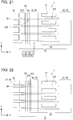
- Figs. 21 and 22 are plan views of a flow channel substrate 10 according to Embodiment 2. Features similar to those described in Embodiment 1 are represented by the same reference characters as in Embodiment 1 and are not described.
- Fig. 21 illustrates a condition observed after the diaphragm 50, the first electrode 60, the piezoelectric layer 70, the second electrode 80, and the lead electrode layer 190 are provided on the flow channel substrate 10, and the cutout portion 83 is formed.
- first lead electrodes 91 for different first electrodes 60 are not formed by patterning the lead electrode layer 190 while the cutout portion 83 is formed.
- a wiring portion 91A connected in common to all the first electrodes 60 is formed while the cutout portion 83 is formed.
- the cutout portion 83, the wiring portion 91A, and the second lead electrode 92 are each formed by patterning the lead electrode layer 190 (refer back to Fig. 14 ).
- a voltage is applied between the wiring portion 91A and the second lead electrode 92. Since the wiring portion 91A is connected to all the first electrodes 60, the voltage applied to the wiring portion 91A is also applied to all the first electrodes 60. Thus, like in Embodiment 1, the active section 310 and a part of the inactive section 320 covered with the voltage application electrode 95 are equally polarized in the same direction.
- the voltage application electrode 95 is removed, and a part of the wiring portion 91A is removed.
- the removal of the part of the wiring portion 91A forms multiple first lead electrodes 91 that are separately connected to different first electrodes 60.
- the method of manufacturing the recording head 1 according to the present embodiment can apply a voltage to all the first electrodes 60 simply by applying a voltage to the wiring portion 91A.
- a voltage can be applied to all of the first lead electrodes 91 (i.e., the first electrodes 60) at a single time through the wiring portion 91A, and the manufacturing process of the recording head 1 can be simplified accordingly.
- the voltage application electrode 95 is formed from part of the second lead electrode 92.
- the voltage application electrode 95 is formed from part of the second electrode 80.
- Figs. 23 and 24 are cross-sectional views illustrating main components of a recording head according to the present embodiment. Features similar to those described in Embodiment 1 are represented by the same reference characters as in Embodiment 1 and are not described.
- the diaphragm 50, the first electrode 60, and the piezoelectric layer 70 are provided on the flow channel substrate 10.
- a second electrode layer 180 for the second electrode 80 is formed.
- the second electrode 80 and a voltage application electrode 95A extending continuously from the second electrode 80 are formed by patterning the second electrode layer 180.
- the voltage application electrode 95A and the second electrode 80 are formed as a single piece.
- a voltage is applied between the second electrode 80 and the first electrode 60 or the conductive layer 84 that is part of the second electrode layer 180 remaining on the first electrode 60.
- This voltage application allows part of the piezoelectric layer 70 interposed between the first electrode 60 and each of the voltage application electrode 95A and the second electrode 80 to be equally polarized in the same direction.
- the voltage can be applied directly to the first electrode 60 instead of the conductive layer 84.
- the voltage application electrode 95A is removed.
- part of the inactive section 320 from which the voltage application electrode 95A has been removed and which extends continuously from the boundary with the active section 310 is polarized in the same direction as the active section 310.
- the first lead electrode 91 is formed on the first electrode 60 (the conductive layer 84), and the second lead electrode 92 is formed on the second electrode 80.
- the piezoelectric element 300 is completed.
- the method of manufacturing the recording head 1 according to the present embodiment has the same effects as those described in Embodiment 1. Further, the voltage application electrode 95A is formed as a single piece with the second electrode 80. This approach negates the need to form the voltage application electrode 95A from a material different to that of the second electrode 80, thus reducing manufacturing cost and steps. Modifications
- the method of manufacturing the recording head 1 according to Embodiments 1 to 3 forms the first electrode 60 as individual electrodes separately provided for different piezoelectric elements 300 while forming the second electrode 80 as a common electrode shared with the piezoelectric elements 300, other configurations may be used.
- the first electrode 60 may be formed as a common electrode shared with the piezoelectric elements 300 while the second electrode 80 may be formed as individual electrodes separately provided for the piezoelectric elements 300.
- multiple second lead electrodes are separately connected to individual second electrodes, and multiple voltage application electrodes, each of which extends outwardly from an end of a corresponding second lead electrode, are formed.
- Embodiment 1 can be applied to a case where the second electrode is formed as individual electrodes.
- a wiring portion connected to multiple second electrodes may be formed, and a voltage may be applied between the wiring portion and a first electrode as a common electrode, and then individual second electrodes may be formed by patterning the wiring portion.
- Embodiment 2 can be applied to a case where the second electrode is formed as individual electrodes.
- a second electrode layer for the second electrodes 80 as individual electrodes may be formed, and individual second electrodes and voltage application electrodes separately extending from the second electrodes may be formed by patterning the second electrode layer.
- Embodiment 3 can be applied to a case where the second electrode 80 is formed as individual electrodes.
- the wiring portion 91A and the second lead electrode 92 are formed by patterning the second electrode layer 180 in Embodiment 2, other configurations may be used. For example, like in Embodiment 1, after individual first lead electrodes 91 are formed, a wiring portion for connecting the first lead electrodes 91 together may be formed from a material different from that of the first lead electrodes 91. In this example, a voltage is applied between the wiring portion and the second lead electrode, and the wiring portion is then removed. This configuration also has the same effects as those described in Embodiment 1.
- the inkjet recording heads described in the above embodiments are examples of liquid ejecting heads according to an aspect of the invention, and this aspect of the invention can be applied widely to common liquid ejecting heads that may eject liquid other than ink.
- the ink jet recording apparatus described in the above embodiment is an example of liquid ejecting apparatus according to an aspect of the invention, and this aspect of the invention can be applied widely to a common liquid ejecting apparatus that may eject liquid other than ink.
- liquid ejecting heads examples include recording heads used for an image recording apparatus such as a printer, colorant ejecting heads used for manufacturing color filters in displays such as liquid crystal displays, electrode material ejecting heads used for forming electrodes in displays such as organic EL displays and field emission displays (FEDs), and bioorganic substance ejecting heads used for manufacturing biochips.
- image recording apparatus such as a printer
- colorant ejecting heads used for manufacturing color filters in displays such as liquid crystal displays
- electrode material ejecting heads used for forming electrodes in displays such as organic EL displays and field emission displays (FEDs)
- bioorganic substance ejecting heads used for manufacturing biochips.
- piezoelectric devices for liquid ejecting heads including ink jet recording heads
- some aspects of the invention can be applied to piezoelectric devices for other applications, including ultrasonic devices such as sonar devices, ultrasonic motors, pressure sensors, and pyroelectric sensors, to improve their reliability.
Landscapes
- Engineering & Computer Science (AREA)
- Manufacturing & Machinery (AREA)
- Physics & Mathematics (AREA)
- Optics & Photonics (AREA)
- Particle Formation And Scattering Control In Inkjet Printers (AREA)
- Piezo-Electric Or Mechanical Vibrators, Or Delay Or Filter Circuits (AREA)
Applications Claiming Priority (1)
| Application Number | Priority Date | Filing Date | Title |
|---|---|---|---|
| JP2016018322A JP6764126B2 (ja) | 2016-02-02 | 2016-02-02 | 圧電デバイスの製造方法 |
Publications (3)
| Publication Number | Publication Date |
|---|---|
| EP3203539A2 true EP3203539A2 (de) | 2017-08-09 |
| EP3203539A3 EP3203539A3 (de) | 2017-12-06 |
| EP3203539B1 EP3203539B1 (de) | 2023-11-29 |
Family
ID=57960296
Family Applications (1)
| Application Number | Title | Priority Date | Filing Date |
|---|---|---|---|
| EP17154121.2A Active EP3203539B1 (de) | 2016-02-02 | 2017-02-01 | Verfahren zum herstellen eines piezoelektrischen tintenstrahldruckkopfs |
Country Status (3)
| Country | Link |
|---|---|
| US (1) | US10272685B2 (de) |
| EP (1) | EP3203539B1 (de) |
| JP (1) | JP6764126B2 (de) |
Citations (1)
| Publication number | Priority date | Publication date | Assignee | Title |
|---|---|---|---|---|
| JP2006174618A (ja) | 2004-12-16 | 2006-06-29 | Kyocera Corp | 圧電アクチュエータ及び液体吐出装置 |
Family Cites Families (10)
| Publication number | Priority date | Publication date | Assignee | Title |
|---|---|---|---|---|
| US4714848A (en) | 1987-03-02 | 1987-12-22 | The United States Of America As Represented By The United States Department Of Energy | Electrically induced mechanical precompression of ferroelectric plates |
| JP2940159B2 (ja) | 1990-11-30 | 1999-08-25 | 株式会社村田製作所 | 封止型圧電部品の製造方法 |
| JP2003008379A (ja) * | 2001-06-20 | 2003-01-10 | Murata Mfg Co Ltd | エネルギー閉じ込め型圧電共振部品の製造方法 |
| US6747401B2 (en) | 2002-07-01 | 2004-06-08 | Advancewave Technology, Inc. | Augmenting surface electrode for piezoelectric workpiece |
| JP5145637B2 (ja) * | 2005-03-04 | 2013-02-20 | ソニー株式会社 | 振動型ジャイロセンサ |
| JP2009300941A (ja) * | 2008-06-17 | 2009-12-24 | Fdk Corp | 磁気光学空間光変調器の製造方法 |
| CN103026520B (zh) * | 2010-07-26 | 2015-06-17 | 富士胶片株式会社 | 形成具有弯曲压电膜的装置 |
| JP5734040B2 (ja) * | 2011-03-22 | 2015-06-10 | 京セラ株式会社 | インクジェットヘッド及び記録装置 |
| WO2013147196A1 (ja) * | 2012-03-30 | 2013-10-03 | 京セラ株式会社 | 圧電アクチュエータ、インクジェットヘッド及び圧電アクチュエータの製造方法 |
| US10352700B2 (en) | 2014-06-27 | 2019-07-16 | Sony Corporation | Gyro sensor and electronic apparatus |
-
2016
- 2016-02-02 JP JP2016018322A patent/JP6764126B2/ja active Active
-
2017
- 2017-01-30 US US15/418,882 patent/US10272685B2/en active Active
- 2017-02-01 EP EP17154121.2A patent/EP3203539B1/de active Active
Patent Citations (1)
| Publication number | Priority date | Publication date | Assignee | Title |
|---|---|---|---|---|
| JP2006174618A (ja) | 2004-12-16 | 2006-06-29 | Kyocera Corp | 圧電アクチュエータ及び液体吐出装置 |
Also Published As
| Publication number | Publication date |
|---|---|
| JP6764126B2 (ja) | 2020-09-30 |
| US20170217182A1 (en) | 2017-08-03 |
| EP3203539A3 (de) | 2017-12-06 |
| JP2017139299A (ja) | 2017-08-10 |
| EP3203539B1 (de) | 2023-11-29 |
| US10272685B2 (en) | 2019-04-30 |
Similar Documents
| Publication | Publication Date | Title |
|---|---|---|
| JP5251031B2 (ja) | 圧電素子、液体噴射ヘッド、液体噴射装置、センサー | |
| EP3347203B1 (de) | Piezoelektrische vorrichtung, flüssigkeitsausstosskopf, flüssigkeitsausstossvorrichtung und herstellungsverfahren für piezoelektrische vorrichtung | |
| JP2008284781A (ja) | 液体噴射ヘッド及びその製造方法並びに液体噴射装置 | |
| US9566790B2 (en) | Method of forming stacked wiring | |
| US20090213190A1 (en) | method of manufacturing of a liquid jet head, a method of manufacturing of a piezoelectric element and a liquid jet apparatus | |
| US8079677B2 (en) | Liquid ejecting head, liquid ejecting apparatus, and piezoelectric actuator | |
| JP4873132B2 (ja) | アクチュエータ装置の製造方法 | |
| JP5581781B2 (ja) | 圧電アクチュエーターの製造方法 | |
| US20090181329A1 (en) | Method for manufacturing a liquid jet head, a liquid jet head, and a liquid jet apparatus | |
| JP2012011558A (ja) | 液体噴射ヘッドの製造方法 | |
| US10272685B2 (en) | Method of manufacturing piezoelectric device | |
| US7887164B2 (en) | Liquid jet head, a liquid jet apparatus and a piezoelectric element | |
| JP5573251B2 (ja) | 圧電アクチュエーターの製造方法 | |
| JP5376107B2 (ja) | 圧電素子及びその製造方法、アクチュエータ装置、液体噴射ヘッド並びに液体噴射装置 | |
| JP6714827B2 (ja) | 圧電デバイス及び液体噴射ヘッド | |
| JP2017157586A (ja) | 圧電デバイスの製造方法 | |
| JP2009208411A (ja) | 液体噴射ヘッドの製造方法 | |
| JP2008205048A (ja) | 圧電素子の製造方法及び液体噴射ヘッドの製造方法 | |
| JP5256998B2 (ja) | アクチュエータ装置の製造方法及び液体噴射ヘッドの製造方法 | |
| JP4888647B2 (ja) | 液体噴射ヘッド及び液体噴射装置 | |
| JP6057071B2 (ja) | 液体噴射ヘッドの製造方法 | |
| JP5157127B2 (ja) | アクチュエータ装置及びその製造方法、並びに液体噴射ヘッド及び液体噴射装置 | |
| JP2023121050A (ja) | 圧電デバイスの製造方法および液体噴射ヘッドの製造方法 | |
| JP2016147422A (ja) | 液体噴射ヘッド、液体噴射ヘッドの製造方法、及び液体噴射装置 | |
| JP2006245248A (ja) | 圧電素子及びその製造方法、液体噴射ヘッド及びその製造方法並びに液体噴射装置 |
Legal Events
| Date | Code | Title | Description |
|---|---|---|---|
| PUAI | Public reference made under article 153(3) epc to a published international application that has entered the european phase |
Free format text: ORIGINAL CODE: 0009012 |
|
| STAA | Information on the status of an ep patent application or granted ep patent |
Free format text: STATUS: THE APPLICATION HAS BEEN PUBLISHED |
|
| AK | Designated contracting states |
Kind code of ref document: A2 Designated state(s): AL AT BE BG CH CY CZ DE DK EE ES FI FR GB GR HR HU IE IS IT LI LT LU LV MC MK MT NL NO PL PT RO RS SE SI SK SM TR |
|
| AX | Request for extension of the european patent |
Extension state: BA ME |
|
| PUAL | Search report despatched |
Free format text: ORIGINAL CODE: 0009013 |
|
| AK | Designated contracting states |
Kind code of ref document: A3 Designated state(s): AL AT BE BG CH CY CZ DE DK EE ES FI FR GB GR HR HU IE IS IT LI LT LU LV MC MK MT NL NO PL PT RO RS SE SI SK SM TR |
|
| AX | Request for extension of the european patent |
Extension state: BA ME |
|
| RIC1 | Information provided on ipc code assigned before grant |
Ipc: H01L 41/257 20130101ALI20171030BHEP Ipc: H01L 41/253 20130101AFI20171030BHEP |
|
| STAA | Information on the status of an ep patent application or granted ep patent |
Free format text: STATUS: REQUEST FOR EXAMINATION WAS MADE |
|
| 17P | Request for examination filed |
Effective date: 20180420 |
|
| RBV | Designated contracting states (corrected) |
Designated state(s): AL AT BE BG CH CY CZ DE DK EE ES FI FR GB GR HR HU IE IS IT LI LT LU LV MC MK MT NL NO PL PT RO RS SE SI SK SM TR |
|
| STAA | Information on the status of an ep patent application or granted ep patent |
Free format text: STATUS: EXAMINATION IS IN PROGRESS |
|
| 17Q | First examination report despatched |
Effective date: 20210412 |
|
| REG | Reference to a national code |
Ref country code: DE Ref legal event code: R079 Free format text: PREVIOUS MAIN CLASS: H01L0041253000 Ipc: H10N0030045000 Ref country code: DE Ref legal event code: R079 Ref document number: 602017076920 Country of ref document: DE Free format text: PREVIOUS MAIN CLASS: H01L0041253000 Ipc: H10N0030045000 |
|
| REG | Reference to a national code |
Ref country code: DE Ref legal event code: R079 Free format text: PREVIOUS MAIN CLASS: H10N0030045000 Ipc: B41J0002160000 Ref country code: DE Ref legal event code: R079 Ref document number: 602017076920 Country of ref document: DE Free format text: PREVIOUS MAIN CLASS: H10N0030045000 Ipc: B41J0002160000 |
|
| REG | Reference to a national code |
Ref country code: DE Ref legal event code: R079 Free format text: PREVIOUS MAIN CLASS: B41J0002160000 Ipc: H10N0030200000 Ref country code: DE Ref legal event code: R079 Ref document number: 602017076920 Country of ref document: DE Free format text: PREVIOUS MAIN CLASS: B41J0002160000 Ipc: H10N0030200000 |
|
| RIC1 | Information provided on ipc code assigned before grant |
Ipc: H10N 30/20 20230101ALI20230515BHEP Ipc: H10N 30/045 20230101AFI20230515BHEP |
|
| GRAP | Despatch of communication of intention to grant a patent |
Free format text: ORIGINAL CODE: EPIDOSNIGR1 |
|
| STAA | Information on the status of an ep patent application or granted ep patent |
Free format text: STATUS: GRANT OF PATENT IS INTENDED |
|
| RIC1 | Information provided on ipc code assigned before grant |
Ipc: B41J 2/16 20060101AFI20230526BHEP |
|
| RIC1 | Information provided on ipc code assigned before grant |
Ipc: B41J 2/16 20060101ALI20230602BHEP Ipc: H10N 30/045 20230101ALI20230602BHEP Ipc: H10N 30/20 20230101AFI20230602BHEP |
|
| INTG | Intention to grant announced |
Effective date: 20230623 |
|
| GRAS | Grant fee paid |
Free format text: ORIGINAL CODE: EPIDOSNIGR3 |
|
| GRAA | (expected) grant |
Free format text: ORIGINAL CODE: 0009210 |
|
| STAA | Information on the status of an ep patent application or granted ep patent |
Free format text: STATUS: THE PATENT HAS BEEN GRANTED |
|
| AK | Designated contracting states |
Kind code of ref document: B1 Designated state(s): AL AT BE BG CH CY CZ DE DK EE ES FI FR GB GR HR HU IE IS IT LI LT LU LV MC MK MT NL NO PL PT RO RS SE SI SK SM TR |
|
| REG | Reference to a national code |
Ref country code: GB Ref legal event code: FG4D |
|
| REG | Reference to a national code |
Ref country code: CH Ref legal event code: EP |
|
| REG | Reference to a national code |
Ref country code: DE Ref legal event code: R096 Ref document number: 602017076920 Country of ref document: DE |
|
| REG | Reference to a national code |
Ref country code: IE Ref legal event code: FG4D |
|
| REG | Reference to a national code |
Ref country code: LT Ref legal event code: MG9D |
|
| REG | Reference to a national code |
Ref country code: NL Ref legal event code: MP Effective date: 20231129 |
|
| PG25 | Lapsed in a contracting state [announced via postgrant information from national office to epo] |
Ref country code: GR Free format text: LAPSE BECAUSE OF FAILURE TO SUBMIT A TRANSLATION OF THE DESCRIPTION OR TO PAY THE FEE WITHIN THE PRESCRIBED TIME-LIMIT Effective date: 20240301 |
|
| PG25 | Lapsed in a contracting state [announced via postgrant information from national office to epo] |
Ref country code: IS Free format text: LAPSE BECAUSE OF FAILURE TO SUBMIT A TRANSLATION OF THE DESCRIPTION OR TO PAY THE FEE WITHIN THE PRESCRIBED TIME-LIMIT Effective date: 20240329 |
|
| PG25 | Lapsed in a contracting state [announced via postgrant information from national office to epo] |
Ref country code: LT Free format text: LAPSE BECAUSE OF FAILURE TO SUBMIT A TRANSLATION OF THE DESCRIPTION OR TO PAY THE FEE WITHIN THE PRESCRIBED TIME-LIMIT Effective date: 20231129 |
|
| PG25 | Lapsed in a contracting state [announced via postgrant information from national office to epo] |
Ref country code: ES Free format text: LAPSE BECAUSE OF FAILURE TO SUBMIT A TRANSLATION OF THE DESCRIPTION OR TO PAY THE FEE WITHIN THE PRESCRIBED TIME-LIMIT Effective date: 20231129 |
|
| PG25 | Lapsed in a contracting state [announced via postgrant information from national office to epo] |
Ref country code: LT Free format text: LAPSE BECAUSE OF FAILURE TO SUBMIT A TRANSLATION OF THE DESCRIPTION OR TO PAY THE FEE WITHIN THE PRESCRIBED TIME-LIMIT Effective date: 20231129 Ref country code: IS Free format text: LAPSE BECAUSE OF FAILURE TO SUBMIT A TRANSLATION OF THE DESCRIPTION OR TO PAY THE FEE WITHIN THE PRESCRIBED TIME-LIMIT Effective date: 20240329 Ref country code: GR Free format text: LAPSE BECAUSE OF FAILURE TO SUBMIT A TRANSLATION OF THE DESCRIPTION OR TO PAY THE FEE WITHIN THE PRESCRIBED TIME-LIMIT Effective date: 20240301 Ref country code: ES Free format text: LAPSE BECAUSE OF FAILURE TO SUBMIT A TRANSLATION OF THE DESCRIPTION OR TO PAY THE FEE WITHIN THE PRESCRIBED TIME-LIMIT Effective date: 20231129 Ref country code: BG Free format text: LAPSE BECAUSE OF FAILURE TO SUBMIT A TRANSLATION OF THE DESCRIPTION OR TO PAY THE FEE WITHIN THE PRESCRIBED TIME-LIMIT Effective date: 20240229 |
|
| REG | Reference to a national code |
Ref country code: AT Ref legal event code: MK05 Ref document number: 1637469 Country of ref document: AT Kind code of ref document: T Effective date: 20231129 |
|
| PG25 | Lapsed in a contracting state [announced via postgrant information from national office to epo] |
Ref country code: NL Free format text: LAPSE BECAUSE OF FAILURE TO SUBMIT A TRANSLATION OF THE DESCRIPTION OR TO PAY THE FEE WITHIN THE PRESCRIBED TIME-LIMIT Effective date: 20231129 |
|
| PG25 | Lapsed in a contracting state [announced via postgrant information from national office to epo] |
Ref country code: SE Free format text: LAPSE BECAUSE OF FAILURE TO SUBMIT A TRANSLATION OF THE DESCRIPTION OR TO PAY THE FEE WITHIN THE PRESCRIBED TIME-LIMIT Effective date: 20231129 Ref country code: RS Free format text: LAPSE BECAUSE OF FAILURE TO SUBMIT A TRANSLATION OF THE DESCRIPTION OR TO PAY THE FEE WITHIN THE PRESCRIBED TIME-LIMIT Effective date: 20231129 Ref country code: PL Free format text: LAPSE BECAUSE OF FAILURE TO SUBMIT A TRANSLATION OF THE DESCRIPTION OR TO PAY THE FEE WITHIN THE PRESCRIBED TIME-LIMIT Effective date: 20231129 Ref country code: NO Free format text: LAPSE BECAUSE OF FAILURE TO SUBMIT A TRANSLATION OF THE DESCRIPTION OR TO PAY THE FEE WITHIN THE PRESCRIBED TIME-LIMIT Effective date: 20240229 Ref country code: NL Free format text: LAPSE BECAUSE OF FAILURE TO SUBMIT A TRANSLATION OF THE DESCRIPTION OR TO PAY THE FEE WITHIN THE PRESCRIBED TIME-LIMIT Effective date: 20231129 Ref country code: LV Free format text: LAPSE BECAUSE OF FAILURE TO SUBMIT A TRANSLATION OF THE DESCRIPTION OR TO PAY THE FEE WITHIN THE PRESCRIBED TIME-LIMIT Effective date: 20231129 Ref country code: HR Free format text: LAPSE BECAUSE OF FAILURE TO SUBMIT A TRANSLATION OF THE DESCRIPTION OR TO PAY THE FEE WITHIN THE PRESCRIBED TIME-LIMIT Effective date: 20231129 |
|
| PG25 | Lapsed in a contracting state [announced via postgrant information from national office to epo] |
Ref country code: DK Free format text: LAPSE BECAUSE OF FAILURE TO SUBMIT A TRANSLATION OF THE DESCRIPTION OR TO PAY THE FEE WITHIN THE PRESCRIBED TIME-LIMIT Effective date: 20231129 |
|
| PG25 | Lapsed in a contracting state [announced via postgrant information from national office to epo] |
Ref country code: AT Free format text: LAPSE BECAUSE OF FAILURE TO SUBMIT A TRANSLATION OF THE DESCRIPTION OR TO PAY THE FEE WITHIN THE PRESCRIBED TIME-LIMIT Effective date: 20231129 Ref country code: CZ Free format text: LAPSE BECAUSE OF FAILURE TO SUBMIT A TRANSLATION OF THE DESCRIPTION OR TO PAY THE FEE WITHIN THE PRESCRIBED TIME-LIMIT Effective date: 20231129 |
|
| PG25 | Lapsed in a contracting state [announced via postgrant information from national office to epo] |
Ref country code: SK Free format text: LAPSE BECAUSE OF FAILURE TO SUBMIT A TRANSLATION OF THE DESCRIPTION OR TO PAY THE FEE WITHIN THE PRESCRIBED TIME-LIMIT Effective date: 20231129 |
|
| PG25 | Lapsed in a contracting state [announced via postgrant information from national office to epo] |
Ref country code: SM Free format text: LAPSE BECAUSE OF FAILURE TO SUBMIT A TRANSLATION OF THE DESCRIPTION OR TO PAY THE FEE WITHIN THE PRESCRIBED TIME-LIMIT Effective date: 20231129 Ref country code: SK Free format text: LAPSE BECAUSE OF FAILURE TO SUBMIT A TRANSLATION OF THE DESCRIPTION OR TO PAY THE FEE WITHIN THE PRESCRIBED TIME-LIMIT Effective date: 20231129 Ref country code: RO Free format text: LAPSE BECAUSE OF FAILURE TO SUBMIT A TRANSLATION OF THE DESCRIPTION OR TO PAY THE FEE WITHIN THE PRESCRIBED TIME-LIMIT Effective date: 20231129 Ref country code: IT Free format text: LAPSE BECAUSE OF FAILURE TO SUBMIT A TRANSLATION OF THE DESCRIPTION OR TO PAY THE FEE WITHIN THE PRESCRIBED TIME-LIMIT Effective date: 20231129 Ref country code: EE Free format text: LAPSE BECAUSE OF FAILURE TO SUBMIT A TRANSLATION OF THE DESCRIPTION OR TO PAY THE FEE WITHIN THE PRESCRIBED TIME-LIMIT Effective date: 20231129 Ref country code: DK Free format text: LAPSE BECAUSE OF FAILURE TO SUBMIT A TRANSLATION OF THE DESCRIPTION OR TO PAY THE FEE WITHIN THE PRESCRIBED TIME-LIMIT Effective date: 20231129 Ref country code: CZ Free format text: LAPSE BECAUSE OF FAILURE TO SUBMIT A TRANSLATION OF THE DESCRIPTION OR TO PAY THE FEE WITHIN THE PRESCRIBED TIME-LIMIT Effective date: 20231129 Ref country code: AT Free format text: LAPSE BECAUSE OF FAILURE TO SUBMIT A TRANSLATION OF THE DESCRIPTION OR TO PAY THE FEE WITHIN THE PRESCRIBED TIME-LIMIT Effective date: 20231129 |
|
| PG25 | Lapsed in a contracting state [announced via postgrant information from national office to epo] |
Ref country code: PT Free format text: LAPSE BECAUSE OF FAILURE TO SUBMIT A TRANSLATION OF THE DESCRIPTION OR TO PAY THE FEE WITHIN THE PRESCRIBED TIME-LIMIT Effective date: 20240401 |
|
| PG25 | Lapsed in a contracting state [announced via postgrant information from national office to epo] |
Ref country code: PT Free format text: LAPSE BECAUSE OF FAILURE TO SUBMIT A TRANSLATION OF THE DESCRIPTION OR TO PAY THE FEE WITHIN THE PRESCRIBED TIME-LIMIT Effective date: 20240401 |
|
| REG | Reference to a national code |
Ref country code: DE Ref legal event code: R097 Ref document number: 602017076920 Country of ref document: DE |
|
| REG | Reference to a national code |
Ref country code: DE Ref legal event code: R119 Ref document number: 602017076920 Country of ref document: DE |
|
| PG25 | Lapsed in a contracting state [announced via postgrant information from national office to epo] |
Ref country code: MC Free format text: LAPSE BECAUSE OF FAILURE TO SUBMIT A TRANSLATION OF THE DESCRIPTION OR TO PAY THE FEE WITHIN THE PRESCRIBED TIME-LIMIT Effective date: 20231129 |
|
| REG | Reference to a national code |
Ref country code: CH Ref legal event code: PL |
|
| PLBE | No opposition filed within time limit |
Free format text: ORIGINAL CODE: 0009261 |
|
| STAA | Information on the status of an ep patent application or granted ep patent |
Free format text: STATUS: NO OPPOSITION FILED WITHIN TIME LIMIT |
|
| PG25 | Lapsed in a contracting state [announced via postgrant information from national office to epo] |
Ref country code: LU Free format text: LAPSE BECAUSE OF NON-PAYMENT OF DUE FEES Effective date: 20240201 |
|
| PG25 | Lapsed in a contracting state [announced via postgrant information from national office to epo] |
Ref country code: CH Free format text: LAPSE BECAUSE OF NON-PAYMENT OF DUE FEES Effective date: 20240229 |
|
| PG25 | Lapsed in a contracting state [announced via postgrant information from national office to epo] |
Ref country code: SI Free format text: LAPSE BECAUSE OF FAILURE TO SUBMIT A TRANSLATION OF THE DESCRIPTION OR TO PAY THE FEE WITHIN THE PRESCRIBED TIME-LIMIT Effective date: 20231129 |
|
| PG25 | Lapsed in a contracting state [announced via postgrant information from national office to epo] |
Ref country code: SI Free format text: LAPSE BECAUSE OF FAILURE TO SUBMIT A TRANSLATION OF THE DESCRIPTION OR TO PAY THE FEE WITHIN THE PRESCRIBED TIME-LIMIT Effective date: 20231129 Ref country code: LU Free format text: LAPSE BECAUSE OF NON-PAYMENT OF DUE FEES Effective date: 20240201 Ref country code: CH Free format text: LAPSE BECAUSE OF NON-PAYMENT OF DUE FEES Effective date: 20240229 |
|
| 26N | No opposition filed |
Effective date: 20240830 |
|
| REG | Reference to a national code |
Ref country code: BE Ref legal event code: MM Effective date: 20240229 |
|
| PG25 | Lapsed in a contracting state [announced via postgrant information from national office to epo] |
Ref country code: DE Free format text: LAPSE BECAUSE OF NON-PAYMENT OF DUE FEES Effective date: 20240903 |
|
| PG25 | Lapsed in a contracting state [announced via postgrant information from national office to epo] |
Ref country code: BE Free format text: LAPSE BECAUSE OF NON-PAYMENT OF DUE FEES Effective date: 20240229 |
|
| PG25 | Lapsed in a contracting state [announced via postgrant information from national office to epo] |
Ref country code: FR Free format text: LAPSE BECAUSE OF NON-PAYMENT OF DUE FEES Effective date: 20240229 |
|
| PG25 | Lapsed in a contracting state [announced via postgrant information from national office to epo] |
Ref country code: IE Free format text: LAPSE BECAUSE OF NON-PAYMENT OF DUE FEES Effective date: 20240201 |
|
| PG25 | Lapsed in a contracting state [announced via postgrant information from national office to epo] |
Ref country code: IE Free format text: LAPSE BECAUSE OF NON-PAYMENT OF DUE FEES Effective date: 20240201 Ref country code: FR Free format text: LAPSE BECAUSE OF NON-PAYMENT OF DUE FEES Effective date: 20240229 Ref country code: DE Free format text: LAPSE BECAUSE OF NON-PAYMENT OF DUE FEES Effective date: 20240903 Ref country code: BE Free format text: LAPSE BECAUSE OF NON-PAYMENT OF DUE FEES Effective date: 20240229 |
|
| PG25 | Lapsed in a contracting state [announced via postgrant information from national office to epo] |
Ref country code: CY Free format text: LAPSE BECAUSE OF FAILURE TO SUBMIT A TRANSLATION OF THE DESCRIPTION OR TO PAY THE FEE WITHIN THE PRESCRIBED TIME-LIMIT; INVALID AB INITIO Effective date: 20170201 |
|
| PG25 | Lapsed in a contracting state [announced via postgrant information from national office to epo] |
Ref country code: HU Free format text: LAPSE BECAUSE OF FAILURE TO SUBMIT A TRANSLATION OF THE DESCRIPTION OR TO PAY THE FEE WITHIN THE PRESCRIBED TIME-LIMIT; INVALID AB INITIO Effective date: 20170201 |
|
| PG25 | Lapsed in a contracting state [announced via postgrant information from national office to epo] |
Ref country code: FI Free format text: LAPSE BECAUSE OF FAILURE TO SUBMIT A TRANSLATION OF THE DESCRIPTION OR TO PAY THE FEE WITHIN THE PRESCRIBED TIME-LIMIT Effective date: 20231129 |
|
| PG25 | Lapsed in a contracting state [announced via postgrant information from national office to epo] |
Ref country code: TR Free format text: LAPSE BECAUSE OF FAILURE TO SUBMIT A TRANSLATION OF THE DESCRIPTION OR TO PAY THE FEE WITHIN THE PRESCRIBED TIME-LIMIT Effective date: 20231129 |
|
| PGFP | Annual fee paid to national office [announced via postgrant information from national office to epo] |
Ref country code: GB Payment date: 20260219 Year of fee payment: 10 |