EP3197045B1 - Curve fitting circuit, analog predistorter and radio frequency signal transmitter - Google Patents
Curve fitting circuit, analog predistorter and radio frequency signal transmitter Download PDFInfo
- Publication number
- EP3197045B1 EP3197045B1 EP14904793.8A EP14904793A EP3197045B1 EP 3197045 B1 EP3197045 B1 EP 3197045B1 EP 14904793 A EP14904793 A EP 14904793A EP 3197045 B1 EP3197045 B1 EP 3197045B1
- Authority
- EP
- European Patent Office
- Prior art keywords
- circuit
- signal
- amplitude
- output
- segmentation processing
- Prior art date
- Legal status (The legal status is an assumption and is not a legal conclusion. Google has not performed a legal analysis and makes no representation as to the accuracy of the status listed.)
- Active
Links
- 238000012545 processing Methods 0.000 claims description 116
- 230000011218 segmentation Effects 0.000 claims description 111
- 238000000034 method Methods 0.000 claims description 34
- 238000013507 mapping Methods 0.000 claims description 8
- 230000006870 function Effects 0.000 description 15
- 238000010586 diagram Methods 0.000 description 14
- 238000013139 quantization Methods 0.000 description 8
- 238000004590 computer program Methods 0.000 description 7
- 238000000354 decomposition reaction Methods 0.000 description 6
- 238000006243 chemical reaction Methods 0.000 description 4
- 238000012986 modification Methods 0.000 description 4
- 230000004048 modification Effects 0.000 description 4
- 230000003321 amplification Effects 0.000 description 3
- 238000004891 communication Methods 0.000 description 3
- 230000003247 decreasing effect Effects 0.000 description 3
- 238000003199 nucleic acid amplification method Methods 0.000 description 3
- 230000007423 decrease Effects 0.000 description 2
- 238000005516 engineering process Methods 0.000 description 2
- 230000009286 beneficial effect Effects 0.000 description 1
- 238000013461 design Methods 0.000 description 1
- 230000008030 elimination Effects 0.000 description 1
- 238000003379 elimination reaction Methods 0.000 description 1
- 230000003287 optical effect Effects 0.000 description 1
Images


Classifications
-
- H—ELECTRICITY
- H03—ELECTRONIC CIRCUITRY
- H03F—AMPLIFIERS
- H03F1/00—Details of amplifiers with only discharge tubes, only semiconductor devices or only unspecified devices as amplifying elements
- H03F1/26—Modifications of amplifiers to reduce influence of noise generated by amplifying elements
-
- H—ELECTRICITY
- H03—ELECTRONIC CIRCUITRY
- H03F—AMPLIFIERS
- H03F1/00—Details of amplifiers with only discharge tubes, only semiconductor devices or only unspecified devices as amplifying elements
- H03F1/32—Modifications of amplifiers to reduce non-linear distortion
- H03F1/3241—Modifications of amplifiers to reduce non-linear distortion using predistortion circuits
- H03F1/3247—Modifications of amplifiers to reduce non-linear distortion using predistortion circuits using feedback acting on predistortion circuits
-
- G—PHYSICS
- G06—COMPUTING; CALCULATING OR COUNTING
- G06F—ELECTRIC DIGITAL DATA PROCESSING
- G06F17/00—Digital computing or data processing equipment or methods, specially adapted for specific functions
- G06F17/10—Complex mathematical operations
-
- G—PHYSICS
- G06—COMPUTING; CALCULATING OR COUNTING
- G06F—ELECTRIC DIGITAL DATA PROCESSING
- G06F17/00—Digital computing or data processing equipment or methods, specially adapted for specific functions
- G06F17/10—Complex mathematical operations
- G06F17/17—Function evaluation by approximation methods, e.g. inter- or extrapolation, smoothing, least mean square method
-
- H—ELECTRICITY
- H03—ELECTRONIC CIRCUITRY
- H03F—AMPLIFIERS
- H03F1/00—Details of amplifiers with only discharge tubes, only semiconductor devices or only unspecified devices as amplifying elements
- H03F1/32—Modifications of amplifiers to reduce non-linear distortion
- H03F1/3241—Modifications of amplifiers to reduce non-linear distortion using predistortion circuits
- H03F1/3258—Modifications of amplifiers to reduce non-linear distortion using predistortion circuits based on polynomial terms
-
- H—ELECTRICITY
- H03—ELECTRONIC CIRCUITRY
- H03F—AMPLIFIERS
- H03F3/00—Amplifiers with only discharge tubes or only semiconductor devices as amplifying elements
- H03F3/189—High-frequency amplifiers, e.g. radio frequency amplifiers
-
- H—ELECTRICITY
- H03—ELECTRONIC CIRCUITRY
- H03F—AMPLIFIERS
- H03F3/00—Amplifiers with only discharge tubes or only semiconductor devices as amplifying elements
- H03F3/189—High-frequency amplifiers, e.g. radio frequency amplifiers
- H03F3/19—High-frequency amplifiers, e.g. radio frequency amplifiers with semiconductor devices only
-
- H—ELECTRICITY
- H03—ELECTRONIC CIRCUITRY
- H03F—AMPLIFIERS
- H03F3/00—Amplifiers with only discharge tubes or only semiconductor devices as amplifying elements
- H03F3/20—Power amplifiers, e.g. Class B amplifiers, Class C amplifiers
-
- H—ELECTRICITY
- H03—ELECTRONIC CIRCUITRY
- H03F—AMPLIFIERS
- H03F3/00—Amplifiers with only discharge tubes or only semiconductor devices as amplifying elements
- H03F3/20—Power amplifiers, e.g. Class B amplifiers, Class C amplifiers
- H03F3/24—Power amplifiers, e.g. Class B amplifiers, Class C amplifiers of transmitter output stages
- H03F3/245—Power amplifiers, e.g. Class B amplifiers, Class C amplifiers of transmitter output stages with semiconductor devices only
-
- H—ELECTRICITY
- H03—ELECTRONIC CIRCUITRY
- H03F—AMPLIFIERS
- H03F2200/00—Indexing scheme relating to amplifiers
- H03F2200/102—A non-specified detector of a signal envelope being used in an amplifying circuit
-
- H—ELECTRICITY
- H03—ELECTRONIC CIRCUITRY
- H03F—AMPLIFIERS
- H03F2200/00—Indexing scheme relating to amplifiers
- H03F2200/451—Indexing scheme relating to amplifiers the amplifier being a radio frequency amplifier
Definitions
- the present invention relates to the field of communications technologies, and in particular, to a curve fitting circuit, an analog predistorter, and a radio frequency signal transmitter.
- a multi-input radio frequency power amplifier is a power amplifier that has two or more radio frequency signal input ends and a single output end. Compared with a conventional single-input single-output radio frequency power amplifier, the multi-input radio frequency power amplifier has better performance. In addition, a relationship between amplitude and a phase of each input signal of the multi-input radio frequency power amplifier can be adjusted. Therefore, the multi-input radio frequency power amplifier has better performance, and the multi-input radio frequency power amplifier attracts more attention.
- the document US 2011/0053532 A1 shows a radio communication device and a radio communication method using an envelope tracking system ET and an envelope elimination and envelope restoration system EER.
- a conversion curve (Pout-Vds curve) indicating a relation between an envelope of a transmit signal and a drain voltage applied in an operation of an ET system is determined on the basis of a relation between an output power and an efficiency attained at each drain voltage of a power amplifier by dividing an amplitude range of the envelope signal on the conversion curve into a plurality of sections and determining the polynomial series of at least one section to approximate the drain voltage.
- a conventional transmitter using a multi-input power amplifier requires at least two complete radio frequency small-signal links. In this case, a quantity of small-signal paths increases in the transmitter, and a structure of the transmitter becomes complex.
- a radio frequency signal decomposition solution is generally used in a current transmitter.
- the structure of the transmitter in which the radio frequency signal decomposition solution is used may be shown in FIG. 1 :
- a signal component splitting module 15 receives a signal output by a quadrature modulator 14, decomposes the received signal into two channels of signals, and outputs the signals into two drive amplifiers 16.
- the transmitter shown in FIG. 1 further includes a digital predistortion module 11, a quadrature modulation compensation module 12, a digital-to-analog conversion module 13, a radio frequency power amplifier 17, a down-converter 18, and an analog-to-digital conversion module 19.
- the signal component splitting module includes an envelope detector 21, a quadrature signal splitter 22, a multiplier 23, and a curve fitting circuit 24.
- a design of the curve fitting circuit 24 is a key in the signal component splitting module, and a function of the curve fitting circuit is to convert an input signal represented by a real number into an output signal represented by a complex number.
- the curve fitting circuit implements mathematical computation by using a circuit. Therefore, an error is unavoidable, and this requires that a circuit structure features a particular tolerance.
- the signal component splitting module implementing a radio frequency signal decomposition function needs to fit a relatively complex curve.
- a higher order polynomial needs to be used.
- a fitting result is very sensitive to a higher order term coefficient, that is, a higher order coefficient.
- the fitting result is also very sensitive to a quantization noise.
- a curve that needs to be fit during radio frequency signal decomposition is relatively complex, and a higher order polynomial is generally used when a current polynomial fitting method is used. Therefore, a fitting result is not only very sensitive to a higher order term coefficient, but also very sensitive to a quantization noise.
- Embodiments of the present invention provide a curve fitting circuit, an analog predistorter and a radio frequency signal transmitter, so as to resolve a problem that, when radio frequency signal decomposition is performed by using an existing polynomial fitting method, a fitting result caused by frequent use of a higher order polynomial is very sensitive to both a higher order term coefficient and a quantization noise.
- a curve fitting circuit configured to receive an input signal, connect to a power amplifier and provide q output signals to the power amplifier, including n segmentation processing circuits and q first adder circuits, where n is greater than or equal to 2, and q is a natural number; each segmentation processing circuit receives the input signal, intercepts a part of the input signal according to a preset rule, generates a to-be-processed signal according to the intercepted part, and generates q output signals according to the to-be-processed signal by using a polynomial fitting method, where parts intercepted by different segmentation processing circuits are not exactly the same; and each first adder circuit receives one signal of the q output signals of each segmentation processing circuit, adds n received signals, and obtains one output signal as one output signal of the q output signals of the curve fitting circuit according to a sum of received n signals, where different first adder circuits receive different output signals from one segmentation processing
- each first adder circuit is specifically configured to: receive one signal from each segmentation processing circuit; and when none of the q output signals of each segmentation processing circuit includes a constant term, use a signal, obtained by adding result of adding the n received signals to a constant term, as one output signal of the q output signals of the curve fitting circuit, or when q output signals of at least one segmentation processing circuit include a constant term, use result of adding the n received signals as one output signal of the curve fitting circuit.
- each segmentation processing circuit is specifically configured to: receive an input signal, determine an intercepted part according to an amplitude of the input signal and a preset amplitude range of the segmentation processing circuit, generate a to-be-processed signal according to the intercepted part, and generate q output signals according to the to-be-processed signal by using the polynomial fitting method.
- each segmentation processing circuit is specifically configured to: receive an input signal, intercept a part between two points of the input signal, generate a to-be-processed signal according to the intercepted part, and generate q output signals according to the to-be-processed signal by using the polynomial fitting method.
- the amplitude limiting circuit includes a pre-adjustment circuit and an amplitude limiting amplifier circuit, where the pre-adjustment circuit receives the input signal and outputs a signal obtained by amplifying the input signal and/or performing offset adjustment on the input signal; and the amplitude limiting amplifier circuit receives the signal output by the pre-adjustment circuit; and generates and outputs, when an amplitude of the signal output by the pre-adjustment circuit is within an amplitude limiting range of the amplitude limiting amplifier circuit, the to-be-processed signal whose amplitude monotonically varies according to the amplitude of the signal output by the pre-adjustment circuit, or outputs the first preset value when the amplitude of the signal output by the pre-adjustment circuit is less than a minimum value of the amplitude limiting range of the amplitude limiting amplifier circuit, or outputs the second preset value when the amplitude of the signal output
- the amplitude limiting amplifier circuit includes a first triode, a second triode, a third triode, a fourth triode, a first resistor, a second resistor, a third resistor, a fourth resistor, a fifth resistor, a sixth resistor, and a seventh resistor, where one end of the first resistor receives an amplitude-limited signal, the other end of the first resistor is separately connected to a collector of the first triode, a base of the first triode, and a base of the second triode, an emitter of the first triode is grounded by using the second resistor, an emitter of the second triode is grounded by using the third resistor, and a collector of the second triode outputs a signal related to an amplitude of the amplitude-limited signal; a base of the third triode receives a first input signal, a base of the fourth triode receives a second input signal, a collector of the
- the preset order is m
- the preset order is m
- an analog predistorter including a curve fitting circuit provided in the embodiments of the present invention.
- a radio frequency signal transmitter including a curve fitting circuit provided in the embodiments of the present invention.
- each segmentation processing circuit in the curve fitting circuit intercepts a part of an input signal, and each segmentation processing circuit fits only the part intercepted by the segmentation processing circuit.
- each segmentation processing circuit generates an output signal according to only a part of signal in the input signal by using a polynomial fitting method, a highest order of basis functions in a used polynomial is reduced. This makes an output signal of each segmentation processing circuit less sensitive to both a higher order term coefficient and a quantization noise, thereby making an output signal of the curve fitting circuit less sensitive to both the higher order term coefficient and the quantization noise.
- Embodiments of the present invention provide a curve fitting circuit, an analog predistorter, and a radio frequency signal transmitter.
- Each segmentation processing circuit in the curve fitting circuit generates q output signals according to only a part of an input signal by using a polynomial fitting method. After the input signal is divided into n parts, complexity of each part of signal is greatly reduced. Therefore, when each segmentation processing circuit uses a polynomial fitting method, a highest order of basis functions in a used polynomial is reduced. This makes an output signal of each segmentation processing circuit less sensitive to both a higher order term coefficient and a quantization noise, thereby making an output signal of the curve fitting circuit less sensitive to both the higher order term coefficient and the quantization noise.
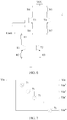
- An embodiment of the present invention provides a curve fitting circuit, as shown in FIG. 3 , including n segmentation processing circuits 31 and q first adder circuits 32, where n is greater than or equal to 2, and q is a natural number.
- Each segmentation processing circuit 31 receives an input signal, intercepts a part of the input signal according to a preset rule, generates a to-be-processed signal according to the intercepted part, and generates q output signals according to the to-be-processed signal by using a polynomial fitting method, where parts intercepted by different segmentation processing circuits are not exactly the same.
- Each first adder circuit 32 is configured to: receive one signal in the q output signals of each segmentation processing circuit 31, and obtain one output signal of the curve fitting circuit according to a sum of received n signals, where different first adder circuits 32 receive different output signals in q output signals of a same segmentation processing circuit 31.
- the capturing a part of the input signal according to the preset rule may be capturing a part of the input signal whose amplitude is within a preset amplitude range of the segmentation processing circuit, or may be capturing a part between two points of the input signal, or may be capturing the input signal according to another feature of the input signal.
- a signal A is fit to obtain a signal B.
- target accuracy can be reached. That is, the basis functions in the to-be-used polynomial are respectively x 5 , x 4 , x 3 , x 2 , x 1 and x 0 .
- a complexity degree of each part of signal is lower than a complexity degree of the signal A.
- the target accuracy can be reached when the highest order of the basis functions in the to-be-used polynomial is less than 5.
- the signal A is divided into several parts, when fitting is performed according to each part by using the polynomial fitting method, a fitting result is less sensitive to both a higher order coefficient and a quantization noise are reduced.
- each segmentation processing circuit If only one curve needs to be fit, for example, a real signal is fit to obtain a real signal, each segmentation processing circuit generates only one output signal. After a first adder circuit 32 adds the output signal of each segmentation processing circuit, an output signal of the curve fitting circuit provided in this embodiment of the present invention is obtained, and the curve fitting circuit has only one output signal.
- each segmentation processing circuit needs to generate two output signals. After receiving one output signal of each segmentation processing circuit, a first adder circuit adds received n output signals and obtains one output signal of the curve fitting circuit; and after receiving one output signal of each segmentation processing circuit, the other first adder circuit adds received n output signals and obtains the other output signal of the curve fitting circuit.
- the two first adder circuits receive different output signals in two output signals of a same segmentation processing circuit.
- One output signal of the curve fitting circuit is a real part of the complex signal, and the other output signal of the curve fitting circuit is an imaginary part of the complex signal.
- each segmentation processing circuit needs to generate q output signals.
- Each first adder circuit receives one signal in the q signals output by each segmentation processing circuit, and uses a signal, obtained by adding received n signals, as one output signal of the curve fitting circuit.
- Different first adder circuits receive different output signals in q output signals of a same segmentation processing circuit, so as to obtain q output signals of the curve fitting circuit.
- each first adder circuit is specifically configured to: receive one signal in the q output signals output by each segmentation processing circuit; and when none of the q output signals of each segmentation processing circuit includes a constant term, use a signal, obtained by adding the sum of the received n signals to a constant term, as one output signal of the curve fitting circuit, or when q output signals of at least one segmentation processing circuit include a constant term, use the sum of the received n signals as one output signal of the curve fitting circuit.
- each segmentation processing circuit when each segmentation processing circuit generates the output signals according to the to-be-processed signal by using the polynomial fitting method, and when a used polynomial includes no constant term (that is, a constant), after adding the received n signals, each first adder circuit further needs to add a constant, and uses a signal, obtained by adding the constant, as one output signal of the curve fitting circuit.
- each first adder circuit may add only the received n signals and use the sum as one output signal of the curve fitting circuit.
- each segmentation processing circuit is specifically configured to: receive an input signal, intercept a part between two points of the input signal, generate a to-be-processed signal according to the intercepted part, and generate q output signals according to the to-be-processed signal by using the polynomial fitting method.
- the input signal may be segmented at an inflection point, or the input signal may be segmented at any other point.
- An inflection point of the input signal is a point at which a slope change rate of the input signal is greater than a preset value.
- a curve fitting circuit includes three segmentation processing circuits, and inflection points of an input signal are x1, x2, x3, x4, and x5, where x1 ⁇ x2 ⁇ x3 ⁇ x4 ⁇ x5.
- a first segmentation processing circuit in the three segmentation processing circuits processes only a part between x1 and x3 of the input signal
- a second segmentation processing circuit in the three segmentation processing circuits processes only a part between x2 and x4 of the input signal
- a third segmentation processing circuit in the three segmentation processing circuits processes only a part between x3 and x5 of the input signal.
- each segmentation processing circuit is specifically configured to: receive an input signal, determine an intercepted part according to an amplitude of the input signal and a preset amplitude range of the segmentation processing circuit, generate a to-be-processed signal according to the intercepted part, and generate q output signals according to the to-be-processed signal by using the polynomial fitting method.
- a curve fitting circuit includes three segmentation processing circuits, and an amplitude range of an input signal is [y1, y5].
- a first segmentation processing circuit in the three segmentation processing circuits processes only a part of the input signal whose amplitude is within [y1, y3]
- a second segmentation processing circuit in the three segmentation processing circuits processes only a part of the input signal whose amplitude is within [y2, y4]
- a third segmentation processing circuit in the three segmentation processing circuits processes only a part of the input signal whose amplitude is within [y4, y5], where y1 ⁇ y2 ⁇ y3 ⁇ y4 ⁇ y5. That is, preset amplitude ranges of any two segmentation processing circuits may overlap, but cannot be exactly the same.
- each segmentation processing circuit includes an amplitude limiting circuit 41, a polynomial operation circuit 42, and a weighting circuit 43.
- the amplitude limiting circuit 41 receives an input signal; and generates and outputs, when an amplitude of the input signal is within a preset amplitude range of the segmentation processing circuit at which the amplitude limiting circuit 41 is located, a to-be-processed signal whose amplitude monotonically varies according to the amplitude of the input signal, or outputs a first preset value when an amplitude of the input signal is less than a minimum value of the preset amplitude range, or outputs a second preset value when an amplitude of the input signal is greater than a maximum value of the preset amplitude range.
- the first preset value is equal to an amplitude of a to-be-processed signal that is generated when the amplitude of the input signal is the minimum value of the preset amplitude range.
- the second preset value is equal to an amplitude of a to-be-processed signal that is generated when the amplitude of the input signal is the maximum value of the preset amplitude range.
- the polynomial operation circuit 42 generates, according to the amplitude of the to-be-processed signal output by the amplitude limiting circuit 41, a value of each order of computation term whose order is not higher than a preset order.
- the weighting circuit 43 receives the value of each order of computation term and generates an output signal of the segmentation processing circuit according to a coefficient that is of each order of computation term and that is in weighting coefficients and according to the value of each order of computation term.
- a value of an input signal y is greater than y1 and less than y2, and a preset amplitude range of a segmentation processing circuit is [y3, y4], where y1 ⁇ y3, and y2>y4, the segmentation processing circuit generates and outputs only a to-be-processed signal whose amplitude monotonically varies, that is, monotonically increases or monotonically decreases, according to an amplitude of a part of the input signal y within [y3, y4].
- the segmentation processing circuit outputs a to-be-processed signal that is generated when an amplitude of the input signal is y3.
- the segmentation processing circuit outputs a to-be-processed signal that is generated when an amplitude of a signal that is obtained after linear adjustment is y4.
- a preset order is 3
- an amplitude of a to-be-processed signal received by the polynomial operation circuit 42 is z
- values that are of orders of computation terms and that are generated by the polynomial operation circuit 42 are z 3 , z 2 , and z.
- a coefficient of a first order of computation term is a1
- a coefficient of a second order of computation term is a2
- a coefficient of a third order of computation term is a3
- one output signal that is generated by the weighting circuit 43 and that is of the segmentation processing circuit at which the weighting circuit 43 is located is a3*z 3 +a2*z 2 +a1*z.
- the weighting circuit 43 may further add a constant term when generating the output signal of the segmentation processing circuit at which the weighting circuit 43 is located. That is, one generated output signal of the segmentation processing circuit at which the weighting circuit 43 is located is a3*z 3 +a2*z 2 +a1*z+a0, where a0, a1, a2, and a3 are constants.
- the amplitude limiting circuit includes a pre-adjustment circuit 51 and an amplitude limiting amplifier circuit 52.
- the pre-adjustment circuit 51 receives an input signal and outputs a signal obtained by amplifying the input signal and/or performing offset adjustment on the input signal.
- the pre-adjustment circuit 51 implements offset adjustment and/or amplitude amplification on a signal.
- an adder may be used to implement the offset adjustment
- an amplifier may be used to implement the amplitude amplification.
- the amplitude limiting amplifier circuit 52 receives the signal output by the pre-adjustment circuit 51; and generates and outputs when an amplitude of the signal output by the pre-adjustment circuit 51 is within an amplitude limiting range of the amplitude limiting amplifier circuit 52, a to-be-processed signal whose amplitude monotonically varies according to the amplitude of the signal output by the pre-adjustment circuit 51, or outputs the first preset value when the amplitude of the signal output by the pre-adjustment circuit 51 is less than a minimum value of the amplitude limiting range of the amplitude limiting amplifier circuit 52, or outputs the second preset value when the amplitude of the signal output by the pre-adjustment circuit 51 is greater than a maximum value of the amplitude limiting range of the amplitude limiting amplifier circuit 52.
- a mapping relationship between the amplitude limiting range of the amplitude limiting amplifier circuit 52 and the preset amplitude range of the segmentation processing circuit at which the amplitude limiting amplifier circuit 52 is located is the same as a mapping relationship between the input signal received by the pre-adjustment circuit 51 and the signal output by the pre-adjustment circuit 51.
- x' is a value within the preset amplitude range of the segmentation processing circuit at which the amplitude limiting amplifier circuit 52 is located
- y' is a value within the amplitude limiting range of the amplitude limiting amplifier circuit 52.
- the amplitude of the to-be-processed signal output by the amplitude limiting amplifier circuit 52 ranges between the first preset value and the second preset value.
- the amplitude limiting amplifier circuit 52 outputs the first preset value; or when the amplitude of the signal output by the pre-adjustment circuit 51 is within the preset amplitude range of the segmentation processing circuit, the amplitude limiting amplifier circuit 52 outputs a signal whose amplitude increases according to an increase (or a decrease) in the amplitude of the signal output by the pre-adjustment circuit 51; or when the amplitude of the signal output by the pre-adjustment circuit 51 is greater than the minimum value of the amplitude limiting range of the amplitude limiting amplifier circuit 52 , the amplitude limiting amplifier circuit 52 outputs the second preset value.
- the amplitude limiting amplifier circuit includes a first triode T1, a second triode T2, a third triode T3, a fourth triode T4, a first resistor R1, a second resistor R2, a third resistor R3, a fourth resistor R4, a fifth resistor R5, a sixth resistor R6, and a seventh resistor R7.
- One end of the first resistor R1 receives an amplitude-limited signal Limit, and the other end of the first resistor R1 is separately connected to a collector of the first triode T1, a base of the first triode T1, and a base of the second triode T2.
- An emitter of the first triode T1 is grounded by using the second resistor R2.
- An emitter of the second triode T2 is grounded by using the third resistor R3.
- a collector of the second triode T2 outputs a signal related to an amplitude of the amplitude-limited signal Limit.
- Abase of the third triode T3 receives a first input signal.
- Abase of the fourth triode T4 receives a second input signal.
- a collector of the third triode T3 is connected to a collector of the fourth triode T4 by sequentially using the fourth resistor R4 and the fifth resistor R5.
- An emitter of the third triode T3 is connected to an emitter of the fourth triode T4 by sequentially using the sixth resistor R6 and the seventh resistor R7.
- An end on which the sixth resistor R6 is connected to the seventh resistor R7 receives the signal related to the amplitude of the amplitude-limited signal Limit.
- a signal on an end on which the fourth resistor R4 is connected to the collector of the third triode T3 is one channel of signal in two channels of signals output by the amplitude limiting amplifier circuit.
- a signal on an end on which the fifth resistor R5 is connected to the collector of the fourth triode T4 is the other channel of signal in the two channels of signals output by the amplitude limiting amplifier circuit.
- a difference between the first input signal and the second input signal is equal to the signal output by the pre-adjustment circuit.
- a difference between the two channels of signals output by the amplitude limiting amplifier circuit is the to-be-processed signal output by the amplitude limiting circuit at which the amplitude limiting amplifier circuit is located.
- an end on which the fourth resistor R4 is connected to the fifth resistor R5 receives a power signal VCC.
- the first resistor R1, the second resistor R2, the third resistor R3, the first triode T1, and the second triode T2 form a proportional current mirror circuit, and a current of the collector of the second triode T2 may be controlled by controlling the amplitude-limited signal Limit.
- the fourth resistor R4, the fifth resistor R5, the sixth resistor R6, the seventh resistor R7, the third triode T3, and the fourth triode T4 form a differential amplifier.
- a bias current of the differential amplifier is provided by the foregoing current mirror, that is, the bias current of the differential amplifier is the current of the collector of the second triode T2.
- Magnitude of a current of the collector of the second triode T2 determines an amplitude limiting range A of the differential amplifier, that is, the magnitude of the current of the collector of the second triode T2 determines that a signal output by the differential amplifier monotonically varies according to an input signal of the differential amplifier when the input signal is within the range A and that a signal output by the differential amplifier no longer varies according to an input signal of the differential amplifier when the input signal is beyond the range A. Therefore, the amplitude limiting range A of the amplitude limiting amplifier circuit may be controlled by controlling the amplitude-limited signal Limit.
- the polynomial operation circuit includes m-1 multipliers 71, and one input end of each multiplier 71 receives a signal Vin output by the amplitude limiting circuit in the segmentation processing circuit at which the polynomial operation circuit is located.
- the other input end of a first multiplier 71 receives the signal Vin output by the amplitude limiting circuit in the segmentation processing circuit at which the polynomial operation circuit is located.
- p is not greater than 2.
- a quantity of segmentation processing circuits may be increased, so that the input signal can be divided into more segments, and p can be decreased, that is, the preset order m is decreased.
- the preset order is m
- the weighting circuit includes n*m multipliers 81 and n second adder circuits 82, where the n*m multipliers 81 are divided into n groups, each group has m multipliers 81, and n is a natural number.
- each multiplier 81 in a k th group receives one of values that are of orders of computation terms and that are output by the polynomial operation circuit.
- one input end of a multiplier 81 in the k th group receives a value that is of an l th order of computation term and that is output by the polynomial operation circuit
- the other input end of the multiplier 81 receives a coefficient that is of the l th order of computation term and that is in a k th group of coefficients in the weighting coefficients.
- k 1, ..., n, and l is a natural number not greater than m.
- Each second adder circuit 82 outputs a signal obtained by adding signals output by multipliers 81 in a group, and uses the signal as one output signal of the segmentation processing circuit at which the weighting circuit is located.
- two second adder circuits 82 are used as an example for description. That is, that each segmentation processing circuit has two output signals is used as an example for description.
- a second adder circuit 82 performs weighted summation on the orders of computation terms, no constant term is added. Therefore, one output signal of the curve fitting circuit is equal to a value of adding a sum of n signals received by a first adder circuit 32 and a constant term. If the second adder circuit 82 adds a constant term when performing the weighted summation on the orders of computation terms, one output signal of the curve fitting circuit is equal to the sum of the n signals received by the first adder circuit 32. Different first adder circuits 32 receive different output signals of a same segmentation processing circuit.
- all the multipliers are four-quadrant multipliers. That is, in FIG. 8 , a signal received by each multiplier may be positive or negative. A coefficient of each order of computation term varies slowly and is generally configured digitally. Therefore, two input ends of a multiplier may be asymmetrically designed, and only a multiplication function needs to be implemented.
- An embodiment of the present invention provides an analog predistorter, including a curve fitting circuit provided in the embodiments of the present invention.
- An embodiment of the present invention provides a radio frequency signal transmitter, including a curve fitting circuit provided in the embodiments of the present invention.
- the embodiments of the present invention may be provided as a method, a system, or a computer program product. Therefore, the present invention may use a form of hardware only embodiments, software only embodiments, or embodiments with a combination of software and hardware. Moreover, the present invention may use a form of a computer program product that is implemented on one or more computer-usable storage media (including but not limited to a disk memory, a CD-ROM, an optical memory, and the like) that include computer-usable program code.
- computer-usable storage media including but not limited to a disk memory, a CD-ROM, an optical memory, and the like
- These computer program instructions may be provided for a general-purpose computer, a dedicated computer, an embedded processor, or a processor of any other programmable data processing device to generate a machine, so that the instructions executed by a computer or a processor of any other programmable data processing device generate an apparatus for implementing a specific function in one or more processes in the flowcharts and/or in one or more blocks in the block diagrams.
- These computer program instructions may be stored in a computer readable memory that can instruct the computer or any other programmable data processing device to work in a specific manner, so that the instructions stored in the computer readable memory generate an artifact that includes an instruction apparatus.
- the instruction apparatus implements a specific function in one or more processes in the flowcharts and/or in one or more blocks in the block diagrams.
- These computer program instructions may be loaded onto a computer or another programmable data processing device, so that a series of operations and steps are performed on the computer or the another programmable device, thereby generating computer-implemented processing. Therefore, the instructions executed on the computer or the another programmable device provide steps for implementing a specific function in one or more processes in the flowcharts and/or in one or more blocks in the block diagrams.
Landscapes
- Engineering & Computer Science (AREA)
- Physics & Mathematics (AREA)
- General Physics & Mathematics (AREA)
- Power Engineering (AREA)
- Mathematical Physics (AREA)
- Theoretical Computer Science (AREA)
- Data Mining & Analysis (AREA)
- Mathematical Analysis (AREA)
- Mathematical Optimization (AREA)
- Pure & Applied Mathematics (AREA)
- Algebra (AREA)
- Computational Mathematics (AREA)
- Software Systems (AREA)
- General Engineering & Computer Science (AREA)
- Databases & Information Systems (AREA)
- Nonlinear Science (AREA)
- Amplifiers (AREA)
- Transmitters (AREA)
Applications Claiming Priority (1)
| Application Number | Priority Date | Filing Date | Title |
|---|---|---|---|
| PCT/CN2014/090095 WO2016065633A1 (zh) | 2014-10-31 | 2014-10-31 | 一种曲线拟合电路、模拟预失真器和射频信号发射机 |
Publications (3)
| Publication Number | Publication Date |
|---|---|
| EP3197045A4 EP3197045A4 (en) | 2017-07-26 |
| EP3197045A1 EP3197045A1 (en) | 2017-07-26 |
| EP3197045B1 true EP3197045B1 (en) | 2018-09-19 |
Family
ID=55856445
Family Applications (1)
| Application Number | Title | Priority Date | Filing Date |
|---|---|---|---|
| EP14904793.8A Active EP3197045B1 (en) | 2014-10-31 | 2014-10-31 | Curve fitting circuit, analog predistorter and radio frequency signal transmitter |
Country Status (6)
| Country | Link |
|---|---|
| US (1) | US10141896B2 (ja) |
| EP (1) | EP3197045B1 (ja) |
| JP (1) | JP6442053B2 (ja) |
| KR (1) | KR101926665B1 (ja) |
| CN (1) | CN105745641B (ja) |
| WO (1) | WO2016065633A1 (ja) |
Families Citing this family (16)
| Publication number | Priority date | Publication date | Assignee | Title |
|---|---|---|---|---|
| US9590668B1 (en) | 2015-11-30 | 2017-03-07 | NanoSemi Technologies | Digital compensator |
| US10812166B2 (en) | 2016-10-07 | 2020-10-20 | Nanosemi, Inc. | Beam steering digital predistortion |
| CN110199483B (zh) | 2017-01-25 | 2021-01-15 | 华为技术有限公司 | 一种信号处理方法及设备 |
| WO2018156932A1 (en) | 2017-02-25 | 2018-08-30 | Nanosemi, Inc. | Multiband digital predistorter |
| US10141961B1 (en) | 2017-05-18 | 2018-11-27 | Nanosemi, Inc. | Passive intermodulation cancellation |
| US10931318B2 (en) * | 2017-06-09 | 2021-02-23 | Nanosemi, Inc. | Subsampled linearization system |
| US11115067B2 (en) | 2017-06-09 | 2021-09-07 | Nanosemi, Inc. | Multi-band linearization system |
| US10581470B2 (en) | 2017-06-09 | 2020-03-03 | Nanosemi, Inc. | Linearization system |
| US11323188B2 (en) | 2017-07-12 | 2022-05-03 | Nanosemi, Inc. | Monitoring systems and methods for radios implemented with digital predistortion |
| WO2019070573A1 (en) | 2017-10-02 | 2019-04-11 | Nanosemi, Inc. | DIGITAL PREDISTORSION ADJUSTMENT BASED ON DETERMINATION OF CHARGE CHARACTERISTICS |
| EP3791470A1 (en) | 2018-05-11 | 2021-03-17 | Nanosemi, Inc. | Digital compensator for a non-linear system |
| US10644657B1 (en) | 2018-05-11 | 2020-05-05 | Nanosemi, Inc. | Multi-band digital compensator for a non-linear system |
| US11863210B2 (en) | 2018-05-25 | 2024-01-02 | Nanosemi, Inc. | Linearization with level tracking |
| US10931238B2 (en) | 2018-05-25 | 2021-02-23 | Nanosemi, Inc. | Linearization with envelope tracking or average power tracking |
| US10763904B2 (en) | 2018-05-25 | 2020-09-01 | Nanosemi, Inc. | Digital predistortion in varying operating conditions |
| US10992326B1 (en) | 2020-05-19 | 2021-04-27 | Nanosemi, Inc. | Buffer management for adaptive digital predistortion |
Family Cites Families (21)
| Publication number | Priority date | Publication date | Assignee | Title |
|---|---|---|---|---|
| US4086804A (en) * | 1976-10-26 | 1978-05-02 | Sperry Rand Corporation | Precision pneumatic pressure supply system |
| US4990803A (en) * | 1989-03-27 | 1991-02-05 | Analog Devices, Inc. | Logarithmic amplifier |
| JP3841195B2 (ja) | 1998-12-02 | 2006-11-01 | 富士通株式会社 | 差動増幅器 |
| US6425111B1 (en) * | 1999-12-30 | 2002-07-23 | The Board Of Trustees Of The Leland Stanford Junior University | Saturation region transistor modeling for geometric programming |
| US6678710B1 (en) * | 2000-11-03 | 2004-01-13 | Sun Microsystems, Inc. | Logarithmic number system for performing calculations in a processor |
| US7301618B2 (en) * | 2005-03-29 | 2007-11-27 | Eastman Kodak Company | Method and apparatus for uniformity and brightness correction in an OLED display |
| JP5143748B2 (ja) * | 2006-12-27 | 2013-02-13 | シャープ株式会社 | Δς変調型デジタルアナログ変換器、デジタル信号処理方法、およびav装置 |
| CN101068431A (zh) * | 2007-06-11 | 2007-11-07 | 北京天碁科技有限公司 | 一种射频校准的方法及装置 |
| CN101141206B (zh) * | 2007-09-13 | 2011-05-25 | 中兴通讯股份有限公司 | 一种用于td-scdma中信干比测量的装置及其实现方法 |
| JP5233651B2 (ja) | 2008-12-18 | 2013-07-10 | 富士通株式会社 | 歪補償装置及び方法 |
| JP2010157936A (ja) * | 2008-12-27 | 2010-07-15 | Sumitomo Electric Ind Ltd | 歪補償回路及び無線基地局 |
| WO2010108161A2 (en) * | 2009-03-19 | 2010-09-23 | The Regents Of The University Of California | Multi-phase pseudo-continuing arterial spin labeling |
| JP5212316B2 (ja) * | 2009-09-03 | 2013-06-19 | 富士通株式会社 | 無線通信装置及び無線通信方法 |
| CN102143106B (zh) * | 2010-02-01 | 2013-08-21 | 富士通株式会社 | 自适应数字预失真装置及方法 |
| US8320868B2 (en) * | 2010-02-11 | 2012-11-27 | Mediatek Singapore Pte. Ltd. | Integrated circuits, communication units and methods of cancellation of intermodulation distortion |
| CN102551712B (zh) * | 2011-06-13 | 2013-11-06 | 广州安德生物科技有限公司 | 基于生物电阻抗的非侵入式排尿报警装置及监测方法 |
| CN103175547A (zh) * | 2011-12-21 | 2013-06-26 | 北京普源精电科技有限公司 | 一种数据采集装置的参数拟合方法 |
| TW201344560A (zh) * | 2012-04-24 | 2013-11-01 | Askey Technology Jiangsu Ltd | 非線性量測系統之擬合線性曲線轉換公式的取得方法 |
| US9470771B2 (en) * | 2012-06-08 | 2016-10-18 | Liposcience, Inc. | NMR measurements of NMR biomarker GlycA |
| CN103970719B (zh) * | 2013-01-30 | 2017-02-22 | 华为技术有限公司 | 一种拟合方法及拟合装置 |
| CN103257269B (zh) * | 2013-04-26 | 2015-04-01 | 国家电网公司 | 基于实测电流特性曲线拟合的谐波源建模方法 |
-
2014
- 2014-10-31 EP EP14904793.8A patent/EP3197045B1/en active Active
- 2014-10-31 WO PCT/CN2014/090095 patent/WO2016065633A1/zh active Application Filing
- 2014-10-31 JP JP2017523242A patent/JP6442053B2/ja active Active
- 2014-10-31 KR KR1020177012917A patent/KR101926665B1/ko active IP Right Grant
- 2014-10-31 CN CN201480024986.4A patent/CN105745641B/zh active Active
-
2017
- 2017-04-28 US US15/581,823 patent/US10141896B2/en active Active
Non-Patent Citations (1)
| Title |
|---|
| None * |
Also Published As
| Publication number | Publication date |
|---|---|
| JP6442053B2 (ja) | 2018-12-19 |
| US20170302233A1 (en) | 2017-10-19 |
| JP2017532914A (ja) | 2017-11-02 |
| CN105745641A (zh) | 2016-07-06 |
| KR20170070156A (ko) | 2017-06-21 |
| EP3197045A4 (en) | 2017-07-26 |
| KR101926665B1 (ko) | 2018-12-07 |
| EP3197045A1 (en) | 2017-07-26 |
| US10141896B2 (en) | 2018-11-27 |
| WO2016065633A1 (zh) | 2016-05-06 |
| CN105745641B (zh) | 2019-02-19 |
Similar Documents
| Publication | Publication Date | Title |
|---|---|---|
| EP3197045B1 (en) | Curve fitting circuit, analog predistorter and radio frequency signal transmitter | |
| JP4845574B2 (ja) | 極座標変調回路、集積回路および無線装置 | |
| EP1654672A2 (en) | Device and method for signal processing | |
| US8836424B2 (en) | Amplifier circuit, method and mobile communication device | |
| EP2037587B1 (en) | Transmission circuit and communication device | |
| JPH09199961A (ja) | Agc装置 | |
| US8854128B2 (en) | Amplifying device and signal processing device | |
| KR19990068088A (ko) | 디지탈/아날로그 변환 장치 및 디지탈/아날로그 변환 방법 | |
| JP5170259B2 (ja) | 歪補償回路、送信装置、および歪補償方法 | |
| JP2006253749A (ja) | 歪み補償装置及びその方法 | |
| KR101840536B1 (ko) | 포락선 신호 처리 장치 및 방법 | |
| JP2005184847A (ja) | 送信器内で閉ループ・ゲイン制御を提供する際に利用可能なデジタル検出器 | |
| JP6523287B2 (ja) | デジタルプリディストーション装置のためのサンプル有効性の判別方法及び装置 | |
| US20150365056A1 (en) | Distortion compensation apparatus and distortion compensation method | |
| CN105453421B (zh) | 一种数字预失真校正装置及方法 | |
| JP4376598B2 (ja) | アナログ/ディジタル変換器における誤りを適応的に補償する方法および装置 | |
| US20080143437A1 (en) | Method and apparatus for a nonlinear feedback control system | |
| US8417193B2 (en) | Transmitting device and method for determining target predistortion setting value | |
| JP2005203925A (ja) | 歪補償増幅装置 | |
| JP7006214B2 (ja) | 信号生成装置、及び信号生成方法 | |
| US7792213B1 (en) | Minimum IQ value limiting | |
| US10284218B1 (en) | Voltage window | |
| RU113441U1 (ru) | Усилитель мощности | |
| JP4323415B2 (ja) | 非線形歪補償装置 | |
| JP2015104062A (ja) | 高効率増幅器 |
Legal Events
| Date | Code | Title | Description |
|---|---|---|---|
| PUAI | Public reference made under article 153(3) epc to a published international application that has entered the european phase |
Free format text: ORIGINAL CODE: 0009012 |
|
| 17P | Request for examination filed |
Effective date: 20170421 |
|
| A4 | Supplementary search report drawn up and despatched |
Effective date: 20170621 |
|
| AK | Designated contracting states |
Kind code of ref document: A1 Designated state(s): AL AT BE BG CH CY CZ DE DK EE ES FI FR GB GR HR HU IE IS IT LI LT LU LV MC MK MT NL NO PL PT RO RS SE SI SK SM TR |
|
| AX | Request for extension of the european patent |
Extension state: BA ME |
|
| DAX | Request for extension of the european patent (deleted) | ||
| REG | Reference to a national code |
Ref country code: DE Ref legal event code: R079 Ref document number: 602014032868 Country of ref document: DE Free format text: PREVIOUS MAIN CLASS: H03F0001260000 Ipc: G06F0017100000 |
|
| GRAP | Despatch of communication of intention to grant a patent |
Free format text: ORIGINAL CODE: EPIDOSNIGR1 |
|
| RIC1 | Information provided on ipc code assigned before grant |
Ipc: G06F 17/10 20060101AFI20180309BHEP |
|
| INTG | Intention to grant announced |
Effective date: 20180403 |
|
| GRAS | Grant fee paid |
Free format text: ORIGINAL CODE: EPIDOSNIGR3 |
|
| GRAA | (expected) grant |
Free format text: ORIGINAL CODE: 0009210 |
|
| AK | Designated contracting states |
Kind code of ref document: B1 Designated state(s): AL AT BE BG CH CY CZ DE DK EE ES FI FR GB GR HR HU IE IS IT LI LT LU LV MC MK MT NL NO PL PT RO RS SE SI SK SM TR |
|
| REG | Reference to a national code |
Ref country code: GB Ref legal event code: FG4D |
|
| REG | Reference to a national code |
Ref country code: CH Ref legal event code: EP |
|
| REG | Reference to a national code |
Ref country code: AT Ref legal event code: REF Ref document number: 1044066 Country of ref document: AT Kind code of ref document: T Effective date: 20181015 |
|
| REG | Reference to a national code |
Ref country code: IE Ref legal event code: FG4D |
|
| REG | Reference to a national code |
Ref country code: DE Ref legal event code: R096 Ref document number: 602014032868 Country of ref document: DE |
|
| REG | Reference to a national code |
Ref country code: NL Ref legal event code: MP Effective date: 20180919 |
|
| PG25 | Lapsed in a contracting state [announced via postgrant information from national office to epo] |
Ref country code: BG Free format text: LAPSE BECAUSE OF FAILURE TO SUBMIT A TRANSLATION OF THE DESCRIPTION OR TO PAY THE FEE WITHIN THE PRESCRIBED TIME-LIMIT Effective date: 20181219 Ref country code: LT Free format text: LAPSE BECAUSE OF FAILURE TO SUBMIT A TRANSLATION OF THE DESCRIPTION OR TO PAY THE FEE WITHIN THE PRESCRIBED TIME-LIMIT Effective date: 20180919 Ref country code: GR Free format text: LAPSE BECAUSE OF FAILURE TO SUBMIT A TRANSLATION OF THE DESCRIPTION OR TO PAY THE FEE WITHIN THE PRESCRIBED TIME-LIMIT Effective date: 20181220 Ref country code: NO Free format text: LAPSE BECAUSE OF FAILURE TO SUBMIT A TRANSLATION OF THE DESCRIPTION OR TO PAY THE FEE WITHIN THE PRESCRIBED TIME-LIMIT Effective date: 20181219 Ref country code: SE Free format text: LAPSE BECAUSE OF FAILURE TO SUBMIT A TRANSLATION OF THE DESCRIPTION OR TO PAY THE FEE WITHIN THE PRESCRIBED TIME-LIMIT Effective date: 20180919 Ref country code: RS Free format text: LAPSE BECAUSE OF FAILURE TO SUBMIT A TRANSLATION OF THE DESCRIPTION OR TO PAY THE FEE WITHIN THE PRESCRIBED TIME-LIMIT Effective date: 20180919 Ref country code: FI Free format text: LAPSE BECAUSE OF FAILURE TO SUBMIT A TRANSLATION OF THE DESCRIPTION OR TO PAY THE FEE WITHIN THE PRESCRIBED TIME-LIMIT Effective date: 20180919 |
|
| REG | Reference to a national code |
Ref country code: LT Ref legal event code: MG4D |
|
| PG25 | Lapsed in a contracting state [announced via postgrant information from national office to epo] |
Ref country code: AL Free format text: LAPSE BECAUSE OF FAILURE TO SUBMIT A TRANSLATION OF THE DESCRIPTION OR TO PAY THE FEE WITHIN THE PRESCRIBED TIME-LIMIT Effective date: 20180919 Ref country code: LV Free format text: LAPSE BECAUSE OF FAILURE TO SUBMIT A TRANSLATION OF THE DESCRIPTION OR TO PAY THE FEE WITHIN THE PRESCRIBED TIME-LIMIT Effective date: 20180919 Ref country code: HR Free format text: LAPSE BECAUSE OF FAILURE TO SUBMIT A TRANSLATION OF THE DESCRIPTION OR TO PAY THE FEE WITHIN THE PRESCRIBED TIME-LIMIT Effective date: 20180919 |
|
| REG | Reference to a national code |
Ref country code: AT Ref legal event code: MK05 Ref document number: 1044066 Country of ref document: AT Kind code of ref document: T Effective date: 20180919 |
|
| PG25 | Lapsed in a contracting state [announced via postgrant information from national office to epo] |
Ref country code: CZ Free format text: LAPSE BECAUSE OF FAILURE TO SUBMIT A TRANSLATION OF THE DESCRIPTION OR TO PAY THE FEE WITHIN THE PRESCRIBED TIME-LIMIT Effective date: 20180919 Ref country code: EE Free format text: LAPSE BECAUSE OF FAILURE TO SUBMIT A TRANSLATION OF THE DESCRIPTION OR TO PAY THE FEE WITHIN THE PRESCRIBED TIME-LIMIT Effective date: 20180919 Ref country code: NL Free format text: LAPSE BECAUSE OF FAILURE TO SUBMIT A TRANSLATION OF THE DESCRIPTION OR TO PAY THE FEE WITHIN THE PRESCRIBED TIME-LIMIT Effective date: 20180919 Ref country code: PL Free format text: LAPSE BECAUSE OF FAILURE TO SUBMIT A TRANSLATION OF THE DESCRIPTION OR TO PAY THE FEE WITHIN THE PRESCRIBED TIME-LIMIT Effective date: 20180919 Ref country code: AT Free format text: LAPSE BECAUSE OF FAILURE TO SUBMIT A TRANSLATION OF THE DESCRIPTION OR TO PAY THE FEE WITHIN THE PRESCRIBED TIME-LIMIT Effective date: 20180919 Ref country code: IS Free format text: LAPSE BECAUSE OF FAILURE TO SUBMIT A TRANSLATION OF THE DESCRIPTION OR TO PAY THE FEE WITHIN THE PRESCRIBED TIME-LIMIT Effective date: 20190119 Ref country code: RO Free format text: LAPSE BECAUSE OF FAILURE TO SUBMIT A TRANSLATION OF THE DESCRIPTION OR TO PAY THE FEE WITHIN THE PRESCRIBED TIME-LIMIT Effective date: 20180919 Ref country code: ES Free format text: LAPSE BECAUSE OF FAILURE TO SUBMIT A TRANSLATION OF THE DESCRIPTION OR TO PAY THE FEE WITHIN THE PRESCRIBED TIME-LIMIT Effective date: 20180919 |
|
| PG25 | Lapsed in a contracting state [announced via postgrant information from national office to epo] |
Ref country code: SK Free format text: LAPSE BECAUSE OF FAILURE TO SUBMIT A TRANSLATION OF THE DESCRIPTION OR TO PAY THE FEE WITHIN THE PRESCRIBED TIME-LIMIT Effective date: 20180919 Ref country code: PT Free format text: LAPSE BECAUSE OF FAILURE TO SUBMIT A TRANSLATION OF THE DESCRIPTION OR TO PAY THE FEE WITHIN THE PRESCRIBED TIME-LIMIT Effective date: 20190119 Ref country code: SM Free format text: LAPSE BECAUSE OF FAILURE TO SUBMIT A TRANSLATION OF THE DESCRIPTION OR TO PAY THE FEE WITHIN THE PRESCRIBED TIME-LIMIT Effective date: 20180919 |
|
| REG | Reference to a national code |
Ref country code: CH Ref legal event code: PL |
|
| REG | Reference to a national code |
Ref country code: DE Ref legal event code: R097 Ref document number: 602014032868 Country of ref document: DE |
|
| REG | Reference to a national code |
Ref country code: BE Ref legal event code: MM Effective date: 20181031 |
|
| PG25 | Lapsed in a contracting state [announced via postgrant information from national office to epo] |
Ref country code: LU Free format text: LAPSE BECAUSE OF NON-PAYMENT OF DUE FEES Effective date: 20181031 |
|
| REG | Reference to a national code |
Ref country code: IE Ref legal event code: MM4A |
|
| PLBE | No opposition filed within time limit |
Free format text: ORIGINAL CODE: 0009261 |
|
| STAA | Information on the status of an ep patent application or granted ep patent |
Free format text: STATUS: NO OPPOSITION FILED WITHIN TIME LIMIT |
|
| PG25 | Lapsed in a contracting state [announced via postgrant information from national office to epo] |
Ref country code: MC Free format text: LAPSE BECAUSE OF FAILURE TO SUBMIT A TRANSLATION OF THE DESCRIPTION OR TO PAY THE FEE WITHIN THE PRESCRIBED TIME-LIMIT Effective date: 20180919 Ref country code: DK Free format text: LAPSE BECAUSE OF FAILURE TO SUBMIT A TRANSLATION OF THE DESCRIPTION OR TO PAY THE FEE WITHIN THE PRESCRIBED TIME-LIMIT Effective date: 20180919 |
|
| 26N | No opposition filed |
Effective date: 20190620 |
|
| GBPC | Gb: european patent ceased through non-payment of renewal fee |
Effective date: 20181219 |
|
| PG25 | Lapsed in a contracting state [announced via postgrant information from national office to epo] |
Ref country code: BE Free format text: LAPSE BECAUSE OF NON-PAYMENT OF DUE FEES Effective date: 20181031 Ref country code: LI Free format text: LAPSE BECAUSE OF NON-PAYMENT OF DUE FEES Effective date: 20181031 Ref country code: CH Free format text: LAPSE BECAUSE OF NON-PAYMENT OF DUE FEES Effective date: 20181031 |
|
| PG25 | Lapsed in a contracting state [announced via postgrant information from national office to epo] |
Ref country code: IE Free format text: LAPSE BECAUSE OF NON-PAYMENT OF DUE FEES Effective date: 20181031 Ref country code: FR Free format text: LAPSE BECAUSE OF NON-PAYMENT OF DUE FEES Effective date: 20181119 Ref country code: SI Free format text: LAPSE BECAUSE OF FAILURE TO SUBMIT A TRANSLATION OF THE DESCRIPTION OR TO PAY THE FEE WITHIN THE PRESCRIBED TIME-LIMIT Effective date: 20180919 |
|
| PG25 | Lapsed in a contracting state [announced via postgrant information from national office to epo] |
Ref country code: GB Free format text: LAPSE BECAUSE OF NON-PAYMENT OF DUE FEES Effective date: 20181219 |
|
| PG25 | Lapsed in a contracting state [announced via postgrant information from national office to epo] |
Ref country code: MT Free format text: LAPSE BECAUSE OF NON-PAYMENT OF DUE FEES Effective date: 20181031 |
|
| PG25 | Lapsed in a contracting state [announced via postgrant information from national office to epo] |
Ref country code: TR Free format text: LAPSE BECAUSE OF FAILURE TO SUBMIT A TRANSLATION OF THE DESCRIPTION OR TO PAY THE FEE WITHIN THE PRESCRIBED TIME-LIMIT Effective date: 20180919 |
|
| PG25 | Lapsed in a contracting state [announced via postgrant information from national office to epo] |
Ref country code: CY Free format text: LAPSE BECAUSE OF FAILURE TO SUBMIT A TRANSLATION OF THE DESCRIPTION OR TO PAY THE FEE WITHIN THE PRESCRIBED TIME-LIMIT Effective date: 20180919 Ref country code: HU Free format text: LAPSE BECAUSE OF FAILURE TO SUBMIT A TRANSLATION OF THE DESCRIPTION OR TO PAY THE FEE WITHIN THE PRESCRIBED TIME-LIMIT; INVALID AB INITIO Effective date: 20141031 Ref country code: MK Free format text: LAPSE BECAUSE OF NON-PAYMENT OF DUE FEES Effective date: 20180919 |
|
| PGFP | Annual fee paid to national office [announced via postgrant information from national office to epo] |
Ref country code: IT Payment date: 20230913 Year of fee payment: 10 |
|
| PGFP | Annual fee paid to national office [announced via postgrant information from national office to epo] |
Ref country code: DE Payment date: 20230906 Year of fee payment: 10 |