EP3195706B2 - Verfahren zum einbringen mindestens einer ausnehmung oder einer durchbrechung in ein plattenförmiges werkstück - Google Patents
Verfahren zum einbringen mindestens einer ausnehmung oder einer durchbrechung in ein plattenförmiges werkstück Download PDFInfo
- Publication number
- EP3195706B2 EP3195706B2 EP15762474.3A EP15762474A EP3195706B2 EP 3195706 B2 EP3195706 B2 EP 3195706B2 EP 15762474 A EP15762474 A EP 15762474A EP 3195706 B2 EP3195706 B2 EP 3195706B2
- Authority
- EP
- European Patent Office
- Prior art keywords
- workpiece
- defects
- etching
- laser radiation
- cutout
- Prior art date
- Legal status (The legal status is an assumption and is not a legal conclusion. Google has not performed a legal analysis and makes no representation as to the accuracy of the status listed.)
- Active
Links
Images

Classifications
-
- B—PERFORMING OPERATIONS; TRANSPORTING
- B23—MACHINE TOOLS; METAL-WORKING NOT OTHERWISE PROVIDED FOR
- B23K—SOLDERING OR UNSOLDERING; WELDING; CLADDING OR PLATING BY SOLDERING OR WELDING; CUTTING BY APPLYING HEAT LOCALLY, e.g. FLAME CUTTING; WORKING BY LASER BEAM
- B23K26/00—Working by laser beam, e.g. welding, cutting or boring
- B23K26/02—Positioning or observing the workpiece, e.g. with respect to the point of impact; Aligning, aiming or focusing the laser beam
- B23K26/06—Shaping the laser beam, e.g. by masks or multi-focusing
- B23K26/062—Shaping the laser beam, e.g. by masks or multi-focusing by direct control of the laser beam
- B23K26/0622—Shaping the laser beam, e.g. by masks or multi-focusing by direct control of the laser beam by shaping pulses
- B23K26/0624—Shaping the laser beam, e.g. by masks or multi-focusing by direct control of the laser beam by shaping pulses using ultrashort pulses, i.e. pulses of 1ns or less
-
- B—PERFORMING OPERATIONS; TRANSPORTING
- B23—MACHINE TOOLS; METAL-WORKING NOT OTHERWISE PROVIDED FOR
- B23K—SOLDERING OR UNSOLDERING; WELDING; CLADDING OR PLATING BY SOLDERING OR WELDING; CUTTING BY APPLYING HEAT LOCALLY, e.g. FLAME CUTTING; WORKING BY LASER BEAM
- B23K26/00—Working by laser beam, e.g. welding, cutting or boring
- B23K26/36—Removing material
- B23K26/38—Removing material by boring or cutting
- B23K26/382—Removing material by boring or cutting by boring
-
- C—CHEMISTRY; METALLURGY
- C03—GLASS; MINERAL OR SLAG WOOL
- C03C—CHEMICAL COMPOSITION OF GLASSES, GLAZES OR VITREOUS ENAMELS; SURFACE TREATMENT OF GLASS; SURFACE TREATMENT OF FIBRES OR FILAMENTS MADE FROM GLASS, MINERALS OR SLAGS; JOINING GLASS TO GLASS OR OTHER MATERIALS
- C03C15/00—Surface treatment of glass, not in the form of fibres or filaments, by etching
-
- C—CHEMISTRY; METALLURGY
- C03—GLASS; MINERAL OR SLAG WOOL
- C03C—CHEMICAL COMPOSITION OF GLASSES, GLAZES OR VITREOUS ENAMELS; SURFACE TREATMENT OF GLASS; SURFACE TREATMENT OF FIBRES OR FILAMENTS MADE FROM GLASS, MINERALS OR SLAGS; JOINING GLASS TO GLASS OR OTHER MATERIALS
- C03C23/00—Other surface treatment of glass not in the form of fibres or filaments
- C03C23/0005—Other surface treatment of glass not in the form of fibres or filaments by irradiation
- C03C23/0025—Other surface treatment of glass not in the form of fibres or filaments by irradiation by a laser beam
-
- H—ELECTRICITY
- H01—ELECTRIC ELEMENTS
- H01L—SEMICONDUCTOR DEVICES NOT COVERED BY CLASS H10
- H01L21/00—Processes or apparatus adapted for the manufacture or treatment of semiconductor or solid state devices or of parts thereof
- H01L21/02—Manufacture or treatment of semiconductor devices or of parts thereof
- H01L21/04—Manufacture or treatment of semiconductor devices or of parts thereof the devices having potential barriers, e.g. a PN junction, depletion layer or carrier concentration layer
- H01L21/48—Manufacture or treatment of parts, e.g. containers, prior to assembly of the devices, using processes not provided for in a single one of the groups H01L21/18 - H01L21/326 or H10D48/04 - H10D48/07
- H01L21/4814—Conductive parts
- H01L21/4846—Leads on or in insulating or insulated substrates, e.g. metallisation
- H01L21/486—Via connections through the substrate with or without pins
-
- H—ELECTRICITY
- H01—ELECTRIC ELEMENTS
- H01L—SEMICONDUCTOR DEVICES NOT COVERED BY CLASS H10
- H01L23/00—Details of semiconductor or other solid state devices
- H01L23/48—Arrangements for conducting electric current to or from the solid state body in operation, e.g. leads, terminal arrangements ; Selection of materials therefor
- H01L23/488—Arrangements for conducting electric current to or from the solid state body in operation, e.g. leads, terminal arrangements ; Selection of materials therefor consisting of soldered or bonded constructions
- H01L23/498—Leads, i.e. metallisations or lead-frames on insulating substrates, e.g. chip carriers
- H01L23/49827—Via connections through the substrates, e.g. pins going through the substrate, coaxial cables
-
- H—ELECTRICITY
- H05—ELECTRIC TECHNIQUES NOT OTHERWISE PROVIDED FOR
- H05K—PRINTED CIRCUITS; CASINGS OR CONSTRUCTIONAL DETAILS OF ELECTRIC APPARATUS; MANUFACTURE OF ASSEMBLAGES OF ELECTRICAL COMPONENTS
- H05K3/00—Apparatus or processes for manufacturing printed circuits
- H05K3/0011—Working of insulating substrates or insulating layers
- H05K3/0017—Etching of the substrate by chemical or physical means
- H05K3/0026—Etching of the substrate by chemical or physical means by laser ablation
- H05K3/0029—Etching of the substrate by chemical or physical means by laser ablation of inorganic insulating material
-
- B—PERFORMING OPERATIONS; TRANSPORTING
- B23—MACHINE TOOLS; METAL-WORKING NOT OTHERWISE PROVIDED FOR
- B23K—SOLDERING OR UNSOLDERING; WELDING; CLADDING OR PLATING BY SOLDERING OR WELDING; CUTTING BY APPLYING HEAT LOCALLY, e.g. FLAME CUTTING; WORKING BY LASER BEAM
- B23K2101/00—Articles made by soldering, welding or cutting
- B23K2101/36—Electric or electronic devices
- B23K2101/40—Semiconductor devices
-
- B—PERFORMING OPERATIONS; TRANSPORTING
- B23—MACHINE TOOLS; METAL-WORKING NOT OTHERWISE PROVIDED FOR
- B23K—SOLDERING OR UNSOLDERING; WELDING; CLADDING OR PLATING BY SOLDERING OR WELDING; CUTTING BY APPLYING HEAT LOCALLY, e.g. FLAME CUTTING; WORKING BY LASER BEAM
- B23K2103/00—Materials to be soldered, welded or cut
- B23K2103/50—Inorganic material, e.g. metals, not provided for in B23K2103/02 – B23K2103/26
- B23K2103/54—Glass
-
- H—ELECTRICITY
- H01—ELECTRIC ELEMENTS
- H01L—SEMICONDUCTOR DEVICES NOT COVERED BY CLASS H10
- H01L23/00—Details of semiconductor or other solid state devices
- H01L23/12—Mountings, e.g. non-detachable insulating substrates
- H01L23/14—Mountings, e.g. non-detachable insulating substrates characterised by the material or its electrical properties
- H01L23/15—Ceramic or glass substrates
-
- H—ELECTRICITY
- H01—ELECTRIC ELEMENTS
- H01L—SEMICONDUCTOR DEVICES NOT COVERED BY CLASS H10
- H01L2924/00—Indexing scheme for arrangements or methods for connecting or disconnecting semiconductor or solid-state bodies as covered by H01L24/00
- H01L2924/0001—Technical content checked by a classifier
- H01L2924/0002—Not covered by any one of groups H01L24/00, H01L24/00 and H01L2224/00
-
- H—ELECTRICITY
- H05—ELECTRIC TECHNIQUES NOT OTHERWISE PROVIDED FOR
- H05K—PRINTED CIRCUITS; CASINGS OR CONSTRUCTIONAL DETAILS OF ELECTRIC APPARATUS; MANUFACTURE OF ASSEMBLAGES OF ELECTRICAL COMPONENTS
- H05K3/00—Apparatus or processes for manufacturing printed circuits
- H05K3/0011—Working of insulating substrates or insulating layers
- H05K3/0017—Etching of the substrate by chemical or physical means
Definitions
- the invention relates to a method for creating at least one recess or opening in a plate-shaped workpiece with a thickness of less than 3 millimeters.
- a microchip as a processor core typically has several hundred contact points closely spaced from one another on its underside, distributed over a relatively small area. Because of this close spacing, these contact points cannot be applied directly to a circuit board, the so-called motherboard. Therefore, a so-called interposer made of insulating material is used as a connecting element, with which the contact base can be widened.
- Such an insulating and rewiring layer consists, for example, of glass, glass-fiber-reinforced epoxy resin, or silicon, and must be provided with a large number of openings.
- Glass is particularly advantageous as an interposer material because it is more cost-effective than silicon and its thermal expansion can be adapted to that of the active components, such as microprocessors. Processing the glass into usable interposers presents a challenge. In particular, the cost-effective introduction of the numerous perforations in the glass workpiece for through-hole plating has not yet been solved economically in the current state of the art.
- a process in which, in a first step, focused laser pulses are directed onto the glass workpiece. Their radiation intensity is so strong that local, athermal destruction occurs along a channel in the glass.
- the channels are widened to form holes by supplying high-voltage energy to opposing electrodes, which leads to dielectric breakdowns through the glass workpiece along the channels. These breakdowns widen through electrothermal heating and evaporation of hole material until the process is stopped by switching off the energy supply when the desired hole diameter is reached.
- the channels can also be widened by reactive gases that are directed onto the hole locations using nozzles. The breakdown locations can also be widened by supplied etching gas.
- the comparatively complex process proves to be disadvantageous, as it arises because the workpiece must first be broken through by athermal destruction and then, in the next step, the diameter of the channels must be widened to form holes.
- the US 2012 / 142 186 A1 describes a method for creating an opening in a plate-shaped workpiece with a thickness of less than 3 millimeters, wherein the opening is formed as a result of the successive etching of a plurality of consecutive defects in the form of a linear chain of bubbles and/or chemical modifications, wherein the defects arise through interaction with laser radiation, wherein the laser radiation has a wavelength at which the material of the workpiece is transparent, and the laser radiation interacts with the workpiece material in the form of a pulse.
- An anisotropic etching attack following the action of the laser beam serves to selectively advance the etching along the modified region and to form a plurality of through-holes in the object.
- the laser radiation is focused into the material and a modification is created at the focus position. The focus position is then moved and modified again at the new position.
- a method for processing glass by producing filaments is known from US 2013 / 126 573 A1 known, whereby the focus of the laser radiation interacts through spatial beam shaping across the entire thickness of the workpiece material along the beam axis.
- the term filament describes beam propagation without diffraction within a medium due to self-focusing.
- pulse energy and pulse duration especially with the preferred use of pulse sequences with a repetition rate in the megahertz range and pulse durations of less than 10 picoseconds
- filaments arise due to opposing effects, namely self-focusing due to the Kerr effect and defocusing due to diffraction due to the small beam diameter.
- the laser beam can propagate through the material that is transparent to the wavelength, with its diameter remaining at least essentially constant.
- the material processing in the described method is carried out below the threshold for optical breakdown. Therefore, in contrast to conventional material processing with picosecond and femtosecond pulses, weak focusing of the laser beam is necessary.
- the US 2013 / 029 093 A1 discloses a method for producing microstructures by creating modified regions in a substrate by irradiation with a laser beam with a pulse duration on the order of picoseconds.
- the microstructure is created by an etching process, which forms in the modified region.
- the substrate is used as an interposer, with a conductive substance being introduced, and consists of glass, sapphire, or a semiconductor such as silicon.
- the invention is based on the object of creating a possibility to significantly simplify the generation of defects with the laser radiation, which interacts with the workpiece material in the form of a pulse, and in particular to reduce the effort associated with changing the focus position.
- a method in which the focus of the laser radiation interacts through spatial beam shaping over the entire thickness of the workpiece material along the beam axis and the defects are generated as modifications within the workpiece by a single pulse.
- Wet-chemical or dry etching can attack defects in the material anisotropically. This allows defects created in a first step to be successively enlarged, thus creating a recess or opening. This process allows the creation of a large number of recesses or openings with significantly reduced time expenditure.
- a method is therefore provided in which, for example, a laser beam is directed at the glass workpiece for such a short time that only a chain of modifications occurs in the material of the workpiece, preferably along a beam axis of the laser beam, without destroying the workpiece.
- anisotropic material removal is carried out only in those areas of the workpiece that previously experienced a defect due to the laser beam, thus creating a recess or opening in the glass workpiece.
- the laser radiation creates a linear chain of bubbles in the workpiece. The individual bubbles are enlarged by the attack of the etching medium.
- the term "perforation of a workpiece” is to be understood as an opening running through the entire thickness of the workpiece, such as a through-hole, while an opening not running through the entire thickness of the workpiece, such as a blind hole, is referred to as a recess.
- the recess or opening is formed by successively etching a plurality of adjacent defects.
- the etching process successively connects the previously created defects, which are then expanded into a cavity in the workpiece by the etching action. This allows the etching fluid to move quickly from defect to defect. Gravity is not a decisive factor. Rather, the etching progresses in a similar way from top to bottom and vice versa, so that the etching process can begin simultaneously on both outer sides.
- the etching process follows the line along which the defects are located.
- This line can be a straight line or follow a virtually arbitrary contour, which is precisely maintained by the etching process. This makes it possible for the first time to create virtually any cutting contour.
- the contour of the recess or opening created in this way is characterized by a sequence of cross-sectional expansions and constrictions. These cross-sectional expansions and constrictions do not necessarily have to have a matching cross-sectional area or a matching distance from neighboring cross-sectional expansions and constrictions.
- earthworm structure therefore includes regular and irregular cross-sectional widenings and constrictions, the transition between which can be continuous or discontinuous.
- a cross-sectional widening or constriction can run in a cross-sectional plane to the main axis or at an angle to it.
- Neighboring cross-sectional widenings or constrictions can also have centers that do not lie on the same straight line, so that the cross-sectional widenings or constrictions are offset from one another.
- the height of neighboring cross-sectional widenings can also be the same or different.
- the main axis of the recess or opening can, of course, run at an angle to the surface of the workpiece, deviating from a surface normal, while the cross-sectional widenings and constrictions are aligned in a plane parallel to the surface of the workpiece.
- the earthworm structure is comparable to another prior art process known as deep reactive ion etching (DRIE).
- DRIE deep reactive ion etching
- This is an anisotropic dry etching process that is also used to produce microstructures in silicon, for example, for the production of silicon vias.
- the recess or opening is formed by successively etching a plurality of adjacent defects.
- the etching process successively connects the previously created defects, which are then expanded into a cavity in the workpiece by the etching action. This allows the etching fluid to move quickly from defect to defect. Gravity is not a decisive factor. Rather, the etching progresses in a similar way from top to bottom and vice versa, so that the etching process can begin simultaneously on both outer sides.
- the etching process follows the line along which the defects are located.
- This line can be a straight line or follow a virtually arbitrary contour, which is precisely maintained by the etching process. This makes it possible for the first time to create virtually any cutting contour.
- the contour of the recess or opening created in this way is characterized by a sequence of cross-sectional expansions and constrictions.
- These cross-sectional expansions and constrictions need not have the same cross-sectional area or the same distance from neighboring cross-sectional expansions and constrictions.
- the difference in the diameter of the cross-sectional expansion and constrictions can be less than 1 ⁇ m or less than 100 nm, so that the recess or opening can even appear macroscopically smooth.
- the modifications in the glass can be induced by a laser beam, which is shaped using a diffractive optical element to create a linear chain of modifications.
- the modifications can be generated by a single pulse.
- the resulting recesses or openings exhibit a characteristic shape. Since the etching process, which is generally isotropic, attacks the modified areas of the workpiece particularly strongly, and the modified area typically exists in the form of a linear chain of modifications, a plurality of circumferential, concentric structures are created on the lateral surfaces of the recess or opening.
- the process is particularly well suited for the production of interposers, since the concentric microstructures that arise as a result of the successive etching of the defects ensure particularly good adhesion of the subsequent metal layer in the hole.
- interposers for electrically connecting the terminals of multiple homogeneous or heterogeneous microchips.
- a microchip as a processor core, typically has several hundred contact points distributed closely together over a relatively small area on its underside. Because of this close spacing, these contact points cannot be applied directly to a circuit board, the so-called motherboard. Therefore, an interposer is used as a connecting element, which can widen the contact base.
- Such an interposer is preferably made of glass or silicon and contains, for example, contact surfaces, rewiring, vias as well as active and non-active components.
- the spacing of the recesses to be introduced in this way can be further reduced because the laser radiation does not destroy the workpiece, but merely modifies or transforms it, whereby the laser power can also be reduced at the same time. Therefore, the laser is operated at a wavelength for which the glass workpiece is transparent, thus ensuring penetration of the glass workpiece. In particular, this ensures a substantially cylindrical modification zone coaxial with the laser beam axis, which leads to a constant diameter of the aperture or recess.
- a wavelength greater than 1.1 ⁇ m is particularly advantageous for silicon processing.
- the pulse duration can be significantly reduced compared to the prior art method.
- the laser can be operated with a pulse duration of less than 100 nanoseconds to less than 1 picosecond.
- filaments are formed due to opposing effects, namely self-focusing due to the Kerr effect and defocusing by diffraction due to the small beam diameter.
- the process is not limited to specific workpiece materials. It is promising when a dielectric material such as glass is used. It is particularly promising when glass with a significant proportion of aluminosilicate, especially a boroaluminosilicate, is used.
- the workpiece is subjected to anisotropic material removal, at least in its modified regions, for example by an etching process such as liquid etching, dry etching or vapor phase etching, or by evaporation using high voltage or high frequency, in order to create recesses or openings in the workpiece.
- anisotropic material removal a surface-acting removal process which only places low demands on the process can be used rather than a sequential one. Rather, over the duration of the exposure, the material removal can be carried out quantitatively and qualitatively for all regions pretreated and modified in the manner described, so that the time required to create the multitude of recesses or openings is significantly reduced overall.
- the laser beam can propagate through the workpiece, which is transparent to the wavelength, while its diameter remains at least essentially constant.
- the formation of the filament can be limited to a portion of the material's maximum thickness. Filament formation ends when the beam leaves the Kerr medium and diverges, or when the beam intensity has decreased to such an extent that defocusing diffraction outweighs self-focusing.
- an interposer is used, for example, as a fiberglass-reinforced epoxy resin plate with a number of holes. Conductive tracks run along the surface of the fiberglass mat, filling the holes and extending to the processor core's connectors on the other side of the fiberglass mat. However, when temperatures rise, differential expansion occurs between the core processor and the fiberglass mat, resulting in mechanical stresses between these two components.
- the filaments could be introduced by laser processing, in which the positioning of the processing head and the irradiation are performed alternately.
- a continuous relative movement between the processing head and the workpiece is performed while the radiation is directed onto the workpiece, so that the laser beam is continuously guided over the workpiece in a "flying" motion.
- a continuous change in the relative position results in an extremely fast processing time.
- the relative position of the material in relation to the processing head can be changed at a constant speed, so that at a constant pulse frequency the distance between the modifications to be created follows a predetermined grid dimension.
- the radiation source also ablates a surface area, shaping the exposure zone of the anisotropic ablation in such a way that a conical inlet area for the filaments is created. This can simplify subsequent through-hole plating. Furthermore, the effect of an etchant, for example, is concentrated in this area.
- the radiation source can be operated with a pulse duration of less than 50 ps, preferably less than 10 ps.
- the workpiece is provided, particularly after modification, with a flat metal layer covering at least a single opening, in particular a plurality of openings to be subsequently introduced.
- the modified areas are removed in such a way that a recess is created which is closed on one side by the metal layer.
- the metal layer is preferably applied after modification but before material removal, so that after material removal, the metal layer, applied, for example, as a conductor track, closes the recess and thereby simultaneously forms an optimal basis for a contact to be made thereon.
- the through-plating is carried out in the region of the recess using methods known per se.
- the workpiece is coated with an etching resist on at least one surface before laser treatment.
- the etching resist is removed from at least one surface in a point-like exposure zone by the radiation source, and the modification is created in the workpiece.
- the etching resist does not hinder the modification of the underlying material. Rather, the etching resist is either transparent to the laser radiation or is removed almost point-like by the laser radiation, for example, by evaporation. Furthermore, it cannot be ruled out that the etching resist contains substances that support the modification, for example, accelerate the modification process.
- the metal layer described above can be applied to one of the outer surfaces of the material before the etching resist is applied, in order to use this layer as a base for the desired through-hole plating after the etching resist has been removed.
- the etch resist could remain on the surface of the material after the treatment is complete.
- the etch resist is preferably removed from the surface of the material in a conventional manner after the anisotropic material removal.
- the process is not limited to specific material compositions. However, it is particularly promising when the workpiece contains an aluminosilicate, especially a boroaluminosilicate, as a significant material component.
- the spacing of adjacent filaments produced in the workpiece along a separation line is realized in such a way that the modified regions directly adjoin one another or have a very small separation from one another in order to separate defined material regions in this way.
- the separation occurs after the filaments have been inserted along the separation line due to internal stresses in the material or due to an external force.
- the internal stresses can also be caused by thermal stresses, especially by a significant temperature difference.
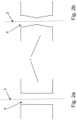
- Figure 1 shows a flow chart with several process steps for making an opening in a plate-shaped workpiece by irradiation with laser radiation and subsequent etching with individual process steps when making an opening in a plate-shaped workpiece 1.
- a laser beam 2 is directed onto the surface of the workpiece 1.
- the thickness d of the workpiece 1 is up to 3 mm.
- the exposure time of the laser beam 2 is chosen to be extremely short, so that only a modification of the workpiece 1 occurs concentrically around a beam axis of the laser beam.
- the laser is operated at a wavelength for which the workpiece 1 is transparent.
- Figure 1b represented in the form of a linear chain of bubbles.
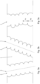
- the opening has a plurality of circumferential, concentric structures on the lateral surface, as shown in the illustrations of the Figures 2a and 2b as well as Figures 3a to 3c can be seen.
- the recess 4 is formed as a result of a successive etching of a plurality of defects 3 arranged in a row, in that the etching process successively connects the previously created defects 3, which are expanded by the etching effect to form a cavity in the workpiece 1.
- the etching fluid quickly moves from defect 3 to defect 3.
- the etching progresses from both above and below and begins simultaneously on both outer sides. Due to the relatively longer exposure time of the etching medium in the area of the outer sides, to a conical expansion of the defect 3 in the area of the outer surfaces as in the Figure 2b to recognize.
- Line 5 can be a straight line or follow a virtually arbitrary contour, which is precisely maintained by the etching process. This makes it possible for the first time to create virtually any cutting contour.
- the contour of the recess 4 or opening thus created is, after completion of the etching process, characterized by a sequence of cross-sectional widenings and constrictions, the shape of which is reminiscent of an earthworm, whereby the cross-sectional widenings and constrictions have neither a matching cross-sectional area, as for example in the Figures 2b and 3c to recognize, nor must they have a matching distance a1, a2, to adjacent cross-sectional extensions and constrictions, as shown in the Figure 3c
- a cross-sectional widening or constriction can be in a cross-sectional plane to the main axis or, as shown in the Figure 3a shown, arranged inclined thereto.
- Adjacent cross-sectional extensions or constrictions can also have centers that lie on a common line 5 that is inclined relative to the surface of the workpiece 1, so that the cross-sectional extensions or constrictions are arranged offset from one another, wherein the cross-sectional extensions or constrictions are arranged as shown in the Figure 3a shown inclined to the outer surface or as shown in the Figure 3b shown can be aligned parallel to the outer surface.
Landscapes
- Engineering & Computer Science (AREA)
- Physics & Mathematics (AREA)
- Optics & Photonics (AREA)
- Chemical & Material Sciences (AREA)
- Microelectronics & Electronic Packaging (AREA)
- Mechanical Engineering (AREA)
- Plasma & Fusion (AREA)
- Manufacturing & Machinery (AREA)
- Power Engineering (AREA)
- Condensed Matter Physics & Semiconductors (AREA)
- Computer Hardware Design (AREA)
- General Physics & Mathematics (AREA)
- Organic Chemistry (AREA)
- Life Sciences & Earth Sciences (AREA)
- Chemical Kinetics & Catalysis (AREA)
- General Chemical & Material Sciences (AREA)
- Geochemistry & Mineralogy (AREA)
- Materials Engineering (AREA)
- Inorganic Chemistry (AREA)
- Ceramic Engineering (AREA)
- Health & Medical Sciences (AREA)
- Toxicology (AREA)
- Laser Beam Processing (AREA)
- Surface Treatment Of Glass (AREA)
- Lead Frames For Integrated Circuits (AREA)
Priority Applications (1)
| Application Number | Priority Date | Filing Date | Title |
|---|---|---|---|
| EP22167179.5A EP4061101A1 (de) | 2014-09-16 | 2015-08-07 | Verfahren zum einbringen mindestens einer ausnehmung oder einer durchbrechung in ein plattenförmiges werkstück |
Applications Claiming Priority (3)
| Application Number | Priority Date | Filing Date | Title |
|---|---|---|---|
| DE102014113339.0A DE102014113339A1 (de) | 2014-09-16 | 2014-09-16 | Verfahren zur Erzeugung von Ausnehmungen in einem Material |
| DE102014116291 | 2014-11-07 | ||
| PCT/DE2015/100333 WO2016041544A1 (de) | 2014-09-16 | 2015-08-07 | Verfahren zum einbringen mindestens einer ausnehmung oder einer durchbrechung in ein plattenförmiges werkstück |
Related Child Applications (2)
| Application Number | Title | Priority Date | Filing Date |
|---|---|---|---|
| EP22167179.5A Division-Into EP4061101A1 (de) | 2014-09-16 | 2015-08-07 | Verfahren zum einbringen mindestens einer ausnehmung oder einer durchbrechung in ein plattenförmiges werkstück |
| EP22167179.5A Division EP4061101A1 (de) | 2014-09-16 | 2015-08-07 | Verfahren zum einbringen mindestens einer ausnehmung oder einer durchbrechung in ein plattenförmiges werkstück |
Publications (3)
| Publication Number | Publication Date |
|---|---|
| EP3195706A1 EP3195706A1 (de) | 2017-07-26 |
| EP3195706B1 EP3195706B1 (de) | 2022-06-01 |
| EP3195706B2 true EP3195706B2 (de) | 2025-05-14 |
Family
ID=54072638
Family Applications (2)
| Application Number | Title | Priority Date | Filing Date |
|---|---|---|---|
| EP15762474.3A Active EP3195706B2 (de) | 2014-09-16 | 2015-08-07 | Verfahren zum einbringen mindestens einer ausnehmung oder einer durchbrechung in ein plattenförmiges werkstück |
| EP22167179.5A Pending EP4061101A1 (de) | 2014-09-16 | 2015-08-07 | Verfahren zum einbringen mindestens einer ausnehmung oder einer durchbrechung in ein plattenförmiges werkstück |
Family Applications After (1)
| Application Number | Title | Priority Date | Filing Date |
|---|---|---|---|
| EP22167179.5A Pending EP4061101A1 (de) | 2014-09-16 | 2015-08-07 | Verfahren zum einbringen mindestens einer ausnehmung oder einer durchbrechung in ein plattenförmiges werkstück |
Country Status (11)
| Country | Link |
|---|---|
| US (2) | US11610784B2 (enExample) |
| EP (2) | EP3195706B2 (enExample) |
| JP (2) | JP6782692B2 (enExample) |
| KR (6) | KR102813417B1 (enExample) |
| CN (1) | CN107006128B (enExample) |
| ES (1) | ES2923764T5 (enExample) |
| LT (1) | LT3195706T (enExample) |
| MY (1) | MY196621A (enExample) |
| SG (2) | SG10201902331XA (enExample) |
| TW (1) | TWI616939B (enExample) |
| WO (1) | WO2016041544A1 (enExample) |
Families Citing this family (22)
| Publication number | Priority date | Publication date | Assignee | Title |
|---|---|---|---|---|
| DE102018100299A1 (de) * | 2017-01-27 | 2018-08-02 | Schott Ag | Strukturiertes plattenförmiges Glaselement und Verfahren zu dessen Herstellung |
| KR102356415B1 (ko) | 2017-03-06 | 2022-02-08 | 엘피케이에프 레이저 앤드 일렉트로닉스 악티엔게젤샤프트 | 전자기 방사선과 후속 에칭공정을 이용해 재료 안으로 적어도 하나의 리세스를 도입하기 위한 방법 |
| EP3592501B1 (de) | 2017-03-06 | 2021-10-06 | LPKF Laser & Electronics AG | Verfahren zur herstellung einer technischen maske |
| DE102018110211A1 (de) | 2018-04-27 | 2019-10-31 | Schott Ag | Verfahren zum Erzeugen feiner Strukturen im Volumen eines Substrates aus sprödharten Material |
| TWI678342B (zh) * | 2018-11-09 | 2019-12-01 | 財團法人工業技術研究院 | 形成導角的切割方法 |
| DE102020100848B4 (de) | 2019-01-29 | 2023-07-27 | Lpkf Laser & Electronics Aktiengesellschaft | Verfahren zur Mikrostrukturierung eines Glassubstrats mittels Laserstrahlung |
| DE102019201347B3 (de) * | 2019-02-01 | 2020-06-18 | Lpkf Laser & Electronics Ag | Herstellung von metallischen Leiterbahnen an Glas |
| KR20210124384A (ko) * | 2019-02-08 | 2021-10-14 | 코닝 인코포레이티드 | 펄스형 레이저 빔 초점 라인 및 증기 에칭을 사용하여 투명 워크피스를 레이저 가공하는 방법 |
| DE102019121827A1 (de) * | 2019-08-13 | 2021-02-18 | Trumpf Laser- Und Systemtechnik Gmbh | Laserätzen mit variierender Ätzselektivität |
| CN113594014B (zh) * | 2020-04-30 | 2024-04-12 | 中微半导体设备(上海)股份有限公司 | 零部件、等离子体反应装置及零部件加工方法 |
| DE102020114195A1 (de) | 2020-05-27 | 2021-12-02 | Lpkf Laser & Electronics Aktiengesellschaft | Verfahren zum Einbringen einer Ausnehmung in ein Substrat |
| DE102020118939A1 (de) * | 2020-07-17 | 2022-01-20 | Schott Ag | Glaswafer und Glaselement für Drucksensoren |
| CN111799169B (zh) * | 2020-07-17 | 2024-05-28 | 绍兴同芯成集成电路有限公司 | 一种飞秒激光结合hf湿蚀刻加工tgv的工艺 |
| DE102020120370B3 (de) | 2020-08-03 | 2022-02-03 | Infineon Technologies Ag | Mems-sensor mit partikelfilter und verfahren zu seiner herstellung |
| KR20220019158A (ko) | 2020-08-06 | 2022-02-16 | 삼성디스플레이 주식회사 | 윈도우 및 이를 포함하는 표시장치 |
| EP4011846A1 (en) | 2020-12-09 | 2022-06-15 | Schott Ag | Method of structuring a glass element and structured glass element produced thereby |
| DE102021204675B4 (de) | 2021-05-07 | 2023-05-17 | Lpkf Laser & Electronics Se | Vorrichtung und Verfahren zur Zellkultivierung |
| CN113510364B (zh) * | 2021-07-28 | 2022-11-25 | 广东工业大学 | 一种基于激光辅助溶解的三维空腔结构的成型方法 |
| EP4296244A1 (de) | 2022-06-21 | 2023-12-27 | LPKF Laser & Electronics SE | Substratträger aus glas zur bearbeitung eines substrats und ein verfahren zu dessen herstellung |
| DE102022127259A1 (de) | 2022-10-18 | 2024-04-18 | Lpkf Laser & Electronics Aktiengesellschaft | Verfahren sowie Vorrichtung zur Abbildung eines Strahls auf ein Objekt und Verfahren zum Einbringen einer Öffnung in ein Werkstück mittels dieses Verfahrens |
| DE102023125725A1 (de) * | 2023-09-22 | 2025-03-27 | Schott Ag | Laser-strukturiertes optisches Element |
| DE102024105120A1 (de) | 2024-02-23 | 2025-08-28 | Lpkf Laser & Electronics Se | Verfahren zur Integration und/oder Bearbeitung wenigstens eines Substrats sowie Substratstapel |
Citations (3)
| Publication number | Priority date | Publication date | Assignee | Title |
|---|---|---|---|---|
| US20140147624A1 (en) † | 2012-11-29 | 2014-05-29 | Corning Incorporated | Methods of Fabricating Glass Articles by Laser Damage and Etching |
| DE102013223637A1 (de) † | 2013-11-20 | 2015-05-21 | Trumpf Laser- Und Systemtechnik Gmbh | Verfahren zum Behandeln eines lasertransparenten Substrats zum anschließenden Trennen des Substrats |
| WO2015100056A1 (en) † | 2013-12-17 | 2015-07-02 | Corning Incorporated | Method for rapid laser drilling of holes in glass and products made therefrom |
Family Cites Families (17)
| Publication number | Priority date | Publication date | Assignee | Title |
|---|---|---|---|---|
| AU7091500A (en) * | 1999-08-30 | 2001-03-26 | Board Of Regents University Of Nebraska Lincoln | Three-dimensional electrical interconnects |
| JP4880820B2 (ja) | 2001-01-19 | 2012-02-22 | 株式会社レーザーシステム | レーザ支援加工方法 |
| JP4418282B2 (ja) | 2004-03-31 | 2010-02-17 | 株式会社レーザーシステム | レーザ加工方法 |
| JP4222296B2 (ja) | 2004-11-22 | 2009-02-12 | 住友電気工業株式会社 | レーザ加工方法とレーザ加工装置 |
| US9138913B2 (en) | 2005-09-08 | 2015-09-22 | Imra America, Inc. | Transparent material processing with an ultrashort pulse laser |
| JP2011218398A (ja) * | 2010-04-08 | 2011-11-04 | Fujikura Ltd | 微細構造の形成方法、レーザー照射装置、及び基板 |
| DE102010025966B4 (de) * | 2010-07-02 | 2012-03-08 | Schott Ag | Interposer und Verfahren zum Herstellen von Löchern in einem Interposer |
| KR102088722B1 (ko) * | 2010-07-12 | 2020-03-17 | 로핀-시나르 테크놀로지스 엘엘씨 | 레이저 필라멘테이션에 의한 재료 가공 방법 |
| WO2012014718A1 (ja) | 2010-07-26 | 2012-02-02 | 浜松ホトニクス株式会社 | インターポーザの製造方法 |
| KR101825238B1 (ko) * | 2010-07-26 | 2018-02-02 | 하마마츠 포토닉스 가부시키가이샤 | 광 흡수 기판의 제조 방법, 및 그것을 제조하기 위한 성형형의 제조 방법 |
| KR102035619B1 (ko) * | 2010-07-26 | 2019-12-16 | 하마마츠 포토닉스 가부시키가이샤 | 레이저 가공방법 |
| US8961806B2 (en) * | 2010-07-26 | 2015-02-24 | Hamamatsu Photonics K.K. | Laser processing method |
| US8933367B2 (en) | 2011-02-09 | 2015-01-13 | Sumitomo Electric Industries, Ltd. | Laser processing method |
| EP2754524B1 (de) | 2013-01-15 | 2015-11-25 | Corning Laser Technologies GmbH | Verfahren und Vorrichtung zum laserbasierten Bearbeiten von flächigen Substraten, d.h. Wafer oder Glaselement, unter Verwendung einer Laserstrahlbrennlinie |
| JP6113529B2 (ja) * | 2013-03-05 | 2017-04-12 | 株式会社ディスコ | ウエーハの加工方法 |
| EP3535221A1 (en) * | 2016-11-04 | 2019-09-11 | Corning Incorporated | Micro-perforated panel systems, applications, and methods of making micro-perforated panel systems |
| US11344973B2 (en) * | 2018-04-19 | 2022-05-31 | Corning Incorporated | Methods for forming holes in substrates |
-
2015
- 2015-08-07 EP EP15762474.3A patent/EP3195706B2/de active Active
- 2015-08-07 KR KR1020237018486A patent/KR102813417B1/ko active Active
- 2015-08-07 KR KR1020257016919A patent/KR102851778B1/ko active Active
- 2015-08-07 CN CN201580049903.1A patent/CN107006128B/zh active Active
- 2015-08-07 US US15/511,272 patent/US11610784B2/en active Active
- 2015-08-07 WO PCT/DE2015/100333 patent/WO2016041544A1/de not_active Ceased
- 2015-08-07 EP EP22167179.5A patent/EP4061101A1/de active Pending
- 2015-08-07 KR KR1020217005121A patent/KR20210022773A/ko not_active Ceased
- 2015-08-07 KR KR1020177007041A patent/KR20170044143A/ko not_active Ceased
- 2015-08-07 SG SG10201902331XA patent/SG10201902331XA/en unknown
- 2015-08-07 JP JP2017512917A patent/JP6782692B2/ja active Active
- 2015-08-07 KR KR1020257028228A patent/KR20250133802A/ko active Pending
- 2015-08-07 KR KR1020197015976A patent/KR20190065480A/ko not_active Ceased
- 2015-08-07 MY MYPI2017700845A patent/MY196621A/en unknown
- 2015-08-07 SG SG11201702091WA patent/SG11201702091WA/en unknown
- 2015-08-07 ES ES15762474T patent/ES2923764T5/es active Active
- 2015-08-07 LT LTEPPCT/DE2015/100333T patent/LT3195706T/lt unknown
- 2015-09-09 TW TW104129751A patent/TWI616939B/zh active
-
2020
- 2020-07-09 JP JP2020118488A patent/JP7049404B2/ja active Active
-
2022
- 2022-04-01 US US17/711,136 patent/US20220223434A1/en active Pending
Patent Citations (3)
| Publication number | Priority date | Publication date | Assignee | Title |
|---|---|---|---|---|
| US20140147624A1 (en) † | 2012-11-29 | 2014-05-29 | Corning Incorporated | Methods of Fabricating Glass Articles by Laser Damage and Etching |
| DE102013223637A1 (de) † | 2013-11-20 | 2015-05-21 | Trumpf Laser- Und Systemtechnik Gmbh | Verfahren zum Behandeln eines lasertransparenten Substrats zum anschließenden Trennen des Substrats |
| WO2015100056A1 (en) † | 2013-12-17 | 2015-07-02 | Corning Incorporated | Method for rapid laser drilling of holes in glass and products made therefrom |
Non-Patent Citations (2)
| Title |
|---|
| AMAKO JUN, ET AL: "Microstructuring transparent materials by use of nondiffracting ultrashort pulse beams generated by diffractive optics", J. OPT. SOC. AM., vol. 20, no. 12, 1 December 2003 (2003-12-01), pages 2562 - 2568, XP093033553 † |
| BUTKUS SIMAS, ET AL: "Rapid Cutting and Drilling of Transparent Materials via Femtosecond Laser Filamentation", JLMN JOURNAL OF LASER MICRO/NANOENGINEERING, vol. 9, no. 3, 29 July 2014 (2014-07-29), pages 213 - 220, XP093033533 † |
Also Published As
| Publication number | Publication date |
|---|---|
| KR20250079054A (ko) | 2025-06-04 |
| ES2923764T5 (en) | 2025-10-09 |
| EP3195706B1 (de) | 2022-06-01 |
| WO2016041544A1 (de) | 2016-03-24 |
| TWI616939B (zh) | 2018-03-01 |
| US20220223434A1 (en) | 2022-07-14 |
| KR102851778B1 (ko) | 2025-09-01 |
| US20170256422A1 (en) | 2017-09-07 |
| CN107006128B (zh) | 2020-05-19 |
| JP6782692B2 (ja) | 2020-11-11 |
| KR20190065480A (ko) | 2019-06-11 |
| ES2923764T3 (es) | 2022-09-30 |
| US11610784B2 (en) | 2023-03-21 |
| KR20170044143A (ko) | 2017-04-24 |
| EP3195706A1 (de) | 2017-07-26 |
| LT3195706T (lt) | 2022-08-10 |
| KR20250133802A (ko) | 2025-09-08 |
| CN107006128A (zh) | 2017-08-01 |
| SG11201702091WA (en) | 2017-04-27 |
| TW201621986A (zh) | 2016-06-16 |
| JP2020185613A (ja) | 2020-11-19 |
| EP4061101A1 (de) | 2022-09-21 |
| SG10201902331XA (en) | 2019-04-29 |
| KR20230084606A (ko) | 2023-06-13 |
| KR20210022773A (ko) | 2021-03-03 |
| KR102813417B1 (ko) | 2025-05-29 |
| JP7049404B2 (ja) | 2022-04-06 |
| MY196621A (en) | 2023-04-23 |
| JP2017534458A (ja) | 2017-11-24 |
Similar Documents
| Publication | Publication Date | Title |
|---|---|---|
| EP3195706B2 (de) | Verfahren zum einbringen mindestens einer ausnehmung oder einer durchbrechung in ein plattenförmiges werkstück | |
| EP2964417B1 (de) | Verfahren zum einbringen von durchbrechungen in ein substrat | |
| EP3592500B1 (de) | Verfahren zum einbringen zumindest einer ausnehmung in ein material mittels elektromagnetischer strahlung und anschliessendem ätzprozess | |
| EP2964416B1 (de) | Verfahren zum trennen eines substrates | |
| DE102014113339A1 (de) | Verfahren zur Erzeugung von Ausnehmungen in einem Material | |
| DE102013103370A1 (de) | Verfahren zum Einbringen von Durchbrechungen in ein Glassubstrat sowie ein derart hergestelltes Glassubstrat | |
| DE102018110211A1 (de) | Verfahren zum Erzeugen feiner Strukturen im Volumen eines Substrates aus sprödharten Material | |
| EP4013716B1 (de) | Verfahren zum bearbeiten eines werkstücks | |
| DE202012012732U1 (de) | Prägewalze aus Stahl mit einer strukturierten Oberfläche und Vorrichtung zum Erzeugen der strukturierten Oberfläche | |
| WO2017060252A1 (de) | Dielektrisches werkstück mit einer zone definiert ausgebildeter festigkeit sowie verfahren zu dessen herstellung und dessen verwendung | |
| WO2023012210A1 (de) | Verfahren und vorrichtung zur laserbearbeitung eines werkstücks | |
| DE102020114195A1 (de) | Verfahren zum Einbringen einer Ausnehmung in ein Substrat | |
| WO2021191218A1 (de) | Verfahren, system und werkstück, mit einem grossvolumigen entfernen von material des werkstückes durch laser-unterstütztes ätzen | |
| DE19535666A1 (de) | Verfahren zur Erzeugung einer Feinkeramikstruktur | |
| EP3875436B1 (de) | Verfahren zum vorbereiten und/oder durchführen des trennens eines substratelements und substratteilelement | |
| DE102017106372B4 (de) | Verfahren zur Bearbeitung eines Werkstückes | |
| DE102010032029B4 (de) | Verfahren zum Trennen einer runden Planplatte aus sprödbrüchigem Material in mehrere rechteckige Einzelplatten mittels Laser | |
| EP4514760A1 (de) | Verfahren zur trennung eines werkstücks | |
| WO2023041417A1 (de) | Verfahren und vorrichtung zur laserbearbeitung eines werkstücks | |
| WO2023088912A1 (de) | Verfahren zur laserbearbeitung eines werkstücks | |
| DE102021108505A1 (de) | Vorrichtung und Verfahren zur Laserbearbeitung eines Werkstücks | |
| DE102010013348A1 (de) | Technik zur Herstellung von Druckschablonen | |
| DE102024119224A1 (de) | Verfahren zum Bearbeiten eines Werkstücks aus sprödhartem Material | |
| DE102022122926A1 (de) | Transparentes Bauteil mit einer funktionalisierten Oberfläche |
Legal Events
| Date | Code | Title | Description |
|---|---|---|---|
| STAA | Information on the status of an ep patent application or granted ep patent |
Free format text: STATUS: THE INTERNATIONAL PUBLICATION HAS BEEN MADE |
|
| PUAI | Public reference made under article 153(3) epc to a published international application that has entered the european phase |
Free format text: ORIGINAL CODE: 0009012 |
|
| STAA | Information on the status of an ep patent application or granted ep patent |
Free format text: STATUS: REQUEST FOR EXAMINATION WAS MADE |
|
| 17P | Request for examination filed |
Effective date: 20170418 |
|
| AK | Designated contracting states |
Kind code of ref document: A1 Designated state(s): AL AT BE BG CH CY CZ DE DK EE ES FI FR GB GR HR HU IE IS IT LI LT LU LV MC MK MT NL NO PL PT RO RS SE SI SK SM TR |
|
| AX | Request for extension of the european patent |
Extension state: BA ME |
|
| DAV | Request for validation of the european patent (deleted) | ||
| DAX | Request for extension of the european patent (deleted) | ||
| STAA | Information on the status of an ep patent application or granted ep patent |
Free format text: STATUS: EXAMINATION IS IN PROGRESS |
|
| 17Q | First examination report despatched |
Effective date: 20190625 |
|
| GRAP | Despatch of communication of intention to grant a patent |
Free format text: ORIGINAL CODE: EPIDOSNIGR1 |
|
| STAA | Information on the status of an ep patent application or granted ep patent |
Free format text: STATUS: GRANT OF PATENT IS INTENDED |
|
| RIC1 | Information provided on ipc code assigned before grant |
Ipc: B23K 101/40 20060101ALN20220217BHEP Ipc: B23K 103/00 20060101ALN20220217BHEP Ipc: H01L 23/15 20060101ALN20220217BHEP Ipc: C03C 23/00 20060101ALI20220217BHEP Ipc: C03C 15/00 20060101ALI20220217BHEP Ipc: H01L 23/498 20060101ALI20220217BHEP Ipc: H01L 21/48 20060101ALI20220217BHEP Ipc: B23K 26/0622 20140101ALI20220217BHEP Ipc: B23K 26/382 20140101ALI20220217BHEP Ipc: H05K 3/00 20060101AFI20220217BHEP |
|
| INTG | Intention to grant announced |
Effective date: 20220318 |
|
| GRAS | Grant fee paid |
Free format text: ORIGINAL CODE: EPIDOSNIGR3 |
|
| GRAA | (expected) grant |
Free format text: ORIGINAL CODE: 0009210 |
|
| STAA | Information on the status of an ep patent application or granted ep patent |
Free format text: STATUS: THE PATENT HAS BEEN GRANTED |
|
| AK | Designated contracting states |
Kind code of ref document: B1 Designated state(s): AL AT BE BG CH CY CZ DE DK EE ES FI FR GB GR HR HU IE IS IT LI LT LU LV MC MK MT NL NO PL PT RO RS SE SI SK SM TR |
|
| REG | Reference to a national code |
Ref country code: GB Ref legal event code: FG4D Free format text: NOT ENGLISH |
|
| REG | Reference to a national code |
Ref country code: AT Ref legal event code: REF Ref document number: 1496291 Country of ref document: AT Kind code of ref document: T Effective date: 20220615 Ref country code: CH Ref legal event code: EP Ref country code: DE Ref legal event code: R096 Ref document number: 502015015879 Country of ref document: DE |
|
| REG | Reference to a national code |
Ref country code: IE Ref legal event code: FG4D Free format text: LANGUAGE OF EP DOCUMENT: GERMAN |
|
| REG | Reference to a national code |
Ref country code: CH Ref legal event code: PK Free format text: BERICHTIGUNGEN |
|
| RIN2 | Information on inventor provided after grant (corrected) |
Inventor name: OSTHOLT, ROMAN Inventor name: AMBROSIUS, NORBERT |
|
| REG | Reference to a national code |
Ref country code: NL Ref legal event code: FP |
|
| REG | Reference to a national code |
Ref country code: ES Ref legal event code: FG2A Ref document number: 2923764 Country of ref document: ES Kind code of ref document: T3 Effective date: 20220930 |
|
| PG25 | Lapsed in a contracting state [announced via postgrant information from national office to epo] |
Ref country code: SE Free format text: LAPSE BECAUSE OF FAILURE TO SUBMIT A TRANSLATION OF THE DESCRIPTION OR TO PAY THE FEE WITHIN THE PRESCRIBED TIME-LIMIT Effective date: 20220601 Ref country code: NO Free format text: LAPSE BECAUSE OF FAILURE TO SUBMIT A TRANSLATION OF THE DESCRIPTION OR TO PAY THE FEE WITHIN THE PRESCRIBED TIME-LIMIT Effective date: 20220901 Ref country code: HR Free format text: LAPSE BECAUSE OF FAILURE TO SUBMIT A TRANSLATION OF THE DESCRIPTION OR TO PAY THE FEE WITHIN THE PRESCRIBED TIME-LIMIT Effective date: 20220601 Ref country code: GR Free format text: LAPSE BECAUSE OF FAILURE TO SUBMIT A TRANSLATION OF THE DESCRIPTION OR TO PAY THE FEE WITHIN THE PRESCRIBED TIME-LIMIT Effective date: 20220902 Ref country code: FI Free format text: LAPSE BECAUSE OF FAILURE TO SUBMIT A TRANSLATION OF THE DESCRIPTION OR TO PAY THE FEE WITHIN THE PRESCRIBED TIME-LIMIT Effective date: 20220601 Ref country code: BG Free format text: LAPSE BECAUSE OF FAILURE TO SUBMIT A TRANSLATION OF THE DESCRIPTION OR TO PAY THE FEE WITHIN THE PRESCRIBED TIME-LIMIT Effective date: 20220901 |
|
| REG | Reference to a national code |
Ref country code: DE Ref legal event code: R083 Ref document number: 502015015879 Country of ref document: DE |
|
| PG25 | Lapsed in a contracting state [announced via postgrant information from national office to epo] |
Ref country code: RS Free format text: LAPSE BECAUSE OF FAILURE TO SUBMIT A TRANSLATION OF THE DESCRIPTION OR TO PAY THE FEE WITHIN THE PRESCRIBED TIME-LIMIT Effective date: 20220601 Ref country code: PL Free format text: LAPSE BECAUSE OF FAILURE TO SUBMIT A TRANSLATION OF THE DESCRIPTION OR TO PAY THE FEE WITHIN THE PRESCRIBED TIME-LIMIT Effective date: 20220601 Ref country code: LV Free format text: LAPSE BECAUSE OF FAILURE TO SUBMIT A TRANSLATION OF THE DESCRIPTION OR TO PAY THE FEE WITHIN THE PRESCRIBED TIME-LIMIT Effective date: 20220601 |
|
| PG25 | Lapsed in a contracting state [announced via postgrant information from national office to epo] |
Ref country code: SM Free format text: LAPSE BECAUSE OF FAILURE TO SUBMIT A TRANSLATION OF THE DESCRIPTION OR TO PAY THE FEE WITHIN THE PRESCRIBED TIME-LIMIT Effective date: 20220601 Ref country code: SK Free format text: LAPSE BECAUSE OF FAILURE TO SUBMIT A TRANSLATION OF THE DESCRIPTION OR TO PAY THE FEE WITHIN THE PRESCRIBED TIME-LIMIT Effective date: 20220601 Ref country code: RO Free format text: LAPSE BECAUSE OF FAILURE TO SUBMIT A TRANSLATION OF THE DESCRIPTION OR TO PAY THE FEE WITHIN THE PRESCRIBED TIME-LIMIT Effective date: 20220601 Ref country code: PT Free format text: LAPSE BECAUSE OF FAILURE TO SUBMIT A TRANSLATION OF THE DESCRIPTION OR TO PAY THE FEE WITHIN THE PRESCRIBED TIME-LIMIT Effective date: 20221003 Ref country code: EE Free format text: LAPSE BECAUSE OF FAILURE TO SUBMIT A TRANSLATION OF THE DESCRIPTION OR TO PAY THE FEE WITHIN THE PRESCRIBED TIME-LIMIT Effective date: 20220601 Ref country code: CZ Free format text: LAPSE BECAUSE OF FAILURE TO SUBMIT A TRANSLATION OF THE DESCRIPTION OR TO PAY THE FEE WITHIN THE PRESCRIBED TIME-LIMIT Effective date: 20220601 |
|
| PG25 | Lapsed in a contracting state [announced via postgrant information from national office to epo] |
Ref country code: IS Free format text: LAPSE BECAUSE OF FAILURE TO SUBMIT A TRANSLATION OF THE DESCRIPTION OR TO PAY THE FEE WITHIN THE PRESCRIBED TIME-LIMIT Effective date: 20221001 |
|
| REG | Reference to a national code |
Ref country code: DE Ref legal event code: R026 Ref document number: 502015015879 Country of ref document: DE |
|
| PLBI | Opposition filed |
Free format text: ORIGINAL CODE: 0009260 |
|
| PLAX | Notice of opposition and request to file observation + time limit sent |
Free format text: ORIGINAL CODE: EPIDOSNOBS2 |
|
| PG25 | Lapsed in a contracting state [announced via postgrant information from national office to epo] |
Ref country code: MC Free format text: LAPSE BECAUSE OF FAILURE TO SUBMIT A TRANSLATION OF THE DESCRIPTION OR TO PAY THE FEE WITHIN THE PRESCRIBED TIME-LIMIT Effective date: 20220601 Ref country code: AL Free format text: LAPSE BECAUSE OF FAILURE TO SUBMIT A TRANSLATION OF THE DESCRIPTION OR TO PAY THE FEE WITHIN THE PRESCRIBED TIME-LIMIT Effective date: 20220601 |
|
| 26 | Opposition filed |
Opponent name: GRUENECKER PATENT- UND RECHTSANWAELTE PARTG MBB Effective date: 20230301 |
|
| PG25 | Lapsed in a contracting state [announced via postgrant information from national office to epo] |
Ref country code: LU Free format text: LAPSE BECAUSE OF NON-PAYMENT OF DUE FEES Effective date: 20220807 Ref country code: DK Free format text: LAPSE BECAUSE OF FAILURE TO SUBMIT A TRANSLATION OF THE DESCRIPTION OR TO PAY THE FEE WITHIN THE PRESCRIBED TIME-LIMIT Effective date: 20220601 |
|
| PG25 | Lapsed in a contracting state [announced via postgrant information from national office to epo] |
Ref country code: SI Free format text: LAPSE BECAUSE OF FAILURE TO SUBMIT A TRANSLATION OF THE DESCRIPTION OR TO PAY THE FEE WITHIN THE PRESCRIBED TIME-LIMIT Effective date: 20220601 |
|
| PLBB | Reply of patent proprietor to notice(s) of opposition received |
Free format text: ORIGINAL CODE: EPIDOSNOBS3 |
|
| PG25 | Lapsed in a contracting state [announced via postgrant information from national office to epo] |
Ref country code: IE Free format text: LAPSE BECAUSE OF NON-PAYMENT OF DUE FEES Effective date: 20220807 |
|
| REG | Reference to a national code |
Ref country code: DE Ref legal event code: R082 Ref document number: 502015015879 Country of ref document: DE Representative=s name: CREUTZBURG, TOM, DIPL.-ING., DE |
|
| PG25 | Lapsed in a contracting state [announced via postgrant information from national office to epo] |
Ref country code: HU Free format text: LAPSE BECAUSE OF FAILURE TO SUBMIT A TRANSLATION OF THE DESCRIPTION OR TO PAY THE FEE WITHIN THE PRESCRIBED TIME-LIMIT; INVALID AB INITIO Effective date: 20150807 |
|
| PG25 | Lapsed in a contracting state [announced via postgrant information from national office to epo] |
Ref country code: CY Free format text: LAPSE BECAUSE OF FAILURE TO SUBMIT A TRANSLATION OF THE DESCRIPTION OR TO PAY THE FEE WITHIN THE PRESCRIBED TIME-LIMIT Effective date: 20220601 |
|
| PG25 | Lapsed in a contracting state [announced via postgrant information from national office to epo] |
Ref country code: MK Free format text: LAPSE BECAUSE OF FAILURE TO SUBMIT A TRANSLATION OF THE DESCRIPTION OR TO PAY THE FEE WITHIN THE PRESCRIBED TIME-LIMIT Effective date: 20220601 |
|
| PLAB | Opposition data, opponent's data or that of the opponent's representative modified |
Free format text: ORIGINAL CODE: 0009299OPPO |
|
| R26 | Opposition filed (corrected) |
Opponent name: GRUENECKER PATENT- UND RECHTSANWAELTE PARTG MBB Effective date: 20230301 |
|
| RAP4 | Party data changed (patent owner data changed or rights of a patent transferred) |
Owner name: LPKF LASER & ELECTRONICS SE |
|
| PG25 | Lapsed in a contracting state [announced via postgrant information from national office to epo] |
Ref country code: MT Free format text: LAPSE BECAUSE OF FAILURE TO SUBMIT A TRANSLATION OF THE DESCRIPTION OR TO PAY THE FEE WITHIN THE PRESCRIBED TIME-LIMIT Effective date: 20220601 |
|
| PG25 | Lapsed in a contracting state [announced via postgrant information from national office to epo] |
Ref country code: BG Free format text: LAPSE BECAUSE OF FAILURE TO SUBMIT A TRANSLATION OF THE DESCRIPTION OR TO PAY THE FEE WITHIN THE PRESCRIBED TIME-LIMIT Effective date: 20220601 |
|
| PG25 | Lapsed in a contracting state [announced via postgrant information from national office to epo] |
Ref country code: BG Free format text: LAPSE BECAUSE OF FAILURE TO SUBMIT A TRANSLATION OF THE DESCRIPTION OR TO PAY THE FEE WITHIN THE PRESCRIBED TIME-LIMIT Effective date: 20220601 |
|
| PUAH | Patent maintained in amended form |
Free format text: ORIGINAL CODE: 0009272 |
|
| STAA | Information on the status of an ep patent application or granted ep patent |
Free format text: STATUS: PATENT MAINTAINED AS AMENDED |
|
| 27A | Patent maintained in amended form |
Effective date: 20250514 |
|
| AK | Designated contracting states |
Kind code of ref document: B2 Designated state(s): AL AT BE BG CH CY CZ DE DK EE ES FI FR GB GR HR HU IE IS IT LI LT LU LV MC MK MT NL NO PL PT RO RS SE SI SK SM TR |
|
| REG | Reference to a national code |
Ref country code: DE Ref legal event code: R102 Ref document number: 502015015879 Country of ref document: DE |
|
| REG | Reference to a national code |
Ref country code: NL Ref legal event code: FP |
|
| PGFP | Annual fee paid to national office [announced via postgrant information from national office to epo] |
Ref country code: NL Payment date: 20250821 Year of fee payment: 11 |
|
| REG | Reference to a national code |
Ref country code: CH Ref legal event code: R18 Free format text: ST27 STATUS EVENT CODE: U-0-0-R10-R18 (AS PROVIDED BY THE NATIONAL OFFICE) Effective date: 20251008 |
|
| PGFP | Annual fee paid to national office [announced via postgrant information from national office to epo] |
Ref country code: ES Payment date: 20250917 Year of fee payment: 11 |
|
| REG | Reference to a national code |
Ref country code: ES Ref legal event code: DC2A Ref document number: 2923764 Country of ref document: ES Kind code of ref document: T5 Effective date: 20251009 |
|
| PGFP | Annual fee paid to national office [announced via postgrant information from national office to epo] |
Ref country code: LT Payment date: 20250728 Year of fee payment: 11 Ref country code: DE Payment date: 20250831 Year of fee payment: 11 |
|
| PGFP | Annual fee paid to national office [announced via postgrant information from national office to epo] |
Ref country code: IT Payment date: 20250829 Year of fee payment: 11 |
|
| PGFP | Annual fee paid to national office [announced via postgrant information from national office to epo] |
Ref country code: BE Payment date: 20250820 Year of fee payment: 11 Ref country code: GB Payment date: 20250822 Year of fee payment: 11 |
|
| PGFP | Annual fee paid to national office [announced via postgrant information from national office to epo] |
Ref country code: AT Payment date: 20250819 Year of fee payment: 11 Ref country code: FR Payment date: 20250827 Year of fee payment: 11 |
|
| PGFP | Annual fee paid to national office [announced via postgrant information from national office to epo] |
Ref country code: CH Payment date: 20250901 Year of fee payment: 11 |
|
| REG | Reference to a national code |
Ref country code: NL Ref legal event code: PD Owner name: LPKF LASER & ELECTRONICS SE; DE Free format text: DETAILS ASSIGNMENT: CHANGE OF OWNER(S), CHANGE OF LEGAL ENTITY; FORMER OWNER NAME: LPKF LASER & ELECTRONICS AG Effective date: 20251110 |