EP3190488A1 - Verkabelungskörper, leiterplatte, berührungssensor und verfahren zur herstellung eines verkabelungskörpers - Google Patents
Verkabelungskörper, leiterplatte, berührungssensor und verfahren zur herstellung eines verkabelungskörpers Download PDFInfo
- Publication number
- EP3190488A1 EP3190488A1 EP15873291.7A EP15873291A EP3190488A1 EP 3190488 A1 EP3190488 A1 EP 3190488A1 EP 15873291 A EP15873291 A EP 15873291A EP 3190488 A1 EP3190488 A1 EP 3190488A1
- Authority
- EP
- European Patent Office
- Prior art keywords
- conductor pattern
- wiring body
- wiring
- side portion
- electrically conductive
- Prior art date
- Legal status (The legal status is an assumption and is not a legal conclusion. Google has not performed a legal analysis and makes no representation as to the accuracy of the status listed.)
- Granted
Links
Images


Classifications
-
- G—PHYSICS
- G06—COMPUTING; CALCULATING OR COUNTING
- G06F—ELECTRIC DIGITAL DATA PROCESSING
- G06F3/00—Input arrangements for transferring data to be processed into a form capable of being handled by the computer; Output arrangements for transferring data from processing unit to output unit, e.g. interface arrangements
- G06F3/01—Input arrangements or combined input and output arrangements for interaction between user and computer
- G06F3/03—Arrangements for converting the position or the displacement of a member into a coded form
- G06F3/041—Digitisers, e.g. for touch screens or touch pads, characterised by the transducing means
-
- H—ELECTRICITY
- H05—ELECTRIC TECHNIQUES NOT OTHERWISE PROVIDED FOR
- H05K—PRINTED CIRCUITS; CASINGS OR CONSTRUCTIONAL DETAILS OF ELECTRIC APPARATUS; MANUFACTURE OF ASSEMBLAGES OF ELECTRICAL COMPONENTS
- H05K3/00—Apparatus or processes for manufacturing printed circuits
- H05K3/10—Apparatus or processes for manufacturing printed circuits in which conductive material is applied to the insulating support in such a manner as to form the desired conductive pattern
- H05K3/20—Apparatus or processes for manufacturing printed circuits in which conductive material is applied to the insulating support in such a manner as to form the desired conductive pattern by affixing prefabricated conductor pattern
- H05K3/207—Apparatus or processes for manufacturing printed circuits in which conductive material is applied to the insulating support in such a manner as to form the desired conductive pattern by affixing prefabricated conductor pattern using a prefabricated paste pattern, ink pattern or powder pattern
-
- H—ELECTRICITY
- H05—ELECTRIC TECHNIQUES NOT OTHERWISE PROVIDED FOR
- H05K—PRINTED CIRCUITS; CASINGS OR CONSTRUCTIONAL DETAILS OF ELECTRIC APPARATUS; MANUFACTURE OF ASSEMBLAGES OF ELECTRICAL COMPONENTS
- H05K3/00—Apparatus or processes for manufacturing printed circuits
- H05K3/38—Improvement of the adhesion between the insulating substrate and the metal
- H05K3/386—Improvement of the adhesion between the insulating substrate and the metal by the use of an organic polymeric bonding layer, e.g. adhesive
-
- G—PHYSICS
- G06—COMPUTING; CALCULATING OR COUNTING
- G06F—ELECTRIC DIGITAL DATA PROCESSING
- G06F2203/00—Indexing scheme relating to G06F3/00 - G06F3/048
- G06F2203/041—Indexing scheme relating to G06F3/041 - G06F3/045
- G06F2203/04103—Manufacturing, i.e. details related to manufacturing processes specially suited for touch sensitive devices
-
- G—PHYSICS
- G06—COMPUTING; CALCULATING OR COUNTING
- G06F—ELECTRIC DIGITAL DATA PROCESSING
- G06F3/00—Input arrangements for transferring data to be processed into a form capable of being handled by the computer; Output arrangements for transferring data from processing unit to output unit, e.g. interface arrangements
- G06F3/01—Input arrangements or combined input and output arrangements for interaction between user and computer
- G06F3/03—Arrangements for converting the position or the displacement of a member into a coded form
- G06F3/041—Digitisers, e.g. for touch screens or touch pads, characterised by the transducing means
- G06F3/044—Digitisers, e.g. for touch screens or touch pads, characterised by the transducing means by capacitive means
-
- H—ELECTRICITY
- H05—ELECTRIC TECHNIQUES NOT OTHERWISE PROVIDED FOR
- H05K—PRINTED CIRCUITS; CASINGS OR CONSTRUCTIONAL DETAILS OF ELECTRIC APPARATUS; MANUFACTURE OF ASSEMBLAGES OF ELECTRICAL COMPONENTS
- H05K1/00—Printed circuits
- H05K1/02—Details
- H05K1/0274—Optical details, e.g. printed circuits comprising integral optical means
-
- H—ELECTRICITY
- H05—ELECTRIC TECHNIQUES NOT OTHERWISE PROVIDED FOR
- H05K—PRINTED CIRCUITS; CASINGS OR CONSTRUCTIONAL DETAILS OF ELECTRIC APPARATUS; MANUFACTURE OF ASSEMBLAGES OF ELECTRICAL COMPONENTS
- H05K1/00—Printed circuits
- H05K1/02—Details
- H05K1/09—Use of materials for the conductive, e.g. metallic pattern
- H05K1/092—Dispersed materials, e.g. conductive pastes or inks
-
- H—ELECTRICITY
- H05—ELECTRIC TECHNIQUES NOT OTHERWISE PROVIDED FOR
- H05K—PRINTED CIRCUITS; CASINGS OR CONSTRUCTIONAL DETAILS OF ELECTRIC APPARATUS; MANUFACTURE OF ASSEMBLAGES OF ELECTRICAL COMPONENTS
- H05K2201/00—Indexing scheme relating to printed circuits covered by H05K1/00
- H05K2201/01—Dielectrics
- H05K2201/0104—Properties and characteristics in general
- H05K2201/0108—Transparent
-
- H—ELECTRICITY
- H05—ELECTRIC TECHNIQUES NOT OTHERWISE PROVIDED FOR
- H05K—PRINTED CIRCUITS; CASINGS OR CONSTRUCTIONAL DETAILS OF ELECTRIC APPARATUS; MANUFACTURE OF ASSEMBLAGES OF ELECTRICAL COMPONENTS
- H05K2201/00—Indexing scheme relating to printed circuits covered by H05K1/00
- H05K2201/09—Shape and layout
- H05K2201/09209—Shape and layout details of conductors
- H05K2201/09654—Shape and layout details of conductors covering at least two types of conductors provided for in H05K2201/09218 - H05K2201/095
- H05K2201/09681—Mesh conductors, e.g. as a ground plane
-
- H—ELECTRICITY
- H05—ELECTRIC TECHNIQUES NOT OTHERWISE PROVIDED FOR
- H05K—PRINTED CIRCUITS; CASINGS OR CONSTRUCTIONAL DETAILS OF ELECTRIC APPARATUS; MANUFACTURE OF ASSEMBLAGES OF ELECTRICAL COMPONENTS
- H05K2201/00—Indexing scheme relating to printed circuits covered by H05K1/00
- H05K2201/09—Shape and layout
- H05K2201/09818—Shape or layout details not covered by a single group of H05K2201/09009 - H05K2201/09809
- H05K2201/09827—Tapered, e.g. tapered hole, via or groove
-
- H—ELECTRICITY
- H05—ELECTRIC TECHNIQUES NOT OTHERWISE PROVIDED FOR
- H05K—PRINTED CIRCUITS; CASINGS OR CONSTRUCTIONAL DETAILS OF ELECTRIC APPARATUS; MANUFACTURE OF ASSEMBLAGES OF ELECTRICAL COMPONENTS
- H05K2203/00—Indexing scheme relating to apparatus or processes for manufacturing printed circuits covered by H05K3/00
- H05K2203/01—Tools for processing; Objects used during processing
- H05K2203/0104—Tools for processing; Objects used during processing for patterning or coating
- H05K2203/0113—Female die used for patterning or transferring, e.g. temporary substrate having recessed pattern
-
- H—ELECTRICITY
- H05—ELECTRIC TECHNIQUES NOT OTHERWISE PROVIDED FOR
- H05K—PRINTED CIRCUITS; CASINGS OR CONSTRUCTIONAL DETAILS OF ELECTRIC APPARATUS; MANUFACTURE OF ASSEMBLAGES OF ELECTRICAL COMPONENTS
- H05K2203/00—Indexing scheme relating to apparatus or processes for manufacturing printed circuits covered by H05K3/00
- H05K2203/05—Patterning and lithography; Masks; Details of resist
- H05K2203/0502—Patterning and lithography
-
- H—ELECTRICITY
- H05—ELECTRIC TECHNIQUES NOT OTHERWISE PROVIDED FOR
- H05K—PRINTED CIRCUITS; CASINGS OR CONSTRUCTIONAL DETAILS OF ELECTRIC APPARATUS; MANUFACTURE OF ASSEMBLAGES OF ELECTRICAL COMPONENTS
- H05K3/00—Apparatus or processes for manufacturing printed circuits
- H05K3/10—Apparatus or processes for manufacturing printed circuits in which conductive material is applied to the insulating support in such a manner as to form the desired conductive pattern
- H05K3/12—Apparatus or processes for manufacturing printed circuits in which conductive material is applied to the insulating support in such a manner as to form the desired conductive pattern using thick film techniques, e.g. printing techniques to apply the conductive material or similar techniques for applying conductive paste or ink patterns
- H05K3/1275—Apparatus or processes for manufacturing printed circuits in which conductive material is applied to the insulating support in such a manner as to form the desired conductive pattern using thick film techniques, e.g. printing techniques to apply the conductive material or similar techniques for applying conductive paste or ink patterns by other printing techniques, e.g. letterpress printing, intaglio printing, lithographic printing, offset printing
Definitions
- the present invention relates to a wiring body, a wiring board, a touch sensor, and a method for producing the wiring body.
- an electromagnetic shielding material there is known one having a conductive layer formed by pressing a printing plate having a depression of a predetermined pattern filled with an uncured conductive composition and one surface of a substrate to which the conductive composition is transferred through an uncured primer layer, transferring the conductive composition onto the primer layer, and performing hardening treatment on the conductive composition (for example, see paragraph [0087] of Patent Document 2).
- the conductor wiring pattern or the conductive layer of the electromagnetic shielding material described above is formed by performing hardening/heating treatment after transferring the conductor material (conductive composition), and thus a concave-convex shape originating from conductive particles included in the conductor material is generated on a surface of the conductor wiring pattern. For this reason, there is a problem that light entering from the outside is diffused on the surface of the conductor wiring pattern. Meanwhile, even when surface roughness of the whole conductor wiring pattern is reduced to suppress diffused reflection, there is a problem that there is difficulty in strongly bonding the conductor material and the substrate together.
- Problems to be solved by the present invention include providing a wiring body, a wiring board, a touch sensor, and a method for producing the wiring body capable of suppressing diffused reflection of light entering from the outside while stringing bonding an insulating member and a conductor pattern together.
- a surface roughness of an adhesive surface of a conductor pattern bonded to an insulating member is rougher than a surface roughness of another surface except for the adhesive surface in the conductor pattern, it is possible to suppress diffused reflection of light entering from the outside while strongly bonding an insulating member and a conductor pattern together.
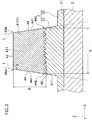
- Fig. 1 is a perspective view illustrating a wiring board in an embodiment
- Fig. 2 is a cross-sectional view taken along II-II line of Fig. 1
- Fig. 3 is a cross-sectional view taken along III-III line of Fig. 1
- Figs. 4(A) to 4(C) are cross-sectional views illustrating first to third modified examples of a wiring body in the embodiment of the invention.
- the wiring board 10 (wiring body 1) in the present embodiment is used as an electrode substrate, etc. of a touch sensor of a touch panel, etc.
- a touch sensor is used as an input device having a function of detecting a touch position by combining the wiring board 10 (wiring body 1) and a display device (not illustrated) together.
- the display device is not particularly restricted, and a liquid crystal display, an organic EL display, electronic paper, etc. may be used as the display device.
- a touch sensor corresponding to a projection-type capacitive sensing method using two wiring boards 10 (wiring bodies 1), etc. is present as the touch sensor.
- one of the two wiring boards 10 disposed to face each other is used as a detection electrode, the other one is used as a driving electrode, and a predetermined voltage is periodically applied to between the two electrodes from an external circuit (not illustrated).
- a capacitor capacitor
- the touch sensor may detect an operation position of the operator based on an electrical change between the two electrodes.
- the wiring board 10 includes the wiring body 1 and a substrate 2 supporting the wiring body 1.
- the wiring body 1 includes an adhesive layer 3 serving as an insulating member and a conductive layer 4.
- Use of the wiring board 10 (wiring body 1) is not particularly restricted to the above-described use.
- the conductive layer 4 has a mesh shape (net shape) including straight line-shaped conductor patterns 41.
- a shape of each net formed by the conductor patterns 41 corresponds to a substantially square shape.
- the shape of each net may correspond to the geometric forms below. That is, the shape of the net may correspond to a triangle such as a regular triangle, an isosceles triangle, a right triangle, etc., and may correspond to a rectangle such as a parallelogram, a trapezoid, etc.
- the shape of the net may correspond to an n-polygon such as a hexagon, an octagon, a dodecagon, an icosagon, etc., a circle, an ellipse, a star, etc.
- the conductor pattern 41 corresponds to a straight line shape.
- the conductor pattern 41 is not particularly restricted thereto when the conductor pattern 41 linearly extends.
- the conductor pattern 41 may correspond to a curved shape, a horseshoe shape, a zigzag line shape, etc.
- a planar shape of the conductive layer 4 is not particularly restricted thereto.
- the planar shape may correspond to a straight line rather than the mesh shape, and the conductor pattern 41 may correspond to a curved shape.
- the conductor pattern 41 may have a non-uniform width in planar view.
- the substrate 2 is a transparent substrate that may transmit visible light and supports the wiring body 1.
- a material included in the substrate 2 may include polyethylene terephthalate (PET), polyethylene naphthalate (PEN), polyimide resin (PI), polyetherimide resin (PEI), polycarbonate (PC), polyether ether ketone (PEEK), liquid crystal polymer (LCP), cycloolefin polymer (COP), silicone resin (SI), acrylic resin, phenol resin, epoxy resin, green sheet, glass, etc.
- An easily adhesive layer or an optical adjustment layer may be formed in the substrate 2.
- the adhesive layer 3 serving as the insulating member is a layer for holding the conductor pattern 41 on the substrate 2, and is made of, for example, an insulating material such as a UV-curing resin, a thermosetting resin, a thermoplastic resin, ceramic green sheet, etc. such as epoxy resin, acrylic resin, polyester resin, urethane resin, vinyl resin, silicone resin, phenol resin, polyimide resin, etc.
- the adhesive layer 3 includes a support portion 31 supporting the conductor pattern 41 and a smooth portion 32 covering a main surface 21 of the substrate 2 except for a part of the main surface 21 that is covered with the support portion 31, and the support portion 31 and the smooth portion 32 are integrally formed.
- a thickness of the smooth portion 32 may be set within a range of 5 ⁇ m to 100 ⁇ m.
- a cross-sectional shape (cross-sectional shape with respect to an extending direction of the conductor pattern 41) of the support portion 31 in the present embodiment corresponds to a shape, a width of which narrows in a direction away from the substrate 2 (+Z direction of Fig. 2 ).
- a boundary between the support portion 31 and the conductor pattern 41 has a concave-convex shape corresponding to a concave-convex shape of a lower surface (adhesive surface) 42 of the conductor pattern 41.
- a concave-convex shape is formed based on a surface roughness of the adhesive surface 42 of the conductor pattern 41.
- a boundary between the support portion 31 and the conductor pattern 41 in a cross section along the extending direction of the conductor pattern 41 has a concave-convex shape corresponding to the concave-convex shape of the adhesive surface 42 of the conductor pattern 41.
- Surface roughness of the adhesive surface 42 will be described below in detail.
- the concave-convex shape of the boundary between the support portion 31 and the conductor pattern 41 is exaggeratingly illustrated to describe the wiring body 1 of the present embodiment in an easily understood manner.
- the smooth portion 32 is provided on the whole main surface 21 of the substrate 2 at a substantially uniform height (thickness).
- the height of the smooth portion 32 is relatively lower than a height of the support portion 31. For this reason, the support portion 31 protrudes with respect to the smooth portion 32, and rigidity of the wiring body 1 is improved in the support portion 31.
- the smooth portion 32 may be formed only on a portion of the main surface 21 of the substrate 2 except for the support portion 31.
- the height of the smooth portion 32 may be equal to the height of the support portion 31.
- the height of the smooth portion 32 may be larger than the height of the support portion 31.
- the smooth portion 32 may be omitted from the adhesive layer 3, and the adhesive layer 3 may only include the support portion 31. In this case, optical transparency of the whole wiring body 1 is improved, and thus it is possible to improve visibility in the touch panel, etc. mounted with the wiring body 1.
- the adhesive layer 3 in the present embodiment corresponds to an example of an insulating member of the invention.
- the conductive layer 4 (conductor pattern 41) is a layer that functions as an electrode in the touch sensor or a lead-out wire electrically connected to the electrode.
- the conductive layer 4 is formed by applying and hardening conductive paste.
- Specific examples of the conductive paste included in the conductive layer 4 may include conductive paste configured by mixing conductive powder or metal salt with binder resin, water, or a solvent and various addition agents.
- Examples of the conductive powder may include metal such as silver, copper, nickel, tin, bismuth, zinc, indium, palladium, etc., or a carbon-based material such as graphite, carbon black (furnace black, acetylene black, Ketjen black), carbon nanotube, carbon nanofiber, etc.
- Examples of the metal salt may include salt of the above-mentioned metal.
- conductive particles having a diameter of 0.5 ⁇ m or more and 2 ⁇ m or less (0.5 ⁇ (j) ⁇ 2) depending on the width of the formed conductor pattern 41 may be used as the conductive particles contained in the conductive layer 4 (conductor pattern 41). It is preferable to use conductive particles having an average diameter ⁇ of less than or equal to half the width of the formed conductor pattern 41 in terms of stabilizing electrical resistivity in the conductor pattern 41.
- the carbon-based material is used as the conductive powder, it is preferable to use a particle whose specific surface area measured by a BET method is 20 m 2 /g or more.
- a metal material is preferably used as conductive powder.
- a carbon-based material may be used as conductive powder. Using a carbon-based material as conductive particles is preferable in terms of improving haze or total light reflectance of a mesh film.
- binder resin contained in the conductive paste may include acrylic resin, polyester resin, epoxy resin, vinyl resin, urethane resin, phenol resin, polyimide resin, silicone resin, fluoride resin, etc.
- solvent contained in the conductive paste may include ⁇ -terpineol, butyl carbitol acetate, butyl carbitol, 1-decanol, butyl cellosolve, diethylene glycol monoethyl ether acetate, tetradecane, etc.
- the binder resin may be omitted from the material contained in the conductive layer 4.
- the width of the conductor pattern 41 is preferably within a range of 50 nm to 1,000 ⁇ m, more preferably within a range of 500 nm to 150 ⁇ m, even more preferably within a range of 1 ⁇ m to 10 ⁇ m, and further even more preferably within a range of 1 ⁇ m to 5 ⁇ m.
- the height of the conductor pattern 41 is preferably within a range of 50 nm to 3,000 ⁇ m, more preferably within a range of 500 nm to 450 ⁇ m, and even more preferably within a range of 500 nm to 10 ⁇ m.
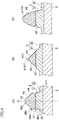
- the conductor pattern 41 of the present embodiment includes the adhesive surface 42, a top portion 43, and two side portions 44 and 44.
- the top portion 43 is positioned on an opposite side from the adhesive surface 42 in the conductor pattern 41.
- the top portion 43 is substantially parallel to the main surface 21 of the substrate 2 (an upper surface of the smooth portion 32 of the adhesive layer 3).
- the top portion 43 includes a flat portion 431 in a cross section of the conductor pattern 41 in a width direction.
- the flat portion 431 is a portion having a straight line shape (that is, a portion having an extremely large radius of curvature) in the cross section of the conductor pattern 41 in the width direction, and has a flatness of 0.5 ⁇ m or less.
- the flatness may be measured by the JIS method (JIS B0621 (1984)).
- the flatness of the flat portion 431 is obtained using a non-contact measurement scheme using laser light.
- a measuring object for example, the top portion 43 or the side portion 44
- an image of reflected light thereof is formed on an image pick-up device (for example, a two-dimensional (2D) CMOS) to measure the flatness.
- a scheme maximum deflection-type flatness
- a scheme of measuring or calculating the flatness is not particularly restricted to the above-described schemes.
- a scheme of measuring the flatness may correspond to a contact-type measurement scheme using a dial gauge, etc.
- a scheme maximum tilt-type flatness
- a scheme may be used as a scheme of calculating the flatness to calculate a value of a gap, which is generated when a target plane is interposed between parallel planes, as the flatness.
- the flat portion 431 of the present embodiment is formed substantially in the whole of the top portion 43.
- the flat portion may be formed in a portion of the top portion without being particularly restricted to the above description. In this case, for example, the flat portion may be formed in a region not including both ends of the top portion 43.
- a width of the flat portion 431 is at least half or more a width of the top portion 43.
- the side portion 44 is positioned between the adhesive surface 42 and the top portion 43.
- the side portion 44 has a first portion 44a connected to the top portion 43 and a second portion 44b connected to the adhesive surface 42.
- the second potion 44b is positioned on an outside of the first portion 44a.
- a virtual straight line L (indicated by an alternated long and short dash line in Fig. 2 ) is a straight line passing through the first and second portions 44a and 44b in the cross section of the conductor pattern 41 in the width direction.
- the virtual straight line L is inclined to approach a center in the cross section of the conductor pattern 41 in the width direction as being separated from the adhesive layer 3.
- the side portion 44 of the present embodiment extends to substantially match the virtual straight line L. That is, the side portion 44 is inclined such that the side portion 44 approaches the center in a cross-sectional shape of the conductor pattern 41 as the side portion is away from the adhesive layer 3. Inclined angles of the two side portions 44 and 44 in one conductor pattern 41 are substantially equal to each other.
- the side portion 44 includes a flat portion 441 in the cross section of the conductor pattern 41 in the width direction.
- the flat portion 441 is a portion having a straight line shape (that is, a portion having an extremely large radius of curvature) in the cross section of the conductor pattern 41 in the width direction, and has a flatness of 0.5 ⁇ m or less.
- a portion of the side portion 44 substantially matching the virtual straight line L is included in the flat portion 441. That is, the flat portion 441 is formed substantially in the whole of the side portion 44.
- a shape of the side portion 44 is not particularly restricted to the above-described shape.
- the side portion 44 may extrude outward from the virtual straight line L in the cross section of the conductor pattern 41 in the width direction. That is, the side portion 44 preferably has a shape which is not recessed inward from the virtual straight line L (a shape in which a hem of the conductor pattern does not widen) in the cross section of the conductor pattern 41 in the width direction.
- the flat portion 441 is formed in the whole side portion 44.
- the invention is not particularly restricted thereto, and the flat portion 441 may be formed in a portion of the side portion 44.
- the side portion 44 of the conductor pattern 41 and a side portion 311 of the support portion 31 in the adhesive layer 3 are smoothly connected to each other to form one plane.
- the side portion 311 of the support portion 31 preferably has a shape in which a hem of the support portion 31 does not widen in the cross section of the conductor pattern 41 in the width direction.
- the cross-sectional shape of the conductor pattern 41 included in the conductive layer 4 is substantially a trapezoidal shape as illustrated in Fig. 2 .
- the invention is not particularly restricted thereto.
- the cross-sectional shape of the conductor pattern 41 may correspond to a square shape, a rectangular shape, etc.
- the cross-sectional shape of the conductor pattern 41 may include the top portion 43 and the side portion 44, and a second side portion 45 formed between the top portion 43 and the side portion 44.
- the second side portion 45 is formed to be inclined toward a central line C more than the side portion 44 in the cross-sectional shape of the conductor pattern 41.
- the second side portion 45 extends to substantially match a virtual straight line L2 passing through a third portion 45a at which the second side portion 45 and the top portion 43 are connected to each other and a fourth portion 45b at which the side portion 44 and the second side portion 45 are connected to each other.
- the first portion 44a of the side portion 44 is substantially identical to the fourth portion 45b of the second side portion 45.
- the second side portion 45 preferably has a shape which is not recessed inward from the virtual straight line L2 (a shape in which the hem of the conductor pattern does not widen) in the cross section of the conductor pattern 41 in the width direction.
- the cross-sectional shape of the conductor pattern 41 may not have the top portion 43, and right and left side portions 44 may be connected to each other at a vertex 441.
- a surface except for the lower surface (adhesive surface) 42 in the conductor pattern 41 may include a curved surface 46 formed in a convex shape in a direction away from the substrate 2.
- the cross-sectional shape of the conductor pattern 41 has a bilaterally symmetric shape.
- the cross-sectional shape may correspond to a bilaterally asymmetric shape.
- the side portion 44 of the conductor pattern 41 is inclined at a predetermined angle with respect to the adhesive surface 42 (average surface).
- the top portion 43 of the conductor pattern 41 is substantially parallel to the main surface 21 of the substrate 2(the upper surface of the smooth portion 32 of the adhesive layer 3) as described above.
- an angle ⁇ between the side portion 44 and the top portion 43 is preferably within a range of 90° to 170° (90° ⁇ 170°), more preferably within a range of 90° to 120° (90° ⁇ 120°) in terms of suppressing diffused reflection of light in the side portion 44.
- an angle between one side portion 44 and the top portion 43 is substantially identical to an angle between the other side portion 44 and the top portion 43.
- the top portion 43 includes the flat portion 431 (smooth surface), and the surface roughness of the adhesive surface 42 is rougher than a surface roughness of the top portion 43 including the flat portion 431.
- the surface roughness Ra of the adhesive surface 42 of the conductor pattern 41 is within a range of about 0.1 ⁇ m to 3 ⁇ m
- the surface roughness Ra of the top portion 43 is within a range of about 0.001 ⁇ m to 1.0 ⁇ m.
- a ratio of the surface roughness of the top portion 43 to the surface roughness of the adhesive surface 42 is greater than or equal to 0.01 and less than 1.
- the surface roughness Ra of the adhesive surface 42 is preferably within a range of 0.1 to 0.5 ⁇ m, and the surface roughness Ra of the top portion 43 is preferably within a range of 0.001 ⁇ m to 0.3 ⁇ m.
- the surface roughness of the top portion 43 is preferably one fifth or less of the width (maximum width A) of the conductor pattern 41.
- the ratio of the surface roughness of the top portion 43 to the surface roughness of the adhesive surface 42 is preferably greater than or equal to 0.1 and less than 1.
- Such a surface roughness may be measured by the JIS method (JIS B0601 (revised on March 21, 2013).
- the surface roughness of the adhesive surface 42 and the surface roughness of the top portion 43 may be measured along a width direction in the conductor pattern 41 (see Fig. 2 ).
- the roughness may be measured along an extending direction in the conductor pattern 41 (see Fig. 3 ).
- the "surface roughness Ra” herein refers to an “arithmetic average roughness Ra”.
- This "arithmetic average roughness Ra” refers to a roughness parameter obtained by excluding a long wavelength component (waviness component) from a profile curve. The waviness component is separated from the profile curve based on a measurement condition (for example, dimensions of an object, etc.) necessary to obtain a form.
- the side portion 44 includes the flat portion 441.
- the surface roughness of the adhesive surface 42 is rougher than the surface roughness of the side portion 44 including the flat portion 441.
- the surface roughness Ra of the side portion 44 is within a range of about 0.001 ⁇ m to 1.0 ⁇ m with respect to the surface roughness Ra of the adhesive surface 42.
- the surface roughness Ra of the side portion 44 is preferably within a range of about 0.001 ⁇ m to 0.3 ⁇ m.
- the surface roughness of the side portion 44 may be measured along the width direction in the conductor pattern 41 (see Fig. 2 ), or may be measured along the extending direction in the conductor pattern 41 (see Fig. 3 ).
- a diffused reflectance of the wiring body 1 on a surface side except for the adhesive surface 42 is relatively smaller than a diffused reflectance of the wiring body 1 on the adhesive surface 42 side.
- a ratio of the diffused reflectance of the wiring body 1 on the surface side except for the adhesive surface 42 to the diffused reflectance of the wiring body 1 on the adhesive surface 42 side is greater than or equal to 0.1 and less than 1, and preferably greater than or equal to 0.3 and less than 1.
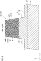
- FIG. 5 A description will be given of an example of a shape of a conductor pattern 41B having the above-described relative relation between an adhesive surface and another surface with reference to Fig. 5 .
- a conductor pattern 41B containing conductive particles M and a binder resin B
- conductive particles M is dispersed in the binder resin B.
- some of the conductive particles M protrude from the binder resin B on an adhesive surface 42B.
- the adhesive surface 42B has a concave-convex shape.
- the binder resin B penetrates between conductive particles M and covers the conductive particles M in a top portion 43B and a side portion 44B. In this way, a flat portion 431B is formed in the top portion 43B. In addition, a flat portion 441B is formed in the side portion 44B.
- a surface roughness of the adhesive surface 42B is relatively large due to some of the conductive particles M protruding from the binder resin B on the adhesive surface 42B. Meanwhile, in the top portion 43B, a surface roughness of the top portion 43B is relatively small due to the conductive particles M covered with the binder resin B. In this way, the surface roughness of the adhesive surface 42B is rougher than the surface roughness of the top portion 43B.
- a surface roughness of the side portion 44B is relatively small due to the conductive particles M covered with the binder resin B.
- the surface roughness of the adhesive surface 42B is rougher than the surface roughness of the side portion 44B.
- Shapes of the adhesive surface, the top portion, and the side portion are not restricted to the mode illustrated in Fig. 5 when the above-described relative relation with regard to the surface roughness is satisfied.
- Fig. 6(A) to Fig. 6(E) are cross-sectional views for description of the method for producing the wiring board in the present embodiment.
- intaglio 5 in which a recessed portion 51 having a shape corresponding to the mesh shape of the conductive layer 4 is prepared.
- a material contained in the intaglio 5 may include glass of nickel, silicon, silicon dioxide, etc., ceramic, organic silica, glassy carbon, a thermoplastic resin, a light curing resin, etc.
- a width of the recessed portion 51 is preferably within a range of 50 nm to 1,000 nm, more preferably within a range of 500 nm to 150 ⁇ m, even more preferably within a range of 1 ⁇ m to 10 ⁇ m, and further even more preferably within a range of 1 ⁇ m to 5 ⁇ m.
- a height of the recessed portion 51 is preferably within a range of 50 nm to 3,000 ⁇ m, more preferably within a range of 500 nm to 450 ⁇ m, and even more preferably within a range of 500 nm to 10 ⁇ m.
- An inner wall 52 of the recessed portion 51 in the present embodiment corresponds to a flat surface, and the inner wall 52 is inclined such that a width thereof is narrowed toward a bottom surface 53 of the recessed portion 51 (see a drawn diagram of Fig. 6(A) ).
- a release layer made of a graphite-based material, a silicone-based material, a fluorine-based material, a ceramic-based material, an aluminum-based material, etc. is preferably formed on a surface of the intaglio 5 including the recessed portion 51 in order to improve a release property.
- the recessed portion 51 of the intaglio 5 is filled with an electrically conductive material 6 (first process).
- the above-described conductive paste is used as the electrically conductive material 6.
- it is possible to use a material to which conductivity is assigned through heating. Examples of a method of filling the recessed portion 51 of the intaglio 5 with the electrically conductive material 6 may include a dispensing method, an ink-jet method, screen printing, etc.
- the examples may include a method in which after coating using a slit coating method, a bar coating method, a blade coating method, a dip coating method, a spray coating method, or a spin coating method, an electrically conductive material coated in a portion other than the recessed portion is removed by wiping, scraping, sucking, sticking, washing, or blowing.
- a composition, etc. of the electrically conductive material may be appropriately used properly according to a shape of the intaglio, etc.
- the conductor pattern 41 included in the conductive layer 4 is formed by heating the electrically conductive material 6 filling the recessed portion 51 of the intaglio 5.
- a condition for heating the electrically conductive material 6 may be appropriately set depending on the composition of the electrically conductive material 6, etc.
- the electrically conductive material 6 contracts in volume through this heating process.
- an external surface of the electrically conductive material 6 except for an upper surface 47 is formed in a shape having a flat surface along the inner wall 52 and the bottom surface 53 of the recessed portion 51.
- the upper surface 47 of the electrically conductive material 6 filling the recessed portion 51 is heated while coming into contact with an external atmosphere. For this reason, a concave-convex shape based on the shape of the conductive particles contained in the electrically conductive material 6 is formed on the upper surface 47 of the conductor pattern 41 (second process).
- the electrically conductive material 6 is heated and hardened in the present process, and thus wet spreading does not occur even when the electrically conductive material 6 is taken out from the recessed portion 51 of the intaglio 5 in a subsequent process.
- a method of processing the electrically conductive material is not restricted to heating.
- the electrically conductive material may be irradiated with an energy ray such as an infrared ray, an ultraviolet ray, laser light, or may only be dried. Alternatively, two or more types of these processing methods may be combined.
- an adhesive material 7 for forming the adhesive layer 3 is disposed on the intaglio 5.
- the above-described material contained in the adhesive layer 3 is used as the adhesive material 7.
- Examples of a method of disposing the adhesive material 7 on the intaglio 5 include screen printing, a spray coating method, a bar coating method, a dip method, an ink-jet method, etc.
- the adhesive material 7 introduces into the recessed portion 51 including a concave of the concave-convex shape of the conductor pattern 41 (third process).
- the substrate 2 is disposed from above the adhesive material 7 applied onto the intaglio 5. This disposition is preferably performed in a vacuum in order to inhibit a bubble from penetrating between the adhesive material 7 and the substrate 2.
- a material of the substrate may include the above-described materials.
- An easily adhesive layer or an optical adjustment layer may be formed in the substrate.
- the adhesive material 7 is hardened. Examples of a method of hardening the adhesive material may include irradiating with an energy ray such as an infrared ray, an ultraviolet ray, laser light, etc., heating, annealing, drying, etc. In this way, the adhesive layer 3 is formed, and the substrate 2 and the conductor pattern 41 are bonded and fixed to each other through the adhesive layer 3.
- the substrate 2 is stacked after the adhesive material 7 is disposed onto the intaglio 5.
- the invention is not particularly restricted thereto.
- the substrate 2 may be stacked on the intaglio 5 through the adhesive material 7 by disposing, on the intaglio 5, a layer obtained by applying the adhesive material 7 to the main surface (surface facing the intaglio 5) of the substrate 2 in advance.
- the substrate 2, the adhesive layer 3, and the conductive layer 4 may be released from a mold (fourth process), thereby obtaining the wiring board 10 (wiring body 1) (see Fig. 6(E) ).
- the wiring body illustrated in Fig. 4(A) to 4(C) may be produced similarly to the above description using intaglio that has recessed portions corresponding to the shapes of the conductor pattern 41 and the support portion 31.
- Fig. 7 is a cross-sectional view for description of the effect of the wiring body in the present embodiment.
- a focus is on relative relation between surface roughness (that is, a roughness parameter obtained by excluding a wavelength component) of the adhesive surface 42 in the conductor pattern 41 and surface roughness of another surface which is a surface of the conductor pattern 41 except for the adhesive surface 42 (the surface including the top portion 43 and the side portion 44), and the surface roughness Ra of the adhesive surface 42 is set to be relatively rougher than the surface roughness Ra of the other surface. For this reason, it is possible to suppress diffused reflection of light entering from the outside while strongly bonding the adhesive layer 3 and the conductor pattern 41 together.
- the width of the conductor pattern 41 is within a range of 1 ⁇ m to 5 ⁇ m, and when the relative relation between the surface roughness of the adhesive surface 42 and the surface roughness of the other surface satisfies the above-described relation, it is possible to noticeably accomplish the effect that diffused reflection of light entering from the outside may be suppressed while strongly bonding the adhesive layer 3 and the conductor pattern 41 together.
- the electrically conductive material 6 is heated after filling the recessed portion 51 of the intaglio 5 with the electrically conductive material 6 as described above.
- the bottom surface of the electrically conductive material 6 after heating has a flat portion corresponding to the flat surface of the bottom surface 53 of the recessed portion 51.
- the top portion 43 of the conductor pattern 41 included in the conductive layer 4 has the flat portion 431.
- the wiring body 1 is used as an electrode substrate of a touch panel, etc., it is possible to further suppress diffused reflection of light entering from the outside of the wiring body 1. As a result, it is possible to improve visibility of the touch panel, etc. mounted with the wiring body 1.
- a side surface of the electrically conductive material 6 after heating includes a flat portion corresponding to a flat surface of the inner wall 52 of the recessed portion 51.
- the side portion 44 of the conductor pattern 41 included in the conductive layer 4 includes the flat portion 441.
- a bubble is rarely formed around a surface of the conductor pattern 41 when the top portion 43 of the conductor pattern 41 includes the flat portion 431. In this way, it is possible to inhibit light entering from the outside of the wiring body 1 from diffusing on the bubble when the wiring body 1 is used as the electrode substrate, etc. of the touch panel. For this reason, it is possible to further improve visibility of the touch panel, etc. mounted with the wiring body 1.
- a bubble is rarely formed around the surface of the conductor pattern 41, it is possible to inhibit the conductor pattern 41 from being corroded by water present inside the bubble.
- the side portion 44 of the conductor pattern 41 includes the flat portion 441
- a bubble is rarely formed around the surface of the conductor pattern 41.
- a bubble is rarely formed around the surface of the conductor pattern 41, it is possible to inhibit the conductor pattern 41 from being corroded by water present inside the bubble.
- the top portion 43 includes the flat portion 431 in the cross-sectional shape of the conductor pattern 41 in the width direction, an external surface 81 of the coat layer 8 is easily formed in a flat shape. In this way, when a film (not illustrated) is provided on the external surface 81 of the coat layer 8, it is possible to suppress generation of distortion in the film while stably holding the film by the external surface 81 of the coat layer 8.
- the side portion 44 extends to substantially match the virtual straight line L passing through the first and second portions 44a and 44b.
- the side portion does not have a shape recessed inward from the virtual straight line (a shape in which a hem of the conductor pattern widens) in the cross section of the conductor pattern in the width direction, diffused reflection of light entering form the outside of the wiring body 1 is suppressed. It is possible to further improve visibility of the touch panel, etc. by mounting the wiring body 1 in the touch panel, etc.
- a diffused reflectance of the wiring body 1 on the other surface side is relatively smaller than a diffused reflectance of the wiring body 1 on the adhesive surface 42 side.
- the diffused reflectance of the wiring body 1 is small, it is possible to inhibit the conductor pattern 41 from appearing white, and to suppress a decrease in contract in a region in which the conductor pattern 41 may be visually recognized. In this way, it is possible to further improve visibility of the touch panel, etc. mounted with the wiring body 1 of the present embodiment.
- a concave-convex shape based on the shape of the conductive particles contained in the electrically conductive material 6 is formed on the upper surface 47 of the electrically conductive material 6 after heating. That is, the concave-convex shape is formed on the lower surface (adhesive surface) 42 of the conductor pattern 41 included in the conductive layer 4. It is possible to increase a contact area between the conductor pattern 41 and the adhesive layer 3, and to strongly bond the conductor pattern 41 and the adhesive layer 3 together by the concave-convex shape. Meanwhile, a contact surface between the conductor pattern 41 and the intaglio 5 has a flat shape.
- the inner wall 52 of the recessed portion 51 of the intaglio 5 is inclined with respect to the upper surface 47 (the adhesive surface 42) of the electrically conductive material 6 (the conductive layer 4), and the width of the recessed portion 51 is narrowed toward the bottom surface 53, and thus this effect may be further improved.
- Inclining the inner wall 52 of the recessed portion 51 as described above contributes to improving a filling property when the inner wall 52 is filled with the electrically conductive material 6 (see Fig. 4(A) ).
- the conductor pattern 41 and the adhesive layer 3 may be strongly bonded together, the conductor pattern 41 may be inhibited from being peeled off from the adhesive layer 3 by the wiring body 1 being curved or bent, and thus durability of the wiring body 1 may be improved.
- the cross-sectional shape of the electrically conductive material 6 (the conductor pattern 41) after heating may be set to a shape satisfying the above Formula (3) and Formula (4) by the effect that the release property is improved when the conductor pattern 41 is released from the intaglio 5. In this way, it is possible to increase a cross-sectional area of the conductor pattern 41, and to decrease an electrical resistance value per unit length of the conductor pattern 41. This effect is further improved when the inequalities B/A ⁇ 3 and D/C ⁇ 3 are satisfied.
- a wiring body 1B may be produced using a producing method illustrated in Fig. 8(A) to Fig. 8(E) . Specifically, after the intaglio 5 is filled with the electrically conductive material 6 and heated ( Fig. 8(A) and Fig. 8(B) ), an adhesive material 7B is disposed on the intaglio 5 ( Fig. 8(C) ), and the adhesive material 7B is hardened ( Fig. 8(D) ). Then, the wiring body 1B having the hardened adhesive material 7B (the adhesive body 71) used as a substrate may be produced by releasing the electrically conductive material 6 (the conductor pattern 41) and an adhesive body 71 after heating from the intaglio 5. The wiring body 1B produced in this way may accomplish a similar effect to that of the above-described wiring body 1.
- the touch sensor of the above embodiment is a touch sensor corresponding to a projection-type capacitive sensing method using two wiring boards 10 (wiring bodies 1).
- the invention is not restricted thereto.
- the invention is applicable to a touch sensor corresponding to a surface-type (capacitive coupling-type) capacitive sensing method using one wiring board (wiring body).
- a metal material mixed with a carbon-based material may be used as the conductive powder of the conductive layer 4 (conductor pattern).
- the carbon-based material may be disposed on the top portion side of the conductor pattern, and the metal-based material may be disposed on the adhesive surface side thereof.
- the metal-based material may be disposed on the top portion side of the conductor pattern, and the carbon-based material may be disposed on the adhesive surface side thereof.
- the substrate 2 may be omitted from the wiring body 1 in the above-described embodiment.
- the wiring body may be configured in a mode in which a release sheet is provided on a lower surface of the adhesive layer 3, and the wiring body is mounted by peeling off the release sheet and bonding the wiring body to a mounting object (a film, surface glass, a polarizing plate, display glass, etc.) at the time of amounting.
- a mounting object a film, surface glass, a polarizing plate, display glass, etc.
- the mounting object on which the wiring body is mounted corresponds to an example of a support of the invention.
- the wiring body may be used as a heater by electrifying the wiring body to generate heat using resistance heating, etc.
- a carbon-based material having relatively high electrical resistivity is preferably used as conductive powder of the conductive layer (conductor pattern).
- the wiring body may be used as an electromagnetic shield by grounding a part of a conductive portion of the wiring body.
- the wiring body may be used as an antenna.
- a mounting object on which the wiring body is mounted corresponds to an example of the support of the invention.
Applications Claiming Priority (2)
| Application Number | Priority Date | Filing Date | Title |
|---|---|---|---|
| JP2014264492 | 2014-12-26 | ||
| PCT/JP2015/086271 WO2016104723A1 (ja) | 2014-12-26 | 2015-12-25 | 配線体、配線基板、タッチセンサ、及び配線体の製造方法 |
Publications (3)
| Publication Number | Publication Date |
|---|---|
| EP3190488A1 true EP3190488A1 (de) | 2017-07-12 |
| EP3190488A4 EP3190488A4 (de) | 2017-10-25 |
| EP3190488B1 EP3190488B1 (de) | 2019-05-15 |
Family
ID=56150735
Family Applications (1)
| Application Number | Title | Priority Date | Filing Date |
|---|---|---|---|
| EP15873291.7A Not-in-force EP3190488B1 (de) | 2014-12-26 | 2015-12-25 | Verkabelungskörper, leiterplatte, berührungssensor und verfahren zur herstellung eines verkabelungskörpers |
Country Status (6)
| Country | Link |
|---|---|
| US (1) | US10379645B2 (de) |
| EP (1) | EP3190488B1 (de) |
| JP (2) | JP6046867B2 (de) |
| CN (1) | CN106687893B (de) |
| TW (1) | TWI587191B (de) |
| WO (1) | WO2016104723A1 (de) |
Families Citing this family (11)
| Publication number | Priority date | Publication date | Assignee | Title |
|---|---|---|---|---|
| CN106605455B (zh) * | 2015-01-30 | 2020-04-14 | 株式会社藤仓 | 布线体、布线基板以及触摸传感器 |
| CN104820533B (zh) * | 2015-05-22 | 2019-03-12 | 京东方科技集团股份有限公司 | 触摸基板及其制备方法、显示装置 |
| CN107124900A (zh) * | 2015-12-25 | 2017-09-01 | 松下知识产权经营株式会社 | 触摸面板和使用该触摸面板的显示装置 |
| EP3487268A4 (de) * | 2016-07-12 | 2020-03-11 | Fujikura, Ltd. | Dehnbares substrat |
| GB201613051D0 (en) | 2016-07-28 | 2016-09-14 | Landa Labs (2012) Ltd | Applying an electrical conductor to a substrate |
| JP2019046405A (ja) * | 2017-09-07 | 2019-03-22 | 日本航空電子工業株式会社 | タッチセンサデバイス |
| KR102083184B1 (ko) * | 2018-04-17 | 2020-03-02 | 울산과학기술원 | 자가 부착 투명 전극 및 이의 제조방법 |
| EP3859887A4 (de) * | 2018-09-28 | 2022-07-27 | Dai Nippon Printing Co., Ltd. | Leiterplatte und verfahren zur herstellung der leiterplatte |
| JP7115687B2 (ja) * | 2019-01-23 | 2022-08-09 | 株式会社デンソー | カーボンナノチューブパターン配線、それを有する透明導電基板およびヒータ |
| KR20210000805A (ko) * | 2019-06-25 | 2021-01-06 | 삼성디스플레이 주식회사 | 표시 장치의 제조 방법 및 이에 사용되는 레이저 장치 |
| CN115428259A (zh) * | 2020-05-01 | 2022-12-02 | 大日本印刷株式会社 | 配线基板和配线基板的制造方法 |
Family Cites Families (25)
| Publication number | Priority date | Publication date | Assignee | Title |
|---|---|---|---|---|
| JPH04240792A (ja) * | 1991-01-24 | 1992-08-28 | Matsushita Electric Ind Co Ltd | 回路基板の製造方法 |
| US5201268A (en) | 1990-12-25 | 1993-04-13 | Matsushita Electric Industrial Co., Ltd. | Intaglio printing process and its application |
| US5609704A (en) | 1993-09-21 | 1997-03-11 | Matsushita Electric Industrial Co., Ltd. | Method for fabricating an electronic part by intaglio printing |
| JP3039285B2 (ja) * | 1993-09-21 | 2000-05-08 | 松下電器産業株式会社 | 電子部品およびその製造方法 |
| DE112005000179T5 (de) * | 2004-01-13 | 2006-11-30 | Dai Nippon Printing Co., Ltd. | Abschirmfolie für elektromagnetische Wellen und Verfahren zur Herstellung dieser |
| US8033016B2 (en) | 2005-04-15 | 2011-10-11 | Panasonic Corporation | Method for manufacturing an electrode and electrode component mounted body |
| JP4617978B2 (ja) * | 2005-04-15 | 2011-01-26 | パナソニック株式会社 | 配線基板の製造方法 |
| EP1720389B1 (de) | 2005-04-25 | 2019-07-03 | Brother Kogyo Kabushiki Kaisha | Verfahren zur Herstellung eines Musters |
| TW200738913A (en) | 2006-03-10 | 2007-10-16 | Mitsui Mining & Smelting Co | Surface treated elctrolytic copper foil and process for producing the same |
| JP2007324426A (ja) * | 2006-06-02 | 2007-12-13 | Hitachi Ltd | パターン形成方法、導体配線パターン |
| KR100782412B1 (ko) | 2006-10-25 | 2007-12-05 | 삼성전기주식회사 | 전사회로 형성방법 및 회로기판 제조방법 |
| JP5096735B2 (ja) | 2006-12-05 | 2012-12-12 | Jx日鉱日石エネルギー株式会社 | ワイヤグリッド型偏光子及びその製造方法、並びにそれを用いた位相差フィルム及び液晶表示素子 |
| CN101557927B (zh) * | 2006-12-27 | 2014-10-22 | 日立化成株式会社 | 凹版和使用该凹版的带有导体层图形的基材 |
| WO2008149969A1 (ja) | 2007-06-08 | 2008-12-11 | Dai Nippon Printing Co., Ltd. | 印刷物及びその製造方法並びに電磁波シールド材及びその製造方法 |
| WO2010064630A1 (ja) * | 2008-12-02 | 2010-06-10 | 大日本印刷株式会社 | 電磁波シールド材、及びその製造方法 |
| TWI467214B (zh) * | 2009-09-02 | 2015-01-01 | Dexerials Corp | A conductive optical element, a touch panel, an information input device, a display device, a solar cell, and a conductive optical element |
| JP5404468B2 (ja) | 2010-02-22 | 2014-01-29 | 京セラ株式会社 | 回路基板 |
| JP2012033466A (ja) * | 2010-07-02 | 2012-02-16 | Fujifilm Corp | 導電層転写材料、及びタッチパネル |
| JP2012155369A (ja) | 2011-01-21 | 2012-08-16 | Japan Aviation Electronics Industry Ltd | 静電容量式タッチパネル |
| JP2012168301A (ja) | 2011-02-14 | 2012-09-06 | Bridgestone Corp | 金属細線の形成方法及びこれを用いたワイヤグリッド型偏光子の製造方法 |
| CN103384870B (zh) | 2011-02-18 | 2016-06-01 | 富士胶片株式会社 | 导电片和触控面板 |
| JP6019662B2 (ja) * | 2012-03-28 | 2016-11-02 | 大日本印刷株式会社 | 透視性電極部材、及び画像表示装置 |
| JP2014021401A (ja) * | 2012-07-20 | 2014-02-03 | Dexerials Corp | 導電性光学素子、入力素子、および表示素子 |
| JP5922008B2 (ja) | 2012-11-30 | 2016-05-24 | 富士フイルム株式会社 | 転写フィルムおよび透明積層体、それらの製造方法、静電容量型入力装置ならびに画像表示装置 |
| JP5704200B2 (ja) | 2013-08-21 | 2015-04-22 | 大日本印刷株式会社 | タッチパネル用電極フィルム及びタッチパネル |
-
2015
- 2015-12-25 TW TW104143738A patent/TWI587191B/zh not_active IP Right Cessation
- 2015-12-25 EP EP15873291.7A patent/EP3190488B1/de not_active Not-in-force
- 2015-12-25 US US15/508,310 patent/US10379645B2/en active Active
- 2015-12-25 WO PCT/JP2015/086271 patent/WO2016104723A1/ja active Application Filing
- 2015-12-25 CN CN201580047455.1A patent/CN106687893B/zh not_active Expired - Fee Related
- 2015-12-25 JP JP2016532147A patent/JP6046867B2/ja active Active
-
2016
- 2016-11-17 JP JP2016223848A patent/JP6735212B2/ja not_active Expired - Fee Related
Also Published As
| Publication number | Publication date |
|---|---|
| US10379645B2 (en) | 2019-08-13 |
| JP6735212B2 (ja) | 2020-08-05 |
| CN106687893B (zh) | 2020-05-22 |
| JP2017041654A (ja) | 2017-02-23 |
| TW201636797A (zh) | 2016-10-16 |
| TWI587191B (zh) | 2017-06-11 |
| US20170285786A1 (en) | 2017-10-05 |
| WO2016104723A1 (ja) | 2016-06-30 |
| EP3190488A4 (de) | 2017-10-25 |
| EP3190488B1 (de) | 2019-05-15 |
| JP6046867B2 (ja) | 2016-12-21 |
| CN106687893A (zh) | 2017-05-17 |
| JPWO2016104723A1 (ja) | 2017-04-27 |
Similar Documents
| Publication | Publication Date | Title |
|---|---|---|
| EP3190488B1 (de) | Verkabelungskörper, leiterplatte, berührungssensor und verfahren zur herstellung eines verkabelungskörpers | |
| US10101865B2 (en) | Wiring body, wiring board, and touch sensor | |
| US9983448B2 (en) | Wiring body assembly, structure with conductor layer, and touch sensor | |
| EP3396500A1 (de) | Schaltungskörper, schaltungssubstrat und berührungssensor | |
| US10345936B2 (en) | Method for producing conductor-layer-provided structure, substrate-provided wiring body, substrate-provided structure, and touch sensor | |
| EP3197250A1 (de) | Schaltungskörper, schaltungssubstrat und berührungssensor | |
| TWI629619B (zh) | Touching the wiring harness for the detector, touching the wiring board for the detector, and touching the detector | |
| EP3451132A1 (de) | Verdrahtungskörper, verdrahtungskörperanordnung, verdrahtungssubstrat und berührungssensor | |
| US9910552B2 (en) | Wiring body, wiring board, touch sensor, and method for producing wiring body | |
| JP6483801B2 (ja) | タッチセンサ | |
| EP3438799A1 (de) | Verdrahtungskörper, verdrahtungssubstrat, berührungssensor und verfahren zur herstellung des verdrahtungskörpers | |
| US20180307344A1 (en) | Wiring body, wiring board, touch sensor, and manufacturing method of wiring body | |
| US20190073065A1 (en) | Wiring body, wiring board, and touch sensor | |
| EP3438800A1 (de) | Verdrahtungskörper, leiterplatte und berührungssensor |
Legal Events
| Date | Code | Title | Description |
|---|---|---|---|
| STAA | Information on the status of an ep patent application or granted ep patent |
Free format text: STATUS: THE INTERNATIONAL PUBLICATION HAS BEEN MADE |
|
| PUAI | Public reference made under article 153(3) epc to a published international application that has entered the european phase |
Free format text: ORIGINAL CODE: 0009012 |
|
| STAA | Information on the status of an ep patent application or granted ep patent |
Free format text: STATUS: REQUEST FOR EXAMINATION WAS MADE |
|
| 17P | Request for examination filed |
Effective date: 20170227 |
|
| AK | Designated contracting states |
Kind code of ref document: A1 Designated state(s): AL AT BE BG CH CY CZ DE DK EE ES FI FR GB GR HR HU IE IS IT LI LT LU LV MC MK MT NL NO PL PT RO RS SE SI SK SM TR |
|
| AX | Request for extension of the european patent |
Extension state: BA ME |
|
| RIC1 | Information provided on ipc code assigned before grant |
Ipc: H05K 3/38 20060101ALI20170914BHEP Ipc: H05K 1/09 20060101ALN20170914BHEP Ipc: H05K 1/02 20060101ALN20170914BHEP Ipc: H05K 3/12 20060101ALN20170914BHEP Ipc: G06F 3/041 20060101AFI20170914BHEP Ipc: H05K 3/20 20060101ALI20170914BHEP |
|
| A4 | Supplementary search report drawn up and despatched |
Effective date: 20170922 |
|
| DAV | Request for validation of the european patent (deleted) | ||
| DAX | Request for extension of the european patent (deleted) | ||
| REG | Reference to a national code |
Ref country code: DE Ref legal event code: R079 Ref document number: 602015030562 Country of ref document: DE Free format text: PREVIOUS MAIN CLASS: G06F0003041000 Ipc: H05K0003200000 |
|
| GRAP | Despatch of communication of intention to grant a patent |
Free format text: ORIGINAL CODE: EPIDOSNIGR1 |
|
| STAA | Information on the status of an ep patent application or granted ep patent |
Free format text: STATUS: GRANT OF PATENT IS INTENDED |
|
| RIC1 | Information provided on ipc code assigned before grant |
Ipc: H05K 3/12 20060101ALN20181025BHEP Ipc: H05K 1/09 20060101ALN20181025BHEP Ipc: H05K 3/20 20060101AFI20181025BHEP Ipc: H05K 3/38 20060101ALI20181025BHEP Ipc: H05K 1/02 20060101ALN20181025BHEP Ipc: G06F 3/041 20060101ALI20181025BHEP |
|
| RIC1 | Information provided on ipc code assigned before grant |
Ipc: H05K 3/38 20060101ALI20181114BHEP Ipc: H05K 1/09 20060101ALN20181114BHEP Ipc: H05K 3/20 20060101AFI20181114BHEP Ipc: H05K 3/12 20060101ALN20181114BHEP Ipc: G06F 3/041 20060101ALI20181114BHEP Ipc: H05K 1/02 20060101ALN20181114BHEP |
|
| INTG | Intention to grant announced |
Effective date: 20181128 |
|
| GRAS | Grant fee paid |
Free format text: ORIGINAL CODE: EPIDOSNIGR3 |
|
| GRAA | (expected) grant |
Free format text: ORIGINAL CODE: 0009210 |
|
| STAA | Information on the status of an ep patent application or granted ep patent |
Free format text: STATUS: THE PATENT HAS BEEN GRANTED |
|
| AK | Designated contracting states |
Kind code of ref document: B1 Designated state(s): AL AT BE BG CH CY CZ DE DK EE ES FI FR GB GR HR HU IE IS IT LI LT LU LV MC MK MT NL NO PL PT RO RS SE SI SK SM TR |
|
| REG | Reference to a national code |
Ref country code: CH Ref legal event code: EP |
|
| REG | Reference to a national code |
Ref country code: IE Ref legal event code: FG4D |
|
| REG | Reference to a national code |
Ref country code: DE Ref legal event code: R096 Ref document number: 602015030562 Country of ref document: DE |
|
| REG | Reference to a national code |
Ref country code: NL Ref legal event code: MP Effective date: 20190515 |
|
| REG | Reference to a national code |
Ref country code: LT Ref legal event code: MG4D |
|
| PG25 | Lapsed in a contracting state [announced via postgrant information from national office to epo] |
Ref country code: LT Free format text: LAPSE BECAUSE OF FAILURE TO SUBMIT A TRANSLATION OF THE DESCRIPTION OR TO PAY THE FEE WITHIN THE PRESCRIBED TIME-LIMIT Effective date: 20190515 Ref country code: HR Free format text: LAPSE BECAUSE OF FAILURE TO SUBMIT A TRANSLATION OF THE DESCRIPTION OR TO PAY THE FEE WITHIN THE PRESCRIBED TIME-LIMIT Effective date: 20190515 Ref country code: NL Free format text: LAPSE BECAUSE OF FAILURE TO SUBMIT A TRANSLATION OF THE DESCRIPTION OR TO PAY THE FEE WITHIN THE PRESCRIBED TIME-LIMIT Effective date: 20190515 Ref country code: ES Free format text: LAPSE BECAUSE OF FAILURE TO SUBMIT A TRANSLATION OF THE DESCRIPTION OR TO PAY THE FEE WITHIN THE PRESCRIBED TIME-LIMIT Effective date: 20190515 Ref country code: SE Free format text: LAPSE BECAUSE OF FAILURE TO SUBMIT A TRANSLATION OF THE DESCRIPTION OR TO PAY THE FEE WITHIN THE PRESCRIBED TIME-LIMIT Effective date: 20190515 Ref country code: NO Free format text: LAPSE BECAUSE OF FAILURE TO SUBMIT A TRANSLATION OF THE DESCRIPTION OR TO PAY THE FEE WITHIN THE PRESCRIBED TIME-LIMIT Effective date: 20190815 Ref country code: PT Free format text: LAPSE BECAUSE OF FAILURE TO SUBMIT A TRANSLATION OF THE DESCRIPTION OR TO PAY THE FEE WITHIN THE PRESCRIBED TIME-LIMIT Effective date: 20190915 Ref country code: AL Free format text: LAPSE BECAUSE OF FAILURE TO SUBMIT A TRANSLATION OF THE DESCRIPTION OR TO PAY THE FEE WITHIN THE PRESCRIBED TIME-LIMIT Effective date: 20190515 Ref country code: FI Free format text: LAPSE BECAUSE OF FAILURE TO SUBMIT A TRANSLATION OF THE DESCRIPTION OR TO PAY THE FEE WITHIN THE PRESCRIBED TIME-LIMIT Effective date: 20190515 |
|
| PG25 | Lapsed in a contracting state [announced via postgrant information from national office to epo] |
Ref country code: BG Free format text: LAPSE BECAUSE OF FAILURE TO SUBMIT A TRANSLATION OF THE DESCRIPTION OR TO PAY THE FEE WITHIN THE PRESCRIBED TIME-LIMIT Effective date: 20190815 Ref country code: GR Free format text: LAPSE BECAUSE OF FAILURE TO SUBMIT A TRANSLATION OF THE DESCRIPTION OR TO PAY THE FEE WITHIN THE PRESCRIBED TIME-LIMIT Effective date: 20190816 Ref country code: LV Free format text: LAPSE BECAUSE OF FAILURE TO SUBMIT A TRANSLATION OF THE DESCRIPTION OR TO PAY THE FEE WITHIN THE PRESCRIBED TIME-LIMIT Effective date: 20190515 Ref country code: RS Free format text: LAPSE BECAUSE OF FAILURE TO SUBMIT A TRANSLATION OF THE DESCRIPTION OR TO PAY THE FEE WITHIN THE PRESCRIBED TIME-LIMIT Effective date: 20190515 |
|
| REG | Reference to a national code |
Ref country code: AT Ref legal event code: MK05 Ref document number: 1134922 Country of ref document: AT Kind code of ref document: T Effective date: 20190515 |
|
| PG25 | Lapsed in a contracting state [announced via postgrant information from national office to epo] |
Ref country code: SK Free format text: LAPSE BECAUSE OF FAILURE TO SUBMIT A TRANSLATION OF THE DESCRIPTION OR TO PAY THE FEE WITHIN THE PRESCRIBED TIME-LIMIT Effective date: 20190515 Ref country code: CZ Free format text: LAPSE BECAUSE OF FAILURE TO SUBMIT A TRANSLATION OF THE DESCRIPTION OR TO PAY THE FEE WITHIN THE PRESCRIBED TIME-LIMIT Effective date: 20190515 Ref country code: AT Free format text: LAPSE BECAUSE OF FAILURE TO SUBMIT A TRANSLATION OF THE DESCRIPTION OR TO PAY THE FEE WITHIN THE PRESCRIBED TIME-LIMIT Effective date: 20190515 Ref country code: DK Free format text: LAPSE BECAUSE OF FAILURE TO SUBMIT A TRANSLATION OF THE DESCRIPTION OR TO PAY THE FEE WITHIN THE PRESCRIBED TIME-LIMIT Effective date: 20190515 Ref country code: EE Free format text: LAPSE BECAUSE OF FAILURE TO SUBMIT A TRANSLATION OF THE DESCRIPTION OR TO PAY THE FEE WITHIN THE PRESCRIBED TIME-LIMIT Effective date: 20190515 |
|
| REG | Reference to a national code |
Ref country code: DE Ref legal event code: R097 Ref document number: 602015030562 Country of ref document: DE |
|
| PG25 | Lapsed in a contracting state [announced via postgrant information from national office to epo] |
Ref country code: SM Free format text: LAPSE BECAUSE OF FAILURE TO SUBMIT A TRANSLATION OF THE DESCRIPTION OR TO PAY THE FEE WITHIN THE PRESCRIBED TIME-LIMIT Effective date: 20190515 Ref country code: IT Free format text: LAPSE BECAUSE OF FAILURE TO SUBMIT A TRANSLATION OF THE DESCRIPTION OR TO PAY THE FEE WITHIN THE PRESCRIBED TIME-LIMIT Effective date: 20190515 |
|
| PLBE | No opposition filed within time limit |
Free format text: ORIGINAL CODE: 0009261 |
|
| STAA | Information on the status of an ep patent application or granted ep patent |
Free format text: STATUS: NO OPPOSITION FILED WITHIN TIME LIMIT |
|
| PG25 | Lapsed in a contracting state [announced via postgrant information from national office to epo] |
Ref country code: TR Free format text: LAPSE BECAUSE OF FAILURE TO SUBMIT A TRANSLATION OF THE DESCRIPTION OR TO PAY THE FEE WITHIN THE PRESCRIBED TIME-LIMIT Effective date: 20190515 |
|
| 26N | No opposition filed |
Effective date: 20200218 |
|
| PG25 | Lapsed in a contracting state [announced via postgrant information from national office to epo] |
Ref country code: PL Free format text: LAPSE BECAUSE OF FAILURE TO SUBMIT A TRANSLATION OF THE DESCRIPTION OR TO PAY THE FEE WITHIN THE PRESCRIBED TIME-LIMIT Effective date: 20190515 |
|
| PG25 | Lapsed in a contracting state [announced via postgrant information from national office to epo] |
Ref country code: SI Free format text: LAPSE BECAUSE OF FAILURE TO SUBMIT A TRANSLATION OF THE DESCRIPTION OR TO PAY THE FEE WITHIN THE PRESCRIBED TIME-LIMIT Effective date: 20190515 |
|
| REG | Reference to a national code |
Ref country code: CH Ref legal event code: PL |
|
| REG | Reference to a national code |
Ref country code: BE Ref legal event code: MM Effective date: 20191231 |
|
| PG25 | Lapsed in a contracting state [announced via postgrant information from national office to epo] |
Ref country code: MC Free format text: LAPSE BECAUSE OF FAILURE TO SUBMIT A TRANSLATION OF THE DESCRIPTION OR TO PAY THE FEE WITHIN THE PRESCRIBED TIME-LIMIT Effective date: 20190515 |
|
| PG25 | Lapsed in a contracting state [announced via postgrant information from national office to epo] |
Ref country code: LU Free format text: LAPSE BECAUSE OF NON-PAYMENT OF DUE FEES Effective date: 20191225 Ref country code: IE Free format text: LAPSE BECAUSE OF NON-PAYMENT OF DUE FEES Effective date: 20191225 |
|
| PG25 | Lapsed in a contracting state [announced via postgrant information from national office to epo] |
Ref country code: BE Free format text: LAPSE BECAUSE OF NON-PAYMENT OF DUE FEES Effective date: 20191231 Ref country code: LI Free format text: LAPSE BECAUSE OF NON-PAYMENT OF DUE FEES Effective date: 20191231 Ref country code: CH Free format text: LAPSE BECAUSE OF NON-PAYMENT OF DUE FEES Effective date: 20191231 |
|
| PGFP | Annual fee paid to national office [announced via postgrant information from national office to epo] |
Ref country code: FR Payment date: 20201112 Year of fee payment: 6 Ref country code: GB Payment date: 20201216 Year of fee payment: 6 Ref country code: DE Payment date: 20201216 Year of fee payment: 6 |
|
| PG25 | Lapsed in a contracting state [announced via postgrant information from national office to epo] |
Ref country code: RO Free format text: LAPSE BECAUSE OF FAILURE TO SUBMIT A TRANSLATION OF THE DESCRIPTION OR TO PAY THE FEE WITHIN THE PRESCRIBED TIME-LIMIT Effective date: 20190515 |
|
| PG25 | Lapsed in a contracting state [announced via postgrant information from national office to epo] |
Ref country code: CY Free format text: LAPSE BECAUSE OF FAILURE TO SUBMIT A TRANSLATION OF THE DESCRIPTION OR TO PAY THE FEE WITHIN THE PRESCRIBED TIME-LIMIT Effective date: 20190515 |
|
| PG25 | Lapsed in a contracting state [announced via postgrant information from national office to epo] |
Ref country code: IS Free format text: LAPSE BECAUSE OF FAILURE TO SUBMIT A TRANSLATION OF THE DESCRIPTION OR TO PAY THE FEE WITHIN THE PRESCRIBED TIME-LIMIT Effective date: 20190915 |
|
| PG25 | Lapsed in a contracting state [announced via postgrant information from national office to epo] |
Ref country code: HU Free format text: LAPSE BECAUSE OF FAILURE TO SUBMIT A TRANSLATION OF THE DESCRIPTION OR TO PAY THE FEE WITHIN THE PRESCRIBED TIME-LIMIT; INVALID AB INITIO Effective date: 20151225 Ref country code: MT Free format text: LAPSE BECAUSE OF FAILURE TO SUBMIT A TRANSLATION OF THE DESCRIPTION OR TO PAY THE FEE WITHIN THE PRESCRIBED TIME-LIMIT Effective date: 20190515 |
|
| PG25 | Lapsed in a contracting state [announced via postgrant information from national office to epo] |
Ref country code: MK Free format text: LAPSE BECAUSE OF FAILURE TO SUBMIT A TRANSLATION OF THE DESCRIPTION OR TO PAY THE FEE WITHIN THE PRESCRIBED TIME-LIMIT Effective date: 20190515 |
|
| REG | Reference to a national code |
Ref country code: DE Ref legal event code: R119 Ref document number: 602015030562 Country of ref document: DE |
|
| GBPC | Gb: european patent ceased through non-payment of renewal fee |
Effective date: 20211225 |
|
| PG25 | Lapsed in a contracting state [announced via postgrant information from national office to epo] |
Ref country code: GB Free format text: LAPSE BECAUSE OF NON-PAYMENT OF DUE FEES Effective date: 20211225 Ref country code: DE Free format text: LAPSE BECAUSE OF NON-PAYMENT OF DUE FEES Effective date: 20220701 |
|
| PG25 | Lapsed in a contracting state [announced via postgrant information from national office to epo] |
Ref country code: FR Free format text: LAPSE BECAUSE OF NON-PAYMENT OF DUE FEES Effective date: 20211231 |