EP3147962B1 - Organic electroluminescent device - Google Patents
Organic electroluminescent device Download PDFInfo
- Publication number
- EP3147962B1 EP3147962B1 EP16185999.6A EP16185999A EP3147962B1 EP 3147962 B1 EP3147962 B1 EP 3147962B1 EP 16185999 A EP16185999 A EP 16185999A EP 3147962 B1 EP3147962 B1 EP 3147962B1
- Authority
- EP
- European Patent Office
- Prior art keywords
- substituted
- aryl
- group
- compound
- alkyl
- Prior art date
- Legal status (The legal status is an assumption and is not a legal conclusion. Google has not performed a legal analysis and makes no representation as to the accuracy of the status listed.)
- Active
Links
- 150000001875 compounds Chemical class 0.000 claims description 163
- 239000011159 matrix material Substances 0.000 claims description 120
- -1 phosphine oxide compound Chemical group 0.000 claims description 95
- 238000002347 injection Methods 0.000 claims description 41
- 239000007924 injection Substances 0.000 claims description 41
- 230000009467 reduction Effects 0.000 claims description 39
- 125000003118 aryl group Chemical group 0.000 claims description 37
- 229910052744 lithium Inorganic materials 0.000 claims description 36
- 239000003513 alkali Substances 0.000 claims description 33
- 125000004400 (C1-C12) alkyl group Chemical group 0.000 claims description 28
- 125000006736 (C6-C20) aryl group Chemical group 0.000 claims description 27
- WHXSMMKQMYFTQS-UHFFFAOYSA-N Lithium Chemical group [Li] WHXSMMKQMYFTQS-UHFFFAOYSA-N 0.000 claims description 25
- 125000001072 heteroaryl group Chemical group 0.000 claims description 23
- 125000003545 alkoxy group Chemical group 0.000 claims description 22
- 239000000203 mixture Substances 0.000 claims description 19
- WYURNTSHIVDZCO-UHFFFAOYSA-N Tetrahydrofuran Chemical compound C1CCOC1 WYURNTSHIVDZCO-UHFFFAOYSA-N 0.000 claims description 18
- 125000000217 alkyl group Chemical group 0.000 claims description 18
- 125000001424 substituent group Chemical group 0.000 claims description 17
- 150000004820 halides Chemical class 0.000 claims description 16
- 229910052739 hydrogen Inorganic materials 0.000 claims description 14
- 229910052805 deuterium Inorganic materials 0.000 claims description 13
- 125000001624 naphthyl group Chemical group 0.000 claims description 13
- 125000001997 phenyl group Chemical group [H]C1=C([H])C([H])=C(*)C([H])=C1[H] 0.000 claims description 13
- UORVGPXVDQYIDP-UHFFFAOYSA-N trihydridoboron Substances B UORVGPXVDQYIDP-UHFFFAOYSA-N 0.000 claims description 12
- 125000006835 (C6-C20) arylene group Chemical group 0.000 claims description 11
- VIZUPBYFLORCRA-UHFFFAOYSA-N 9,10-dinaphthalen-2-ylanthracene Chemical compound C12=CC=CC=C2C(C2=CC3=CC=CC=C3C=C2)=C(C=CC=C2)C2=C1C1=CC=C(C=CC=C2)C2=C1 VIZUPBYFLORCRA-UHFFFAOYSA-N 0.000 claims description 11
- UICMBMCOVLMLIE-UHFFFAOYSA-N 2-[4-[4-(4,6-diphenyl-1,3,5-triazin-2-yl)phenyl]phenyl]-4,6-diphenyl-1,3,5-triazine Chemical group C1=CC=CC=C1C1=NC(C=2C=CC=CC=2)=NC(C=2C=CC(=CC=2)C=2C=CC(=CC=2)C=2N=C(N=C(N=2)C=2C=CC=CC=2)C=2C=CC=CC=2)=N1 UICMBMCOVLMLIE-UHFFFAOYSA-N 0.000 claims description 9
- DZBUGLKDJFMEHC-UHFFFAOYSA-N acridine Chemical compound C1=CC=CC2=CC3=CC=CC=C3N=C21 DZBUGLKDJFMEHC-UHFFFAOYSA-N 0.000 claims description 9
- MWPLVEDNUUSJAV-UHFFFAOYSA-N anthracene Chemical compound C1=CC=CC2=CC3=CC=CC=C3C=C21 MWPLVEDNUUSJAV-UHFFFAOYSA-N 0.000 claims description 9
- 229910000085 borane Inorganic materials 0.000 claims description 9
- OAPPEBNXKAKQGS-UHFFFAOYSA-N Benz[c]acridine Chemical compound C1=CC=C2C3=NC4=CC=CC=C4C=C3C=CC2=C1 OAPPEBNXKAKQGS-UHFFFAOYSA-N 0.000 claims description 8
- 125000003983 fluorenyl group Chemical group C1(=CC=CC=2C3=CC=CC=C3CC12)* 0.000 claims description 7
- 125000006527 (C1-C5) alkyl group Chemical group 0.000 claims description 6
- ACBBFJIUCSTQSN-UHFFFAOYSA-N 1-[4-(3-diphenylphosphorylphenyl)phenyl]pyrene Chemical compound C1(=CC=CC=C1)P(C=1C=C(C=CC=1)C1=CC=C(C=C1)C1=CC=C2C=CC3=CC=CC4=CC=C1C2=C34)(C1=CC=CC=C1)=O ACBBFJIUCSTQSN-UHFFFAOYSA-N 0.000 claims description 6
- WMZCREDANYEXRT-UHFFFAOYSA-N 1-[phenyl(pyren-1-yl)phosphoryl]pyrene Chemical compound C=1C=C(C2=C34)C=CC3=CC=CC4=CC=C2C=1P(C=1C2=CC=C3C=CC=C4C=CC(C2=C43)=CC=1)(=O)C1=CC=CC=C1 WMZCREDANYEXRT-UHFFFAOYSA-N 0.000 claims description 6
- HAXBIWFMXWRORI-UHFFFAOYSA-N Benzo[k]fluoranthene Chemical compound C1=CC(C2=CC3=CC=CC=C3C=C22)=C3C2=CC=CC3=C1 HAXBIWFMXWRORI-UHFFFAOYSA-N 0.000 claims description 6
- DGEZNRSVGBDHLK-UHFFFAOYSA-N [1,10]phenanthroline Chemical compound C1=CN=C2C3=NC=CC=C3C=CC2=C1 DGEZNRSVGBDHLK-UHFFFAOYSA-N 0.000 claims description 6
- OICJTSLHQGDCTQ-UHFFFAOYSA-N [1]benzothiolo[3,2-d]pyrimidine Chemical compound N1=CN=C2C3=CC=CC=C3SC2=C1 OICJTSLHQGDCTQ-UHFFFAOYSA-N 0.000 claims description 6
- NIHNNTQXNPWCJQ-UHFFFAOYSA-N fluorene Chemical compound C1=CC=C2CC3=CC=CC=C3C2=C1 NIHNNTQXNPWCJQ-UHFFFAOYSA-N 0.000 claims description 6
- 125000000843 phenylene group Chemical group C1(=C(C=CC=C1)*)* 0.000 claims description 6
- 125000001725 pyrenyl group Chemical group 0.000 claims description 6
- BTVBCAKHMZHLFR-UHFFFAOYSA-N dibenz[c,h]acridine Chemical compound C1=CC=CC2=C(N=C3C4=CC=CC=C4C=CC3=C3)C3=CC=C21 BTVBCAKHMZHLFR-UHFFFAOYSA-N 0.000 claims description 5
- WVEOTOUYEMTBJP-UHFFFAOYSA-N 3,9-dinaphthalen-2-ylperylene Chemical group C1=CC=CC2=CC(C3=C4C=CC=C5C6=CC=C(C=7C=CC=C(C6=7)C(C=C3)=C54)C3=CC4=CC=CC=C4C=C3)=CC=C21 WVEOTOUYEMTBJP-UHFFFAOYSA-N 0.000 claims description 4
- 125000005427 anthranyl group Chemical group 0.000 claims description 4
- PQIUGRLKNKSKTC-UHFFFAOYSA-N benzo[h]quinazoline Chemical compound N1=CN=C2C3=CC=CC=C3C=CC2=C1 PQIUGRLKNKSKTC-UHFFFAOYSA-N 0.000 claims description 4
- 125000002529 biphenylenyl group Chemical group C1(=CC=CC=2C3=CC=CC=C3C12)* 0.000 claims description 4
- UORVGPXVDQYIDP-BJUDXGSMSA-N borane Chemical class [10BH3] UORVGPXVDQYIDP-BJUDXGSMSA-N 0.000 claims description 4
- 125000005567 fluorenylene group Chemical group 0.000 claims description 4
- CSHWQDPOILHKBI-UHFFFAOYSA-N peryrene Natural products C1=CC(C2=CC=CC=3C2=C2C=CC=3)=C3C2=CC=CC3=C1 CSHWQDPOILHKBI-UHFFFAOYSA-N 0.000 claims description 4
- 125000005561 phenanthryl group Chemical group 0.000 claims description 4
- XEJJWKBPMCMSJA-UHFFFAOYSA-N pyrido[3,2-h]quinazoline Chemical compound N1=CN=C2C3=NC=CC=C3C=CC2=C1 XEJJWKBPMCMSJA-UHFFFAOYSA-N 0.000 claims description 4
- 125000000714 pyrimidinyl group Chemical group 0.000 claims description 4
- JYEUMXHLPRZUAT-UHFFFAOYSA-N 1,2,3-triazine Chemical compound C1=CN=NN=C1 JYEUMXHLPRZUAT-UHFFFAOYSA-N 0.000 claims description 3
- YJTKZCDBKVTVBY-UHFFFAOYSA-N 1,3-Diphenylbenzene Chemical group C1=CC=CC=C1C1=CC=CC(C=2C=CC=CC=2)=C1 YJTKZCDBKVTVBY-UHFFFAOYSA-N 0.000 claims description 3
- WBTZHYVXBIBLSU-UHFFFAOYSA-N 1-[3-[phenyl-(3-pyren-1-ylphenyl)phosphoryl]phenyl]pyrene Chemical compound O=P(c1ccccc1)(c1cccc(c1)-c1ccc2ccc3cccc4ccc1c2c34)c1cccc(c1)-c1ccc2ccc3cccc4ccc1c2c34 WBTZHYVXBIBLSU-UHFFFAOYSA-N 0.000 claims description 3
- MTJSYJGZDGFBQI-UHFFFAOYSA-N 13-(3-diphenylphosphorylphenyl)-2-azapentacyclo[12.8.0.03,12.04,9.017,22]docosa-1,3(12),4,6,8,10,13,15,17,19,21-undecaene Chemical compound C=1C=CC=CC=1P(C=1C=C(C=CC=1)C=1C2=C(C3=CC=CC=C3C=C2)N=C2C3=CC=CC=C3C=CC2=1)(=O)C1=CC=CC=C1 MTJSYJGZDGFBQI-UHFFFAOYSA-N 0.000 claims description 3
- GTVPDQGQEQCBRB-UHFFFAOYSA-N 13-[3-(4-diphenylphosphorylphenyl)phenyl]-2-azapentacyclo[12.8.0.03,12.04,9.017,22]docosa-1,3(12),4,6,8,10,13,15,17,19,21-undecaene Chemical compound C1=CC=CC=2C=CC=3C(=C4C=CC5=C(C4=NC=3C=21)C=CC=C5)C=1C=C(C=CC=1)C1=CC=C(C=C1)P(C1=CC=CC=C1)(C1=CC=CC=C1)=O GTVPDQGQEQCBRB-UHFFFAOYSA-N 0.000 claims description 3
- HYZJCKYKOHLVJF-UHFFFAOYSA-N 1H-benzimidazole Chemical compound C1=CC=C2NC=NC2=C1 HYZJCKYKOHLVJF-UHFFFAOYSA-N 0.000 claims description 3
- WDAQHTUHHZEGIO-UHFFFAOYSA-N 2-(3-diphenylphosphorylphenyl)-9,10-dinaphthalen-2-ylanthracene Chemical compound O=P(c1ccccc1)(c1ccccc1)c1cccc(c1)-c1ccc2c(-c3ccc4ccccc4c3)c3ccccc3c(-c3ccc4ccccc4c3)c2c1 WDAQHTUHHZEGIO-UHFFFAOYSA-N 0.000 claims description 3
- CWSJTTXLYKIKHI-UHFFFAOYSA-N 2-diphenylphosphoryl-5-pyren-1-ylpyridine Chemical compound O=P(c1ccccc1)(c1ccccc1)c1ccc(cn1)-c1ccc2ccc3cccc4ccc1c2c34 CWSJTTXLYKIKHI-UHFFFAOYSA-N 0.000 claims description 3
- YGNHBARMWARKKZ-UHFFFAOYSA-N C1=CC=CC2=CC3=CC=CC=C3C(=C12)C1=CC=C(C=C1)P(C1=CC=CC=C1)(C1=CC=C(C=C1)C=1C2=CC=CC=C2C=C2C=CC=CC=12)=O Chemical compound C1=CC=CC2=CC3=CC=CC=C3C(=C12)C1=CC=C(C=C1)P(C1=CC=CC=C1)(C1=CC=C(C=C1)C=1C2=CC=CC=C2C=C2C=CC=CC=12)=O YGNHBARMWARKKZ-UHFFFAOYSA-N 0.000 claims description 3
- 125000002080 perylenyl group Chemical group C1(=CC=C2C=CC=C3C4=CC=CC5=CC=CC(C1=C23)=C45)* 0.000 claims description 3
- VRSVVHUWDXKOIB-UHFFFAOYSA-N 3,10-dinaphthalen-2-ylperylene Chemical group C=12C3=CC=C(C=4C=C5C=CC=CC5=CC=4)C2=CC=CC=1C1=CC=CC2=C1C3=CC=C2C1=CC2=CC=CC=C2C=C1 VRSVVHUWDXKOIB-UHFFFAOYSA-N 0.000 claims description 2
- FARYAWPIEHTNMG-UHFFFAOYSA-N 3,9-bis(2-phenylphenyl)perylene Chemical group C1=CC=CC=C1C1=CC=CC=C1C1=CC=C2C3=C1C=CC=C3C1=C3C2=CC=CC3=C(C=2C(=CC=CC=2)C=2C=CC=CC=2)C=C1 FARYAWPIEHTNMG-UHFFFAOYSA-N 0.000 claims description 2
- ACGWPXFBHMAXMK-UHFFFAOYSA-N C1=CC(C2=NC(C3=CC=CC(C4=CC(C5=C(C6=CC=CC=C6)C(C6=CC=CC=C6)=C(C6=CC=CC=C6)C(C6=CC=CC=C6)=C5)=CC=C4)=C3)=C3SC4=C(C3=N2)C=CC=C4)=CC=C1 Chemical compound C1=CC(C2=NC(C3=CC=CC(C4=CC(C5=C(C6=CC=CC=C6)C(C6=CC=CC=C6)=C(C6=CC=CC=C6)C(C6=CC=CC=C6)=C5)=CC=C4)=C3)=C3SC4=C(C3=N2)C=CC=C4)=CC=C1 ACGWPXFBHMAXMK-UHFFFAOYSA-N 0.000 claims description 2
- 125000000041 C6-C10 aryl group Chemical group 0.000 claims description 2
- 229910001413 alkali metal ion Inorganic materials 0.000 claims description 2
- TXCDCPKCNAJMEE-UHFFFAOYSA-N dibenzofuran Chemical group C1=CC=C2C3=CC=CC=C3OC2=C1 TXCDCPKCNAJMEE-UHFFFAOYSA-N 0.000 claims description 2
- 125000004404 heteroalkyl group Chemical group 0.000 claims description 2
- 125000000325 methylidene group Chemical group [H]C([H])=* 0.000 claims description 2
- 125000004076 pyridyl group Chemical group 0.000 claims description 2
- JWVCLYRUEFBMGU-UHFFFAOYSA-N quinazoline Chemical compound N1=CN=CC2=CC=CC=C21 JWVCLYRUEFBMGU-UHFFFAOYSA-N 0.000 claims description 2
- 125000005493 quinolyl group Chemical group 0.000 claims description 2
- 125000006836 terphenylene group Chemical group 0.000 claims description 2
- 125000004306 triazinyl group Chemical group 0.000 claims description 2
- 125000004446 heteroarylalkyl group Chemical group 0.000 claims 1
- 239000010410 layer Substances 0.000 description 113
- 230000000052 comparative effect Effects 0.000 description 26
- 239000003446 ligand Substances 0.000 description 24
- 239000000758 substrate Substances 0.000 description 21
- HEDRZPFGACZZDS-MICDWDOJSA-N Trichloro(2H)methane Chemical compound [2H]C(Cl)(Cl)Cl HEDRZPFGACZZDS-MICDWDOJSA-N 0.000 description 20
- 238000000151 deposition Methods 0.000 description 19
- 239000002019 doping agent Substances 0.000 description 19
- 230000008021 deposition Effects 0.000 description 17
- 238000004768 lowest unoccupied molecular orbital Methods 0.000 description 17
- 229940031826 phenolate Drugs 0.000 description 14
- RTZKZFJDLAIYFH-UHFFFAOYSA-N Diethyl ether Chemical compound CCOCC RTZKZFJDLAIYFH-UHFFFAOYSA-N 0.000 description 13
- QPUYECUOLPXSFR-UHFFFAOYSA-N 1-methylnaphthalene Chemical compound C1=CC=C2C(C)=CC=CC2=C1 QPUYECUOLPXSFR-UHFFFAOYSA-N 0.000 description 12
- 230000005525 hole transport Effects 0.000 description 12
- VLKZOEOYAKHREP-UHFFFAOYSA-N n-Hexane Chemical compound CCCCCC VLKZOEOYAKHREP-UHFFFAOYSA-N 0.000 description 12
- 239000013110 organic ligand Substances 0.000 description 10
- ISWSIDIOOBJBQZ-UHFFFAOYSA-M phenolate Chemical compound [O-]C1=CC=CC=C1 ISWSIDIOOBJBQZ-UHFFFAOYSA-M 0.000 description 10
- 239000011248 coating agent Substances 0.000 description 9
- 238000000576 coating method Methods 0.000 description 9
- 238000004528 spin coating Methods 0.000 description 9
- 238000001771 vacuum deposition Methods 0.000 description 9
- XLYOFNOQVPJJNP-UHFFFAOYSA-N water Substances O XLYOFNOQVPJJNP-UHFFFAOYSA-N 0.000 description 9
- ZUOUZKKEUPVFJK-UHFFFAOYSA-N diphenyl Chemical compound C1=CC=CC=C1C1=CC=CC=C1 ZUOUZKKEUPVFJK-UHFFFAOYSA-N 0.000 description 8
- PQXKHYXIUOZZFA-UHFFFAOYSA-M lithium fluoride Chemical compound [Li+].[F-] PQXKHYXIUOZZFA-UHFFFAOYSA-M 0.000 description 8
- 239000011777 magnesium Substances 0.000 description 8
- 229910052751 metal Inorganic materials 0.000 description 8
- 239000002184 metal Substances 0.000 description 8
- 238000000034 method Methods 0.000 description 7
- OKKJLVBELUTLKV-UHFFFAOYSA-N Methanol Chemical compound OC OKKJLVBELUTLKV-UHFFFAOYSA-N 0.000 description 6
- 239000002262 Schiff base Substances 0.000 description 6
- 229910020813 Sn-C Inorganic materials 0.000 description 6
- 229910018732 Sn—C Inorganic materials 0.000 description 6
- YXFVVABEGXRONW-UHFFFAOYSA-N Toluene Chemical compound CC1=CC=CC=C1 YXFVVABEGXRONW-UHFFFAOYSA-N 0.000 description 6
- 229910052782 aluminium Inorganic materials 0.000 description 6
- 230000015572 biosynthetic process Effects 0.000 description 6
- 230000000903 blocking effect Effects 0.000 description 6
- 238000004770 highest occupied molecular orbital Methods 0.000 description 6
- 239000012535 impurity Substances 0.000 description 6
- PWFLNWVNVSGEIS-UHFFFAOYSA-M lithium;2-diphenylphosphorylphenolate Chemical compound [Li+].[O-]C1=CC=CC=C1P(=O)(C=1C=CC=CC=1)C1=CC=CC=C1 PWFLNWVNVSGEIS-UHFFFAOYSA-M 0.000 description 6
- IMKMFBIYHXBKRX-UHFFFAOYSA-M lithium;quinoline-2-carboxylate Chemical compound [Li+].C1=CC=CC2=NC(C(=O)[O-])=CC=C21 IMKMFBIYHXBKRX-UHFFFAOYSA-M 0.000 description 6
- 238000007639 printing Methods 0.000 description 6
- 239000000243 solution Substances 0.000 description 6
- 238000003756 stirring Methods 0.000 description 6
- 239000000126 substance Substances 0.000 description 6
- UJDASDMQPGOIQG-UHFFFAOYSA-N (3-bromophenyl)-bis(2-methylnaphthalen-1-yl)borane Chemical compound BrC=1C=C(C=CC=1)B(C1=C(C=CC2=CC=CC=C12)C)C1=C(C=CC2=CC=CC=C12)C UJDASDMQPGOIQG-UHFFFAOYSA-N 0.000 description 5
- 238000001644 13C nuclear magnetic resonance spectroscopy Methods 0.000 description 5
- 238000005160 1H NMR spectroscopy Methods 0.000 description 5
- XAGFODPZIPBFFR-UHFFFAOYSA-N aluminium Chemical compound [Al] XAGFODPZIPBFFR-UHFFFAOYSA-N 0.000 description 5
- 125000005428 anthryl group Chemical group [H]C1=C([H])C([H])=C2C([H])=C3C(*)=C([H])C([H])=C([H])C3=C([H])C2=C1[H] 0.000 description 5
- 239000004305 biphenyl Substances 0.000 description 5
- 238000005266 casting Methods 0.000 description 5
- PSAFWEIHLJUJOI-UHFFFAOYSA-M lithium;2-pyridin-2-ylphenolate Chemical compound [Li+].[O-]C1=CC=CC=C1C1=CC=CC=N1 PSAFWEIHLJUJOI-UHFFFAOYSA-M 0.000 description 5
- 239000000463 material Substances 0.000 description 5
- IBHBKWKFFTZAHE-UHFFFAOYSA-N n-[4-[4-(n-naphthalen-1-ylanilino)phenyl]phenyl]-n-phenylnaphthalen-1-amine Chemical compound C1=CC=CC=C1N(C=1C2=CC=CC=C2C=CC=1)C1=CC=C(C=2C=CC(=CC=2)N(C=2C=CC=CC=2)C=2C3=CC=CC=C3C=CC=2)C=C1 IBHBKWKFFTZAHE-UHFFFAOYSA-N 0.000 description 5
- 229910052757 nitrogen Inorganic materials 0.000 description 5
- 238000007764 slot die coating Methods 0.000 description 5
- OQTUJPHOJMAXFV-UHFFFAOYSA-N (3-bromophenyl)-dichloroborane Chemical compound BrC=1C=C(C=CC=1)B(Cl)Cl OQTUJPHOJMAXFV-UHFFFAOYSA-N 0.000 description 4
- ICZBJSZCPKJBIG-UHFFFAOYSA-N 1,3-oxazole;phenol Chemical class C1=COC=N1.OC1=CC=CC=C1 ICZBJSZCPKJBIG-UHFFFAOYSA-N 0.000 description 4
- SFHZUSINCJCZMD-UHFFFAOYSA-N 1h-imidazol-1-ium;phenoxide Chemical class C1=CNC=N1.OC1=CC=CC=C1 SFHZUSINCJCZMD-UHFFFAOYSA-N 0.000 description 4
- AWXGSYPUMWKTBR-UHFFFAOYSA-N 4-carbazol-9-yl-n,n-bis(4-carbazol-9-ylphenyl)aniline Chemical compound C12=CC=CC=C2C2=CC=CC=C2N1C1=CC=C(N(C=2C=CC(=CC=2)N2C3=CC=CC=C3C3=CC=CC=C32)C=2C=CC(=CC=2)N2C3=CC=CC=C3C3=CC=CC=C32)C=C1 AWXGSYPUMWKTBR-UHFFFAOYSA-N 0.000 description 4
- BTBUEUYNUDRHOZ-UHFFFAOYSA-N Borate Chemical compound [O-]B([O-])[O-] BTBUEUYNUDRHOZ-UHFFFAOYSA-N 0.000 description 4
- HEDRZPFGACZZDS-UHFFFAOYSA-N Chloroform Chemical compound ClC(Cl)Cl HEDRZPFGACZZDS-UHFFFAOYSA-N 0.000 description 4
- FYYHWMGAXLPEAU-UHFFFAOYSA-N Magnesium Chemical compound [Mg] FYYHWMGAXLPEAU-UHFFFAOYSA-N 0.000 description 4
- CDBYLPFSWZWCQE-UHFFFAOYSA-L Sodium Carbonate Chemical compound [Na+].[Na+].[O-]C([O-])=O CDBYLPFSWZWCQE-UHFFFAOYSA-L 0.000 description 4
- 235000010290 biphenyl Nutrition 0.000 description 4
- 239000011575 calcium Substances 0.000 description 4
- YMWUJEATGCHHMB-DICFDUPASA-N dichloromethane-d2 Chemical compound [2H]C([2H])(Cl)Cl YMWUJEATGCHHMB-DICFDUPASA-N 0.000 description 4
- 239000011521 glass Substances 0.000 description 4
- SFGAXUSTSXRINZ-UHFFFAOYSA-M lithium pyridin-2-olate Chemical compound N1=C(C=CC=C1)[O-].[Li+] SFGAXUSTSXRINZ-UHFFFAOYSA-M 0.000 description 4
- XAVQZBGEXVFCJI-UHFFFAOYSA-M lithium;phenoxide Chemical compound [Li+].[O-]C1=CC=CC=C1 XAVQZBGEXVFCJI-UHFFFAOYSA-M 0.000 description 4
- 229910052749 magnesium Inorganic materials 0.000 description 4
- 238000004519 manufacturing process Methods 0.000 description 4
- YNPNZTXNASCQKK-UHFFFAOYSA-N phenanthrene Chemical compound C1=CC=C2C3=CC=CC=C3C=CC2=C1 YNPNZTXNASCQKK-UHFFFAOYSA-N 0.000 description 4
- 229920000767 polyaniline Polymers 0.000 description 4
- 229920000642 polymer Polymers 0.000 description 4
- XOLBLPGZBRYERU-UHFFFAOYSA-N tin dioxide Chemical compound O=[Sn]=O XOLBLPGZBRYERU-UHFFFAOYSA-N 0.000 description 4
- RIUWBIIVUYSTCN-UHFFFAOYSA-N trilithium borate Chemical compound [Li+].[Li+].[Li+].[O-]B([O-])[O-] RIUWBIIVUYSTCN-UHFFFAOYSA-N 0.000 description 4
- IXHWGNYCZPISET-UHFFFAOYSA-N 2-[4-(dicyanomethylidene)-2,3,5,6-tetrafluorocyclohexa-2,5-dien-1-ylidene]propanedinitrile Chemical compound FC1=C(F)C(=C(C#N)C#N)C(F)=C(F)C1=C(C#N)C#N IXHWGNYCZPISET-UHFFFAOYSA-N 0.000 description 3
- VQGHOUODWALEFC-UHFFFAOYSA-N 2-phenylpyridine Chemical compound C1=CC=CC=C1C1=CC=CC=N1 VQGHOUODWALEFC-UHFFFAOYSA-N 0.000 description 3
- YONDEBNCTLTCRE-UHFFFAOYSA-N 7,12-diphenylbenzo[k]fluoranthene Chemical compound C1=CC=CC=C1C(C1=CC=CC=C11)=C(C=2C3=C4C=CC=C3C=CC=2)C4=C1C1=CC=CC=C1 YONDEBNCTLTCRE-UHFFFAOYSA-N 0.000 description 3
- UXVMQQNJUSDDNG-UHFFFAOYSA-L Calcium chloride Chemical compound [Cl-].[Cl-].[Ca+2] UXVMQQNJUSDDNG-UHFFFAOYSA-L 0.000 description 3
- 101000837344 Homo sapiens T-cell leukemia translocation-altered gene protein Proteins 0.000 description 3
- KFZMGEQAYNKOFK-UHFFFAOYSA-N Isopropanol Chemical compound CC(C)O KFZMGEQAYNKOFK-UHFFFAOYSA-N 0.000 description 3
- BQCADISMDOOEFD-UHFFFAOYSA-N Silver Chemical compound [Ag] BQCADISMDOOEFD-UHFFFAOYSA-N 0.000 description 3
- 102100028692 T-cell leukemia translocation-altered gene protein Human genes 0.000 description 3
- 125000000732 arylene group Chemical group 0.000 description 3
- 239000001110 calcium chloride Substances 0.000 description 3
- 229910001628 calcium chloride Inorganic materials 0.000 description 3
- 125000004432 carbon atom Chemical group C* 0.000 description 3
- 238000006243 chemical reaction Methods 0.000 description 3
- 239000003795 chemical substances by application Substances 0.000 description 3
- 239000000306 component Substances 0.000 description 3
- 239000003480 eluent Substances 0.000 description 3
- 239000012847 fine chemical Substances 0.000 description 3
- XUNBUXKUUQTNHM-UHFFFAOYSA-M lithium 2-diphenylphosphorylpyridin-3-olate Chemical group [Li+].[O-]c1cccnc1P(=O)(c1ccccc1)c1ccccc1 XUNBUXKUUQTNHM-UHFFFAOYSA-M 0.000 description 3
- 125000002496 methyl group Chemical group [H]C([H])([H])* 0.000 description 3
- 125000004433 nitrogen atom Chemical group N* 0.000 description 3
- 239000003921 oil Substances 0.000 description 3
- 239000012044 organic layer Substances 0.000 description 3
- MPQXHAGKBWFSNV-UHFFFAOYSA-N oxidophosphanium Chemical group [PH3]=O MPQXHAGKBWFSNV-UHFFFAOYSA-N 0.000 description 3
- 125000001792 phenanthrenyl group Chemical group C1(=CC=CC=2C3=CC=CC=C3C=CC12)* 0.000 description 3
- 229920003227 poly(N-vinyl carbazole) Polymers 0.000 description 3
- 239000000047 product Substances 0.000 description 3
- 239000011541 reaction mixture Substances 0.000 description 3
- 150000003839 salts Chemical class 0.000 description 3
- 239000007787 solid Substances 0.000 description 3
- 239000002904 solvent Substances 0.000 description 3
- 125000006850 spacer group Chemical group 0.000 description 3
- 150000003852 triazoles Chemical group 0.000 description 3
- 239000011701 zinc Substances 0.000 description 3
- 125000000008 (C1-C10) alkyl group Chemical group 0.000 description 2
- XJKSTNDFUHDPQJ-UHFFFAOYSA-N 1,4-diphenylbenzene Chemical group C1=CC=CC=C1C1=CC=C(C=2C=CC=CC=2)C=C1 XJKSTNDFUHDPQJ-UHFFFAOYSA-N 0.000 description 2
- 125000001637 1-naphthyl group Chemical group [H]C1=C([H])C([H])=C2C(*)=C([H])C([H])=C([H])C2=C1[H] 0.000 description 2
- 238000004607 11B NMR spectroscopy Methods 0.000 description 2
- CBRJJDBPZJJEOS-UHFFFAOYSA-N 2,4-diphenyl-6-[3-[3-[4-phenyl-6-(3-phenylphenyl)-1,3,5-triazin-2-yl]phenyl]phenyl]-1,3,5-triazine Chemical compound C1(=CC(=CC=C1)C1=NC(=NC(=N1)C=1C=C(C=CC=1)C1=CC(=CC=C1)C1=NC(=NC(=N1)C1=CC=CC=C1)C1=CC=CC=C1)C1=CC=CC=C1)C1=CC=CC=C1 CBRJJDBPZJJEOS-UHFFFAOYSA-N 0.000 description 2
- GHGZVWOTJDLREY-UHFFFAOYSA-N 2-(1,3-benzoxazol-2-yl)phenol Chemical compound OC1=CC=CC=C1C1=NC2=CC=CC=C2O1 GHGZVWOTJDLREY-UHFFFAOYSA-N 0.000 description 2
- BTYVMKKQPYRVNG-UHFFFAOYSA-J 2-(1,3-benzoxazol-2-yl)phenolate zirconium(4+) Chemical compound O1C(=NC2=C1C=CC=C2)C1=C(O[Zr](OC2=C(C=CC=C2)C=2OC3=C(N=2)C=CC=C3)(OC2=C(C=CC=C2)C=2OC3=C(N=2)C=CC=C3)OC2=C(C=CC=C2)C=2OC3=C(N=2)C=CC=C3)C=CC=C1 BTYVMKKQPYRVNG-UHFFFAOYSA-J 0.000 description 2
- PMVRBPKKJNHTLA-UHFFFAOYSA-N 2-(1-phenylbenzimidazol-2-yl)phenol Chemical compound OC1=CC=CC=C1C1=NC2=CC=CC=C2N1C1=CC=CC=C1 PMVRBPKKJNHTLA-UHFFFAOYSA-N 0.000 description 2
- YDSWLCOOXKJEJE-UHFFFAOYSA-N 2-(3-phenanthren-9-yl-5-pyridin-2-ylphenyl)-4,6-diphenyl-1,3,5-triazine Chemical compound C1=CC=C(C2=NC(=NC(=N2)C2=CC=CC=C2)C2=CC(C3=CC4=CC=CC=C4C4=CC=CC=C34)=CC(C3=NC=CC=C3)=C2)C=C1 YDSWLCOOXKJEJE-UHFFFAOYSA-N 0.000 description 2
- GEQBRULPNIVQPP-UHFFFAOYSA-N 2-[3,5-bis(1-phenylbenzimidazol-2-yl)phenyl]-1-phenylbenzimidazole Chemical compound C1=CC=CC=C1N1C2=CC=CC=C2N=C1C1=CC(C=2N(C3=CC=CC=C3N=2)C=2C=CC=CC=2)=CC(C=2N(C3=CC=CC=C3N=2)C=2C=CC=CC=2)=C1 GEQBRULPNIVQPP-UHFFFAOYSA-N 0.000 description 2
- FSZQHRLFLYOZGY-UHFFFAOYSA-N 2-[3-[3-(4,6-diphenyl-1,3,5-triazin-2-yl)phenyl]phenyl]-4-phenyl-[1]benzothiolo[3,2-d]pyrimidine Chemical compound C1(=CC=CC=C1)C1=NC(=NC(=N1)C1=CC=CC=C1)C=1C=C(C=CC=1)C1=CC(=CC=C1)C=1N=C(C2=C(N=1)C1=C(S2)C=CC=C1)C1=CC=CC=C1 FSZQHRLFLYOZGY-UHFFFAOYSA-N 0.000 description 2
- ZCRIIFVRFKBWCT-UHFFFAOYSA-N 2-[3-[3-[3-(3,5-diphenylphenyl)phenyl]phenyl]phenyl]-4,6-diphenyl-1,3,5-triazine Chemical compound C1=CC=C(C2=CC(C3=CC=CC=C3)=CC(C3=CC(C4=CC=CC(C5=CC(C6=NC(=NC(=N6)C6=CC=CC=C6)C6=CC=CC=C6)=CC=C5)=C4)=CC=C3)=C2)C=C1 ZCRIIFVRFKBWCT-UHFFFAOYSA-N 0.000 description 2
- CKIXWARYYFLCIC-UHFFFAOYSA-N 2-diphenylphosphorylpyridin-3-ol Chemical compound Oc1cccnc1P(=O)(c1ccccc1)c1ccccc1 CKIXWARYYFLCIC-UHFFFAOYSA-N 0.000 description 2
- PUGLQYLNHVYWST-UHFFFAOYSA-N 4-[[2,3-bis[cyano-(4-cyano-2,3,5,6-tetrafluorophenyl)methylidene]cyclopropylidene]-cyanomethyl]-2,3,5,6-tetrafluorobenzonitrile Chemical compound FC1=C(C#N)C(F)=C(F)C(C(C#N)=C2C(C2=C(C#N)C=2C(=C(F)C(C#N)=C(F)C=2F)F)=C(C#N)C=2C(=C(F)C(C#N)=C(F)C=2F)F)=C1F PUGLQYLNHVYWST-UHFFFAOYSA-N 0.000 description 2
- NQADDATZQHLGFH-UHFFFAOYSA-N 7-(3-(pyren-1-yl)phenyl)dibenzo[c,h]acridine Chemical compound C1=CC=CC2=C(N=C3C4=CC=CC=C4C=CC3=C3C=4C=C(C=CC=4)C=4C5=CC=C6C=CC=C7C=CC(C5=C76)=CC=4)C3=CC=C21 NQADDATZQHLGFH-UHFFFAOYSA-N 0.000 description 2
- VFUDMQLBKNMONU-UHFFFAOYSA-N 9-[4-(4-carbazol-9-ylphenyl)phenyl]carbazole Chemical group C12=CC=CC=C2C2=CC=CC=C2N1C1=CC=C(C=2C=CC(=CC=2)N2C3=CC=CC=C3C3=CC=CC=C32)C=C1 VFUDMQLBKNMONU-UHFFFAOYSA-N 0.000 description 2
- XKRFYHLGVUSROY-UHFFFAOYSA-N Argon Chemical compound [Ar] XKRFYHLGVUSROY-UHFFFAOYSA-N 0.000 description 2
- 229910015844 BCl3 Inorganic materials 0.000 description 2
- QHNADGBACANEIU-UHFFFAOYSA-N C1(=CC=C2C=CC3=CC=CC4=CC=C1C2=C34)C=1C=C(C=CC=1)C=1C=2C3=C(C=CC=2N=C2C=CC4=C(C=12)C=CC=C4)C=CC=C3 Chemical compound C1(=CC=C2C=CC3=CC=CC4=CC=C1C2=C34)C=1C=C(C=CC=1)C=1C=2C3=C(C=CC=2N=C2C=CC4=C(C=12)C=CC=C4)C=CC=C3 QHNADGBACANEIU-UHFFFAOYSA-N 0.000 description 2
- ZZZVAIFPFKTLFQ-UHFFFAOYSA-N CC1=C(C2=CC=CC=C2C=C1)B(C1=CC(=CC=C1)C=1C2=CC=CC=C2C=2C=CC=CC=2C=1)C1=C(C=CC2=CC=CC=C12)C Chemical compound CC1=C(C2=CC=CC=C2C=C1)B(C1=CC(=CC=C1)C=1C2=CC=CC=C2C=2C=CC=CC=2C=1)C1=C(C=CC2=CC=CC=C12)C ZZZVAIFPFKTLFQ-UHFFFAOYSA-N 0.000 description 2
- OYPRJOBELJOOCE-UHFFFAOYSA-N Calcium Chemical compound [Ca] OYPRJOBELJOOCE-UHFFFAOYSA-N 0.000 description 2
- ANUCHZVCBDOPOX-UHFFFAOYSA-N Dibenz[a,j]acridine Chemical group C1=CC=CC2=C(C=C3C4=CC=CC=C4C=CC3=N3)C3=CC=C21 ANUCHZVCBDOPOX-UHFFFAOYSA-N 0.000 description 2
- CSNNHWWHGAXBCP-UHFFFAOYSA-L Magnesium sulfate Chemical compound [Mg+2].[O-][S+2]([O-])([O-])[O-] CSNNHWWHGAXBCP-UHFFFAOYSA-L 0.000 description 2
- MZRVEZGGRBJDDB-UHFFFAOYSA-N N-Butyllithium Chemical compound [Li]CCCC MZRVEZGGRBJDDB-UHFFFAOYSA-N 0.000 description 2
- UFWIBTONFRDIAS-UHFFFAOYSA-N Naphthalene Chemical compound C1=CC=CC2=CC=CC=C21 UFWIBTONFRDIAS-UHFFFAOYSA-N 0.000 description 2
- NFHFRUOZVGFOOS-UHFFFAOYSA-N Pd(PPh3)4 Substances [Pd].C1=CC=CC=C1P(C=1C=CC=CC=1)C1=CC=CC=C1.C1=CC=CC=C1P(C=1C=CC=CC=1)C1=CC=CC=C1.C1=CC=CC=C1P(C=1C=CC=CC=1)C1=CC=CC=C1.C1=CC=CC=C1P(C=1C=CC=CC=1)C1=CC=CC=C1 NFHFRUOZVGFOOS-UHFFFAOYSA-N 0.000 description 2
- 229920001609 Poly(3,4-ethylenedioxythiophene) Polymers 0.000 description 2
- 229910021607 Silver chloride Inorganic materials 0.000 description 2
- 229910021627 Tin(IV) chloride Inorganic materials 0.000 description 2
- HCHKCACWOHOZIP-UHFFFAOYSA-N Zinc Chemical compound [Zn] HCHKCACWOHOZIP-UHFFFAOYSA-N 0.000 description 2
- 150000001454 anthracenes Chemical class 0.000 description 2
- 229910052786 argon Inorganic materials 0.000 description 2
- 150000004945 aromatic hydrocarbons Chemical group 0.000 description 2
- 125000004429 atom Chemical group 0.000 description 2
- 230000009286 beneficial effect Effects 0.000 description 2
- 230000008901 benefit Effects 0.000 description 2
- 125000005605 benzo group Chemical group 0.000 description 2
- 230000005587 bubbling Effects 0.000 description 2
- 229910052791 calcium Inorganic materials 0.000 description 2
- 150000001768 cations Chemical class 0.000 description 2
- 239000013522 chelant Substances 0.000 description 2
- 238000001816 cooling Methods 0.000 description 2
- 238000009792 diffusion process Methods 0.000 description 2
- 230000000694 effects Effects 0.000 description 2
- KTWOOEGAPBSYNW-UHFFFAOYSA-N ferrocene Chemical compound [Fe+2].C=1C=C[CH-]C=1.C=1C=C[CH-]C=1 KTWOOEGAPBSYNW-UHFFFAOYSA-N 0.000 description 2
- 239000010931 gold Substances 0.000 description 2
- RBTKNAXYKSUFRK-UHFFFAOYSA-N heliogen blue Chemical compound [Cu].[N-]1C2=C(C=CC=C3)C3=C1N=C([N-]1)C3=CC=CC=C3C1=NC([N-]1)=C(C=CC=C3)C3=C1N=C([N-]1)C3=CC=CC=C3C1=N2 RBTKNAXYKSUFRK-UHFFFAOYSA-N 0.000 description 2
- 125000002883 imidazolyl group Chemical group 0.000 description 2
- JYYNHLRZFVWBCW-UHFFFAOYSA-M lithium 2-(1,3-benzoxazol-2-yl)phenolate Chemical compound [Li]OC1=CC=CC=C1C1=NC2=CC=CC=C2O1 JYYNHLRZFVWBCW-UHFFFAOYSA-M 0.000 description 2
- XVQAOJKMGRCABO-UHFFFAOYSA-M lithium 2-(1-phenylbenzimidazol-2-yl)phenolate Chemical compound C1(=CC=CC=C1)N1C(=NC2=C1C=CC=C2)C1=C(C=CC=C1)[O-].[Li+] XVQAOJKMGRCABO-UHFFFAOYSA-M 0.000 description 2
- AMXOYNBUYSYVKV-UHFFFAOYSA-M lithium bromide Chemical compound [Li+].[Br-] AMXOYNBUYSYVKV-UHFFFAOYSA-M 0.000 description 2
- KWGKDLIKAYFUFQ-UHFFFAOYSA-M lithium chloride Chemical compound [Li+].[Cl-] KWGKDLIKAYFUFQ-UHFFFAOYSA-M 0.000 description 2
- 150000002642 lithium compounds Chemical class 0.000 description 2
- 238000005259 measurement Methods 0.000 description 2
- 125000004957 naphthylene group Chemical group 0.000 description 2
- WCPAKWJPBJAGKN-UHFFFAOYSA-N oxadiazole Chemical group C1=CON=N1 WCPAKWJPBJAGKN-UHFFFAOYSA-N 0.000 description 2
- 229910052760 oxygen Inorganic materials 0.000 description 2
- 125000005560 phenanthrenylene group Chemical group 0.000 description 2
- IDISMEQKBNKWJX-UHFFFAOYSA-N phenol;pyridine Chemical compound C1=CC=NC=C1.OC1=CC=CC=C1 IDISMEQKBNKWJX-UHFFFAOYSA-N 0.000 description 2
- LFGREXWGYUGZLY-UHFFFAOYSA-N phosphoryl Chemical group [P]=O LFGREXWGYUGZLY-UHFFFAOYSA-N 0.000 description 2
- 229920003023 plastic Polymers 0.000 description 2
- BASFCYQUMIYNBI-UHFFFAOYSA-N platinum Chemical compound [Pt] BASFCYQUMIYNBI-UHFFFAOYSA-N 0.000 description 2
- 125000005548 pyrenylene group Chemical group 0.000 description 2
- UBQKCCHYAOITMY-UHFFFAOYSA-N pyridin-2-ol Chemical compound OC1=CC=CC=N1 UBQKCCHYAOITMY-UHFFFAOYSA-N 0.000 description 2
- 125000002294 quinazolinyl group Chemical group N1=C(N=CC2=CC=CC=C12)* 0.000 description 2
- 230000004044 response Effects 0.000 description 2
- 238000010898 silica gel chromatography Methods 0.000 description 2
- 229910052709 silver Inorganic materials 0.000 description 2
- 239000004332 silver Substances 0.000 description 2
- HKZLPVFGJNLROG-UHFFFAOYSA-M silver monochloride Chemical compound [Cl-].[Ag+] HKZLPVFGJNLROG-UHFFFAOYSA-M 0.000 description 2
- 229910000029 sodium carbonate Inorganic materials 0.000 description 2
- 238000003786 synthesis reaction Methods 0.000 description 2
- DTZKBBNREROWPW-UHFFFAOYSA-N tetrakis(3-bromophenyl)stannane Chemical compound BrC=1C=C(C=CC=1)[Sn](C1=CC(=CC=C1)Br)(C1=CC(=CC=C1)Br)C1=CC(=CC=C1)Br DTZKBBNREROWPW-UHFFFAOYSA-N 0.000 description 2
- 238000007669 thermal treatment Methods 0.000 description 2
- HPGGPRDJHPYFRM-UHFFFAOYSA-J tin(iv) chloride Chemical compound Cl[Sn](Cl)(Cl)Cl HPGGPRDJHPYFRM-UHFFFAOYSA-J 0.000 description 2
- 239000012780 transparent material Substances 0.000 description 2
- FAQYAMRNWDIXMY-UHFFFAOYSA-N trichloroborane Chemical compound ClB(Cl)Cl FAQYAMRNWDIXMY-UHFFFAOYSA-N 0.000 description 2
- 229910052725 zinc Inorganic materials 0.000 description 2
- 125000004642 (C1-C12) alkoxy group Chemical group 0.000 description 1
- 125000000923 (C1-C30) alkyl group Chemical group 0.000 description 1
- 125000006746 (C1-C60) alkoxy group Chemical group 0.000 description 1
- 125000006743 (C1-C60) alkyl group Chemical group 0.000 description 1
- 125000006744 (C2-C60) alkenyl group Chemical group 0.000 description 1
- 125000006745 (C2-C60) alkynyl group Chemical group 0.000 description 1
- 125000006749 (C6-C60) aryl group Chemical group 0.000 description 1
- 125000006761 (C6-C60) arylene group Chemical group 0.000 description 1
- MIOPJNTWMNEORI-GMSGAONNSA-N (S)-camphorsulfonic acid Chemical compound C1C[C@@]2(CS(O)(=O)=O)C(=O)C[C@@H]1C2(C)C MIOPJNTWMNEORI-GMSGAONNSA-N 0.000 description 1
- IWZZBBJTIUYDPZ-DVACKJPTSA-N (z)-4-hydroxypent-3-en-2-one;iridium;2-phenylpyridine Chemical compound [Ir].C\C(O)=C\C(C)=O.[C-]1=CC=CC=C1C1=CC=CC=N1.[C-]1=CC=CC=C1C1=CC=CC=N1 IWZZBBJTIUYDPZ-DVACKJPTSA-N 0.000 description 1
- ZLGVZKQXZYQJSM-UHFFFAOYSA-N 1,2-diphenylbenzimidazole Chemical compound C1=CC=CC=C1C1=NC2=CC=CC=C2N1C1=CC=CC=C1 ZLGVZKQXZYQJSM-UHFFFAOYSA-N 0.000 description 1
- JSRLURSZEMLAFO-UHFFFAOYSA-N 1,3-dibromobenzene Chemical compound BrC1=CC=CC(Br)=C1 JSRLURSZEMLAFO-UHFFFAOYSA-N 0.000 description 1
- CMIMBQIBIZZZHQ-UHFFFAOYSA-N 1-bromo-2-methylnaphthalene Chemical compound C1=CC=CC2=C(Br)C(C)=CC=C21 CMIMBQIBIZZZHQ-UHFFFAOYSA-N 0.000 description 1
- IYZMXHQDXZKNCY-UHFFFAOYSA-N 1-n,1-n-diphenyl-4-n,4-n-bis[4-(n-phenylanilino)phenyl]benzene-1,4-diamine Chemical compound C1=CC=CC=C1N(C=1C=CC(=CC=1)N(C=1C=CC(=CC=1)N(C=1C=CC=CC=1)C=1C=CC=CC=1)C=1C=CC(=CC=1)N(C=1C=CC=CC=1)C=1C=CC=CC=1)C1=CC=CC=C1 IYZMXHQDXZKNCY-UHFFFAOYSA-N 0.000 description 1
- CHQXFBMXJZYHHW-UHFFFAOYSA-N 13-naphthalen-2-yl-2-azapentacyclo[12.8.0.03,12.04,9.017,22]docosa-1,3(12),4,6,8,10,13,15,17,19,21-undecaene Chemical compound C1=CC2=CC=CC=C2C2=C1C(C1=CC3=CC=CC=C3C=C1)=C(C=CC=1C3=CC=CC=1)C3=N2 CHQXFBMXJZYHHW-UHFFFAOYSA-N 0.000 description 1
- BFTIPCRZWILUIY-UHFFFAOYSA-N 2,5,8,11-tetratert-butylperylene Chemical group CC(C)(C)C1=CC(C2=CC(C(C)(C)C)=CC=3C2=C2C=C(C=3)C(C)(C)C)=C3C2=CC(C(C)(C)C)=CC3=C1 BFTIPCRZWILUIY-UHFFFAOYSA-N 0.000 description 1
- ATKYPLNPUMJYCQ-UHFFFAOYSA-N 2-(2-hydroxyphenyl)-3H-1,3-benzothiazole-2-carboxylic acid Chemical compound N1C2=CC=CC=C2SC1(C(=O)O)C1=CC=CC=C1O ATKYPLNPUMJYCQ-UHFFFAOYSA-N 0.000 description 1
- LQXFOLBBQWZYNH-UHFFFAOYSA-N 2-[6-(dicyanomethylidene)-1,3,4,5,7,8-hexafluoronaphthalen-2-ylidene]propanedinitrile Chemical compound FC1=C(F)C(=C(C#N)C#N)C(F)=C2C(F)=C(F)C(=C(C#N)C#N)C(F)=C21 LQXFOLBBQWZYNH-UHFFFAOYSA-N 0.000 description 1
- NSMJMUQZRGZMQC-UHFFFAOYSA-N 2-naphthalen-1-yl-1H-imidazo[4,5-f][1,10]phenanthroline Chemical compound C12=CC=CN=C2C2=NC=CC=C2C2=C1NC(C=1C3=CC=CC=C3C=CC=1)=N2 NSMJMUQZRGZMQC-UHFFFAOYSA-N 0.000 description 1
- OBAJPWYDYFEBTF-UHFFFAOYSA-N 2-tert-butyl-9,10-dinaphthalen-2-ylanthracene Chemical compound C1=CC=CC2=CC(C3=C4C=CC=CC4=C(C=4C=C5C=CC=CC5=CC=4)C4=CC=C(C=C43)C(C)(C)C)=CC=C21 OBAJPWYDYFEBTF-UHFFFAOYSA-N 0.000 description 1
- OGGKVJMNFFSDEV-UHFFFAOYSA-N 3-methyl-n-[4-[4-(n-(3-methylphenyl)anilino)phenyl]phenyl]-n-phenylaniline Chemical compound CC1=CC=CC(N(C=2C=CC=CC=2)C=2C=CC(=CC=2)C=2C=CC(=CC=2)N(C=2C=CC=CC=2)C=2C=C(C)C=CC=2)=C1 OGGKVJMNFFSDEV-UHFFFAOYSA-N 0.000 description 1
- DHDHJYNTEFLIHY-UHFFFAOYSA-N 4,7-diphenyl-1,10-phenanthroline Chemical compound C1=CC=CC=C1C1=CC=NC2=C1C=CC1=C(C=3C=CC=CC=3)C=CN=C21 DHDHJYNTEFLIHY-UHFFFAOYSA-N 0.000 description 1
- MAGFQRLKWCCTQJ-UHFFFAOYSA-M 4-ethenylbenzenesulfonate Chemical compound [O-]S(=O)(=O)C1=CC=C(C=C)C=C1 MAGFQRLKWCCTQJ-UHFFFAOYSA-M 0.000 description 1
- OSQXTXTYKAEHQV-WXUKJITCSA-N 4-methyl-n-[4-[(e)-2-[4-[4-[(e)-2-[4-(4-methyl-n-(4-methylphenyl)anilino)phenyl]ethenyl]phenyl]phenyl]ethenyl]phenyl]-n-(4-methylphenyl)aniline Chemical compound C1=CC(C)=CC=C1N(C=1C=CC(\C=C\C=2C=CC(=CC=2)C=2C=CC(\C=C\C=3C=CC(=CC=3)N(C=3C=CC(C)=CC=3)C=3C=CC(C)=CC=3)=CC=2)=CC=1)C1=CC=C(C)C=C1 OSQXTXTYKAEHQV-WXUKJITCSA-N 0.000 description 1
- DIVZFUBWFAOMCW-UHFFFAOYSA-N 4-n-(3-methylphenyl)-1-n,1-n-bis[4-(n-(3-methylphenyl)anilino)phenyl]-4-n-phenylbenzene-1,4-diamine Chemical compound CC1=CC=CC(N(C=2C=CC=CC=2)C=2C=CC(=CC=2)N(C=2C=CC(=CC=2)N(C=2C=CC=CC=2)C=2C=C(C)C=CC=2)C=2C=CC(=CC=2)N(C=2C=CC=CC=2)C=2C=C(C)C=CC=2)=C1 DIVZFUBWFAOMCW-UHFFFAOYSA-N 0.000 description 1
- SQCXYLOBUMNYOK-UHFFFAOYSA-N 4-naphthalen-1-yl-2,7,9-triphenylpyrido[3,2-h]quinazoline Chemical compound C1=CC=CC=C1C1=CC(C=2C=CC=CC=2)=C(C=CC=2C3=NC(=NC=2C=2C4=CC=CC=C4C=CC=2)C=2C=CC=CC=2)C3=N1 SQCXYLOBUMNYOK-UHFFFAOYSA-N 0.000 description 1
- OUUQIUKIMMOUPJ-UHFFFAOYSA-N 4-naphthalen-2-yl-2-(4-quinolin-3-ylphenyl)benzo[h]quinazoline Chemical compound C1=C(C=CC2=CC=CC=C12)C1=NC(=NC2=C3C(=CC=C12)C=CC=C3)C1=CC=C(C=C1)C=1C=NC2=CC=CC=C2C=1 OUUQIUKIMMOUPJ-UHFFFAOYSA-N 0.000 description 1
- SUMNORMWRGGJED-UHFFFAOYSA-N 9,9-diphenyl-n-[4-(9-phenylcarbazol-3-yl)phenyl]-n-(4-phenylphenyl)fluoren-2-amine Chemical compound C1=CC=CC=C1C1=CC=C(N(C=2C=CC(=CC=2)C=2C=C3C4=CC=CC=C4N(C=4C=CC=CC=4)C3=CC=2)C=2C=C3C(C4=CC=CC=C4C3=CC=2)(C=2C=CC=CC=2)C=2C=CC=CC=2)C=C1 SUMNORMWRGGJED-UHFFFAOYSA-N 0.000 description 1
- VIJYEGDOKCKUOL-UHFFFAOYSA-N 9-phenylcarbazole Chemical compound C1=CC=CC=C1N1C2=CC=CC=C2C2=CC=CC=C21 VIJYEGDOKCKUOL-UHFFFAOYSA-N 0.000 description 1
- 229910001148 Al-Li alloy Inorganic materials 0.000 description 1
- 241001226615 Asphodelus albus Species 0.000 description 1
- XBOBBSSOJFNHQI-UHFFFAOYSA-N C1(=CC=C2C=CC3=CC=CC4=CC=C1C2=C34)C=1C=C(C=CC=1)C1=C2C=CC=CC2=NC=2C3=C(C=CC1=2)C=CC=C3 Chemical compound C1(=CC=C2C=CC3=CC=CC4=CC=C1C2=C34)C=1C=C(C=CC=1)C1=C2C=CC=CC2=NC=2C3=C(C=CC1=2)C=CC=C3 XBOBBSSOJFNHQI-UHFFFAOYSA-N 0.000 description 1
- PQLAOYAUSPUZPM-UHFFFAOYSA-N C1(=CC=CC=C1)N1C2=CC=CC=C2C=2C=C(C=CC1=2)C=1C=CC=2N(C3=CC=CC=C3C=2C=1)C1=NC2=CC=CC=C2C=N1 Chemical compound C1(=CC=CC=C1)N1C2=CC=CC=C2C=2C=C(C=CC1=2)C=1C=CC=2N(C3=CC=CC=C3C=2C=1)C1=NC2=CC=CC=C2C=N1 PQLAOYAUSPUZPM-UHFFFAOYSA-N 0.000 description 1
- RKASPCVDTJRRJQ-UHFFFAOYSA-N C1(C=2C=CC=CC=2)=NC(C2=CC=CC=C2)=NC(=N1)C1=CC(C2=C3C(=C4C(C=CC=C4)=C2)C=CC=C3)=CC(C2=CN=C(C=C2)C2=NC(C)=CC=C2)=C1 Chemical compound C1(C=2C=CC=CC=2)=NC(C2=CC=CC=C2)=NC(=N1)C1=CC(C2=C3C(=C4C(C=CC=C4)=C2)C=CC=C3)=CC(C2=CN=C(C=C2)C2=NC(C)=CC=C2)=C1 RKASPCVDTJRRJQ-UHFFFAOYSA-N 0.000 description 1
- BNBRKLIQWKWIBN-UHFFFAOYSA-N C1=C(C=CC2=CC=CC=C12)C1=NC(=NC(=N1)C1=CC2=CC=CC=C2C=C1)C1=CC=C(C=C1)C=1C(NC2=CC=CC=C2C=1)=O Chemical compound C1=C(C=CC2=CC=CC=C12)C1=NC(=NC(=N1)C1=CC2=CC=CC=C2C=C1)C1=CC=C(C=C1)C=1C(NC2=CC=CC=C2C=1)=O BNBRKLIQWKWIBN-UHFFFAOYSA-N 0.000 description 1
- 125000006416 CBr Chemical group BrC* 0.000 description 1
- 238000004057 DFT-B3LYP calculation Methods 0.000 description 1
- 238000003775 Density Functional Theory Methods 0.000 description 1
- XEKOWRVHYACXOJ-UHFFFAOYSA-N Ethyl acetate Chemical compound CCOC(C)=O XEKOWRVHYACXOJ-UHFFFAOYSA-N 0.000 description 1
- KRGZCOASGYWGOT-UHFFFAOYSA-N N1=CC=C(C=C1)C=1C=C(C=CC=1)C1=C2C=CC3=C(C2=NC=2C4=C(C=CC1=2)C=CC=C4)C=CC=C3 Chemical compound N1=CC=C(C=C1)C=1C=C(C=CC=1)C1=C2C=CC3=C(C2=NC=2C4=C(C=CC1=2)C=CC=C4)C=CC=C3 KRGZCOASGYWGOT-UHFFFAOYSA-N 0.000 description 1
- CBENFWSGALASAD-UHFFFAOYSA-N Ozone Chemical compound [O-][O+]=O CBENFWSGALASAD-UHFFFAOYSA-N 0.000 description 1
- KDLHZDBZIXYQEI-UHFFFAOYSA-N Palladium Chemical group [Pd] KDLHZDBZIXYQEI-UHFFFAOYSA-N 0.000 description 1
- NBIIXXVUZAFLBC-UHFFFAOYSA-N Phosphoric acid Chemical group OP(O)(O)=O NBIIXXVUZAFLBC-UHFFFAOYSA-N 0.000 description 1
- 241000206607 Porphyra umbilicalis Species 0.000 description 1
- CZPWVGJYEJSRLH-UHFFFAOYSA-N Pyrimidine Chemical compound C1=CN=CN=C1 CZPWVGJYEJSRLH-UHFFFAOYSA-N 0.000 description 1
- QKUMHKPHUBJVIV-UHFFFAOYSA-K S1C(=NC2=C1C=CC=C2)C1=C(O[Al](OC2=C(C=CC=C2)C=2SC3=C(N=2)C=CC=C3)OC2=C(C=CC=C2)C=2SC3=C(N=2)C=CC=C3)C=CC=C1 Chemical group S1C(=NC2=C1C=CC=C2)C1=C(O[Al](OC2=C(C=CC=C2)C=2SC3=C(N=2)C=CC=C3)OC2=C(C=CC=C2)C=2SC3=C(N=2)C=CC=C3)C=CC=C1 QKUMHKPHUBJVIV-UHFFFAOYSA-K 0.000 description 1
- XUIMIQQOPSSXEZ-UHFFFAOYSA-N Silicon Chemical compound [Si] XUIMIQQOPSSXEZ-UHFFFAOYSA-N 0.000 description 1
- XBDYBAVJXHJMNQ-UHFFFAOYSA-N Tetrahydroanthracene Natural products C1=CC=C2C=C(CCCC3)C3=CC2=C1 XBDYBAVJXHJMNQ-UHFFFAOYSA-N 0.000 description 1
- 229910052769 Ytterbium Inorganic materials 0.000 description 1
- XLOMVQKBTHCTTD-UHFFFAOYSA-N Zinc monoxide Chemical compound [Zn]=O XLOMVQKBTHCTTD-UHFFFAOYSA-N 0.000 description 1
- JHYLKGDXMUDNEO-UHFFFAOYSA-N [Mg].[In] Chemical compound [Mg].[In] JHYLKGDXMUDNEO-UHFFFAOYSA-N 0.000 description 1
- CUJRVFIICFDLGR-UHFFFAOYSA-N acetylacetonate Chemical compound CC(=O)[CH-]C(C)=O CUJRVFIICFDLGR-UHFFFAOYSA-N 0.000 description 1
- 239000002253 acid Substances 0.000 description 1
- 229910045601 alloy Inorganic materials 0.000 description 1
- 239000000956 alloy Substances 0.000 description 1
- WUJUEDNNHWXFCD-UHFFFAOYSA-K aluminum 2-(1,3-benzoxazol-2-yl)phenolate Chemical group O1C(=NC2=C1C=CC=C2)C1=C(O[Al](OC2=C(C=CC=C2)C=2OC3=C(N=2)C=CC=C3)OC2=C(C=CC=C2)C=2OC3=C(N=2)C=CC=C3)C=CC=C1 WUJUEDNNHWXFCD-UHFFFAOYSA-K 0.000 description 1
- 150000001412 amines Chemical class 0.000 description 1
- 125000003277 amino group Chemical group 0.000 description 1
- 239000010405 anode material Substances 0.000 description 1
- 239000012300 argon atmosphere Substances 0.000 description 1
- 229910052788 barium Inorganic materials 0.000 description 1
- DSAJWYNOEDNPEQ-UHFFFAOYSA-N barium atom Chemical compound [Ba] DSAJWYNOEDNPEQ-UHFFFAOYSA-N 0.000 description 1
- 238000005284 basis set Methods 0.000 description 1
- LPTWEDZIPSKWDG-UHFFFAOYSA-N benzenesulfonic acid;dodecane Chemical compound OS(=O)(=O)C1=CC=CC=C1.CCCCCCCCCCCC LPTWEDZIPSKWDG-UHFFFAOYSA-N 0.000 description 1
- 125000003739 carbamimidoyl group Chemical group C(N)(=N)* 0.000 description 1
- 150000001716 carbazoles Chemical class 0.000 description 1
- 229910052799 carbon Inorganic materials 0.000 description 1
- 125000003178 carboxy group Chemical group [H]OC(*)=O 0.000 description 1
- 238000010549 co-Evaporation Methods 0.000 description 1
- 238000004440 column chromatography Methods 0.000 description 1
- 229940125904 compound 1 Drugs 0.000 description 1
- 229940125782 compound 2 Drugs 0.000 description 1
- 229940126214 compound 3 Drugs 0.000 description 1
- 238000009833 condensation Methods 0.000 description 1
- 230000005494 condensation Effects 0.000 description 1
- 239000004020 conductor Substances 0.000 description 1
- 239000013078 crystal Substances 0.000 description 1
- 125000004093 cyano group Chemical group *C#N 0.000 description 1
- 238000002484 cyclic voltammetry Methods 0.000 description 1
- BOXSCYUXSBYGRD-UHFFFAOYSA-N cyclopenta-1,3-diene;iron(3+) Chemical compound [Fe+3].C=1C=C[CH-]C=1.C=1C=C[CH-]C=1 BOXSCYUXSBYGRD-UHFFFAOYSA-N 0.000 description 1
- 230000001419 dependent effect Effects 0.000 description 1
- 230000001627 detrimental effect Effects 0.000 description 1
- 125000004431 deuterium atom Chemical group 0.000 description 1
- 229940060296 dodecylbenzenesulfonic acid Drugs 0.000 description 1
- 238000001035 drying Methods 0.000 description 1
- 238000005538 encapsulation Methods 0.000 description 1
- 230000005281 excited state Effects 0.000 description 1
- GVEPBJHOBDJJJI-UHFFFAOYSA-N fluoranthrene Natural products C1=CC(C2=CC=CC=C22)=C3C2=CC=CC3=C1 GVEPBJHOBDJJJI-UHFFFAOYSA-N 0.000 description 1
- JVZRCNQLWOELDU-UHFFFAOYSA-N gamma-Phenylpyridine Natural products C1=CC=CC=C1C1=CC=NC=C1 JVZRCNQLWOELDU-UHFFFAOYSA-N 0.000 description 1
- 238000002290 gas chromatography-mass spectrometry Methods 0.000 description 1
- PCHJSUWPFVWCPO-UHFFFAOYSA-N gold Chemical compound [Au] PCHJSUWPFVWCPO-UHFFFAOYSA-N 0.000 description 1
- 229910052737 gold Inorganic materials 0.000 description 1
- 230000005283 ground state Effects 0.000 description 1
- 229910052736 halogen Inorganic materials 0.000 description 1
- 125000005843 halogen group Chemical group 0.000 description 1
- 150000002367 halogens Chemical class 0.000 description 1
- 125000005842 heteroatom Chemical group 0.000 description 1
- 238000000589 high-performance liquid chromatography-mass spectrometry Methods 0.000 description 1
- OAKJQQAXSVQMHS-UHFFFAOYSA-N hydrazine group Chemical group NN OAKJQQAXSVQMHS-UHFFFAOYSA-N 0.000 description 1
- 125000005597 hydrazone group Chemical group 0.000 description 1
- 239000001257 hydrogen Substances 0.000 description 1
- 125000004435 hydrogen atom Chemical class [H]* 0.000 description 1
- 125000002887 hydroxy group Chemical group [H]O* 0.000 description 1
- 238000005286 illumination Methods 0.000 description 1
- 230000006872 improvement Effects 0.000 description 1
- 229910052738 indium Inorganic materials 0.000 description 1
- AMGQUBHHOARCQH-UHFFFAOYSA-N indium;oxotin Chemical compound [In].[Sn]=O AMGQUBHHOARCQH-UHFFFAOYSA-N 0.000 description 1
- CECAIMUJVYQLKA-UHFFFAOYSA-N iridium 1-phenylisoquinoline Chemical compound [Ir].C1=CC=CC=C1C1=NC=CC2=CC=CC=C12.C1=CC=CC=C1C1=NC=CC2=CC=CC=C12.C1=CC=CC=C1C1=NC=CC2=CC=CC=C12 CECAIMUJVYQLKA-UHFFFAOYSA-N 0.000 description 1
- 125000003253 isopropoxy group Chemical group [H]C([H])([H])C([H])(O*)C([H])([H])[H] 0.000 description 1
- 125000001449 isopropyl group Chemical group [H]C([H])([H])C([H])(*)C([H])([H])[H] 0.000 description 1
- 239000004973 liquid crystal related substance Substances 0.000 description 1
- FJDGLXVOTPENID-UHFFFAOYSA-M lithium 1H-imidazole phenoxide Chemical class [Li+].c1c[nH]cn1.[O-]c1ccccc1 FJDGLXVOTPENID-UHFFFAOYSA-M 0.000 description 1
- COLNWNFTWHPORY-UHFFFAOYSA-M lithium;8-hydroxyquinoline-2-carboxylate Chemical compound [Li+].C1=C(C([O-])=O)N=C2C(O)=CC=CC2=C1 COLNWNFTWHPORY-UHFFFAOYSA-M 0.000 description 1
- SJCKRGFTWFGHGZ-UHFFFAOYSA-N magnesium silver Chemical compound [Mg].[Ag] SJCKRGFTWFGHGZ-UHFFFAOYSA-N 0.000 description 1
- 229910052943 magnesium sulfate Inorganic materials 0.000 description 1
- 230000008018 melting Effects 0.000 description 1
- 238000002844 melting Methods 0.000 description 1
- 239000012528 membrane Substances 0.000 description 1
- 229910001092 metal group alloy Inorganic materials 0.000 description 1
- 150000002739 metals Chemical class 0.000 description 1
- 125000000956 methoxy group Chemical group [H]C([H])([H])O* 0.000 description 1
- 238000012986 modification Methods 0.000 description 1
- 230000004048 modification Effects 0.000 description 1
- 238000004219 molecular orbital method Methods 0.000 description 1
- 125000004108 n-butyl group Chemical group [H]C([H])([H])C([H])([H])C([H])([H])C([H])([H])* 0.000 description 1
- 125000003506 n-propoxy group Chemical group [H]C([H])([H])C([H])([H])C([H])([H])O* 0.000 description 1
- 125000004123 n-propyl group Chemical group [H]C([H])([H])C([H])([H])C([H])([H])* 0.000 description 1
- 125000000449 nitro group Chemical group [O-][N+](*)=O 0.000 description 1
- 150000002894 organic compounds Chemical class 0.000 description 1
- 239000012074 organic phase Substances 0.000 description 1
- 150000002902 organometallic compounds Chemical class 0.000 description 1
- 150000004866 oxadiazoles Chemical class 0.000 description 1
- AUONHKJOIZSQGR-UHFFFAOYSA-N oxophosphane Chemical compound P=O AUONHKJOIZSQGR-UHFFFAOYSA-N 0.000 description 1
- 125000004430 oxygen atom Chemical group O* 0.000 description 1
- 239000012071 phase Substances 0.000 description 1
- JCDAUYWOHOLVMH-UHFFFAOYSA-N phenanthren-9-ylboronic acid Chemical compound C1=CC=C2C(B(O)O)=CC3=CC=CC=C3C2=C1 JCDAUYWOHOLVMH-UHFFFAOYSA-N 0.000 description 1
- ASUOLLHGALPRFK-UHFFFAOYSA-N phenylphosphonoylbenzene Chemical class C=1C=CC=CC=1P(=O)C1=CC=CC=C1 ASUOLLHGALPRFK-UHFFFAOYSA-N 0.000 description 1
- IEQIEDJGQAUEQZ-UHFFFAOYSA-N phthalocyanine Chemical compound N1C(N=C2C3=CC=CC=C3C(N=C3C4=CC=CC=C4C(=N4)N3)=N2)=C(C=CC=C2)C2=C1N=C1C2=CC=CC=C2C4=N1 IEQIEDJGQAUEQZ-UHFFFAOYSA-N 0.000 description 1
- 239000004033 plastic Substances 0.000 description 1
- 229910052697 platinum Inorganic materials 0.000 description 1
- 229920006389 polyphenyl polymer Polymers 0.000 description 1
- 239000000843 powder Substances 0.000 description 1
- 239000002244 precipitate Substances 0.000 description 1
- 230000008569 process Effects 0.000 description 1
- 230000002441 reversible effect Effects 0.000 description 1
- 229910052706 scandium Inorganic materials 0.000 description 1
- 238000007789 sealing Methods 0.000 description 1
- 125000002914 sec-butyl group Chemical group [H]C([H])([H])C([H])([H])C([H])(*)C([H])([H])[H] 0.000 description 1
- 229910052710 silicon Inorganic materials 0.000 description 1
- 239000010703 silicon Substances 0.000 description 1
- 238000010129 solution processing Methods 0.000 description 1
- 238000004544 sputter deposition Methods 0.000 description 1
- 125000000542 sulfonic acid group Chemical group 0.000 description 1
- 229910052717 sulfur Inorganic materials 0.000 description 1
- 239000003115 supporting electrolyte Substances 0.000 description 1
- 125000000999 tert-butyl group Chemical group [H]C([H])([H])C(*)(C([H])([H])[H])C([H])([H])[H] 0.000 description 1
- IFLREYGFSNHWGE-UHFFFAOYSA-N tetracene Chemical compound C1=CC=CC2=CC3=CC4=CC=CC=C4C=C3C=C21 IFLREYGFSNHWGE-UHFFFAOYSA-N 0.000 description 1
- 150000003518 tetracenes Chemical class 0.000 description 1
- 238000002207 thermal evaporation Methods 0.000 description 1
- 239000010409 thin film Substances 0.000 description 1
- TVIVIEFSHFOWTE-UHFFFAOYSA-K tri(quinolin-8-yloxy)alumane Chemical compound [Al+3].C1=CN=C2C([O-])=CC=CC2=C1.C1=CN=C2C([O-])=CC=CC2=C1.C1=CN=C2C([O-])=CC=CC2=C1 TVIVIEFSHFOWTE-UHFFFAOYSA-K 0.000 description 1
- 125000005259 triarylamine group Chemical group 0.000 description 1
- 150000003918 triazines Chemical class 0.000 description 1
- PWPBSVUEGFJXIN-UHFFFAOYSA-N trinaphthalen-1-ylborane Chemical compound C1=CC=C2C(B(C=3C4=CC=CC=C4C=CC=3)C=3C4=CC=CC=C4C=CC=3)=CC=CC2=C1 PWPBSVUEGFJXIN-UHFFFAOYSA-N 0.000 description 1
- ODHXBMXNKOYIBV-UHFFFAOYSA-N triphenylamine Chemical compound C1=CC=CC=C1N(C=1C=CC=CC=1)C1=CC=CC=C1 ODHXBMXNKOYIBV-UHFFFAOYSA-N 0.000 description 1
- FIQMHBFVRAXMOP-UHFFFAOYSA-N triphenylphosphane oxide Chemical compound C=1C=CC=CC=1P(C=1C=CC=CC=1)(=O)C1=CC=CC=C1 FIQMHBFVRAXMOP-UHFFFAOYSA-N 0.000 description 1
- 229910052721 tungsten Inorganic materials 0.000 description 1
- 239000003039 volatile agent Substances 0.000 description 1
- 238000005406 washing Methods 0.000 description 1
- NAWDYIZEMPQZHO-UHFFFAOYSA-N ytterbium Chemical compound [Yb] NAWDYIZEMPQZHO-UHFFFAOYSA-N 0.000 description 1
- YVTHLONGBIQYBO-UHFFFAOYSA-N zinc indium(3+) oxygen(2-) Chemical compound [O--].[Zn++].[In+3] YVTHLONGBIQYBO-UHFFFAOYSA-N 0.000 description 1
- 229910052726 zirconium Inorganic materials 0.000 description 1
Images
Classifications
-
- H—ELECTRICITY
- H10—SEMICONDUCTOR DEVICES; ELECTRIC SOLID-STATE DEVICES NOT OTHERWISE PROVIDED FOR
- H10K—ORGANIC ELECTRIC SOLID-STATE DEVICES
- H10K50/00—Organic light-emitting devices
- H10K50/10—OLEDs or polymer light-emitting diodes [PLED]
- H10K50/11—OLEDs or polymer light-emitting diodes [PLED] characterised by the electroluminescent [EL] layers
-
- H—ELECTRICITY
- H10—SEMICONDUCTOR DEVICES; ELECTRIC SOLID-STATE DEVICES NOT OTHERWISE PROVIDED FOR
- H10K—ORGANIC ELECTRIC SOLID-STATE DEVICES
- H10K50/00—Organic light-emitting devices
- H10K50/10—OLEDs or polymer light-emitting diodes [PLED]
- H10K50/14—Carrier transporting layers
- H10K50/16—Electron transporting layers
-
- H—ELECTRICITY
- H10—SEMICONDUCTOR DEVICES; ELECTRIC SOLID-STATE DEVICES NOT OTHERWISE PROVIDED FOR
- H10K—ORGANIC ELECTRIC SOLID-STATE DEVICES
- H10K50/00—Organic light-emitting devices
- H10K50/10—OLEDs or polymer light-emitting diodes [PLED]
- H10K50/17—Carrier injection layers
- H10K50/171—Electron injection layers
-
- H—ELECTRICITY
- H10—SEMICONDUCTOR DEVICES; ELECTRIC SOLID-STATE DEVICES NOT OTHERWISE PROVIDED FOR
- H10K—ORGANIC ELECTRIC SOLID-STATE DEVICES
- H10K85/00—Organic materials used in the body or electrodes of devices covered by this subclass
- H10K85/30—Coordination compounds
- H10K85/321—Metal complexes comprising a group IIIA element, e.g. Tris (8-hydroxyquinoline) gallium [Gaq3]
- H10K85/322—Metal complexes comprising a group IIIA element, e.g. Tris (8-hydroxyquinoline) gallium [Gaq3] comprising boron
-
- H—ELECTRICITY
- H10—SEMICONDUCTOR DEVICES; ELECTRIC SOLID-STATE DEVICES NOT OTHERWISE PROVIDED FOR
- H10K—ORGANIC ELECTRIC SOLID-STATE DEVICES
- H10K85/00—Organic materials used in the body or electrodes of devices covered by this subclass
- H10K85/60—Organic compounds having low molecular weight
- H10K85/615—Polycyclic condensed aromatic hydrocarbons, e.g. anthracene
- H10K85/623—Polycyclic condensed aromatic hydrocarbons, e.g. anthracene containing five rings, e.g. pentacene
-
- H—ELECTRICITY
- H10—SEMICONDUCTOR DEVICES; ELECTRIC SOLID-STATE DEVICES NOT OTHERWISE PROVIDED FOR
- H10K—ORGANIC ELECTRIC SOLID-STATE DEVICES
- H10K85/00—Organic materials used in the body or electrodes of devices covered by this subclass
- H10K85/60—Organic compounds having low molecular weight
- H10K85/649—Aromatic compounds comprising a hetero atom
- H10K85/654—Aromatic compounds comprising a hetero atom comprising only nitrogen as heteroatom
-
- H—ELECTRICITY
- H10—SEMICONDUCTOR DEVICES; ELECTRIC SOLID-STATE DEVICES NOT OTHERWISE PROVIDED FOR
- H10K—ORGANIC ELECTRIC SOLID-STATE DEVICES
- H10K85/00—Organic materials used in the body or electrodes of devices covered by this subclass
- H10K85/60—Organic compounds having low molecular weight
- H10K85/649—Aromatic compounds comprising a hetero atom
- H10K85/657—Polycyclic condensed heteroaromatic hydrocarbons
- H10K85/6572—Polycyclic condensed heteroaromatic hydrocarbons comprising only nitrogen in the heteroaromatic polycondensed ring system, e.g. phenanthroline or carbazole
-
- H—ELECTRICITY
- H10—SEMICONDUCTOR DEVICES; ELECTRIC SOLID-STATE DEVICES NOT OTHERWISE PROVIDED FOR
- H10K—ORGANIC ELECTRIC SOLID-STATE DEVICES
- H10K2101/00—Properties of the organic materials covered by group H10K85/00
-
- H—ELECTRICITY
- H10—SEMICONDUCTOR DEVICES; ELECTRIC SOLID-STATE DEVICES NOT OTHERWISE PROVIDED FOR
- H10K—ORGANIC ELECTRIC SOLID-STATE DEVICES
- H10K2101/00—Properties of the organic materials covered by group H10K85/00
- H10K2101/40—Interrelation of parameters between multiple constituent active layers or sublayers, e.g. HOMO values in adjacent layers
-
- H—ELECTRICITY
- H10—SEMICONDUCTOR DEVICES; ELECTRIC SOLID-STATE DEVICES NOT OTHERWISE PROVIDED FOR
- H10K—ORGANIC ELECTRIC SOLID-STATE DEVICES
- H10K2101/00—Properties of the organic materials covered by group H10K85/00
- H10K2101/50—Oxidation-reduction potentials, e.g. excited state redox potentials
Definitions
- the present invention relates to an organic electroluminescent device.
- OLEDs Organic light-emitting diodes
- a typical OLED includes an anode, a hole transport layer (HTL), an emission layer (EML), an electron transport layer (ETL), and a cathode, which are sequentially stacked on a substrate.
- HTL hole transport layer
- EML emission layer
- ETL electron transport layer
- cathode cathode
- the HTL, the EML, and the ETL are thin films formed from organic and / or organometallic compounds.
- JP 2003-338377 discloses the benefit of a non-polar electron transport layer (ETL), for example anthracene derivatives and a polar undoped electron injection layer (EIL), for example phenanthroline.
- ETL non-polar electron transport layer
- EIL polar undoped electron injection layer
- Polarity is characterized through the dipole moment ( ⁇ 2 Debye for the ETL, > 2 Debye for the EIL).
- EILs doped with Li organic complexes have been developed, in particular benzimidazole-based matrix compound doped with LiQ, phenanthroline-based matrix compound doped with LiQ or phosphine oxide-based matrix compound doped with Li organic complex.
- US2007252521 teaches that the LUMO off-set between the emission layer and ETL should be selected as small as possible. Ideally, no LUMO off-set between the EML and ETL should be present.
- JP 2003-338377 A discloses an organic electroluminescent element having a structure in which at least one layer of a positive hole injection transport layer, a light emitting layer, an electron transport layer, and an electron injection layer each are laid in layers sequentially from an anode side.
- the electron transport layer contains a naphthacene derivative and/or an anthracene derivative.
- an organic electroluminescent device comprising an anode, a cathode, an emission layer, an undoped electron transport layer comprising a first matrix compound, and an electron injection layer comprising a second matrix compound and an alkali organic complex and/or alkali halide, wherein the undoped electron transport layer and the electron injection layer are arranged between the emission layer and the cathode, characterized in that the reduction potential of the first matrix compound is less negative than the reduction potential of 9,10-di(naphthalen-2-yl)anthracene and more negative than the reduction potential of 4,4'-bis(4,6-diphenyl-1,3,5-triazin-2-yl)biphenyl, wherein the reduction potential in both cases is measured against Fc/Fc + in tetrahydrofurane; and the dipole moment of the first matrix compound is selected ⁇ 0 Debye and ⁇ 2.5 Debye and the dipole moment of the second matrix compound is selected > 2.5 and
- the undoped electron transport layer is adjacent to the emission layer
- the electron injection layer is adjacent to the undoped electron transport layer
- the cathode is adjacent to the electron injection layer
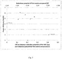
- Fig. 1 showing some materials according to the invention and of the prior art, wherein the power efficiency in lm/W is shown against (a) off-set in reduction potential between the emission layer (EML) host and first matrix compound (ETL matrix) (primary x-axis) and (b) reduction potential of first matrix compound measured against Fc/Fc + in tetrahydrofurane (secondary x-axis).
- EML emission layer
- ETL matrix first matrix compound
- the undoped electron transport layer comprises a first matrix compound.
- the first matrix compound is also described as ETL matrix compound.
- the undoped ETL is substantially free of an alkali organic complex or alkali halide.
- substantially free in this regard means that no alkali organic complex or alkali halide is present in the undoped ETL besides unavoidable impurities.
- Unavoidable impurities are such impurities which cannot be avoided by a person skilled in the art when carefully preparing the inventive devices. For example it is well known that due to diffusion or other similar processes compounds comprised in a layer can get into an adjacent layer during preparing, storing or applying an electronic device. This results in unavoidable impurities.
- the dipole moment of the first matrix compound is selected ⁇ 0 Debye and ⁇ 2.5 Debye, preferably ⁇ 0 Debye and ⁇ 2.3 Debye, more preferably ⁇ 0 Debye and ⁇ 2 Debye.
- the first matrix compound can also be described as non-polar matrix compound.
- the dipole moment is determined by a semi-empirical molecular orbital method.
- the partial charges and atomic positions are obtained using either the DFT functional of Becke and Perdew BP with a def-SV(P) basis or the hybrid functional B3LYP with a def2-TZVP basis set as implemented in the program package TURBOMOLE V6.5. If more than one conformation is viable, the conformation with the lowest total energy is selected to determine the dipole moment.
- the matrix compound may contain a center of inversion I, a horizontal mirror plane, more than one C n axis (n>1), and / or n C 2 perpendicular to C n .
- the matrix compound may contain a dibenzo[c,h]acridine group, a dibenzo[a,j]acridine group, a benzo[c]acridine group, a triaryl borane group, a 2-(benzo[d]oxazol-2-yl)phenoxy metal complex, a 2-(benzo[d]thiazol-2-yl)phenoxy metal complex, a triazine group, a benzothienopyrimidine group or a benzo[k]fluoranthene group.
- a matrix compounds has a dipole moment between 0 and 2.5 Debye, the matrix compound is free of an imidazole group, a phenanthroline group, a phosphine oxide group, an oxadiazole group, a triazole group, a pyrimidine group, a quinazoline group, a benzo[h]quinazoline group or a pyrido[3,2-h]quinazoline group.
- an organic electroluminescent device comprising an anode, a cathode, an emission layer, an undoped electron transport layer comprising a first matrix compound, and an electron injection layer comprising a second matrix compound and an alkali organic complex and/or alkali halide, wherein the undoped electron transport layer and the electron injection layer are arranged between the emission layer and the cathode, wherein the reduction potential of the first matrix compound is less negative than -2.44 V and more negative than -2.03 V, wherein the reduction potential in both cases is measured against Fc/Fc+ in tetrahydrofurane; and the dipole moment of the first matrix compound is selected ⁇ 0 Debye and ⁇ 2.5 Debye and the dipole moment of the second matrix compound is selected > 2.5 and ⁇ 10 Debye.
- the redox potential is determined by cyclic voltammetry with potenioststic device Metrohm PGSTAT30 and software Metrohm Autolab GPES at room temperature.
- the redox potentials given at particular compounds were measured in an argon de-aerated, dry 0.1M THF solution of the tested substance, under argon atmosphere, with 0.1M tetrabutylammonium hexafluorophosphate supporting electrolyte, between platinum working electrodes and with an Ag/AgCl pseudo-standard electrode (Metrohm Silver rod electrode), consisting of a silver wire covered by silver chloride and immersed directly in the measured solution, with the scan rate 100 mV/s.
- the first run was done in the broadest range of the potential set on the working electrodes, and the range was then adjusted within subsequent runs appropriately.
- the final three runs were done with the addition of ferrocene (in 0.1M concentration) as the standard.
- ferrocene in 0.1M concentration
- the reduction potential of the first matrix compound is more negative than -2.03 V and less negative than -2.44 V, preferably more negative than -2.1 V and less negative than -2.4 V, even more preferred more negative than -2.15 V and less negative than - 2.35 V.
- an organic electroluminescent device comprising an anode, a cathode, an emission layer, an undoped electron transport layer comprising a first matrix compound, and an electron injection layer comprising a second matrix compound and an alkali organic complex and/or alkali halide, wherein the undoped electron transport layer and the electron injection layer are arranged between the emission layer and the cathode, wherein the LUMO level of the first matrix compound is more negative than the LUMO level of 9,10-di(naphthalen-2-yl)anthracene (CAS 122648-99-1) and less negative than the LUMO level of 4,4'-bis(4,6-diphenyl-1,3,5-triazin-2-yl)biphenyl (CAS 266349-83-1) when determined under the same conditions; and the dipole moment of the first matrix compound is selected ⁇ 0 Debye and ⁇ 2.5 Debye and the dipole moment of the second matrix compound is selected > 2.5 and
- the LUMO level of 9,10-di(naphthalen-2-yl)anthracene has been determined as -2.36 eV and the LUMO level of 4,4'-bis(4,6-diphenyl-1,3,5-triazin-2-yl)biphenyl is at -2.77 eV.
- the LUMO level of the first matrix compound is more negative than - 2.36 eV and less negative than -2.77 eV, preferably more negative than -2.4 eV and less negative than -2.7 eV, even more preferred, more negative than -2.35 eV and less negative than - 2.65 eV, also preferred more negative than -2.4 eV and less negative than -2.65 eV.
- the first matrix compound is selected from the following compounds or derivatives thereof, the compounds being dibenzo[c,h]acridine, diben-zo[a,j]acridine, benzo[c]acridine, triaryl borane compounds, 2-(benzo[d]oxazol-2-yl)phenoxy metal complex; 2-(benzo[d]thiazol-2-yl)phenoxy metal complex, triazine, benzothienopyrimidine, benzo[k]fluoranthene, perylene or mixtures thereof.
- the electron injection layer further comprises the following compounds or derivatives thereof, the compounds being benzimidazole, phenanthroline; quinazoline, benzo[ h ]quinazoline and pyrido[3,2- h ]quinazoline or mixtures thereof.
- the first matrix compound comprises a triaryl borane compound of formula (I) wherein R 1 , R 3 and R 7 are independently selected from a group consisting of H, D, C 1 -C 16 alkyl and C 1 -C 16 alkoxy; R 2 , R 4 , R 5 and R 6 are independently selected from a group consisting of H, D, C 1 -C 16 alkyl, C 1 -C 16 alkoxy and C 6 -C 20 aryl; Ar 0 is selected from substituted or unsubstituted C 6 -C 20 aryl, wherein, in case that Ar 0 is substituted, the substituents are independently selected from a group consisting of D, C 1 -C 12 alkyl, C 1 -C 16 alkoxy and C 6 -C 20 aryl; and Ar 1 is selected from substituted or unsubstituted C 6 -C 20 arylene, wherein, in case that Ar 1 is substituted, the substituents are independently selected
- Ar 0 is selected from substituted or unsubstituted phenyl or napthyl, wherein, in case that Ar 0 is substituted, the substituents are independently selected from a group consisting of D, C 1 -C 12 alkyl, C 1 -C 16 alkoxy and C 6 -C 20 aryl.
- the first matrix compound comprises a triaryl borane compound of formula (Ia) wherein R 1 , R 3 and R 7 are independently selected from a group consisting of H, D, C 1 -C 16 alkyl and C 1 -C 16 alkoxy; R 2 , R 4 , R 5 and R 6 are independently selected from a group consisting of H, D, C 1 -C 16 alkyl, C 1 -C 16 alkoxy and C 6 -C 20 aryl;
- Ar 1 is selected from substituted or unsubstituted C 6 -C 20 arylene, wherein, in case that Ar 1 is substituted, the substituents are independently selected from a group consisting of D, C 1 -C 12 alkyl, C 1 -C 16 alkoxy and C 6 -C 20 aryl; and
- Ar 2 is selected from a group consisting of H, D, substituted or unsubstituted C 6 -C 40 aryl and groups of the following formulas (IIa) to (IIh), wherein * marks the position in the respective Ar 2 group for binding the Ar 2 to the Ar 1 group, wherein in case that Ar 2 is substituted, the substituents are independently selected from a group consisting of D, halide, C 1 -C 16 alkyl, C 1 -C 16 alkoxy, and C 6 -C 20 aryl, preferably naphthyl, 9-fluorenyl, 2-fluorenyl, 3-fluorenyl and 4-fluorenyl, wherein the C 6 -C 10 aryl may be unsubstituted or substituted with C 1 -C 16 alkyl, C 1 -C 16 heteroalkyl and C 6 -C 40 aryl; wherein Ar 1 and Ar 2 may be further linked via a methylene (-CR 8 R 9 -)
- Ar 2 is selected from the group consisting of phenyl, naphthyl, anthranyl, phenanthryl, pyrenyl, 9-fluorenyl, 2-fluorenyl, 3-fluorenyl, 4-fluorenyl, 5-fluorenyl and formula (IIa) to (IIh).
- R 1 is preferably C 1 -C 12 alkyl, more preferred methyl, or C 1 -C 12 alkoxy, more preferred methoxy, and R 2 to R 7 are each H.
- Ar 1 is preferably phenyl, biphenyl, naphthyl, phenanthryl or anthranyl.
- triaryl borane compounds of formula (Ia) have not yet been described for use in electroluminescent devices, such as that of the invention.
- the first matrix compound comprises a diben-zo[c,h]acridine compound of formula (II) and/or a dibenzo[aj]acridine compound of formula (III) and/or a benzo[c]acridine compound of formula (IV) wherein Ar 3 is independently selected from C 6 -C 20 arylene, preferably phenylene, biphenylene, or fluorenylene; Ar 4 is independently selected from unsubstituted or substituted C 6 -C 40 aryl, preferably phenyl, naphthyl, anthranyl, pyrenyl, or phenanthryl; and in case that Ar 4 is substituted, the one or more substituents may be independently selected from the group consisting of C 1 -C 12 alkyl and C 1 -C 12 heteroalkyl, wherein C 1 -C 5 alkyl is preferred.
- Suitable dibenzo[c,h]acridine compounds are disclosed in EP 2 395 571 .
- Suitable benzo[c]acridine compounds are disclosed in WO 2015/083948 .
- the first matrix compound comprises a diben-zo[c,h]acridine compound substituted with C 6 -C 40 aryl, C 5 -C 40 heteroaryl and/or C 1 -C 12 alkyl groups, preferably 7-(naphthalen-2-yl)dibenzo[c,h]acridine, 7-(3-(pyren-1-yl)phenyl)dibenzo[c,h]acridine, 7-(3-(pyridin-4-yl)phenyl)dibenzo[c,h]acridine.
- the first matrix compound comprises a diben-zo[aj]acridine compound substituted with C 6 -C 40 aryl, C 5 -C 40 heteroaryl and/or C 1 -C 12 alkyl groups, preferably 14-(3-(pyren-1-yl)phenyl)dibenzo[a,j]acridine.
- the first matrix compound comprises a ben-zo[c]acridine compound substituted with C 6 -C 40 aryl, C 5 -C 40 heteroaryl and/or C 1 -C 12 alkyl groups, preferably 7-(3-(pyren-1-yl)phenyl)benzo[c]acridme.
- the first matrix compound comprises a triazine compound of formula (V) wherein Ar 5 is independently selected from unsubstituted or substituted C 6 -C 20 aryl or Ar 5.1 -Ar 5.2 , wherein Ar 5.1 is selected from unsubstituted or substituted C 6 -C 20 arylene and Ar 5,2 is selected from unsubstituted or substituted C 6 -C 20 aryl or unsubstituted and substituted C 5 -C 20 heteroaryl; Ar 6 is selected from unsubstituted or substituted C 6 -C 20 arylene, preferably phenylene, biphenylene, terphenylene, fluorenylene; Ar 7 is independently selected from a group consisting of substituted or unsubstituted aryl, substituted or unsubstituted heteroaryl, the aryl and the heteroaryl having 6 to 40 ring-forming atoms, preferably phenyl, naphthyl, phenant
- Suitable triazine compounds are disclosed in US 2011/284832 , WO 2014/171541 , WO 2015/008866 , WO2015/105313 , JP 2015-074649 A , and JP 2015-126140 , KR 2015/00887 2 .
- the first matrix compound comprises a triazine compound substituted with C 6 -C 40 aryl, C 5 -C 40 heteroaryl and/or C 1 -C 12 alkyl groups, preferably 3-[4-(4,6-di-2-naphthalenyl-1,3,5-triazin-2-yl)phenyl]quinolone, 2-[3-(6'-methyl[2,2'-bipyridin]-5-yl)-5-(9-phenanthrenyl)phenyl]-4,6-diphenyl-1,3,5-triazine, 2-(3-(phenanthren-9-yl)-5-(pyridin-2-yl)phenyl)-4,6-diphenyl-1,3,5-triazine, 2,4-diphenyl-6-(5"'-phenyl-[1,1':3',1":3",1'''':3'',1'''-quinquephenyl]-3-y
- the first matrix compound comprises a 2-(benzo[d]oxazol-2-yl)phenoxy metal complex or 2-(benzo[d]thiazol-2-yl)phenoxy metal complex of formula (VI) wherein M is a metal selected from Al, Zr or Sc; X is selected from O or S; and n is selected from 3 or 4.
- Suitable 2-(benzo[d]oxazol-2-yl)phenoxy metal complex or 2-(benzo[d]thiazol-2-yl)phenoxy metal complex are disclosed in WO 2010/0203 52 .
- the 2-(benzo[d]oxazol-2-yl)phenoxy metal complex is selected from tris(2-(benzo[d]oxazole-2-yl)phenoxy)aluminum and tetra(2-(benzo[d]oxazole-2-yl)phenoxy)zirconium.
- the 2-(benzo[d]thiazol-2-yl)phenoxy metal complex is selected from tris(2-(benzo[d]thiazol-2-yl)phenoxy)aluminum and tetra(2-(benzo[d]oxazole-2-yl)phenoxy)zirconium.
- the first matrix compound comprises a benzothienopyrimidine compound substituted with C 6 -C 40 aryl, C 5 -C 40 heteroaryl and/or C 1 -C 12 alkyl groups, preferably 2-phenyl-4-(4',5',6'-triphenyl-[1,1':2',1":3",1'''-quaterphenyl]-3'''-yl)benzo[4,5]thieno[3,2-d]pyrimidine.
- a benzothienopyrimidine compound substituted with C 6 -C 40 aryl, C 5 -C 40 heteroaryl and/or C 1 -C 12 alkyl groups, preferably 2-phenyl-4-(4',5',6'-triphenyl-[1,1':2',1":3",1'''-quaterphenyl]-3'''-yl)benzo[4,5]thieno[3,2-d]pyrimidine.
- Suitable benzothienopyrimidine compounds are disclosed in W 2015/010536 .
- the first matrix compound comprises a ben-zo[k]fluoranthene compound substituted with C 6 -C 40 aryl, C 5 -C 40 heteroaryl and/or C 1 -C 12 alkyl groups, preferably 7, 12-diphenylbenzo[k]fluoranthene.
- Suitable benzo[k]fluoranthene compounds are disclosed in JP10189247 A2 .
- the first matrix compound comprises a perylene compound substituted with C 6 -C 40 aryl, C 5 -C 40 heteroaryl and/or C 1 -C 12 alkyl groups, preferably 3,9-bis([1,1'-biphenyl]-2-yl)perylene, 3,9-di(naphthalene-2-yl)perylene or 3,10-di(naphthalene-2-yl)perylene.
- Suitable perylene compounds are disclosed in US2007202354 .
- the first matrix compound may preferably be selected from one of the following compounds of Table 1.
- the electron injection layer comprises a second matrix compound and an alkali organic complex and/or alkali halide.
- the second matrix compound is also described as EIL matrix compound.
- the dipole moment of the second matrix compound is selected > 2.5 Debye and ⁇ 10 Debye, preferably > 3 and ⁇ 5 Debye, even more preferred > 2.5 and less than 4 Debye.
- the second matrix compound can also be described as non-polar matrix compound.
- the dipole moment is calculated using the method described for the first matrix compound.
- the matrix compound may be described by one of the following symmetry groups: C 1 , C n , C nv , or C s .
- the matrix compound may contain an imidazole group, a phenanthroline group, a phosphine oxide group, an oxadiazole group, a triazole group, a pyrimidine group, a quinazoline group, a benzo[h]quinazoline group or a pyrido[3,2-h]quinazoline group.
- the second matrix compound comprises a phosphine oxide compound substituted with C 6 -C 40 aryl, C 5 -C 40 heteroaryl and/or C 1 -C 12 alkyl groups, preferably (3-(dibenzo[c,h]acridin-7-yl)phenyl)diphenylphosphine oxide, 3 -phenyl-3H-benzo [b]dinaphtho[2,1-d:1',2'-f]phosphepine-3-oxide, phenyldi(pyren-1-yl)phosphine oxide, bis(4-(anthracen-9-yl)phenyl)(phenyl)phosphine oxide, (3-(9,10-di(naphthalen-2-yl)anthracen-2-yl)phenyl)diphenylphosphine oxide, phenyldi(pyren-1-yl)phosphine oxide, diphenyl(5-(pyren-1-
- Diphenylphosphine oxide compounds that can be used as second matrix materials are disclosed in EP 2395571 A1 , WO2013079217 A1 , EP 13187905 , EP13199361 and JP2002063989 A1 ,
- Extraordinary preferred second matrix compounds are that of the following structures of Table 2.
- the lithium halide can be selected from the group comprising LiF, LiCl, LiBr or LiJ, and preferably LiF.
- the alkali organic complex can be a lithium organic complex and preferably the lithium organic complex can be selected from the group comprising a lithium quinolate, a lithium borate, a lithium phenolate, a lithium pyridinolate or a lithium Schiff base and lithium fluoride, preferably a lithium 2-(diphenylphosphoryl)-phenolate, lithium tetra(1H-pyrazol-1-yl)borate, a lithium quinolate of formula (III), a lithium 2-(pyridin-2-yl)phenolate and LiF, and more preferred selected from the group comprising a lithium 2-(diphenylphosphoryl)-phenolate, lithium tetra(1H-pyrazol-1-yl)borate, a lithium quinolate of formula (III) and a lithium 2-(pyridin-2-yl)phenolate.
- the lithium organic complex can be selected from the group comprising a lithium quinolate, a lithium borate, a lithium phenolate, a lithium pyridinolate or
- the alkali organic complex is a lithium organic complex and/or the alkali halide is lithium halide.
- the organic ligand of the lithium organic complex can be a borate based organic ligand.
- the lithium organic complex is a compound of formula (VII) wherein M is an alkali metal ion, each of A 1 -A 4 is independently selected from substituted or unsubstituted C 6 -C 20 aryl or substituted or unsubstituted C 2 -C 26 heteroaryl.
- the alkali organic complex is a complex of formula (VIII) wherein each of A 1 -A 4 is independently selected from substituted or unsubstituted C 6 -C 20 aryl or substituted or unsubstituted C 2 -C 20 heteroaryl.
- the lithium organic complex is a lithium tetra(1H-pyrazol-1-yl)borate.
- Borate based organic ligands that can be suitable used are disclosed in WO 2013079676 A1 .
- the organic ligand of the lithium organic complex can be a phenolate ligand.
- the organic ligand of the lithium organic complex can be a phosphoryl phenolate ligand.
- the lithium organic complex is a phosphoryl phenolate compound of formula (IX): wherein A 5 is a C 6 -C 20 arylene and each of A 6 -A 7 is independently selected from a C 6 -C 20 aryl, wherein A 5 , A 6 and A 7 may be unsubstituted or substituted with groups comprising C and H or with a further LiO group, provided that the given C count in an aryl or arylene group includes also all substituents present on the said group.
- the lithium organic complex is a lithium 2-(diphenylphosphoryl)phenolate. Phenolate ligands that can be suitable used are disclosed in WO 2013079678 A1 .
- phenolate ligands can be selected from the group comprising pyridinolate, preferably 2-(diphenylphosphoryl)pyridin-3-olate.
- Pyridine phenolate ligands that can be suitable used are disclosed in JP 2008195623 .
- phenolate ligands can be selected from the group comprising imidazole phenolates, preferably 2-(1-phenyl-1H-benzo[d]imidazol-2-yl)phenolate.
- imidazole phenolates preferably 2-(1-phenyl-1H-benzo[d]imidazol-2-yl)phenolate.
- Imidazol phenolate ligands that can be suitable used are disclosed in JP 200129 593 .
- phenolate ligands can be selected from the group comprising oxazol phenolates, preferably 2-(benzo[d]oxazol-2-yl)phenolate.
- Oxazol phenolate ligands that can be suitable used are disclosed in US 2003016571 1 .
- the organic ligand of the lithium organic complex can be a phosphoryl heteroaryloate ligand.
- the lithium organic complex is a phosphoryl heteroaryloate compound of formula (X): wherein A 8 , A 9 and A 10 are independently selected from C 1 -C 30 -alkyl, C 3 -C 30 -cycloalkyl, C 2 -C 30 -heteroalkyl, C 6 -C 36 -aryl, C 2 -C 30 -heteroaryl, C 1 -C 30 -alkoxy, C 3 -C 30 -cycloalkyloxy, C 6 -C 30 -aryloxy, and from structural unit having general formula E-Z-, wherein Z is a spacer unit containing trivalent nitrogen atom bearing a lone electron pair, wherein the spacer unit has a structure which allows formation of a 5-, 6- or 7-membered chelate ring with the metal cation, wherein the chelate ring comprises the oxygen atom of the phosphine oxide group and trivalent nitrogen atom of the spacer unit coordinated to the
- the lithium organic complex is a lithium 2-(diphenylphosphoryl)pyridin-3-olate.
- Heteroarylolate ligands that can be suitable used are disclosed in EP 27243 88 .
- the organic ligand of the alkali organic complex can be selected from a borate ligand and a phosphoryl phenolate ligand and a heteroarylolate ligand.
- the organic ligand of the alkali organic complex is selected from a borate ligand and a phosphoryl phenolate ligand.
- the lithium organic complex can be selected from the group comprising a lithium quinolate, a lithium borate, a lithium phenolate, a lithium pyridinolate or a lithium Schiff base; preferably
- the organic ligand of the lithium organic complex can be a phenolate ligand, Preferably the lithium organic complex is a lithium 2-(diphenylphosphoryl)phenolate.
- Phenolate ligands that can be suitable used are disclosed in WO 2013079678 A1 .
- phenolate ligands can be selected from the group comprising pyridinolate, preferably 2-(diphenylphosphoryl)pyridin-3-olate.
- Pyridine phenolate ligands that can be suitable used are disclosed in JP 2008 95623 .
- phenolate ligands can be selected from the group comprising imidazol phenolates, preferably 2-(1-phenyl-1H-benzo[d]imidazol-2-yl)phenolate.
- Imidazole phenolate ligands that can be suitable used are disclosed in JP 200129 593 .
- phenolate ligands can be selected from the group comprising oxazol phenolates, preferably 2-(benzo[d]oxazol-2-yl)phenolate.
- Oxazol phenolate ligands that can be suitable used are disclosed in US 2003016571 1 .
- Lithium Schiff base organic complexes can be use. Lithium Schiff base organic complexes that can be suitable used having the structure 100, 101, 102 or 103:
- Suitable organic ligands to form a lithium organic complex that can be used for the electron injection layer are disclosed for example in US 2014/0048792 and Kathirgamanathan, Poopathy; Arkley, Vincent; Surendrakumar, Sivagnanasundram; Chan, Yun F.; Ravichandran, Seenivasagam; Ganeshamurugan, Subramaniam; Kumaraverl, Muttulingam; Antipan-Lara, Juan; Paramaswara, Gnanamolly; Reddy, Vanga R., Digest of Technical Papers - Society for Information Display International Symposium (2010), 41(Bk. 1), 465-468 .
- the organic electroluminescent device according to the present invention is an organic light-emitting diode (OLED).
- OLED organic light-emitting diode
- the organic light-emitting diode may be a bottom- or top-emitting diode.
- the thickness of the undoped electron transport layer is at least two times the thickness of the electron injection layer, preferably the thickness of the undoped electron transport layer is at least three times the thickness of the electron injection layer, even more preferred the thickness of the undoped electron transport layer is at least four times the thickness of the electron injection layer, also preferred the thickness of the undoped electron transport layer is at least eight times the thickness of the electron injection layer.
- the maximum thickness of the undoped electron injection layer is 200 nm.
- the emission layer comprises a fluorescent blue emitter.
- the organic electroluminescent device is a fluorescent blue device.
- the emission layer further comprises an anthracene matrix compound substituted with C 6 -C 40 aryl, C 5 -C 40 heteroaryl and/or C 1 -C 12 alkyl groups.
- the organic electroluminescent device according to the present invention may comprise more than one emission layer, preferably two or three emission layers.
- the organic electroluminescent device comprises a charge generation layer (CGL).
- CGL charge generation layer
- the external quantum efficiency also named EQE, is measured in percent (%).
- the power efficiency also named PEff, is measured in lumen per Watt (lm/W).
- the lifetime, also named LT, between starting brightness and 97 % of the original brightness is measured in hours (h).
- the voltage also named V, is measured in Volt (V) at 10 milliAmpere per square centimeter (mA/cm2) in bottom emission devices and at 15 mA/cm2 in top emission devices.
- the color space is described by coordinates CIE-x and CIE-y (International Commission on Illumination 1931).
- CIE-x International Commission on Illumination 1931
- CIE-y International Commission on Illumination 1931
- a smaller CIE-y denotes a deeper blue color.
- the highest occupied molecular orbital, also named HOMO, and lowest unoccupied molecular orbital, also named LUMO, are measured in electron volt (eV).
- OLED organic light-emitting diode
- electron transport layer stack as used in the specification comprises at least two electron transport layers or at least three electron transport layers.
- weight percent As used herein, “weight percent”, “wt.-%”, “percent by weight”, “% by weight”, and variations thereof refer to a composition, component, substance or agent as the weight of that component, substance or agent of the respective electron transport layer divided by the total weight of the respective electron transport layer thereof and multiplied by 100. It is understood that the total weight percent amount of all components, substances and agents of the respective electron transport layer are selected such that it does not exceed 100 wt.-%.
- the term "free of” means that the so called “free off” undoped electron transport layer may comprise of about 5 wt.-% or less of a dopant, alkali halide and/or a alkali organic complex, preferably about 0.5 wt.-% or less, and more preferably about 0.05 wt.-% or less, and even more preferably about 0.005 wt.-% or less of a dopant, alkali halide and/or alkali organic complex and most preferred is free of a dopant, alkali halide and/or a alkali organic complex.
- alkyl as used herein shall encompass linear as well as well as branched alkyl.
- C 3 -alkyl may be selected from n-propyl and iso-propyl.
- C 4 -alkyl encompasses n-butyl, sec-butyl and t-butyl.
- alkoxy as used herein shall encompass linear and branched alkoxy.
- C 3 -alkoxy encompasses n-propoxy and iso-propoxy.
- the subscripted number n in C n relates to the total number of carbon atoms in the respective alkyl, alkoxy, aryl or heteroaryl group.
- aryl as used herein shall encompass phenyl (C 6 -aryl), fused aromatics, such as naphthalene, anthracene, phenanthrene, tetracene, etc. Further encompassed are biphenyl or oligo- or polyphenyls, such as terphenyl etc. Further encompassed shall be any further aromatic hydrocarbon substituents, such as fluorenyl etc.
- heteroaryl as used herein shall encompass any aryl compound as defined above in which one or more of the carbon atoms comprised in the aromatic ring system is substituted by a hetero atom, preferably N, O, or S.
- aryl as used herein may be synonymous to the term arylene.
- aryl is arylene in this case.
- the aryl group may comprise one or more substituents.
- organic electroluminescent devices may comprise one or more of the following components, selected from substrate, anode, hole injection layer, emission layer, hole blocking layer and cathode as defined below.
- the substrate may be any substrate that is commonly used in manufacturing of organic light-emitting diodes. If light is emitted through the substrate, the substrate may be a transparent material, for example a glass substrate or a transparent plastic substrate, having excellent mechanical strength, thermal stability, transparency, surface smoothness, ease of handling, and waterproofness. If light is emitted through the top surface, the substrate may be a transparent or non-transparent material, for example a glass substrate, a plastic substrate, a metal substrate or a silicon substrate.
- the anode may be formed by depositing or sputtering a compound that is used to form the anode.
- the compound used to form the anode may be a high work-function compound, so as to facilitate hole injection.
- the anode material may also be selected from a low work function material (i.e. Aluminum).
- the anode may be a transparent or reflective electrode.
- Transparent conductive compounds such as indium tin oxide (ITO), indium zinc oxide (IZO), tin-dioxide (SnO 2 ), and zinc oxide (ZnO), may be used to form the anode 120.
- the anode 120 may also be formed using magnesium (Mg), aluminum (Al), aluminum-lithium (Al-Li), calcium (Ca), magnesium-indium (Mg-In), magnesium-silver (Mg-Ag), silver (Ag), gold (Au), or the like.
- the hole injection layer (HIL) 130 may be formed on the anode 120 by vacuum deposition, spin coating, printing, casting, slot-die coating, Langmuir-Blodgett (LB) deposition, or the like.
- the deposition conditions may vary according to the compound that is used to form the HIL 130, and the desired structure and thermal properties of the HIL 130. In general, however, conditions for vacuum deposition may include a deposition temperature of 100° C to 500° C, a pressure of 10 -8 to 10 -3 Torr (1 Torr equals 133.322 Pa), and a deposition rate of 0.1 to 10 nm/sec.
- coating conditions may vary according to a compound that is used to form the HIL 130, and the desired structure and thermal properties of the HIL 130.
- the coating conditions may include a coating speed of about 2000 rpm to about 5000 rpm, and a thermal treatment temperature of about 80° C to about 200° C. Thermal treatment removes a solvent after the coating is performed.
- the HIL 130 may be formed of any compound that is commonly used to form an HIL.
- examples of compounds that may be used to form the HIL 130 include a phthalocyanine compound, such as copper phthalocyanine (CuPc), 4,4',4"-tris (3-methylphenylphenylamino) triphenylamine (m-MTDATA), TDATA, 2T-NATA, polyaniline/dodecylbenzenesulfonic acid (Pani/DBSA), poly(3,4-ethylenedioxythiophene)/poly(4-styrenesulfonate) (PEDOT/PSS), polyaniline/camphor sulfonic acid (Pani/CSA), and polyaniline)/poly(4-styrenesulfonate (PANI/PSS).
- CuPc copper phthalocyanine
- m-MTDATA 4,4',4"-tris (3-methylphenylphenylamino) triphenylamine
- the HIL 130 may be a pure layer of p-dopant or may be selected from a hole-transporting matrix compound doped with a p-dopant.
- CuPc copper phthalocyanine
- F4TCNQ tetrafluoro-tetracyanoquinonedimethane
- ZnPc
- PD1 2,2'-(perfluoronaphthalen-2,6-diylidene) dimalononitrile
- PD2 2,2',2"-(cyclopropane-1,2,3-triylidene)tris(2-(p-cyanotetrafluorophenyl)acetonitrile) (PD2).
- Dopant concentrations can be selected from 1 to 20 wt.-%, more preferably from 3 wt.-% to 10 wt.-%.
- the thickness of the HIL 130 may be in the range of about 1 nm to about 100 nm, and for example, about 1 nm to about 25 nm. When the thickness of the HIL 130 is within this range, the HIL 130 may have excellent hole injecting characteristics, without a substantial increase in driving voltage.
- the hole transport layer (HTL) 140 may be formed on the HIL 130 by vacuum deposition, spin coating, slot-die coating, printing, casting, Langmuir-Blodgett (LB) deposition, or the like.
- the conditions for deposition and coating may be similar to those for the formation of the HIL 130.
- the conditions for the vacuum or solution deposition may vary, according to the compound that is used to form the HTL 140.
- the HTL 140 may be formed of any compound that is commonly used to form a HTL.
- Compound that can be suitably used is disclosed for example in Yasuhiko Shirota and Hiroshi Kageyama, Chem. Rev. 2007, 107, 953-1010 .
- a carbazole derivative such as N-phenylcarbazole or polyvinylcarbazole
- an amine derivative having an aromatic condensation ring such as N,N'-bis(3-methylphenyl)-N,N'-diphenyl-[1,1-biphenyl]-4,4'-diamine (TPD), or N,N'-di(naphthalen-1-yl)-N,N'-diphenyl benzydine (alpha -NPD)
- TPD N,N'-di(naphthalen-1-yl)-N,N'-diphenyl benzydine
- TCTA triphenylamine-based compound
- TCTA can transport holes and inhibit excitons from being diffused into the EML.
- the thickness of the HTL 140 may be in the range of about 5 nm to about 250 nm, preferably, about 10 nm to about 200 nm, further about 20 nm to about 190 nm, further about 40 nm to about 180 nm, further about 60 nm to about 170 nm, further about 80 nm to about 160 nm, further about 100 nm to about 160 nm, further about 120 nm to about 140 nm.
- a preferred thickness of the HTL 140 may be 170 nm to 200 nm.
- the HTL 140 may have excellent hole transporting characteristics, without a substantial increase in driving voltage.
- Emission laver Emission laver
- the EML 150 may be formed on the HTL by vacuum deposition, spin coating, slot-die coating, printing, casting, LB, or the like.
- the conditions for deposition and coating may be similar to those for the formation of the HIL. However, the conditions for deposition and coating may vary, according to the compound that is used to form the EML.
- the emission layer may be formed of a combination of a host and a dopant.
- Example of the host are Alq3, 4,4'-N,N'- dicarbazole-biphenyl (CBP), poly(n-vinylcarbazole) (PVK), 9,10-di(naphthalene-2-yl)anthracene (ADN), 4,4',4"-Tris(carbazol-9-yl)-triphenylamine (TCTA), 1,3,5-tris(N-phenylbenzimidazole-2-yl)benzene (TPBI), 3-tert-butyl-9,10-di-2-naphthylanthracenee (TBADN), distyrylarylene (DSA), Bis(2-(2-hydroxyphenyl)benzo-thiazolate)zinc (Zn(BTZ) 2), E3 below, ADN, Compound 1 below, and Compound 2 below.
- CBP 4,4'-N,N'-
- anthracene-based hosts represented by Formula 400 below:
- Ar 111 and Ar 112 may be each independently a substituted or unsubstituted C 6 -C 60 arylene group;
- Ar 113 to Ar 116 may be each independently a substituted or unsubstituted C 1 -C 10 alkyl group or a substituted or unsubstituted C 6 -C 60 aryl group;
- g, h, i, and j may be each independently an integer from 0 to 4.
- Ar 111 and Ar 112 in Formula 400 may be each independently one of a phenylene group, a naphthylene group, a phenanthrenylene group, or a pyrenylene group; or a phenylene group, a naphthylene group, a phenanthrenylene group, a fluorenyl group, or a pyrenylene group, each substituted with at least one of a phenyl group, a naphthyl group, or an anthryl group.
- g, h, i, and j may be each independently an integer of 0, 1, or 2.
- Ar 113 to Ar 116 may be each independently one of a C 1 -C 10 alkyl group substituted with at least one of a phenyl group, a naphthyl group, or an anthryl group; a phenyl group, a naphthyl group, an anthryl group, a pyrenyl group, a phenanthrenyl group, or a fluorenyl group; a phenyl group, a naphthyl group, an anthryl group, a pyrenyl group, a phenanthrenyl group, or a fluorenyl group, each substituted with at least one of a deuterium atom, a halogen atom, a hydroxyl group, a cyano group, a nitro group, an amino group, an amidino group, a hydrazine group, a hydrazone group, a carboxyl group or a salt thereof, a sulfonic acid
- the dopant may be a phosphorescent or fluorescent emitter. Phosphorescent emitters are preferred due to their higher efficiency
- red dopant examples include PtOEP, Ir(piq) 3, and Btp 21r(acac), but are not limited thereto. These compounds are phosphorescent emitters, however, fluorescent red dopants could also be used.
- Compound 3 is an example of a fluorescent green emitter and the structure is shown below.
- Examples of a phosphorescent blue dopant are F 2 Irpic, (F 2 ppy) 2 Ir(tmd) and Ir(dfppz) 3, ter-fluorene, the structures are shown below.
- 4.4'-bis(4-diphenyl amiostyryl)biphenyl (DPAVBi), 2,5,8,11-tetra-tert-butyl perylene (TBPe), and Compound 4 below are examples of fluorescent blue dopants.
- the amount of the dopant may be in the range of about 0.01 to about 50 parts by weight, based on 100 parts by weight of the host.
- the EML may have a thickness of about 10 nm to about 100 nm, for example, about 20 nm to about 60 nm. When the thickness of the EML is within this range, the EML may have excellent light emission, without a substantial increase in driving voltage.
- the emission layer may be formed of a light-emitting polymer which emits fluorescent or phosphorescent light.
- the light-emitting polymer may comprise a conjugated backbone comprising arene groups or a non-conjugated backbone.
- the conjugated backbone comprises fluorene, phenanthrene and/or triarylamine groups. If the light-emitting polymer emits light from the triplet state, the polymer may comprise phosphorescent metal complexes in the backbone or attached to the backbone.
- HBL Hole blocking layer
- a hole blocking layer may be formed on the EML, by using vacuum deposition, spin coating, slot-die coating, printing, casting, LB deposition, or the like, in order to prevent the diffusion of triplet excitons or holes into the ETL.
- the conditions for deposition and coating may be similar to those for the formation of the HIL. However, the conditions for deposition and coating may vary, according to the compound that is used to form the HBL. Any compound that is commonly used to form a HBL may be used. Examples of compounds for forming the HBL include an oxadiazole derivative, a triazole derivative, and a phenanthroline derivative.
- the HBL may have a thickness of about 5 nm to about 100 nm, for example, about 10 nm to about 30 nm. When the thickness of the HBL is within this range, the HBL may have excellent hole-blocking properties, without a substantial increase in driving voltage.
- the cathode is formed on the EIL.
- the cathode may be a cathode, which is an electron-injecting electrode.
- the cathode may be formed of a metal, an alloy, an electrically conductive compound, or a mixture thereof.
- the cathode may have a low work function.
- the cathode may be formed of lithium (Li), magnesium (Mg), aluminum (Al), aluminum (Al)-lithium (Li), calcium (Ca), barium (Ba), ytterbium (Yb), magnesium (Mg)-indium (In), magnesium (Mg)-silver (Ag), or the like.
- the cathode may be formed of a transparent conductive material, such as ITO or IZO.
- the thickness of the cathode may be in the range of about 5 nm to 1000 nm, for example, in the range of 10 nm to 100 nm.
- the cathode When the cathode is in the range of 5 nm to 50 nm, the electrode will transparent even if a metal or metal alloy is used.
- the cathode is not an electron injection layer or electron transport layer.
- the injection and transport of the electrons may be controlled, and the holes may be efficiently blocked.
- the OLED may have long lifetime.
- an organic electroluminescent device comprising: a substrate; a anode formed on the substrate; a hole injection layer, a hole transport layer, an emission layer, an undoped electron transport layer, an electron injection layer, and a cathode.
- an organic electroluminescent device comprising: a substrate; a anode formed on the substrate; a hole injection layer, a hole transport layer, an emission layer, a hole blocking layer, an undoped electron transport layer, an electron injection layer, and a cathode.
- the inventive organic electroluminescent device solve the problem underlying the present invention by being superior over the organic electroluminescent devices known in the art, in particular with respect to power efficiency.
- the inventors have surprisingly found that particular good performance can be achieved when using the organic electroluminescent device as a fluorescent blue device.
- the specific arrangements mentioned herein as preferred were found to be particularly advantageous.
- first element when a first element is referred to as being formed or disposed "on" a second element, the first element can be disposed directly on the second element, or one or more other elements may be disposed there between.
- first element when referred to as being formed or disposed "directly on” a second element, no other elements are disposed there between.
- Fig. 1 is a graph wherein the power efficiency in lm/W is plotted (a) against off-set between reduction potential of the EML host and reduction potential of the first matrix compound in Volt (primary x-axis) and (b) the reduction potential of the first matrix compound measured against Fc/Fc + in tetrahydrofurane in Volt (secondary x-axis).
- a small off-set in reduction potential of the EML host and the first matrix compound leads to low power efficiency.
- a very large off-set between reduction potential of the EML host and first matrix compound results in low power efficiency.
- a polar first matrix compound also leads to poor performance. Surprisingly, it was found that the power efficiency is significantly increased if a small off-set in reduction potential between the EML host and first matrix compound is present and the first matrix compound is a polar compound.
- Fig. 2 is a schematic sectional view of an organic electroluminescent device (OLED) 100, according to an exemplary embodiment of the present invention.
- the OLED 100 includes a substrate 110, a first electrode 120, a hole injection layer (HIL) 130, a hole transport layer (HTL) 140, an emission layer (EML) 150, an undoped electron transport layer (ETL) 161.
- the undoped electron transport layer (ETL) 161 is formed directly on the EML 150.
- the electron injection layer (EIL) 180 is formed directly on the ETL.
- a cathode 190 is disposed on the electron injection layer 180.
- Fig. 3 is a schematic sectional view of an OLED 100, according to another exemplary embodiment of the present invention.
- Fig. 3 differs from Fig. 2 in that the OLED 100 of Fig. 3 comprises a hole blocking layer (HBL) 155.
- HBL hole blocking layer
- an OLED of the present invention is started with a substrate 110 onto which an anode 120 is formed, on the anode 120, an hole injection layer 130, hole transport layer 140, an emission layer 150, optional a hole blocking layer 155, at least one electron transport layer 161, at least one electron injection layer 180, and a cathode 190 are formed, in that order or the other way around.
- a sealing layer may further be formed on the cathodes 190, in order to seal the OLEDs 100.
- various other modifications may be applied thereto.
- Examples 1 to 5 and comparative examples 1 to 4 a 15 ⁇ /cm 2 glass substrate (available from Corning Co.) with 100 nm Ag was cut to a size of 50 mm x 50 mm x 0.7 mm, ultrasonically cleaned with isopropyl alcohol for 5 minutes and then with pure water for 5 minutes, and cleaned again with UV ozone for 30 minutes, to prepare a first electrode.
- a 15 ⁇ /cm 2 glass substrate available from Corning Co.
- 92 wt.-% of a hole transport matrix doped with 8 wt.-% and 8 wt.-% of 2,2',2"-(cyclopropane-1,2,3-triylidene)tris(2-(p-cyanotetrafluorophenyl)acetonitrile) was vacuum deposited on the ITO electrode, to form a HIL having a thickness of 10 nm.
- the hole transport matrix was vacuum deposited on the HIL, to form a HTL having a thickness of 120 nm.
- the undoped electron transport layer is formed by depositing a matrix compound according to Example 1 to Example 5 and Comparative examples 1 to 4, see Table 6.
- the electron injection layer is formed by deposing 2-(4-(9,10-di(naphthalen-2-yl)anthracen-2-y1)phenyl)-1-phenyl-1H-benzo[d]imidazole (CAS 561064-11-7) doped with 30 wt.-% LiQ (Comparative Example 1) or 3-Phenyl-3H-benzo[b]dinaphtho[2,1-d:1',2'-f]phosphepine-3-oxide (EIM-11), doped with 30 wt.-% Lithium tetra(1H-pyrazol-1-yl)borate (Li-1) (Example 1 to 5 and Comparative examples 2 to 4) to form a layer as specified in Table 6.
- the cathode was evaporated at ultra-high vacuum of 10 -7 bar. Therefore, a thermal single co-evaporation of one or several metals was performed with a rate of 0, 1 to 10 nm/s (0.01 to 1 ⁇ /s) in order to generate a homogeneous cathode with a thickness of 5 to 1000 nm.
- the cathode was formed from 100 nm aluminum.
- the OLED stack is protected from ambient conditions by encapsulation of the device with a glass slide. Thereby, a cavity is formed, which includes a getter material for further protection.
- the current efficiency is measured under ambient conditions (20°C). Current voltage measurements are performed using a Keithley 2400 sourcemeter, and recorded in V. At 10 mA/cm 2 for bottom emission and 15 mA/cm 2 for top emission devices, a calibrated spectrometer CAS140 from Instrument Systems is used for measurement of CIE coordinates and brightness in Candela. Lifetime LT of the device is measured at ambient conditions (20°C) and 15 mA/cm 2 , using a Keithley 2400 sourcemeter, and recorded in hours. The brightness of the device is measured using a calibrated photo diode. The lifetime LT is defined as the time till the brightness of the device is reduced to 97 % of its initial value.
- the light output in external efficiency EQE and power efficiency (1m/W efficiency) are dertermined at 10 mA/cm 2 for bottom emission devices and 15 mA/cm 2 for top emission devices.
- the light output of the device is measured using a calibrated photodiode.
- the emission is predominately Lambertian and quantified in percent external quantum efficiency (EQE) and power efficiency in 1m/W.
- EQE percent external quantum efficiency
- anthracene compound ADN (9,10-di(naphthalen-2-yl)anthracene, CAS 122648-99-1) is tested as first matrix compound.
- the reduction potential is -2.44 V against Fc/Fc + in tetrahydrofurane and the dipole moment is 0.01 Debye.
- the reduction potential and LUMO level of the first matrix compound are the same as of the EML host.
- the EIL comprises benzimidazole compound EIM-1 and lithium organic complex LiQ.
- the power efficiency is 3.2 1m/W (Table 6).
- first matrix compound ADN is tested with an EIL comprising phosphine oxide compound EIM-11 and lithium organic complex Li-1.
- the power efficiency is improved to 4.1 lm/W.
- the reduction potential is -2.03 V against Fc/Fc + in tetrahydrofurane and the dipole moment is 0.03 Debye.
- the EIL composition is selected the same as in comparative example 2.
- the power efficiency is reduced to 2 lm/W.
- a very large off-set in reduction potential and LUMO of the EML host compared to the ETL matrix has a detrimental effect on power efficiency.
- phosphine oxide compound EIM-9 with a reduction potential of - 2.2 V against Fc/Fc + in tetrahydrofurane is tested as ETL matrix.
- the dipole moment of this compound is 4 Debye. Therefore, this compound is a polar compound in the sense of the present invention.
- the EIL composition is selected the same as in comparative examples 2.
- the power efficiency is reduced compared to comparative example 2, 2.4 V against 4.1 V for comparative example 2 (Table 6). Even though the off-set in reduction potential between the EML matrix and ETL matrix is within the desired range, the high dipole moment of the ETL matrix compound results in low power efficiency.
- Example 1 triaryl borane compound ETM-3 is tested with the same EIL composition as in comparative example 2.
- the reduction potential of ETM-3 is -2.33 V against Fc/Fc + in tetrahydrofurane and the dipole moment is ⁇ 2.5 Debye.
- the power efficiency is improved from 4.1 to 4.85 lm/W.
- Example 2 a triaryl borane compound with a deeper LUMO compared to Example 1 is tested.
- the reduction potential of ETM-1 is -2.31 V against Fc/Fc + in tetrahydrofurane and the dipole moment is 0.14 Debye.
- the power efficiency is further improved from 4.85 to 6.1 lm/W.
- Example 3 triazine compound ETM-28 is tested with the same EIL composition as in comparative example 2.
- the reduction potential is -2.17 V against Fc/Fc + in tetrahydrofurane and the dipole moment is 1.76 Debye.
- the power efficiency is improved from 4.1 lm/W in comparative example 2 to 5.3 lm/W in Example 3.
- Example 5 dibenzo[c,h]acridine compound ETM-15 is tested with the same EIL composition as in comparative example 2.
- the reduction potential is -2.26 V against Fc/Fc + in tetrahydrofurane and the dipole moment is between 1.5 and 2 Debye.
- the power efficiency is improved from 4.1 lm/W in comparative example 2 to 5.7 lm/W in Example 5.
- Example 6 tris(2-(benzo[d]thiazol-2-yl)phenoxy)aluminum metal complex ETM-34 is tested with the same EIL composition as in comparative example 2.
- the reduction potential is -2.21 V against Fc/Fc + in tetrahydrofurane and the dipole moment is ⁇ 2.5 Debye.
- the power efficiency is improved from 4.1 lm/W in comparative example 2 to 4.9 lm/W in Example 6.
- lm/W efficiency a significant improvement in power efficiency (lm/W efficiency) has been achieved for a wide range of first matrix compound classes with a reduction potential less negative than the reduction potential of 9,10-di(naphthalen-2-yl)anthracene (CAS 122648-99-1) and more negative than the reduction potential of 4,4'-bis(4,6-diphenyl-1,3,5-triazin-2-yl)biphenyl (CAS 266349-83-1) and a dipole moment between ⁇ 0 Debye and ⁇ 2.5 Debye.
- OLED organic light-emitting diode
- EML emission layer
- An organic light-emitting diode (OLED) comprising more than one emission layer is also described as a tandem OLED or stacked OLED.
- OLED organic light-emitting diode
- a device comprising organic light-emitting diodes (OLED) is for example a display or a lighting panel.
Description
- The present invention relates to an organic electroluminescent device.
- Organic light-emitting diodes (OLEDs), which are self-emitting devices, have a wide viewing angle, excellent contrast, quick response, high brightness, excellent driving voltage characteristics, and color reproduction. A typical OLED includes an anode, a hole transport layer (HTL), an emission layer (EML), an electron transport layer (ETL), and a cathode, which are sequentially stacked on a substrate. In this regard, the HTL, the EML, and the ETL are thin films formed from organic and / or organometallic compounds.
- When a voltage is applied to the anode and the cathode, holes injected from the anode move to the EML, via the HTL, and electrons injected from the cathode move to the EML, via the ETL. The holes and electrons recombine in the EML to generate excitons. When the excitons drop from an excited state to a ground state, light is emitted. The injection and flow of holes and electrons should be balanced, so that an OLED having the above-described structure has excellent efficiency.
-
JP 2003-338377 - To improve electron injection further, EILs doped with Li organic complexes have been developed, in particular benzimidazole-based matrix compound doped with LiQ, phenanthroline-based matrix compound doped with LiQ or phosphine oxide-based matrix compound doped with Li organic complex.
-
US2007252521 teaches that the LUMO off-set between the emission layer and ETL should be selected as small as possible. Ideally, no LUMO off-set between the EML and ETL should be present. -
JP 2003-338377 A - Hoe Min Kim et al., Molecular Crystals and Liquid Crystals, 2011, 538(1), 53, discloses a mixed electron transport structure red phosphorescent organic light-emitting diode.
- However, the power efficiency of organic electroluminescent devices still remains to be improved. The power efficiency is of particular importance for commercial products as it takes into account the human eye response. The higher the power efficiency, the more effectively power is converted into light output that is visible to the human eye.
- Therefore, it is the object of the present invention to provide organic electroluminescent devices overcoming drawbacks of the prior art, in particular featuring increased power efficiency measured in lumen per Watt (lm/W), in particular of fluorescent blue devices, such as OLEDs.
- The above object is achieved in accordance with the subject-matter of the independent claim.
- Preferred embodiments result from the sub-claims.
- According to one aspect, there is provided an organic electroluminescent device comprising an anode, a cathode, an emission layer, an undoped electron transport layer comprising a first matrix compound, and an electron injection layer comprising a second matrix compound and an alkali organic complex and/or alkali halide,
wherein the undoped electron transport layer and the electron injection layer are arranged between the emission layer and the cathode,
characterized in that the reduction potential of the first matrix compound is less negative than the reduction potential of 9,10-di(naphthalen-2-yl)anthracene and more negative than the reduction potential of 4,4'-bis(4,6-diphenyl-1,3,5-triazin-2-yl)biphenyl, wherein the reduction potential in both cases is measured against Fc/Fc+ in tetrahydrofurane; and
the dipole moment of the first matrix compound is selected ≥ 0 Debye and ≤ 2.5 Debye and the dipole moment of the second matrix compound is selected > 2.5 and < 10 Debye,
wherein the second matrix compound comprises a phosphine oxide compound substituted with C6-C40 aryl, C5-C40 heteroaryl and/or C1-C12 alkyl groups, preferably (3-(dibenzo[c,h]acridin-7-yl)phenyl)diphenylphosphine oxide, 3-phenyl-3H-benzo[b]dinaphtho[2,1-d:1',2'-f]phosphepine-3-oxide, phenyldi(pyren-1-yl)phosphine oxide, bis(4-(anthracen-9-yl)phenyl)(phenyl)phosphine oxide, (3-(9,10-di(naphthalen-2-yl)anthracen-2-yl)phenyl)diphenylphosphine oxide, phenyldi(pyren-1-yl)phosphine oxide, diphenyl(5-(pyren-1-yl)pyridin-2-yl)phosphine oxide, diphenyl(4'-(pyren-1-yl)-[1,1'-biphenyl]-3-yl)phosphine oxide, diphenyl(4'-(pyren-1-yl)-[1,1'-biphenyl]-3-yl)phosphine oxide, (3'-(dibenzo[c,h]acridin-7-yl)-[1,1'-biphenyl]-4-yl)diphenylphosphine oxide and/or phenyl bis(3-(pyren-1-yl)phenyl)phosphine oxide. - In a preferred embodiment, the undoped electron transport layer is adjacent to the emission layer, the electron injection layer is adjacent to the undoped electron transport layer and the cathode is adjacent to the electron injection layer.
- After extensive studies, it was surprisingly found that (a) a small off-set in LUMO level between the emission layer (EML) and ETL is beneficial for lm/W efficiency and (b) too large an off-set should be avoided as the lm/W efficiency drops off due to a significant decrease in external quantum efficiency EQE.
- To exemplify the invention, reference is made to
Fig. 1 , showing some materials according to the invention and of the prior art, wherein the power efficiency in lm/W is shown against (a) off-set in reduction potential between the emission layer (EML) host and first matrix compound (ETL matrix) (primary x-axis) and (b) reduction potential of first matrix compound measured against Fc/Fc+ in tetrahydrofurane (secondary x-axis). - The undoped electron transport layer (ETL) comprises a first matrix compound. The first matrix compound is also described as ETL matrix compound.
- The undoped ETL is substantially free of an alkali organic complex or alkali halide.
- "Substantially free" in this regard means that no alkali organic complex or alkali halide is present in the undoped ETL besides unavoidable impurities. Unavoidable impurities are such impurities which cannot be avoided by a person skilled in the art when carefully preparing the inventive devices. For example it is well known that due to diffusion or other similar processes compounds comprised in a layer can get into an adjacent layer during preparing, storing or applying an electronic device. This results in unavoidable impurities. First matrix compound
- The dipole moment of the first matrix compound is selected ≥ 0 Debye and ≤ 2.5 Debye, preferably ≥ 0 Debye and < 2.3 Debye, more preferably ≥ 0 Debye and < 2 Debye.
- When the dipole moment of the first matrix compound is selected ≥ 0 Debye and ≤ 2.5 Debye, the first matrix compound can also be described as non-polar matrix compound.
- The dipole moment |
µ | of a molecule containing N atoms is given by:

r i are the partial charge and position of atom i in the molecule. - The dipole moment is determined by a semi-empirical molecular orbital method.
- The values in Table 4 and 5 were calculated using the method as described below.
- The partial charges and atomic positions are obtained using either the DFT functional of Becke and Perdew BP with a def-SV(P) basis or the hybrid functional B3LYP with a def2-TZVP basis set as implemented in the program package TURBOMOLE V6.5. If more than one conformation is viable, the conformation with the lowest total energy is selected to determine the dipole moment.
- When a matrix compound has a dipole moment between 0 and 2.5 Debye, the matrix compound may contain a center of inversion I, a horizontal mirror plane, more than one Cn axis (n>1), and / or n C2 perpendicular to Cn.
- If a matrix compound has a dipole moment between 0 and 2.5 Debye, the matrix compound may contain a dibenzo[c,h]acridine group, a dibenzo[a,j]acridine group, a benzo[c]acridine group, a triaryl borane group, a 2-(benzo[d]oxazol-2-yl)phenoxy metal complex, a 2-(benzo[d]thiazol-2-yl)phenoxy metal complex, a triazine group, a benzothienopyrimidine group or a benzo[k]fluoranthene group.
- If a matrix compounds has a dipole moment between 0 and 2.5 Debye, the matrix compound is free of an imidazole group, a phenanthroline group, a phosphine oxide group, an oxadiazole group, a triazole group, a pyrimidine group, a quinazoline group, a benzo[h]quinazoline group or a pyrido[3,2-h]quinazoline group.
- According to another aspect, there is provided an organic electroluminescent device comprising an anode, a cathode, an emission layer, an undoped electron transport layer comprising a first matrix compound, and an electron injection layer comprising a second matrix compound and an alkali organic complex and/or alkali halide,
wherein the undoped electron transport layer and the electron injection layer are arranged between the emission layer and the cathode,
wherein the reduction potential of the first matrix compound is less negative than -2.44 V and more negative than -2.03 V, wherein the reduction potential in both cases is measured against Fc/Fc+ in tetrahydrofurane; and
the dipole moment of the first matrix compound is selected ≥ 0 Debye and ≤ 2.5 Debye and the dipole moment of the second matrix compound is selected > 2.5 and < 10 Debye. - The redox potential is determined by cyclic voltammetry with potenioststic device Metrohm PGSTAT30 and software Metrohm Autolab GPES at room temperature. The redox potentials given at particular compounds were measured in an argon de-aerated, dry 0.1M THF solution of the tested substance, under argon atmosphere, with 0.1M tetrabutylammonium hexafluorophosphate supporting electrolyte, between platinum working electrodes and with an Ag/AgCl pseudo-standard electrode (Metrohm Silver rod electrode), consisting of a silver wire covered by silver chloride and immersed directly in the measured solution, with the
scan rate 100 mV/s. The first run was done in the broadest range of the potential set on the working electrodes, and the range was then adjusted within subsequent runs appropriately. The final three runs were done with the addition of ferrocene (in 0.1M concentration) as the standard. The average of potentials corresponding to cathodic and anodic peak of the studied compound, after subtraction of the average of cathodic and anodic potentials observed for the standard Fc+/Fc redox couple, afforded finally the values reported above. All studied compounds as well as the reported comparative compounds showed well-defined reversible electrochemical behaviour. - Under these conditions, the redox potential of 9,10-di(naphthalen-2-yl)anthracene is -2.44 V and the reduction potential of 4,4'-bis(4,6-diphenyl-1,3,5-triazin-2-yl)biphenyl is -2.03 V.
- In another embodiment, the reduction potential of the first matrix compound is more negative than -2.03 V and less negative than -2.44 V, preferably more negative than -2.1 V and less negative than -2.4 V, even more preferred more negative than -2.15 V and less negative than - 2.35 V.
- A simple rule is very often used for the conversion of redox potentials into electron affinities and ionization potential: IP (in eV) = 4.84 eV + e*Eox (wherein Eox is given in Volt vs. ferrocene/ferrocenium (Fc/Fc+) and EA (in eV) = 4.84 eV + e*Ered (Ered is given in Volt vs. Fc/Fc+) respectively (see B.W. D'Andrade, Org. Electron. 6, 11-20 (2005)), e* is the elemental charge. It is common practice, even if not exactly correct, to use the terms "energy of the HOMO" E(HOMO) and "energy of the LUMO" E(LUMO), respectively, as synonyms for the ionization energy and electron affinity (Koopmans Theorem).
- According to another aspect, there is provided an organic electroluminescent device comprising an anode, a cathode, an emission layer, an undoped electron transport layer comprising a first matrix compound, and an electron injection layer comprising a second matrix compound and an alkali organic complex and/or alkali halide,
wherein the undoped electron transport layer and the electron injection layer are arranged between the emission layer and the cathode,
wherein the LUMO level of the first matrix compound is more negative than the LUMO level of 9,10-di(naphthalen-2-yl)anthracene (CAS 122648-99-1) and less negative than the LUMO level of 4,4'-bis(4,6-diphenyl-1,3,5-triazin-2-yl)biphenyl (CAS 266349-83-1) when determined under the same conditions; and
the dipole moment of the first matrix compound is selected ≥ 0 Debye and ≤ 2.5 Debye and the dipole moment of the second matrix compound is selected > 2.5 and < 10 Debye. - Applying Koopmans Theorem, the LUMO level of 9,10-di(naphthalen-2-yl)anthracene has been determined as -2.36 eV and the LUMO level of 4,4'-bis(4,6-diphenyl-1,3,5-triazin-2-yl)biphenyl is at -2.77 eV.
- In another embodiment, the LUMO level of the first matrix compound is more negative than - 2.36 eV and less negative than -2.77 eV, preferably more negative than -2.4 eV and less negative than -2.7 eV, even more preferred, more negative than -2.35 eV and less negative than - 2.65 eV, also preferred more negative than -2.4 eV and less negative than -2.65 eV.
- In a preferred embodiment, the first matrix compound is selected from the following compounds or derivatives thereof, the compounds being dibenzo[c,h]acridine, diben-zo[a,j]acridine, benzo[c]acridine, triaryl borane compounds, 2-(benzo[d]oxazol-2-yl)phenoxy metal complex; 2-(benzo[d]thiazol-2-yl)phenoxy metal complex, triazine, benzothienopyrimidine, benzo[k]fluoranthene, perylene or mixtures thereof.
- In further preferred embodiments, the electron injection layer further comprises the following compounds or derivatives thereof, the compounds being benzimidazole, phenanthroline; quinazoline, benzo[h]quinazoline and pyrido[3,2-h]quinazoline or mixtures thereof.
- It may be further preferred that the first matrix compound comprises a triaryl borane compound of formula (I)


R2, R4, R5 and R6 are independently selected from a group consisting of H, D, C1-C16 alkyl, C1-C16 alkoxy and C6-C20 aryl;
Ar0 is selected from substituted or unsubstituted C6-C20 aryl, wherein, in case that Ar0 is substituted, the substituents are independently selected from a group consisting of D, C1-C12 alkyl, C1-C16 alkoxy and C6-C20 aryl; and
Ar1 is selected from substituted or unsubstituted C6-C20 arylene, wherein, in case that Ar1 is substituted, the substituents are independently selected from a group consisting of D, C1-C12 alkyl, C1-C16 alkoxy and C6-C20 aryl; and
Ar2 is selected from Ar2 is selected from a group consisting of H, D, substituted or unsubstituted C6-C40 aryl and C5-C40 heteroaryl. - Preferably, Ar0 is selected from substituted or unsubstituted phenyl or napthyl, wherein, in case that Ar0 is substituted, the substituents are independently selected from a group consisting of D, C1-C12 alkyl, C1-C16 alkoxy and C6-C20 aryl.
- It may be further preferred that the first matrix compound comprises a triaryl borane compound of formula (Ia)


R2, R4, R5 and R6 are independently selected from a group consisting of H, D, C1-C16 alkyl, C1-C16 alkoxy and C6-C20 aryl; - Ar1 is selected from substituted or unsubstituted C6-C20 arylene, wherein, in case that Ar1 is substituted, the substituents are independently selected from a group consisting of D, C1-C12 alkyl, C1-C16 alkoxy and C6-C20 aryl; and
- Ar2 is selected from a group consisting of H, D, substituted or unsubstituted C6-C40 aryl and groups of the following formulas (IIa) to (IIh), wherein * marks the position in the respective Ar2 group for binding the Ar2 to the Ar1 group,


wherein Ar1 and Ar2 may be further linked via a methylene (-CR8R9-) or an oxy (-O-) moiety to form a fluorene or dibenzofuran structure, wherein R8 and R9 may be independently selected from H, C1-C16 alkyl and C1-C16 alkoxy and C6-C20 aryl. - In another aspect, Ar2 is selected from the group consisting of phenyl, naphthyl, anthranyl, phenanthryl, pyrenyl, 9-fluorenyl, 2-fluorenyl, 3-fluorenyl, 4-fluorenyl, 5-fluorenyl and formula (IIa) to (IIh).
- In another aspect, R1 is preferably C1-C12 alkyl, more preferred methyl, or C1-C12 alkoxy, more preferred methoxy, and R2 to R7 are each H.
- In another aspect, Ar1 is preferably phenyl, biphenyl, naphthyl, phenanthryl or anthranyl.
- The triaryl borane compounds of formula (Ia) have not yet been described for use in electroluminescent devices, such as that of the invention.
- In a further preferred embodiment, the first matrix compound comprises a diben-zo[c,h]acridine compound of formula (II)


Ar4 is independently selected from unsubstituted or substituted C6-C40 aryl, preferably phenyl, naphthyl, anthranyl, pyrenyl, or phenanthryl;
and in case that Ar4 is substituted, the one or more substituents may be independently selected from the group consisting of C1-C12 alkyl and C1-C12 heteroalkyl, wherein C1-C5 alkyl is preferred. - Suitable dibenzo[c,h]acridine compounds are disclosed in
EP 2 395 571 - Suitable dibenzo[a,j]acridine are disclosed in
EP 2 312 663 - Suitable benzo[c]acridine compounds are disclosed in
WO 2015/083948 . - In a further embodiment, it is preferred that the first matrix compound comprises a diben-zo[c,h]acridine compound substituted with C6-C40 aryl, C5-C40 heteroaryl and/or C1-C12 alkyl groups, preferably 7-(naphthalen-2-yl)dibenzo[c,h]acridine, 7-(3-(pyren-1-yl)phenyl)dibenzo[c,h]acridine, 7-(3-(pyridin-4-yl)phenyl)dibenzo[c,h]acridine.
- In a further embodiment, it is preferred that the first matrix compound comprises a diben-zo[aj]acridine compound substituted with C6-C40 aryl, C5-C40 heteroaryl and/or C1-C12 alkyl groups, preferably 14-(3-(pyren-1-yl)phenyl)dibenzo[a,j]acridine.
- In a further embodiment, it is preferred that the first matrix compound comprises a ben-zo[c]acridine compound substituted with C6-C40 aryl, C5-C40 heteroaryl and/or C1-C12 alkyl groups, preferably 7-(3-(pyren-1-yl)phenyl)benzo[c]acridme.
- It may be further preferred that the first matrix compound comprises a triazine compound of formula (V)

wherein Ar5.1 is selected from unsubstituted or substituted C6-C20 arylene and
Ar5,2 is selected from unsubstituted or substituted C6-C20 aryl or unsubstituted and substituted C5-C20 heteroaryl;
Ar6 is selected from unsubstituted or substituted C6-C20 arylene, preferably phenylene, biphenylene, terphenylene, fluorenylene;
Ar7 is independently selected from a group consisting of substituted or unsubstituted aryl, substituted or unsubstituted heteroaryl, the aryl and the heteroaryl having 6 to 40 ring-forming atoms, preferably phenyl, naphthyl, phenantryl, fluorenyl, terphenyl, pyridyl, quinolyl, pyrimidyl, triazinyl, benzo[h]quinolinyl, or benzo[4,5]thieno[3,2-d]pyrimidine;
x is selected from 1 or 2,
wherein in case that Ar5 is substituted the one or more substituents may independently be selected from C1-C12 alkyl and C1-C12 heteroalkyl, preferably C1-C5 alkyl;
and in case that Ar7 is substituted, the one or more substituents may be independently selected from C1-C12 alkyl and C1-C12 heteroalkyl, preferably C1-C5 alkyl, and from C6-C20 aryl. - Suitable triazine compounds are disclosed in
US 2011/284832 ,WO 2014/171541 ,WO 2015/008866 ,WO2015/105313 ,JP 2015-074649 A JP 2015-126140 KR 2015/00887 2 - Furthermore, it is preferred that the first matrix compound comprises a triazine compound substituted with C6-C40 aryl, C5-C40 heteroaryl and/or C1-C12 alkyl groups, preferably 3-[4-(4,6-di-2-naphthalenyl-1,3,5-triazin-2-yl)phenyl]quinolone, 2-[3-(6'-methyl[2,2'-bipyridin]-5-yl)-5-(9-phenanthrenyl)phenyl]-4,6-diphenyl-1,3,5-triazine, 2-(3-(phenanthren-9-yl)-5-(pyridin-2-yl)phenyl)-4,6-diphenyl-1,3,5-triazine, 2,4-diphenyl-6-(5"'-phenyl-[1,1':3',1":3",1''':3''',1''''-quinquephenyl]-3-yl)-1,3,5-triazine, 2-([1,1'-biphenyl]-3-yl)-4-(3'-(4,6-diphenyl-1,3,5-triazin-2-yl)-[1,1'-biphenyl]-3-yl)-6-phenyl-1,3,5-triazine and/or 2-(3'-(4,6-diphenyl-1,3,5-triazin-2-yl)-[1,1'-biphenyl]-3-yl)-4-phenylbenzo[4,5]thieno[3,2-d]pyrimidine.
- In a further preferred embodiment, the first matrix compound comprises a 2-(benzo[d]oxazol-2-yl)phenoxy metal complex or 2-(benzo[d]thiazol-2-yl)phenoxy metal complex of formula (VI)

X is selected from O or S; and n is selected from 3 or 4. - Suitable 2-(benzo[d]oxazol-2-yl)phenoxy metal complex or 2-(benzo[d]thiazol-2-yl)phenoxy metal complex are disclosed in
WO 2010/0203 52 . - In a preferred embodiment, the 2-(benzo[d]oxazol-2-yl)phenoxy metal complex is selected from tris(2-(benzo[d]oxazole-2-yl)phenoxy)aluminum and tetra(2-(benzo[d]oxazole-2-yl)phenoxy)zirconium.
- In a preferred embodiment, the 2-(benzo[d]thiazol-2-yl)phenoxy metal complex is selected from tris(2-(benzo[d]thiazol-2-yl)phenoxy)aluminum and tetra(2-(benzo[d]oxazole-2-yl)phenoxy)zirconium.
- In a further preferred embodiment, the first matrix compound comprises a benzothienopyrimidine compound substituted with C6-C40 aryl, C5-C40 heteroaryl and/or C1-C12 alkyl groups, preferably 2-phenyl-4-(4',5',6'-triphenyl-[1,1':2',1":3",1'''-quaterphenyl]-3'''-yl)benzo[4,5]thieno[3,2-d]pyrimidine.
- Suitable benzothienopyrimidine compounds are disclosed in W
2015/010536 . - In a further preferred embodiment, the first matrix compound comprises a ben-zo[k]fluoranthene compound substituted with C6-C40 aryl, C5-C40 heteroaryl and/or C1-C12 alkyl groups, preferably 7, 12-diphenylbenzo[k]fluoranthene.
- Suitable benzo[k]fluoranthene compounds are disclosed in
JP10189247 A2 - In a further preferred embodiment, the first matrix compound comprises a perylene compound substituted with C6-C40 aryl, C5-C40 heteroaryl and/or C1-C12 alkyl groups, preferably 3,9-bis([1,1'-biphenyl]-2-yl)perylene, 3,9-di(naphthalene-2-yl)perylene or 3,10-di(naphthalene-2-yl)perylene.
- Suitable perylene compounds are disclosed in
US2007202354 . - The first matrix compound may preferably be selected from one of the following compounds of Table 1.
- Table 1. First matrix compounds which may be suitable used
Compound Structure ETM-1 
ETM-2 
ETM-3 
ETM-4 
ETM-5 
ETM-6 
ETM-7 
ETM-8 
ETM-9 
ETM-10 
ETM-11 
ETM-12 
ETM-13 
ETM-14 
ETM-15 
ETM-16 
ETM-17 
ETM-18 
ETM-19 
ETM-20 
ETM-21 
ETM-22 
ETM-23 
ETM-24 
ETM-25 
ETM-26 
ETM-27 
ETM-28 
ETM-29 
ETM-30 
ETM-31 
ETM-32 
ETM-33 
ETM-34 
ETM-35 
- The electron injection layer (EIL) comprises a second matrix compound and an alkali organic complex and/or alkali halide.
- The second matrix compound is also described as EIL matrix compound.
- The dipole moment of the second matrix compound is selected > 2.5 Debye and < 10 Debye, preferably > 3 and < 5 Debye, even more preferred > 2.5 and less than 4 Debye.
- When the dipole moment of the second matrix compound is selected > 2.5 Debye and < 10 Debye, the second matrix compound can also be described as non-polar matrix compound.
- The dipole moment is calculated using the method described for the first matrix compound.
- If a matrix compounds has a dipole moment > 2.5 and < 10 Debye, the matrix compound may be described by one of the following symmetry groups: C1, Cn, Cnv, or Cs.
- When a matrix compound has a dipole moment > 2.5 and < 10 Debye, the matrix compound may contain an imidazole group, a phenanthroline group, a phosphine oxide group, an oxadiazole group, a triazole group, a pyrimidine group, a quinazoline group, a benzo[h]quinazoline group or a pyrido[3,2-h]quinazoline group.
- The second matrix compound comprises a phosphine oxide compound substituted with C6-C40 aryl, C5-C40 heteroaryl and/or C1-C12 alkyl groups, preferably (3-(dibenzo[c,h]acridin-7-yl)phenyl)diphenylphosphine oxide, 3 -phenyl-3H-benzo [b]dinaphtho[2,1-d:1',2'-f]phosphepine-3-oxide, phenyldi(pyren-1-yl)phosphine oxide, bis(4-(anthracen-9-yl)phenyl)(phenyl)phosphine oxide, (3-(9,10-di(naphthalen-2-yl)anthracen-2-yl)phenyl)diphenylphosphine oxide, phenyldi(pyren-1-yl)phosphine oxide, diphenyl(5-(pyren-1-yl)pyridin-2-yl)phosphine oxide, diphenyl(4'-(pyren-1-yl)-[1,1'-biphenyl]-3-yl)phosphine oxide, diphenyl(4'-(pyren-1-yl)-[1,1'-biphenyl]-3-yl)phosphine oxide, (3'-(dibenzo[c,h]acridin-7-yl)-[1,1'-biphenyl]-4-yl)diphenylphosphine oxide and/or phenyl bis(3-(pyren-1-yl)phenyl)phosphine oxide.
- Diphenylphosphine oxide compounds that can be used as second matrix materials are disclosed in
EP 2395571 A1 ,WO2013079217 A1 ,EP 13187905 EP13199361 JP2002063989 A1 - Extraordinary preferred second matrix compounds are that of the following structures of Table 2.
-
Compound Structure EIM-3 
EIM-4 
EIM-5 
EIM-6 
EIM-7 
EIM-8 
EIM-9 
EIM-10 
EIM-11 
- According to various aspects the lithium halide can be selected from the group comprising LiF, LiCl, LiBr or LiJ, and preferably LiF.
- According to various aspects the alkali organic complex can be a lithium organic complex and preferably the lithium organic complex can be selected from the group comprising a lithium quinolate, a lithium borate, a lithium phenolate, a lithium pyridinolate or a lithium Schiff base and lithium fluoride, preferably a lithium 2-(diphenylphosphoryl)-phenolate, lithium tetra(1H-pyrazol-1-yl)borate, a lithium quinolate of formula (III), a lithium 2-(pyridin-2-yl)phenolate and LiF, and more preferred selected from the group comprising a lithium 2-(diphenylphosphoryl)-phenolate, lithium tetra(1H-pyrazol-1-yl)borate, a lithium quinolate of formula (III) and a lithium 2-(pyridin-2-yl)phenolate.
- More preferred, the alkali organic complex is a lithium organic complex and/or the alkali halide is lithium halide.
- According to various embodiments of the organic electroluminescent device of the present invention the organic ligand of the lithium organic complex can be a borate based organic ligand. Preferably, the lithium organic complex is a compound of formula (VII)

- Preferably, the alkali organic complex is a complex of formula (VIII)

- Preferably the lithium organic complex is a lithium tetra(1H-pyrazol-1-yl)borate. Borate based organic ligands that can be suitable used are disclosed in
WO 2013079676 A1 . According to various embodiments of the organic electroluminescent device of the present invention the organic ligand of the lithium organic complex can be a phenolate ligand. - According to various embodiments of the organic electroluminescent device of the present invention the organic ligand of the lithium organic complex can be a phosphoryl phenolate ligand.
- Preferably the lithium organic complex is a phosphoryl phenolate compound of formula (IX):

WO 2013079678 A1 . - Further, phenolate ligands can be selected from the group comprising pyridinolate, preferably 2-(diphenylphosphoryl)pyridin-3-olate. Pyridine phenolate ligands that can be suitable used are disclosed in
JP 2008195623 - In addition, phenolate ligands can be selected from the group comprising imidazole phenolates, preferably 2-(1-phenyl-1H-benzo[d]imidazol-2-yl)phenolate. Imidazol phenolate ligands that can be suitable used are disclosed in
JP 200129 593 - Also, phenolate ligands can be selected from the group comprising oxazol phenolates, preferably 2-(benzo[d]oxazol-2-yl)phenolate. Oxazol phenolate ligands that can be suitable used are disclosed in
US 2003016571 1 . - According to various embodiments of the organic electroluminescent device of the present invention the organic ligand of the lithium organic complex can be a phosphoryl heteroaryloate ligand.
- Preferably the lithium organic complex is a phosphoryl heteroaryloate compound of formula (X):

wherein Z is a spacer unit containing trivalent nitrogen atom bearing a lone electron pair, wherein the spacer unit has a structure which allows formation of a 5-, 6- or 7-membered chelate ring with the metal cation, wherein the chelate ring comprises the oxygen atom of the phosphine oxide group and trivalent nitrogen atom of the spacer unit coordinated to the metal cation and E is an electron transporting unit comprising a conjugated system of at least 10 delocalized electrons, and
at least one group selected from A8, A9 and A10 has the general formula E-Z-. - Preferably the lithium organic complex is a lithium 2-(diphenylphosphoryl)pyridin-3-olate. Heteroarylolate ligands that can be suitable used are disclosed in
EP 27243 88 . - According to various embodiments of the organic electroluminescent device of the present invention the organic ligand of the alkali organic complex can be selected from a borate ligand and a phosphoryl phenolate ligand and a heteroarylolate ligand. Preferably, the organic ligand of the alkali organic complex is selected from a borate ligand and a phosphoryl phenolate ligand.
- More preferably the lithium organic complex can be selected from the group comprising a lithium quinolate, a lithium borate, a lithium phenolate, a lithium pyridinolate or a lithium Schiff base; preferably
- the lithium organic complex, is selected from the group comprising a lithium quinolate, a lithium borate, a lithium phenolate, a lithium pyridinolate or a lithium Schiff base;
- preferably the lithium quinolate has the formula XI, XII or XIII:

- A1 to A6 are same or independently selected from CH, CR, N, O;
- R is same or independently selected from hydrogen, halogen, alkyl or aryl or heteroaryl with 1 to 20 carbon atoms; and more preferred A1 to A6 are CH;
- preferably the lithium borate is a lithium tetra(1H-pyrazol-1-yl)borate;
- preferably the lithium phenolate is a lithium 2-(pyridin-2-yl)phenolate, a lithium 2-(diphenylphosphoryl)phenolate, a lithium imidazol phenolates, or a lithium 2-(pyridin-2-yl)phenolate and more preferred a lithium 2-(1-phenyl-1H-benzo[d]imidazol-2-yl)phenolate, or a lithium 2-(benzo[d]oxazol-2-yl)phenolate;
- preferably the lithium pyridinolate is a lithium 2-(diphenylphosphoryl)pyridin-3-olate,
- preferably the lithium Schiff base has the
structure 100, 101, 102 or 103:
- Quinolates that can be suitable used are disclosed in
WO 2013079217 A1 . - According to various embodiments of the organic electroluminescent device of the present invention the organic ligand of the lithium organic complex can be a phenolate ligand, Preferably the lithium organic complex is a lithium 2-(diphenylphosphoryl)phenolate. Phenolate ligands that can be suitable used are disclosed in
WO 2013079678 A1 . - Further, phenolate ligands can be selected from the group comprising pyridinolate, preferably 2-(diphenylphosphoryl)pyridin-3-olate. Pyridine phenolate ligands that can be suitable used are disclosed in
JP 2008 95623 - In addition, phenolate ligands can be selected from the group comprising imidazol phenolates, preferably 2-(1-phenyl-1H-benzo[d]imidazol-2-yl)phenolate. Imidazole phenolate ligands that can be suitable used are disclosed in
JP 200129 593 - Also, phenolate ligands can be selected from the group comprising oxazol phenolates, preferably 2-(benzo[d]oxazol-2-yl)phenolate. Oxazol phenolate ligands that can be suitable used are disclosed in
US 2003016571 1 . - Lithium Schiff base organic complexes can be use. Lithium Schiff base organic complexes that can be suitable used having the
structure 100, 101, 102 or 103:
- Suitable organic ligands to form a lithium organic complex that can be used for the electron injection layer are disclosed for example in
US 2014/0048792 and Kathirgamanathan, Poopathy; Arkley, Vincent; Surendrakumar, Sivagnanasundram; Chan, Yun F.; Ravichandran, Seenivasagam; Ganeshamurugan, Subramaniam; Kumaraverl, Muttulingam; Antipan-Lara, Juan; Paramaswara, Gnanamolly; Reddy, Vanga R., Digest of Technical Papers - Society for Information Display International Symposium (2010), 41(Bk. 1), 465-468. - Extraordinary preferred lithium organic complexes which may be used in the present invention are summarized in the following table 3.
-
Compound Name Structure Reference LiQ lithium 8-hydroxyquinolate 
WO 2013079217 A1 Li-1 lithium tetra(1 H-pyrazol-1 - yl)borate 
WO 2013079676 A1 Li-2 lithium 2-(diphenylphosphoryl)phenolate 
WO 2013079678A1 Li-3 lithium 2-(pyridin-2-yl)phenolate 
JP2 008195623 Li-4 lithium 2-(1-phenyl-1H-benzo[d]imidazol-2-yl)phenolate 
JP 2001291593 Li-5 lithium 2-(benzo[d]oxazol-2-yl)phenolate 
US 20030165711 Li-6 lithium 2-(diphenylphosphoryl)pyridin-3-olate 
EP 2724388 - It is preferred that the organic electroluminescent device according to the present invention is an organic light-emitting diode (OLED).
- The organic light-emitting diode (OLED) may be a bottom- or top-emitting diode.
- In a preferred embodiment, the thickness of the undoped electron transport layer is at least two times the thickness of the electron injection layer, preferably the thickness of the undoped electron transport layer is at least three times the thickness of the electron injection layer, even more preferred the thickness of the undoped electron transport layer is at least four times the thickness of the electron injection layer, also preferred the thickness of the undoped electron transport layer is at least eight times the thickness of the electron injection layer. The maximum thickness of the undoped electron injection layer is 200 nm.
- More preferred, the emission layer comprises a fluorescent blue emitter.
- Most preferred, the organic electroluminescent device is a fluorescent blue device.
- Finally, it is preferred that the emission layer further comprises an anthracene matrix compound substituted with C6-C40 aryl, C5-C40 heteroaryl and/or C1-C12 alkyl groups.
- According to another aspect, the organic electroluminescent device according to the present invention may comprise more than one emission layer, preferably two or three emission layers.
- According to another aspect, the organic electroluminescent device comprises a charge generation layer (CGL).
- In the present invention, the following defined terms, these definitions shall be applied, unless a different definition is given in the claims or elsewhere in this specification.
- In the context of the present specification the term "different" or "differs" in connection with the matrix material means that the matrix material differs in their structural formula.
- In the context of the present specification the term "different" or "differs" in connection with the lithium compound means that the lithium compound differs in their structural formula.
- The external quantum efficiency, also named EQE, is measured in percent (%).
- The power efficiency, also named PEff, is measured in lumen per Watt (lm/W).
- The lifetime, also named LT, between starting brightness and 97 % of the original brightness is measured in hours (h).
- The voltage, also named V, is measured in Volt (V) at 10 milliAmpere per square centimeter (mA/cm2) in bottom emission devices and at 15 mA/cm2 in top emission devices.
- The color space is described by coordinates CIE-x and CIE-y (International Commission on Illumination 1931). For blue emission the CIE-y is of particular importance. A smaller CIE-y denotes a deeper blue color.
- The highest occupied molecular orbital, also named HOMO, and lowest unoccupied molecular orbital, also named LUMO, are measured in electron volt (eV).
- The term "OLED" and "organic light-emitting diode" is simultaneously used and having the same meaning.
- The term "electron transport layer stack" as used in the specification comprises at least two electron transport layers or at least three electron transport layers.
- The term "different compound" as used in connection with the matrix compound means that the matrix compound differs from the other matrix compound in its chemical formula.
- As used herein, "weight percent", "wt.-%", "percent by weight", "% by weight", and variations thereof refer to a composition, component, substance or agent as the weight of that component, substance or agent of the respective electron transport layer divided by the total weight of the respective electron transport layer thereof and multiplied by 100. It is understood that the total weight percent amount of all components, substances and agents of the respective electron transport layer are selected such that it does not exceed 100 wt.-%.
- All numeric values are herein assumed to be modified by the term "about", whether or not explicitly indicated. As used herein, the term "about" refers to variation in the numerical quantity that can occur. Whether or not modified by the term "about" the claims include equivalents to the quantities.
- It should be noted that, as used in this specification and the appended claims, the singular forms "a", "an", and "the" include plural referents unless the content clearly dictates otherwise.
- The term "free of', "does not contain", "does not comprise" does not exclude impurities. Impurities have no technical effect with respect to the object achieved by the present invention.
- In the context that the undoped electron transport layer is free of a dopant, alkali halide, and/or alkali organic complex, the term "free of" means that the so called "free off" undoped electron transport layer may comprise of about 5 wt.-% or less of a dopant, alkali halide and/or a alkali organic complex, preferably about 0.5 wt.-% or less, and more preferably about 0.05 wt.-% or less, and even more preferably about 0.005 wt.-% or less of a dopant, alkali halide and/or alkali organic complex and most preferred is free of a dopant, alkali halide and/or a alkali organic complex.
- The term "alkyl" as used herein shall encompass linear as well as well as branched alkyl. For example, C3-alkyl may be selected from n-propyl and iso-propyl. Likewise, C4-alkyl encompasses n-butyl, sec-butyl and t-butyl.
- The term "alkoxy" as used herein shall encompass linear and branched alkoxy. For example, C3-alkoxy encompasses n-propoxy and iso-propoxy.
- The subscripted number n in Cn relates to the total number of carbon atoms in the respective alkyl, alkoxy, aryl or heteroaryl group.
- The term "aryl" as used herein shall encompass phenyl (C6-aryl), fused aromatics, such as naphthalene, anthracene, phenanthrene, tetracene, etc. Further encompassed are biphenyl or oligo- or polyphenyls, such as terphenyl etc. Further encompassed shall be any further aromatic hydrocarbon substituents, such as fluorenyl etc.
- The term "heteroaryl" as used herein shall encompass any aryl compound as defined above in which one or more of the carbon atoms comprised in the aromatic ring system is substituted by a hetero atom, preferably N, O, or S.
- Depending from the number of groups attached to the aryl moiety, the term aryl as used herein may be synonymous to the term arylene. For example, in case of Ar1 being C6- to C20-aryl, it is clear from the two moieties (B and Ar2) attached to the Ar1 that aryl is arylene in this case.
- In case of the aryl group being substituted, the aryl group may comprise one or more substituents.
- In the formula representing the methylene- and the oxy-moiety "-" is for the chemical bond to the adjacent moiety.
- The before mentioned organic electroluminescent devices may comprise one or more of the following components, selected from substrate, anode, hole injection layer, emission layer, hole blocking layer and cathode as defined below.
- The substrate may be any substrate that is commonly used in manufacturing of organic light-emitting diodes. If light is emitted through the substrate, the substrate may be a transparent material, for example a glass substrate or a transparent plastic substrate, having excellent mechanical strength, thermal stability, transparency, surface smoothness, ease of handling, and waterproofness. If light is emitted through the top surface, the substrate may be a transparent or non-transparent material, for example a glass substrate, a plastic substrate, a metal substrate or a silicon substrate.
- The anode may be formed by depositing or sputtering a compound that is used to form the anode. The compound used to form the anode may be a high work-function compound, so as to facilitate hole injection. The anode material may also be selected from a low work function material (i.e. Aluminum).The anode may be a transparent or reflective electrode. Transparent conductive compounds, such as indium tin oxide (ITO), indium zinc oxide (IZO), tin-dioxide (SnO2), and zinc oxide (ZnO), may be used to form the
anode 120. Theanode 120 may also be formed using magnesium (Mg), aluminum (Al), aluminum-lithium (Al-Li), calcium (Ca), magnesium-indium (Mg-In), magnesium-silver (Mg-Ag), silver (Ag), gold (Au), or the like. - The hole injection layer (HIL) 130 may be formed on the
anode 120 by vacuum deposition, spin coating, printing, casting, slot-die coating, Langmuir-Blodgett (LB) deposition, or the like. When theHIL 130 is formed using vacuum deposition, the deposition conditions may vary according to the compound that is used to form theHIL 130, and the desired structure and thermal properties of theHIL 130. In general, however, conditions for vacuum deposition may include a deposition temperature of 100° C to 500° C, a pressure of 10-8 to 10-3 Torr (1 Torr equals 133.322 Pa), and a deposition rate of 0.1 to 10 nm/sec. - When the
HIL 130 is formed using spin coating, printing, coating conditions may vary according to a compound that is used to form theHIL 130, and the desired structure and thermal properties of theHIL 130. For example, the coating conditions may include a coating speed of about 2000 rpm to about 5000 rpm, and a thermal treatment temperature of about 80° C to about 200° C. Thermal treatment removes a solvent after the coating is performed. - The
HIL 130 may be formed of any compound that is commonly used to form an HIL. Examples of compounds that may be used to form theHIL 130 include a phthalocyanine compound, such as copper phthalocyanine (CuPc), 4,4',4"-tris (3-methylphenylphenylamino) triphenylamine (m-MTDATA), TDATA, 2T-NATA, polyaniline/dodecylbenzenesulfonic acid (Pani/DBSA), poly(3,4-ethylenedioxythiophene)/poly(4-styrenesulfonate) (PEDOT/PSS), polyaniline/camphor sulfonic acid (Pani/CSA), and polyaniline)/poly(4-styrenesulfonate (PANI/PSS). - The
HIL 130 may be a pure layer of p-dopant or may be selected from a hole-transporting matrix compound doped with a p-dopant. Typical examples of known redox doped hole transport materials are: copper phthalocyanine (CuPc), which HOMO level is approximately -5.2 eV, doped with tetrafluoro-tetracyanoquinonedimethane (F4TCNQ), which LUMO level is about -5.2 eV; zinc phthalocyanine (ZnPc) (HOMO = -5.2 eV) doped with F4TCNQ; α-NPD (N,N'-Bis(naphthalen-1-yl)-N,N'-bis(phenyl)-benzidine) doped with F4TCNQ. α-NPD doped with 2,2'-(perfluoronaphthalen-2,6-diylidene) dimalononitrile (PD1). α-NPD doped with 2,2',2"-(cyclopropane-1,2,3-triylidene)tris(2-(p-cyanotetrafluorophenyl)acetonitrile) (PD2). Dopant concentrations can be selected from 1 to 20 wt.-%, more preferably from 3 wt.-% to 10 wt.-%. - The thickness of the
HIL 130 may be in the range of about 1 nm to about 100 nm, and for example, about 1 nm to about 25 nm. When the thickness of theHIL 130 is within this range, theHIL 130 may have excellent hole injecting characteristics, without a substantial increase in driving voltage. - The hole transport layer (HTL) 140 may be formed on the
HIL 130 by vacuum deposition, spin coating, slot-die coating, printing, casting, Langmuir-Blodgett (LB) deposition, or the like. When theHTL 140 is formed by vacuum deposition or spin coating, the conditions for deposition and coating may be similar to those for the formation of theHIL 130. However, the conditions for the vacuum or solution deposition may vary, according to the compound that is used to form theHTL 140. - The
HTL 140 may be formed of any compound that is commonly used to form a HTL. Compound that can be suitably used is disclosed for example in Yasuhiko Shirota and Hiroshi Kageyama, Chem. Rev. 2007, 107, 953-1010. - compound that may be used to form the
HTL 140 are: a carbazole derivative, such as N-phenylcarbazole or polyvinylcarbazole; an amine derivative having an aromatic condensation ring, such as N,N'-bis(3-methylphenyl)-N,N'-diphenyl-[1,1-biphenyl]-4,4'-diamine (TPD), or N,N'-di(naphthalen-1-yl)-N,N'-diphenyl benzydine (alpha -NPD); and a triphenylamine-based compound, such as 4,4',4"-tris(N-carbazolyl)triphenylamine (TCTA). Among these compounds, TCTA can transport holes and inhibit excitons from being diffused into the EML. - The thickness of the
HTL 140 may be in the range of about 5 nm to about 250 nm, preferably, about 10 nm to about 200 nm, further about 20 nm to about 190 nm, further about 40 nm to about 180 nm, further about 60 nm to about 170 nm, further about 80 nm to about 160 nm, further about 100 nm to about 160 nm, further about 120 nm to about 140 nm. A preferred thickness of theHTL 140 may be 170 nm to 200 nm. - When the thickness of the
HTL 140 is within this range, theHTL 140 may have excellent hole transporting characteristics, without a substantial increase in driving voltage. - The
EML 150 may be formed on the HTL by vacuum deposition, spin coating, slot-die coating, printing, casting, LB, or the like. When the EML is formed using vacuum deposition or spin coating, the conditions for deposition and coating may be similar to those for the formation of the HIL. However, the conditions for deposition and coating may vary, according to the compound that is used to form the EML. - The emission layer (EML) may be formed of a combination of a host and a dopant. Example of the host are Alq3, 4,4'-N,N'- dicarbazole-biphenyl (CBP), poly(n-vinylcarbazole) (PVK), 9,10-di(naphthalene-2-yl)anthracene (ADN), 4,4',4"-Tris(carbazol-9-yl)-triphenylamine (TCTA), 1,3,5-tris(N-phenylbenzimidazole-2-yl)benzene (TPBI), 3-tert-butyl-9,10-di-2-naphthylanthracenee (TBADN), distyrylarylene (DSA), Bis(2-(2-hydroxyphenyl)benzo-thiazolate)zinc (Zn(BTZ) 2), E3 below, ADN,
Compound 1 below, andCompound 2 below.


- Particulary preferred are anthracene-based hosts represented by Formula 400 below:

- In Formula 400, Ar111 and Ar112 may be each independently a substituted or unsubstituted C6-C60 arylene group; Ar113 to Ar116 may be each independently a substituted or unsubstituted C1-C10 alkyl group or a substituted or unsubstituted C6-C60 aryl group; and g, h, i, and j may be each independently an integer from 0 to 4.
- In some embodiments, Ar111 and Ar112 in Formula 400 may be each independently one of a phenylene group, a naphthylene group, a phenanthrenylene group, or a pyrenylene group; or a phenylene group, a naphthylene group, a phenanthrenylene group, a fluorenyl group, or a pyrenylene group, each substituted with at least one of a phenyl group, a naphthyl group, or an anthryl group.
- In Formula 400, g, h, i, and j may be each independently an integer of 0, 1, or 2.
- In Formula 400, Ar113 to Ar116 may be each independently one of
a C1-C10 alkyl group substituted with at least one of a phenyl group, a naphthyl group, or an anthryl group;
a phenyl group, a naphthyl group, an anthryl group, a pyrenyl group, a phenanthrenyl group, or a fluorenyl group;
a phenyl group, a naphthyl group, an anthryl group, a pyrenyl group, a phenanthrenyl group, or a fluorenyl group, each substituted with at least one of a deuterium atom, a halogen atom, a hydroxyl group, a cyano group, a nitro group, an amino group, an amidino group, a hydrazine group, a hydrazone group, a carboxyl group or a salt thereof, a sulfonic acid group or a salt thereof, a phosphoric acid group or a salt thereof, a C1-C60 alkyl group, a C2-C60 alkenyl group, a C2-C60 alkynyl group, a C1-C60 alkoxy group, a phenyl group, a naphthyl group, an anthryl group, a pyrenyl group, a phenanthrenyl group, or a fluorenyl group; or
- The dopant may be a phosphorescent or fluorescent emitter. Phosphorescent emitters are preferred due to their higher efficiency
- Examples of a red dopant are PtOEP, Ir(piq) 3, and Btp 21r(acac), but are not limited thereto. These compounds are phosphorescent emitters, however, fluorescent red dopants could also be used.

- Examples of a phosphorescent green dopant are Ir(ppy) 3 (ppy = phenylpyridine), Ir(ppy) 2(acac), Ir(mpyp) 3 are shown below. Compound 3 is an example of a fluorescent green emitter and the structure is shown below.


- Examples of a phosphorescent blue dopant are F2Irpic, (F2ppy) 2Ir(tmd) and Ir(dfppz) 3, ter-fluorene, the structures are shown below. 4.4'-bis(4-diphenyl amiostyryl)biphenyl (DPAVBi), 2,5,8,11-tetra-tert-butyl perylene (TBPe), and Compound 4 below are examples of fluorescent blue dopants.


- The amount of the dopant may be in the range of about 0.01 to about 50 parts by weight, based on 100 parts by weight of the host. The EML may have a thickness of about 10 nm to about 100 nm, for example, about 20 nm to about 60 nm. When the thickness of the EML is within this range, the EML may have excellent light emission, without a substantial increase in driving voltage.
- The emission layer may be formed of a light-emitting polymer which emits fluorescent or phosphorescent light. The light-emitting polymer may comprise a conjugated backbone comprising arene groups or a non-conjugated backbone. Preferably, the conjugated backbone comprises fluorene, phenanthrene and/or triarylamine groups. If the light-emitting polymer emits light from the triplet state, the polymer may comprise phosphorescent metal complexes in the backbone or attached to the backbone.
- When the EML comprises a phosphorescent dopant, a hole blocking layer (HBL) may be formed on the EML, by using vacuum deposition, spin coating, slot-die coating, printing, casting, LB deposition, or the like, in order to prevent the diffusion of triplet excitons or holes into the ETL.
- When the HBL is formed using vacuum deposition or spin coating, the conditions for deposition and coating may be similar to those for the formation of the HIL. However, the conditions for deposition and coating may vary, according to the compound that is used to form the HBL. Any compound that is commonly used to form a HBL may be used. Examples of compounds for forming the HBL include an oxadiazole derivative, a triazole derivative, and a phenanthroline derivative.
- The HBL may have a thickness of about 5 nm to about 100 nm, for example, about 10 nm to about 30 nm. When the thickness of the HBL is within this range, the HBL may have excellent hole-blocking properties, without a substantial increase in driving voltage.
- The cathode is formed on the EIL. The cathode may be a cathode, which is an electron-injecting electrode. The cathode may be formed of a metal, an alloy, an electrically conductive compound, or a mixture thereof. The cathode may have a low work function. For example, the cathode may be formed of lithium (Li), magnesium (Mg), aluminum (Al), aluminum (Al)-lithium (Li), calcium (Ca), barium (Ba), ytterbium (Yb), magnesium (Mg)-indium (In), magnesium (Mg)-silver (Ag), or the like. In addition, the cathode may be formed of a transparent conductive material, such as ITO or IZO.
- The thickness of the cathode may be in the range of about 5 nm to 1000 nm, for example, in the range of 10 nm to 100 nm. When the cathode is in the range of 5 nm to 50 nm, the electrode will transparent even if a metal or metal alloy is used.
- The cathode is not an electron injection layer or electron transport layer.
- Since the layers of the ETL have similar or identical energy levels, the injection and transport of the electrons may be controlled, and the holes may be efficiently blocked. Thus, the OLED may have long lifetime.
- According to another aspect of the present invention, there is provided an organic electroluminescent device comprising: a substrate; a anode formed on the substrate; a hole injection layer, a hole transport layer, an emission layer, an undoped electron transport layer, an electron injection layer, and a cathode.
- According to another aspect of the present invention, there is provided an organic electroluminescent device comprising: a substrate; a anode formed on the substrate; a hole injection layer, a hole transport layer, an emission layer, a hole blocking layer, an undoped electron transport layer, an electron injection layer, and a cathode.
- According to another aspect of the present invention, there is provided a method of manufacturing an organic electroluminescent device, the method using:
- at least one deposition source, preferably two deposition sources and more preferred at least three deposition sources; and/or
- deposition via vacuum thermal evaporation; and/or
- deposition via solution processing, preferably the processing is selected from spin-coating, printing, casting and/or slot-die coating.
- Surprisingly, it was found that the inventive organic electroluminescent device solve the problem underlying the present invention by being superior over the organic electroluminescent devices known in the art, in particular with respect to power efficiency. The inventors have surprisingly found that particular good performance can be achieved when using the organic electroluminescent device as a fluorescent blue device. The specific arrangements mentioned herein as preferred were found to be particularly advantageous.
- These and/or other aspects and advantages of the present invention will become apparent and more readily appreciated from the following description of the exemplary embodiments, taken in conjunction with the accompanying drawings, of which:
-
FIG. 1 shows a graph where power efficiency in lm/W is plotted against (a) the off-set in reduction potential between the EML host and the first matrix compound in Volt (primary x-axis) and (b) the reduction potential of the first matrix compound measured against Fc/Fc+ in tetrahydrofurane in Volt (secondary x-axis). -
FIG. 2 is a schematic sectional view of an organic electroluminescent device, according to an exemplary embodiment of the present invention. -
FIG.3 is a schematic sectional view of an organic electroluminescent device, according to another exemplary embodiment of the present invention. - Reference will now be made in detail to the exemplary embodiments of the present invention, examples of which are illustrated in the accompanying drawings, wherein like reference numerals refer to the like elements throughout. The exemplary embodiments are described below, in order to explain the aspects of the present invention, by referring to the figures.
- Herein, when a first element is referred to as being formed or disposed "on" a second element, the first element can be disposed directly on the second element, or one or more other elements may be disposed there between. When a first element is referred to as being formed or disposed "directly on" a second element, no other elements are disposed there between.
-
Fig. 1 is a graph wherein the power efficiency in lm/W is plotted (a) against off-set between reduction potential of the EML host and reduction potential of the first matrix compound in Volt (primary x-axis) and (b) the reduction potential of the first matrix compound measured against Fc/Fc+ in tetrahydrofurane in Volt (secondary x-axis). As can be clearly seen, a small off-set in reduction potential of the EML host and the first matrix compound leads to low power efficiency. Additionally, a very large off-set between reduction potential of the EML host and first matrix compound results in low power efficiency. A polar first matrix compound also leads to poor performance. Surprisingly, it was found that the power efficiency is significantly increased if a small off-set in reduction potential between the EML host and first matrix compound is present and the first matrix compound is a polar compound. -
Fig. 2 is a schematic sectional view of an organic electroluminescent device (OLED) 100, according to an exemplary embodiment of the present invention. TheOLED 100 includes asubstrate 110, afirst electrode 120, a hole injection layer (HIL) 130, a hole transport layer (HTL) 140, an emission layer (EML) 150, an undoped electron transport layer (ETL) 161. The undoped electron transport layer (ETL) 161 is formed directly on theEML 150. The electron injection layer (EIL) 180 is formed directly on the ETL. Acathode 190 is disposed on theelectron injection layer 180. -
Fig. 3 is a schematic sectional view of anOLED 100, according to another exemplary embodiment of the present invention.Fig. 3 differs fromFig. 2 in that theOLED 100 ofFig. 3 comprises a hole blocking layer (HBL) 155. - In the description above the method of manufacture an OLED of the present invention is started with a
substrate 110 onto which ananode 120 is formed, on theanode 120, anhole injection layer 130,hole transport layer 140, anemission layer 150, optional ahole blocking layer 155, at least one electron transport layer 161, at least oneelectron injection layer 180, and acathode 190 are formed, in that order or the other way around. - While not shown in
Fig. 2 and Fig. 3 , a sealing layer may further be formed on thecathodes 190, in order to seal theOLEDs 100. In addition, various other modifications may be applied thereto. - Hereinafter, one or more exemplary embodiments of the present invention will be described in detail with, reference to the following examples. However, these examples are not intended to limit the purpose and scope of the one or more exemplary embodiments of the present invention.
- A variety of dipole moments and reduction potentials of representative examples of the first matrix compounds were measured. The results are summarized in the below table 4.
Table 4: Dipole moments and reduction potentials of representative examples of the first matrix compound Compound Name Structure Dipole moment / Debye Reduction potential against Fc/Fc+ in THF / V ETM-1 Tri(naphthalen-1-yl)borane 
0.14 -2.31 ETM-7 bis(2-methylnaphthalen-1-yl)(3-(phenanthren-9-yl)phenyl)borane 
0.18 -2.35 ETM-14 7-(3-(pyren-1-yl)phenyl)dibe nzo[c,h]acridine 
1.80 -2.26 ETM-16 7-(3-(pyridin-4-yl)phenyl)dibe nzo[c,h]acridine 
2.26 -2.27 ETM-17 14-(3-(pyren-1-yl)phenyl)dibenzo[a,j]acridine 
2.50 -2.3 ETM-36 7-(3-(pyren-1-yl)phenyl)benzo[c]acridine 
2.13 -2.2 ETM-28 2-(3-(phenanthren-9-yl)-5-(pyridin-2-yl)phenyl)-4,6-diphenyl-1,3,5-triazine 
1.76 -2.17 ETM-27 2,4-diphenyl-6-(5"'-phenyl-[1,1':3',1":3",1''' :3''',1''''-quinquephenyl]-3-yl)-1,3,5-triazine 
0.23 -2.19 ETM-25 2-([1,1'-biphenyl]-3-yl)-4-(3'-(4,6-diphenyl-1,3,5-triazin-2-yl)-[1,1'-biphenyl]-3-yl)-6-phenyl-1,3,5-triazine 
0.13 -2.24 ETM-26 2-(3'-(4,6-diphenyl-1,3,5-triazin-2-yl)-[1,1'-biphenyl]-3-yl)-4-phenylbenzo[4,5]thieno[3 ,2-d]pyrimidine 
2.0 -2.20 ETM-31 2-phenyl-4-(4',5',6'-triphenyl-[1,1':2',1":3",1''' -quaterphenyl]-3'''-yl)benzo [4,5]th ieno[3,2-d]pyrimidine 
1.6 -2.23 ETM-32 7,12-diphenylbenzo[k]fluoranthe ne (CAS 16391-62-1) 
0.13 -2.2 ETM-33 3,9-di(naphthalen-2-yl)perylene (CAS 959611-30-4) 
0.12 -2.1 - A variety of dipole moments of representative examples of the second matrix compounds were calculated. The results are summarized in the below Table 5.
Table 5: Dipole moments of representative examples of the second matrix compound Compound Name Structure Dipole moment / Debye EIM-19 1,2-diphenyl-1H-benzo[d]imidazole 
3.75 EIM-20 Triphenylphosphine oxide 
3.97 EIM-21 4,7-diphenyl-1,10-phenanthroline 
3.65 EIM-16 9-phenyl-9'-(quinazolin-2-yl)-9H,9'H-3,3'-bicarbazole 
3.2/1.65") EIM-17 4-(2-naphthalenyl)-2-[4-(3-quinolinyl)phenyl]-benzo[h]quinazoline 
3 EIM-18 4-(naphthalen-1-yl)-2,7,9-triphenylpyrido[3,2-h]quinazoline 
3.81 *) Two conformers with a difference of 1 kJ/mol difference in total energy. Therefore, both conformers are present at room temperature. -

- Sn(m-C6H4Br)4: 1,3-Dibromobenzene (5.89 g, 24.97 mmol) was dissolved in 60 mL of ether and cooled to -50 °C. Then 16.2 mL of a 1.6 M solution of nBuLi (26.00 mmol) in hexane was added dropwise. After having been stirred for 120 min the reaction mixture was cooled to -78 °C, and 0.73 mL (6.25 mmol) of SnCl4 was added dropwise. After the mixture was stirred for 12 h at ambient temperature, 20 mL of 1 M HCl was added, and the product was extracted with ether (3 x 70 mL). The organic phase was washed with H2O and dried with MgSO4. After removal of the solvent in vacuo, 30 mL of cold MeOH was added to the resulting oil and the mixture was stirring at 0-5°C. The precipitate was filtered and washed with cold MeOH (1 x 3 mL). After drying in vacuo Sn(m-C6H4Br)4 was obtained as a colorless crystalline powder (3.70 g, 5.00 mmol, 80% yield). M.p.119-120°C. IR (ATR): U = 1553, 1456, 1382, 1188, 1081, 996, 771, 715, 681, 643 cm-1. 1H NMR (400 MHz, CDCl3): δ = 7.64-7.62 (m, 4H), 7.61-7.56 (m, 4H), 7.44 (d, 3J(H-H) = 7.3 Hz, 4H), 7.32 (t, 3J(H-H) = 7.6 Hz, 4H) ppm; 13C NMR (100 MHz, CDCl3): δ = 139.1 (2J(119Sn-C) = 41.8 Hz, CH), 138.8 (1J(119Sn-C) = 528.2 Hz, Sn-C), 135.2 (2J(119Sn-C) = 35.2 Hz, CH), 133.0 (4J(119Sn-C) = 11.0 Hz, CH), 130.7 (3J(119Sn-C) = 55.0 Hz, CH), 124.2 (Br-C) ppm. MS: [M]+ (0.1%) 739.7, [M-Br]+ (0.1%) 660.8, [M-C6H4Br]+ (20%) 584.8, [M-2C6H4Br]+ (7%) 429.8, [M-3C6H4Br]+ (27%) 274.9, PhSn (100) 196.9.
- To a 50 mL (50.00 mmol) of 1M solution of BCl3 in hexane at -78°C was added 7.43 g (10.00 mmol) of Sn(m-C6H4Br)4 and the resulting mixture was stirring 1 h at -78°C and 2 d at r.t. After removal of volatiles (hexane, SnCl4 and excess of BCl3) with membrane pump (70-75°C oil bad, 40 mbar), the residue was distilled in vacuo at 105-110°C (oil bad)/0.2 mbar giving 7.06 g (29.70 mmol, 75%) of (3-bromophenyl)dichloroborane. - 1H-NMR (400 MHz, CDCl3): δ = 7.37 (t, J = 7.8 Hz, 1H), 7.77 (ddd, J = 7.8, 2.1, 1.1 Hz, 1H), 8.06 (ddd, J = 7.8, 2.1, 1.1 Hz, 1H), 8.24 (dd, J = 2.1, 1.1 Hz, 1H) ppm. 13C NMR (100 MHz, CDCl3): δ = 139.3 (CH), 137.8 (CH), 137.6 (B-C), 135.2 (CH), 129.9 (CH), 122.9 (Br-C) ppm. 11B NMR (192 MHz, CDCl3) δ = 54.9 ppm.
- To a solution of 4.00 g (3.60 g of pure compound, 16.00 mmol) 90% 1-bromo-2-methylnaphthalene in 80 ml of diethyl ether at -78°C was added drop wise in 15 min 11 mL (17.6 mmol) 1.6 M nBuLi. After stirring at -78°C for 1 h and at 0°C for 2 h to the resulting mixture cooled to -78°C was added in 5 min at vigorous stirring 2.02 g (8.50 mmol) (3-bromophenyl)dichloroborane. After stirring for 1 h at -78°C the cooling bad was removed and reactions mixture was stirring additionally over night at ambient temperature, then cooled to 5°C and quenched with 5 drops of conc. HCl. Ether was removed in vacuo, the residue was mixed with water (100 mL), extracted with CHCl3 (3 x 70 mL), organic lay was washed with water and dried with calcium chloride. Borane Stage 3 was purified by a silica gel column chromatography using petrol ether as eluent to give a light yellow solid (1.65 g, 3.67 mmol, 45%). M.p. 157-158°C. IR (ATR): U = 1592, 1505, 1421, 1389, 1225, 1192, 808, 743, 604, 510, 503 cm-1.1H NMR (600 MHz, CDCl3) δ = 7.86-7.79 (m, 4H), 7.61-7.53 (m, 4H), 7.37-7.28 (m, 5H), 7.18-7.11 (m, 3H), 2.24 (s, 6H, Me) ppm. 13C NMR (150 MHz, CDCl3): δ =148.4 (br s, B-CPhenyl), 141.9 (br s, 2C, B-CNaphthyl), 139.6 (2Cq), 139.2 (CH), 135.9 (2Cq), 135.6 (CH), 135.3 (CH), 131.8 (Cq), 131.7 (Cq), 130.1 (CH), 130.0 (CH), 129.9 (CH), 129.5 (CH), 129.4 (CH), 129.1 (CH), 129.0 (CH), 128.5 (CH), 128.4 (CH), 125.5 (2CH), 124.5 (2CH), 122.9 (C-Br), 23.8 (Me), 23.6 (Me) ppm. 11B NMR (192 MHz, CDCl3) δ = 74.3 ppm. MS: [M]+ (12%) 448; [M - (1-methylnaphthalene)]+ (17%) 306; [M - (1-methylnaphthalene)-Br]+ (12%) 227; [1-methylnaphthalene)]+ (28%) 142.
- A mixture of borane Stage 3 (90 mg, 0.20 mmol), Pd(PPh3)4 (12 mg, 5mol.%, 0.01 mmol), 1,1'-biphenyl]-4-ylboronic acid (48 mg, 0.24 mmol), Na2CO3 (64 mg, 0.60 mmol) and 1 mL water in toluene (15 mL) was degassed by N2 bubbling for 15 min. The reaction mixture was then heated to 105-110°C and monitored via TLC until complete, typically 8-12 h. After removal of the solvent, the residue was diluted with 10 mL water, acidified with 3 drops conc. HCl, extracted with CHCl3 (3 x 20 mL), the organic lay was washed with water and dried with calcium chloride. Compound ETM-3 was purified by a silica gel column chromatography using petrol ether as eluent to give a white solid (51 mg, 0.098 mmol, 49%). M.p. 180-181°C. Tg 87 °C.. IR (ATR):= 1591, 1506, 1420, 1384, 1224, 1189, 811, 740, 606, 512, 505 cm-1.1H NMR (400 MHz, CDCl3) δ =7.85 (d, J = 8.3 Hz, 4H), 7.79-7.65 (m, 5H), 7.60-7.53 (m, 4H), 7.49-7.39 (m, 5H), 7.38-7.31 (m, 5H), 7.18 (d, J = 7.6 Hz, 1H), 7.14 (d, J = 7.5 Hz, 1H), 2.31 (s, 3H, Me), 2.30 (s, 3H, Me) ppm. 13C NMR (100 MHz, CDCl3): δ =146.2 (br s, B-CPhenyl), 142.5 (br s, 2C, B-CNaphthyl), 140.6 (Cq), 140.1 (Cq), 140.0 (Cq), 139.9 (Cq), 139.5 (2Cq), 136.6 (CH), 136.2 (Cq), 136.1 (Cq), 136.0 (CH), 131.8 (Cq), 131.7 (Cq), 131.3 (CH), 129.9 (CH), 129.8 (2CH), 129.7 (CH), 129.2 (2CH), 128.8 (2CH), 128.6 (CH), 128.5 (CH), 128.4 (CH), 127.5 (2CH), 127.4 (2CH), 127.3 (CH), 127.0 (2CH), 125.3 (2CH), 124.4 (2CH), 23.9 (Me), 23.7 (Me) ppm. MS: [M]+ (35%) 522; [M - (1-methylnaphthalene)]+ (98%) 380; [M - (1-methylnaphthalene) - Ph + 2H]+ (100%) 306; [1-methylnaphthalene)]+ (72%) 142.

-

- A mixture of (3-bromophenyl)bis(2-methylnaphthalen-1-yl)borane (Stage 3) (2.00 g, 4.45 mmol), Pd(PPh3)4 (0.26 mg, 5mol.%, 0.22 mmol), phenanthren-9-ylboronic acid (1.19 g, 5.36 mmol), Na2CO3 (1.40 g, 13.21 mmol) and 22 mL water in toluene (306 mL) was degassed by N2 bubbling for 1h. The reaction mixture was then heated to 110°C and monitored via TLC until complete (29 h). After cooling to room temperature, the two phases were separated and the organic layer was washed with water (4 x 200 mL). Additionally, the organic layer was stirred twice with NaDTC (2 x 15 min) to remove palladium residues. After washing once more with water, the organic layer was dried with calcium chloride. The raw product was purified by column chromatography using hexane/ ethylacetat 98:2 as eluent to give a white solid (950 mg, 1.74 mmol, 40%). HPLC-MS 97 %, GC-MS 99.6 % (m/z 546), Tg 102°C (from DSC 10 K/min), no melting point observed. 1H NMR (500 MHz, CD2Cl2) δ = 8.78 (d, 1H), 8.68 (d, 1H), 7.93-7.82 (m, 6H), 7.82-7.76 (d, 1H), 7.76-7.70 (m, 1H), 7.68 (s, 1H), 7.66-7.55 (m, 6H), 7.55-7.48 (m, 1H), 7.48-7.39 (m, 2H), 7.39-7.33 (m, 2H), 7.33-7.22 (m, 3H), 2.38 (s,3H, Me), 2.35 (s, 3H, Me) ppm. 13C NMR (125 MHz, CD2Cl2): δ = 146.5 (br, s B-Cphenyl), 143.1 (br, s, B-Cnaphthyl), 141.0, 140.2 (d, J = 7.3Hz), 139.6, 139.0, 136.8 (d, J = 11.4Hz), 134.9, 132.6 (d, J = 3.8Hz), 132.0, 131.3, 131.0, 130.6, 130.4, 129.7, 129.1, 129.0, 128.1, 127.4, 127.2 (d, J = 8.0Hz), 127.0, 126.9, 125.9 (d, J = 6.2Hz), 125.1 (d, J = 1.7Hz), 123.4, 123.0, 24.2 (CH3), 23.9 (CH3) ppm.
- Other compounds, mentioned herein, were prepared accordingly. A person skilled in the art will understand that the specific reaction conditions for preparing the respective compounds may be slightly modified on basis of the general knowledge of this person to prepare the respective compounds.
- For bottom emission devices, Examples 1 to 5 and comparative examples 1 to 4, a 15Ω /
cm 2 glass substrate (available from Corning Co.) with 100 nm Ag was cut to a size of 50 mm x 50 mm x 0.7 mm, ultrasonically cleaned with isopropyl alcohol for 5 minutes and then with pure water for 5 minutes, and cleaned again with UV ozone for 30 minutes, to prepare a first electrode. - Then, 92 wt.-% of a hole transport matrix doped with 8 wt.-% and 8 wt.-% of 2,2',2"-(cyclopropane-1,2,3-triylidene)tris(2-(p-cyanotetrafluorophenyl)acetonitrile) was vacuum deposited on the ITO electrode, to form a HIL having a thickness of 10 nm. Then, the hole transport matrix was vacuum deposited on the HIL, to form a HTL having a thickness of 120 nm. For Examples 1 to 3 and Comparative examples 1 to 4 Biphenyl-4-yl(9,9-diphenyl-9H-fluoren-2-yl)-[4-(9-phenyl-9H-carbazol-3-yl)phenyl]-amine (CAS 1242056-42-3) was used as hole transport matrix. For Examples 4 and 5, N4,N4"-di(naphthalen-1-yl)-N4,N4"-diphenyl-[1,1':4',1"-terphenyl]-4,4"-diamine (CAS 139255-16-6) was used as hole transport matrix.
- Then 97 wt.-% of ABH113 (Sun Fine Chemicals) as EML host and 3 wt.-% blue dopant were deposited on the HTL, to form a blue-emitting EML with a thickness of 20 nm. For Examples 1 to 3 and Comparative examples 1 to 4, NUBD370 (Sun Fine Chemicals) was used a blue dopant. For Examples 4 and 5, NUBD005 (Sun Fine Chemicals) was used a blue dopant.
- Then the undoped electron transport layer (ETL) is formed by depositing a matrix compound according to Example 1 to Example 5 and Comparative examples 1 to 4, see Table 6. Then the electron injection layer (EIL) is formed by deposing 2-(4-(9,10-di(naphthalen-2-yl)anthracen-2-y1)phenyl)-1-phenyl-1H-benzo[d]imidazole (CAS 561064-11-7) doped with 30 wt.-% LiQ (Comparative Example 1) or 3-Phenyl-3H-benzo[b]dinaphtho[2,1-d:1',2'-f]phosphepine-3-oxide (EIM-11), doped with 30 wt.-% Lithium tetra(1H-pyrazol-1-yl)borate (Li-1) (Example 1 to 5 and Comparative examples 2 to 4) to form a layer as specified in Table 6. The cathode was evaporated at ultra-high vacuum of 10-7 bar. Therefore, a thermal single co-evaporation of one or several metals was performed with a rate of 0, 1 to 10 nm/s (0.01 to 1 Å/s) in order to generate a homogeneous cathode with a thickness of 5 to 1000 nm. The cathode was formed from 100 nm aluminum.
- The OLED stack is protected from ambient conditions by encapsulation of the device with a glass slide. Thereby, a cavity is formed, which includes a getter material for further protection.
- To assess the performance of the inventive examples compared to the prior art, the current efficiency is measured under ambient conditions (20°C). Current voltage measurements are performed using a Keithley 2400 sourcemeter, and recorded in V. At 10 mA/cm2 for bottom emission and 15 mA/cm2 for top emission devices, a calibrated spectrometer CAS140 from Instrument Systems is used for measurement of CIE coordinates and brightness in Candela. Lifetime LT of the device is measured at ambient conditions (20°C) and 15 mA/cm2, using a Keithley 2400 sourcemeter, and recorded in hours. The brightness of the device is measured using a calibrated photo diode. The lifetime LT is defined as the time till the brightness of the device is reduced to 97 % of its initial value.
- The light output in external efficiency EQE and power efficiency (1m/W efficiency) are dertermined at 10 mA/cm2 for bottom emission devices and 15 mA/cm2 for top emission devices.
- To determine the efficiency EQE in % the light output of the device is measured using a calibrated photodiode.
- To determine the power efficiency in 1m/W, in a first step the luminance in candela per square meter (cd/m2) is measured with an array spectrometer CAS140 CT from Instrument Systems which has been calibrated by Deutsche Akkreditierungsstelle (DAkkS). In a second step, the luminance is then multiplied by π and divided by the voltage and current density.
- In bottom emission devices, the emission is predominately Lambertian and quantified in percent external quantum efficiency (EQE) and power efficiency in 1m/W.
- In top emission devices, the emission is forward directed, non-Lambertian and also highly dependent on the micro-cavity. Therefore, the external quantum efficiency (EQE) and power efficiency in 1m/W will be higher compared to bottom emission devices.
- The beneficial effect of the invention on the performance of bottom emission devices can be seen in Table 6.
Table 6: Voltage, external quantum efficiency (EQE) and power efficiency (PEff) of bottom emission OLEDs measured at 10mA/cm2 ETL d (ETL) / nm EIL wt.-% Li organic complex*1 d (EI L) / nm V at 10 mA/cm2 / V EQE*2/ % PEff* 3 / 1m/ W Comparative example 1 ADN 36 EIM - 1:Li Q 30 3 5.6 6 3.2 Comparative example 2 ADN 36 EIM - 11:L i-1 30 3 3.2 4.5 4.1 Comparative example 3 Formula (A) 36 EIM - 11:L i-1 30 3 4.8 3.5 2 Comparative example 4 EIM-9 36 EIM - 11:L i-1 30 3 5.3 4.6 2.4 Example 1 ETM-3 36 EIM - 11:L i-1 30 3 3.25 5.4 4.85 Example 2 ETM-1 36 EIM - 11:L i-1 30 3 3.35 6.4 6.1 Example 3 ETM-28 36 EIM - 11:L i-1 30 3 3.8 7.3 5.3 Example 4 ETM-15 36 EIM - 11:L i-1 30 3 3.2 7.3 5.7 Example 5 ETM-34 36 EIM - 11:L i-1 30 3 3.3 6.8 4.9 *1 = the wt.-% of the matrix compound MX and the wt.-% of the lithium organic complex are in total 100 wt.-% based on the weight of the EIL.
*2 = detecting the light output efficiency with a calibrated photo diode.
*3 = calculated 1m/W efficiency based on the luminance in cd/m2, voltage in Volt and current density in mA/cm2. - In comparative Example 1, Table 6, anthracene compound ADN (9,10-di(naphthalen-2-yl)anthracene, CAS 122648-99-1) is tested as first matrix compound.

- The reduction potential is -2.44 V against Fc/Fc+ in tetrahydrofurane and the dipole moment is 0.01 Debye. The reduction potential and LUMO level of the first matrix compound are the same as of the EML host. The EIL comprises benzimidazole compound EIM-1 and lithium organic complex LiQ. The power efficiency is 3.2 1m/W (Table 6).
- In comparative Example 2, first matrix compound ADN is tested with an EIL comprising phosphine oxide compound EIM-11 and lithium organic complex Li-1. The power efficiency is improved to 4.1 lm/W.
- In comparative Example 3, triazine compound 4,4'-bis(4,6-diphenyl-1,3,5-triazin-2-yl)biphenyl (CAS 266349-83-1) of formula (A) is tested as first matrix compound.

- The reduction potential is -2.03 V against Fc/Fc+ in tetrahydrofurane and the dipole moment is 0.03 Debye. The EIL composition is selected the same as in comparative example 2. The power efficiency is reduced to 2 lm/W. Clearly, a very large off-set in reduction potential and LUMO of the EML host compared to the ETL matrix has a detrimental effect on power efficiency.
- In comparative Example 4, phosphine oxide compound EIM-9 with a reduction potential of - 2.2 V against Fc/Fc+ in tetrahydrofurane is tested as ETL matrix. The dipole moment of this compound is 4 Debye. Therefore, this compound is a polar compound in the sense of the present invention. The EIL composition is selected the same as in comparative examples 2. The power efficiency is reduced compared to comparative example 2, 2.4 V against 4.1 V for comparative example 2 (Table 6). Even though the off-set in reduction potential between the EML matrix and ETL matrix is within the desired range, the high dipole moment of the ETL matrix compound results in low power efficiency.
- In Example 1, Table 6, triaryl borane compound ETM-3 is tested with the same EIL composition as in comparative example 2. The reduction potential of ETM-3 is -2.33 V against Fc/Fc+ in tetrahydrofurane and the dipole moment is < 2.5 Debye. The power efficiency is improved from 4.1 to 4.85 lm/W.
- In Example 2, a triaryl borane compound with a deeper LUMO compared to Example 1 is tested. The reduction potential of ETM-1 is -2.31 V against Fc/Fc+ in tetrahydrofurane and the dipole moment is 0.14 Debye. The power efficiency is further improved from 4.85 to 6.1 lm/W.
- In Example 3, triazine compound ETM-28 is tested with the same EIL composition as in comparative example 2. The reduction potential is -2.17 V against Fc/Fc+ in tetrahydrofurane and the dipole moment is 1.76 Debye. The power efficiency is improved from 4.1 lm/W in comparative example 2 to 5.3 lm/W in Example 3.
- In Example 5, dibenzo[c,h]acridine compound ETM-15 is tested with the same EIL composition as in comparative example 2. The reduction potential is -2.26 V against Fc/Fc+ in tetrahydrofurane and the dipole moment is between 1.5 and 2 Debye. The power efficiency is improved from 4.1 lm/W in comparative example 2 to 5.7 lm/W in Example 5.
- In Example 6, tris(2-(benzo[d]thiazol-2-yl)phenoxy)aluminum metal complex ETM-34 is tested with the same EIL composition as in comparative example 2. The reduction potential is -2.21 V against Fc/Fc+ in tetrahydrofurane and the dipole moment is ≤ 2.5 Debye. The power efficiency is improved from 4.1 lm/W in comparative example 2 to 4.9 lm/W in Example 6.
- In summary, a significant improvement in power efficiency (lm/W efficiency) has been achieved for a wide range of first matrix compound classes with a reduction potential less negative than the reduction potential of 9,10-di(naphthalen-2-yl)anthracene (CAS 122648-99-1) and more negative than the reduction potential of 4,4'-bis(4,6-diphenyl-1,3,5-triazin-2-yl)biphenyl (CAS 266349-83-1) and a dipole moment between ≥ 0 Debye and ≤ 2.5 Debye. Another aspect is directed to an organic light-emitting diode (OLED) comprising more than one emission layer (EML) 150, for example two, three or four emission layers may be present. An organic light-emitting diode (OLED) comprising more than one emission layer is also described as a tandem OLED or stacked OLED.
- Another aspect is directed to a device comprising at least one organic light-emitting diode (OLED). A device comprising organic light-emitting diodes (OLED) is for example a display or a lighting panel.
- The features disclosed in the foregoing description, in the claims and the accompanying drawing may, both separately or in any combination, be material for realizing the invention in diverse forms thereof.
Claims (15)
- Organic electroluminescent device (100) comprising an anode (120), a cathode (190), an emission layer (150), an undoped electron transport layer (161) comprising a first matrix compound, and an electron injection layer (180) comprising a second matrix compound and an alkali organic complex and/or alkali halide,
wherein the undoped electron transport layer (161) and the electron injection layer (180) are arranged between the emission layer (150) and the cathode (190), wherein the reduction potential of the first matrix compound is less negative than the reduction potential of 9,10-di(naphthalen-2-yl)anthracene and more negative than the reduction potential of 4,4'-bis(4,6-diphenyl-1,3,5-triazin-2-yl)biphenyl, wherein the reduction potential in both cases is measured against Fc/Fc+ in tetrahydrofurane; and the dipole moment of the first matrix compound is selected ≥ 0 Debye and ≤ 2.5 Debye and the dipole moment of the second matrix compound is selected > 2.5 and < 10 Debye, wherein the second matrix compound comprises a phosphine oxide compound substituted with C6-C40 aryl, C5-C40 heteroaryl and/or C1-C12 alkyl groups, preferably (3-(dibenzo[c,h]acridin-7-yl)phenyl)diphenylphosphine oxide, 3-phenyl-3H-benzo[b]dinaphtho[2,1-d:1',2'-f]phosphepine-3-oxide, phenyldi(pyren-1-yl)phosphine oxide, bis(4-(anthracen-9-yl)phenyl)(phenyl)phosphine oxide, (3-(9,10-di(naphthalen-2-yl)anthracen-2-yl)phenyl)diphenylphosphine oxide, phenyldi(pyren-1-yl)phosphine oxide, diphenyl(5-(pyren-1-yl)pyridin-2-yl)phosphine oxide, diphenyl(4'-(pyren-1-yl)-[1,1'-biphenyl]-3-yl)phosphine oxide, diphenyl(4'-(pyren-1-yl)-[1,1'-biphenyl]-3-yl)phosphine oxide, (3'-(dibenzo[c,h]acridin-7-yl)-[1,1'-biphenyl]-4-yl)diphenylphosphineoxide and/or phenyl bis(3-(pyren-1-yl)phenyl)phosphineoxide. - Organic electroluminescent device (100) according to claim 1, wherein the first matrix compound is selected from the following compounds or derivatives thereof, the compounds being dibenzo[c,h]acridine, dibenzo[aj]acridine, benzo[c]acridine, triaryl borane compounds, 2-(benzo[d]oxazol-2-yl)phenoxy metal complex, 2-(benzo[d]thiazol-2-yl)phenoxy metal complex, triazine, benzothienopyrimidine, benzo[k]fluoranthene, perylene or mixtures thereof.
- Organic electroluminescent device (100) according to claim 1 or 2, wherein the the electron injection layer (180) further comprises the following compounds or derivatives thereof, the compounds being benzimidazole, phenanthroline, quinazoline, benzo[h]quinazoline and pyrido[3,2-h]quinazoline or mixtures thereof,
- Organic electroluminescent device (100) according to any of the preceding claims, wherein the first matrix compound comprises a triaryl borane compound of formula (I)
 wherein R1, R3 and R7 are independently selected from a group consisting of H, D, C1-C16 alkyl and C1-C16 alkoxy;R2, R4, R5 and R6 are independently selected from a group consisting of H, D, C1-C16 alkyl, C1-C16 alkoxy and C6-C20 aryl;Ar0 is selected from substituted or unsubstituted C6-C20 aryl, wherein, in case that Ar0 is substituted, the substituents are independently selected from a group consisting of D, C1-C12 alkyl, C1-C16 alkoxy and C6-C20 aryl; andAr1 is selected from substituted or unsubstituted C6-C20 arylene, wherein, in case that Ar1 is substituted, the substituents are independently selected from a group consisting of D, C1-C12 alkyl, C1-C16 alkoxy and C6-C20 aryl; and
Ar2 is selected from a group consisting of H, D, substituted or unsubstituted C6-C40 aryl and C5-C40 heteroaryl. - Organic electroluminescent device (100) according to any of the preceding claims, wherein the first matrix compound comprises a triaryl borane compound of formula (Ia)
 wherein R1, R3 and R7 are independently selected from a group consisting of H, D, C1-C16 alkyl and C1-C16 alkoxy;R2, R4, R5 and R6 are independently selected from a group consisting of H, D, C1-C16 alkyl, C1-C16 alkoxy and C6-C20 aryl;Ar1 is selected from substituted or unsubstituted C6-C20 arylene, wherein, in case that Ar1 is substituted, the substituents are independently selected from a group consisting of D, C1-C12 alkyl, C1-C16 alkoxy and C6-C20 aryl; andAr2 is selected from a group consisting of H, D, substituted or unsubstituted C6-C40 aryl and groups of the following formulas (IIa) to (IIh), wherein * marks the position in the respective Ar2 group for binding the Ar2 to the Ar1 group,
 wherein in case that Ar2 is substituted, the substituents are independently selected from a group consisting of D, halide, C1-C16 alkyl, C1-C16 alkoxy, and C6-C20 aryl, preferably naphthyl, g-fluorenyl, 2-fluorenyl, 3-fluorenyl and 4-fluorenyl, wherein the C6-C10 aryl may be unsubstituted or substituted with C1-C16 alkyl, C1-C16 heteroalkyl and C6-C40 aryl;wherein Ar1 and Ar2 may be further linked via a methylene (-CR8R9-) or an oxy (-O-) moiety to form a fluorene or dibenzofuran structure, wherein R8 and R9 may be independently selected from H, C1-C16 alkyl and C1-C16 alkoxy and C6-C20 aryl.
 - Organic electroluminescent device (100) according to any of the preceding claims, wherein the first matrix compound comprises a dibenzo[c,h]acridine compound of formula (II)


 wherein Ar3 is independently selected from C6-C20 arylene, preferably phenylene, biphenylene, or fluorenylene;Ar4 is independently selected from unsubstituted or substituted C6-C40 aryl, preferably phenyl, naphthyl, anthranyl, pyrenyl, or phenanthryl;and in case that Ar4 is substituted, the one or more substituents may be independently selected from the group consisting of C1-C12 alkyl and C1-C12 heteroalkyl, wherein C1-C5 alkyl is preferred.
 - Organic electroluminescent device according to any of the preceding claims, wherein the first matrix compound comprises a triazine compound of formula (V)
 wherein Ar5 is independently selected from unsubstituted or substituted C6-C20 aryl or Ar5.1-Ar5.2,wherein Ar5.1 is selected from unsubstituted or substituted C6-C20 arylene andAr5,2 is selected from unsubstituted or substituted C6-C20 aryl or unsubstituted and substituted C5-C20 heteroaryl;Ar6 is selected from unsubstituted or substituted C6-C20 arylene, preferably phenylene, biphenylene, terphenylene, fluorenylene;Ar7 is independently selected from a group consisting of substituted or unsubstituted aryl, substituted or unsubstituted heteroaryl, the aryl and the heteroaryl having 6 to 40 ring-forming atoms, preferably phenyl, naphthyl, phenantryl, fluorenyl, terphenyl, pyridyl, quinolyl, pyrimidyl, triazinyl, benzo[h]quinolinyl, or benzo[4,5]thieno[3,2-d]pyrimidine;x is selected from 1 or 2,wherein in case that Ar5 is substituted the one or more substituents may independently be selected from C1-C12 alkyl and C1-C12 heteroalkyl, preferably C1-C5 alkyl;and in case that Ar7 is substituted, the one or more substituents may be independently selected from C1-C12 alkyl and C1-C12 heteroalkyl, preferably C1-C5 alkyl, and from C6-C20 aryl.
 - Organic electroluminescent device (100) according to any of the preceding claims, wherein the first matrix compound comprises benzothienopyrimidine compound substituted with C6-C40 aryl, C5-C40 heteroaryl and/or C1-C12 alkyl groups, preferably 2-phenyl-4-(4',5',6'-triphenyl-[1,1':2',1":3",1"'-quaterphenyl]-3"'-yl)benzo[4,5]thieno[3,2-d]pyrimidine.
- Organic electroluminescent device (100) according to any of the preceding claims, wherein the first matrix compound comprises a perylene compound substituted with C6-C40 aryl, C5-C40 heteroaryl and/or C1-C12 alkyl groups, preferably 3,9-bis([1,1'-biphenyl]-2-yl)perylene, 3,9-di(naphthalene-2-yl)perylene or 3,10-di(naphthalene-2-yl)perylene.
- Organic electroluminescent device (100) according to any of the presenting claims, wherein the alkali organic complex is a lithium organic complex and/or the alkali halide is lithium halide.
- Organic electroluminescent device (100) according to any of the preceding claims, wherein the alkali organic complex is a compound of formula (VII)

- Organic electroluminescent device (100) according to any of the preceding claims, wherein the thickness of the undoped electron transport layer (161) is at least two times the thickness of the electron injection layer (180).
- Organic electroluminescent device (100) according to any of the preceding claims, wherein the emission layer (150) comprises a fluorescent blue emitter.
- Organic electroluminescent device (100) according to claim 13, wherein the organic electroluminescent device (100) is a fluorescent blue device.
- Organic electroluminescent device (100) according to claim 14, wherein the emission layer (150) further comprises an anthracene matrix compound substituted with C6-C40 aryl, C5-C40heteroaryl and/or C1-C12 alkyl groups.
Priority Applications (5)
| Application Number | Priority Date | Filing Date | Title |
|---|---|---|---|
| KR1020187012030A KR20180059529A (en) | 2015-09-28 | 2016-09-27 | Organic electroluminescent device |
| PCT/EP2016/072955 WO2017055264A1 (en) | 2015-09-28 | 2016-09-27 | Organic electroluminescent device |
| US15/763,910 US11594687B2 (en) | 2015-09-28 | 2016-09-27 | Organic electroluminescent device |
| JP2018515966A JP6885931B2 (en) | 2015-09-28 | 2016-09-27 | Organic EL device |
| CN201680056658.1A CN108352456B (en) | 2015-09-28 | 2016-09-27 | Organic electroluminescent device |
Applications Claiming Priority (1)
| Application Number | Priority Date | Filing Date | Title |
|---|---|---|---|
| EP15187146.4A EP3147961A1 (en) | 2015-09-28 | 2015-09-28 | Organic electroluminescent device |
Publications (2)
| Publication Number | Publication Date |
|---|---|
| EP3147962A1 EP3147962A1 (en) | 2017-03-29 |
| EP3147962B1 true EP3147962B1 (en) | 2021-04-21 |
Family
ID=54238315
Family Applications (2)
| Application Number | Title | Priority Date | Filing Date |
|---|---|---|---|
| EP15187146.4A Withdrawn EP3147961A1 (en) | 2015-09-28 | 2015-09-28 | Organic electroluminescent device |
| EP16185999.6A Active EP3147962B1 (en) | 2015-09-28 | 2016-08-26 | Organic electroluminescent device |
Family Applications Before (1)
| Application Number | Title | Priority Date | Filing Date |
|---|---|---|---|
| EP15187146.4A Withdrawn EP3147961A1 (en) | 2015-09-28 | 2015-09-28 | Organic electroluminescent device |
Country Status (6)
| Country | Link |
|---|---|
| US (1) | US11594687B2 (en) |
| EP (2) | EP3147961A1 (en) |
| JP (1) | JP6885931B2 (en) |
| KR (1) | KR20180059529A (en) |
| CN (1) | CN108352456B (en) |
| WO (1) | WO2017055264A1 (en) |
Families Citing this family (10)
| Publication number | Priority date | Publication date | Assignee | Title |
|---|---|---|---|---|
| KR102494453B1 (en) * | 2015-10-05 | 2023-02-02 | 삼성디스플레이 주식회사 | Organic electroluminescent device and display device including the same |
| EP3312896B1 (en) * | 2016-10-24 | 2021-03-31 | Novaled GmbH | Organic electroluminescent device comprising a redox-doped electron transport layer and an auxiliary electron transport layer |
| EP4194442A1 (en) * | 2017-05-23 | 2023-06-14 | Novaled GmbH | Organic electronic device comprising an organic semiconductor layer |
| KR101847347B1 (en) * | 2017-06-30 | 2018-04-09 | 주식회사 두산 | Organic compound and organic electroluminescent device using the same |
| CN108346747B (en) * | 2017-08-02 | 2019-06-11 | 广东聚华印刷显示技术有限公司 | Print OLED device and its preparation method and application |
| KR102308643B1 (en) * | 2017-12-29 | 2021-10-05 | 삼성에스디아이 주식회사 | Organic compound and composition and organic optoelectronic device and display device |
| KR102233638B1 (en) * | 2018-08-17 | 2021-03-30 | 주식회사 엘지화학 | Organic light emitting device |
| CN111477760B (en) * | 2019-01-24 | 2023-02-17 | 上海钥熠电子科技有限公司 | Organic electroluminescent device and display device |
| US20220216428A1 (en) * | 2019-04-15 | 2022-07-07 | Novaled Gmbh | See addendum |
| CN111100146B (en) * | 2019-12-30 | 2021-01-22 | 陕西莱特光电材料股份有限公司 | Organic compound, application and organic electroluminescent device using organic compound |
Family Cites Families (49)
| Publication number | Priority date | Publication date | Assignee | Title |
|---|---|---|---|---|
| JP3853042B2 (en) | 1996-11-07 | 2006-12-06 | 三井化学株式会社 | Organic electroluminescence device |
| US6800380B2 (en) | 1998-06-23 | 2004-10-05 | Nessdisplay Co., Ltd. | Organometallic luminescent materials and organic electroluminescent device containing same |
| JP2001131174A (en) * | 1999-11-02 | 2001-05-15 | Sony Corp | Bathophenanthroline compound and its production method |
| JP3945123B2 (en) | 2000-04-10 | 2007-07-18 | 三菱化学株式会社 | Organic electroluminescence device |
| JP4876333B2 (en) | 2000-06-08 | 2012-02-15 | 東レ株式会社 | Light emitting element |
| KR100691543B1 (en) | 2002-01-18 | 2007-03-09 | 주식회사 엘지화학 | New material for transporting electron and organic electroluminescent display using the same |
| JP4299028B2 (en) | 2002-03-11 | 2009-07-22 | Tdk株式会社 | Organic EL device |
| US6902833B2 (en) * | 2003-04-01 | 2005-06-07 | University Of Southern California | Materials and structures for enhancing the performance or organic light emitting devices |
| JP4600287B2 (en) * | 2003-12-24 | 2010-12-15 | コニカミノルタホールディングス株式会社 | ORGANIC ELECTROLUMINESCENT ELEMENT MATERIAL, ORGANIC ELECTROLUMINESCENT ELEMENT, LIGHTING DEVICE AND DISPLAY DEVICE |
| US7326371B2 (en) * | 2004-03-25 | 2008-02-05 | Eastman Kodak Company | Electroluminescent device with anthracene derivative host |
| JP2005302667A (en) * | 2004-04-15 | 2005-10-27 | Idemitsu Kosan Co Ltd | Organic electroluminescent element |
| JP2005317314A (en) * | 2004-04-28 | 2005-11-10 | Konica Minolta Holdings Inc | Organic electroluminescent element, illumination device, and display device |
| EP1786050B1 (en) | 2005-11-10 | 2010-06-23 | Novaled AG | Doped organic semiconductor material |
| US7733009B2 (en) | 2006-04-27 | 2010-06-08 | Global Oled Technology Llc | Electroluminescent device including an anthracene derivative |
| US7768195B2 (en) * | 2006-05-25 | 2010-08-03 | Idemitsu Kosan Co., Ltd. | Organic electroluminescent device with improved luminous efficiency |
| JP2008195623A (en) | 2007-02-08 | 2008-08-28 | Chemiprokasei Kaisha Ltd | Novel hydroxyphenyl metal derivative comprising heterocycle, and electron injection material, electron transporting material and organic electroluminescent device each employing the same |
| DE102007012794B3 (en) | 2007-03-16 | 2008-06-19 | Novaled Ag | New pyrido(3,2-h)quinazoline compounds useful to prepare doped organic semi-conductor, which is useful in an organic light-emitting diode, preferably organic solar cells, and modules for an electronic circuits, preferably displays |
| US8076009B2 (en) * | 2007-10-26 | 2011-12-13 | Global Oled Technology, Llc. | OLED device with fluoranthene electron transport materials |
| GB0814954D0 (en) | 2008-08-18 | 2008-09-24 | Oled T Ltd | Compounds having electron transport properties and their preparation and use |
| KR101233377B1 (en) * | 2008-12-30 | 2013-02-18 | 제일모직주식회사 | Novel compound for organic photoelectricand organic photoelectric device including the same |
| US20100295445A1 (en) | 2009-05-22 | 2010-11-25 | Idemitsu Kosan Co., Ltd. | Organic electroluminescent device |
| EP2312663B1 (en) | 2009-10-19 | 2014-10-15 | Novaled AG | Organic electronic device comprising an organic semiconducting material |
| EP2395571B1 (en) | 2010-06-10 | 2013-12-04 | Novaled AG | Organic electronic device comprising an organic semiconducting material |
| JP5618647B2 (en) * | 2010-06-18 | 2014-11-05 | キヤノン株式会社 | Novel organic compound and organic light emitting device having the same |
| CN102372708B (en) | 2010-08-20 | 2013-07-03 | 清华大学 | Pyridyl phenanthroline compound and application |
| KR101429832B1 (en) * | 2010-10-08 | 2014-08-12 | 이데미쓰 고산 가부시키가이샤 | Benzo[k]fluoranthene derivative and organic electroluminescence element containing same |
| KR101427611B1 (en) | 2011-03-08 | 2014-08-11 | 롬엔드하스전자재료코리아유한회사 | Novel compounds for organic electronic material and organic electroluminescence device using the same |
| EP2724388B1 (en) | 2011-06-22 | 2020-03-11 | Novaled GmbH | Electronic device |
| KR101914951B1 (en) * | 2011-08-22 | 2018-11-05 | 메르크 파텐트 게엠베하 | Organic electroluminescence device |
| US9887368B2 (en) | 2011-10-05 | 2018-02-06 | Lg Chem, Ltd. | Organic light-emitting device and method for manufacturing same |
| KR102026369B1 (en) | 2011-11-30 | 2019-09-27 | 노발레드 게엠베하 | Display |
| US10297767B2 (en) * | 2011-11-30 | 2019-05-21 | Novaled Gmbh | Organic electronic device |
| EP2786434B1 (en) | 2011-11-30 | 2015-09-30 | Novaled GmbH | Organic electronic device |
| DE102012204327A1 (en) * | 2012-03-19 | 2013-09-19 | Osram Opto Semiconductors Gmbh | Optoelectronic component and method for producing an optoelectronic component |
| EP2915199B1 (en) * | 2012-10-31 | 2021-03-31 | Merck Patent GmbH | Electronic device |
| KR102169445B1 (en) | 2012-12-12 | 2020-10-23 | 에스에프씨 주식회사 | An electro luminescent compound and an electroluminescent device comprising the same |
| JP6335428B2 (en) * | 2012-12-21 | 2018-05-30 | 出光興産株式会社 | Organic electroluminescence device and electronic device |
| TWI642662B (en) | 2013-04-18 | 2018-12-01 | 日商東楚股份有限公司 | Heterocyclic compound for organic electric field light-emitting element and use thereof |
| WO2015008866A1 (en) | 2013-07-19 | 2015-01-22 | 東ソー株式会社 | Triazine compound and organic electroluminescent element containing same |
| JP2015074649A (en) | 2013-10-11 | 2015-04-20 | 東ソー株式会社 | Triazine compounds having 4-pyridyl groups, and organic electroluminescent elements containing the same |
| KR102164046B1 (en) * | 2013-12-03 | 2020-10-12 | 덕산네오룩스 주식회사 | Compound for organic electronic element, organic electronic element using the same, and an electronic device thereof |
| EP2887416B1 (en) * | 2013-12-23 | 2018-02-21 | Novaled GmbH | N-doped semiconducting material comprising phosphine oxide matrix and metal dopant |
| JP6427875B2 (en) | 2013-12-26 | 2018-11-28 | 東ソー株式会社 | Organic electroluminescence device |
| US20160351826A1 (en) | 2014-01-10 | 2016-12-01 | Samsung Sdi Co., Ltd. | Condensed cyclic compound and organic light-emitting device including the same |
| WO2015111848A1 (en) * | 2014-01-24 | 2015-07-30 | 삼성에스디아이 주식회사 | Organic compound, composition, organic optoelectronic device, and display device |
| KR101829745B1 (en) | 2014-01-24 | 2018-02-19 | 삼성에스디아이 주식회사 | Organic compound and composition and organic optoelectric device and display device |
| KR20160019764A (en) * | 2014-08-12 | 2016-02-22 | 주식회사 엘지화학 | Organic light emitting diode |
| KR101857146B1 (en) * | 2014-10-28 | 2018-05-11 | 삼성에스디아이 주식회사 | Organic optoelectric device and display device |
| EP3035400B1 (en) * | 2014-12-17 | 2019-10-23 | Novaled GmbH | Organic light-emitting diode comprising electron transport layers with different matrix compounds |
-
2015
- 2015-09-28 EP EP15187146.4A patent/EP3147961A1/en not_active Withdrawn
-
2016
- 2016-08-26 EP EP16185999.6A patent/EP3147962B1/en active Active
- 2016-09-27 US US15/763,910 patent/US11594687B2/en active Active
- 2016-09-27 JP JP2018515966A patent/JP6885931B2/en active Active
- 2016-09-27 CN CN201680056658.1A patent/CN108352456B/en active Active
- 2016-09-27 WO PCT/EP2016/072955 patent/WO2017055264A1/en active Application Filing
- 2016-09-27 KR KR1020187012030A patent/KR20180059529A/en not_active Application Discontinuation
Non-Patent Citations (1)
| Title |
|---|
| None * |
Also Published As
| Publication number | Publication date |
|---|---|
| US11594687B2 (en) | 2023-02-28 |
| WO2017055264A1 (en) | 2017-04-06 |
| EP3147962A1 (en) | 2017-03-29 |
| US20190058123A1 (en) | 2019-02-21 |
| WO2017055264A8 (en) | 2018-05-11 |
| EP3147961A1 (en) | 2017-03-29 |
| CN108352456A (en) | 2018-07-31 |
| CN108352456B (en) | 2020-03-20 |
| JP6885931B2 (en) | 2021-06-16 |
| KR20180059529A (en) | 2018-06-04 |
| JP2018534768A (en) | 2018-11-22 |
Similar Documents
| Publication | Publication Date | Title |
|---|---|---|
| EP3417495B1 (en) | Electron transport layer comprising a matrix compound mixture for an organic light-emitting diode (oled) | |
| EP3147962B1 (en) | Organic electroluminescent device | |
| EP3381068B1 (en) | Organic semiconductive layer comprising phosphine oxide compounds | |
| EP3252837B1 (en) | Organic light emitting diode comprising an organic semiconductor layer | |
| JP6820849B2 (en) | Organic light emitting diode with electron transfer layer containing different matrix compounds | |
| EP3252841A1 (en) | Organic light emitting diode comprising an organic semiconductor layer | |
| EP3232490B1 (en) | Organic light emitting diode comprising an organic semiconductor layer | |
| EP3895227B1 (en) | Organic electroluminescent device and a solid composition for use therein | |
| EP3093288A1 (en) | Organic light-emitting diode comprising different matrix compounds in the first and second electron transport layer | |
| EP3670504A1 (en) | Compound and an organic semiconducting layer, an organic electronic device and a display device comprising the same | |
| KR102634897B1 (en) | Triazine compounds and organic semiconducting layers containing them | |
| EP3556746A1 (en) | Compound, method for preparing the same, organic semiconducting layer, organic electronic device, display and lighting device comprising the same | |
| EP3693352A1 (en) | Compound and an organic semiconducting layer, an organic electronic device and a display or lighting device comprising the same | |
| EP3147958B1 (en) | Organic electroluminescent devices comprising borane compounds | |
| KR20190121712A (en) | Compound and organic semiconducting layer, organic electronic device, display device and lighting device comprising the same | |
| EP3840074A1 (en) | Organic electronic device comprising a compound of formula (1), display device comprising the organic electronic device as well as compounds of formula (1) for use in organic electronic devices |
Legal Events
| Date | Code | Title | Description |
|---|---|---|---|
| PUAI | Public reference made under article 153(3) epc to a published international application that has entered the european phase |
Free format text: ORIGINAL CODE: 0009012 |
|
| STAA | Information on the status of an ep patent application or granted ep patent |
Free format text: STATUS: THE APPLICATION HAS BEEN PUBLISHED |
|
| AK | Designated contracting states |
Kind code of ref document: A1 Designated state(s): AL AT BE BG CH CY CZ DE DK EE ES FI FR GB GR HR HU IE IS IT LI LT LU LV MC MK MT NL NO PL PT RO RS SE SI SK SM TR |
|
| AX | Request for extension of the european patent |
Extension state: BA ME |
|
| STAA | Information on the status of an ep patent application or granted ep patent |
Free format text: STATUS: REQUEST FOR EXAMINATION WAS MADE |
|
| 17P | Request for examination filed |
Effective date: 20170601 |
|
| RBV | Designated contracting states (corrected) |
Designated state(s): AL AT BE BG CH CY CZ DE DK EE ES FI FR GB GR HR HU IE IS IT LI LT LU LV MC MK MT NL NO PL PT RO RS SE SI SK SM TR |
|
| RAP1 | Party data changed (applicant data changed or rights of an application transferred) |
Owner name: NOVALED GMBH |
|
| STAA | Information on the status of an ep patent application or granted ep patent |
Free format text: STATUS: EXAMINATION IS IN PROGRESS |
|
| 17Q | First examination report despatched |
Effective date: 20200826 |
|
| GRAP | Despatch of communication of intention to grant a patent |
Free format text: ORIGINAL CODE: EPIDOSNIGR1 |
|
| STAA | Information on the status of an ep patent application or granted ep patent |
Free format text: STATUS: GRANT OF PATENT IS INTENDED |
|
| INTG | Intention to grant announced |
Effective date: 20201125 |
|
| GRAS | Grant fee paid |
Free format text: ORIGINAL CODE: EPIDOSNIGR3 |
|
| GRAA | (expected) grant |
Free format text: ORIGINAL CODE: 0009210 |
|
| STAA | Information on the status of an ep patent application or granted ep patent |
Free format text: STATUS: THE PATENT HAS BEEN GRANTED |
|
| AK | Designated contracting states |
Kind code of ref document: B1 Designated state(s): AL AT BE BG CH CY CZ DE DK EE ES FI FR GB GR HR HU IE IS IT LI LT LU LV MC MK MT NL NO PL PT RO RS SE SI SK SM TR |
|
| REG | Reference to a national code |
Ref country code: GB Ref legal event code: FG4D |
|
| REG | Reference to a national code |
Ref country code: CH Ref legal event code: EP |
|
| REG | Reference to a national code |
Ref country code: DE Ref legal event code: R096 Ref document number: 602016056371 Country of ref document: DE |
|
| REG | Reference to a national code |
Ref country code: IE Ref legal event code: FG4D |
|
| REG | Reference to a national code |
Ref country code: AT Ref legal event code: REF Ref document number: 1385572 Country of ref document: AT Kind code of ref document: T Effective date: 20210515 |
|
| REG | Reference to a national code |
Ref country code: LT Ref legal event code: MG9D |
|
| REG | Reference to a national code |
Ref country code: AT Ref legal event code: MK05 Ref document number: 1385572 Country of ref document: AT Kind code of ref document: T Effective date: 20210421 |
|
| REG | Reference to a national code |
Ref country code: NL Ref legal event code: MP Effective date: 20210421 |
|
| PG25 | Lapsed in a contracting state [announced via postgrant information from national office to epo] |
Ref country code: FI Free format text: LAPSE BECAUSE OF FAILURE TO SUBMIT A TRANSLATION OF THE DESCRIPTION OR TO PAY THE FEE WITHIN THE PRESCRIBED TIME-LIMIT Effective date: 20210421 Ref country code: NL Free format text: LAPSE BECAUSE OF FAILURE TO SUBMIT A TRANSLATION OF THE DESCRIPTION OR TO PAY THE FEE WITHIN THE PRESCRIBED TIME-LIMIT Effective date: 20210421 Ref country code: LT Free format text: LAPSE BECAUSE OF FAILURE TO SUBMIT A TRANSLATION OF THE DESCRIPTION OR TO PAY THE FEE WITHIN THE PRESCRIBED TIME-LIMIT Effective date: 20210421 Ref country code: HR Free format text: LAPSE BECAUSE OF FAILURE TO SUBMIT A TRANSLATION OF THE DESCRIPTION OR TO PAY THE FEE WITHIN THE PRESCRIBED TIME-LIMIT Effective date: 20210421 Ref country code: BG Free format text: LAPSE BECAUSE OF FAILURE TO SUBMIT A TRANSLATION OF THE DESCRIPTION OR TO PAY THE FEE WITHIN THE PRESCRIBED TIME-LIMIT Effective date: 20210721 Ref country code: AT Free format text: LAPSE BECAUSE OF FAILURE TO SUBMIT A TRANSLATION OF THE DESCRIPTION OR TO PAY THE FEE WITHIN THE PRESCRIBED TIME-LIMIT Effective date: 20210421 |
|
| PG25 | Lapsed in a contracting state [announced via postgrant information from national office to epo] |
Ref country code: PT Free format text: LAPSE BECAUSE OF FAILURE TO SUBMIT A TRANSLATION OF THE DESCRIPTION OR TO PAY THE FEE WITHIN THE PRESCRIBED TIME-LIMIT Effective date: 20210823 Ref country code: NO Free format text: LAPSE BECAUSE OF FAILURE TO SUBMIT A TRANSLATION OF THE DESCRIPTION OR TO PAY THE FEE WITHIN THE PRESCRIBED TIME-LIMIT Effective date: 20210721 Ref country code: PL Free format text: LAPSE BECAUSE OF FAILURE TO SUBMIT A TRANSLATION OF THE DESCRIPTION OR TO PAY THE FEE WITHIN THE PRESCRIBED TIME-LIMIT Effective date: 20210421 Ref country code: ES Free format text: LAPSE BECAUSE OF FAILURE TO SUBMIT A TRANSLATION OF THE DESCRIPTION OR TO PAY THE FEE WITHIN THE PRESCRIBED TIME-LIMIT Effective date: 20210421 Ref country code: RS Free format text: LAPSE BECAUSE OF FAILURE TO SUBMIT A TRANSLATION OF THE DESCRIPTION OR TO PAY THE FEE WITHIN THE PRESCRIBED TIME-LIMIT Effective date: 20210421 Ref country code: SE Free format text: LAPSE BECAUSE OF FAILURE TO SUBMIT A TRANSLATION OF THE DESCRIPTION OR TO PAY THE FEE WITHIN THE PRESCRIBED TIME-LIMIT Effective date: 20210421 Ref country code: LV Free format text: LAPSE BECAUSE OF FAILURE TO SUBMIT A TRANSLATION OF THE DESCRIPTION OR TO PAY THE FEE WITHIN THE PRESCRIBED TIME-LIMIT Effective date: 20210421 Ref country code: IS Free format text: LAPSE BECAUSE OF FAILURE TO SUBMIT A TRANSLATION OF THE DESCRIPTION OR TO PAY THE FEE WITHIN THE PRESCRIBED TIME-LIMIT Effective date: 20210821 Ref country code: GR Free format text: LAPSE BECAUSE OF FAILURE TO SUBMIT A TRANSLATION OF THE DESCRIPTION OR TO PAY THE FEE WITHIN THE PRESCRIBED TIME-LIMIT Effective date: 20210722 |
|
| REG | Reference to a national code |
Ref country code: DE Ref legal event code: R097 Ref document number: 602016056371 Country of ref document: DE |
|
| PG25 | Lapsed in a contracting state [announced via postgrant information from national office to epo] |
Ref country code: RO Free format text: LAPSE BECAUSE OF FAILURE TO SUBMIT A TRANSLATION OF THE DESCRIPTION OR TO PAY THE FEE WITHIN THE PRESCRIBED TIME-LIMIT Effective date: 20210421 Ref country code: SM Free format text: LAPSE BECAUSE OF FAILURE TO SUBMIT A TRANSLATION OF THE DESCRIPTION OR TO PAY THE FEE WITHIN THE PRESCRIBED TIME-LIMIT Effective date: 20210421 Ref country code: SK Free format text: LAPSE BECAUSE OF FAILURE TO SUBMIT A TRANSLATION OF THE DESCRIPTION OR TO PAY THE FEE WITHIN THE PRESCRIBED TIME-LIMIT Effective date: 20210421 Ref country code: EE Free format text: LAPSE BECAUSE OF FAILURE TO SUBMIT A TRANSLATION OF THE DESCRIPTION OR TO PAY THE FEE WITHIN THE PRESCRIBED TIME-LIMIT Effective date: 20210421 Ref country code: DK Free format text: LAPSE BECAUSE OF FAILURE TO SUBMIT A TRANSLATION OF THE DESCRIPTION OR TO PAY THE FEE WITHIN THE PRESCRIBED TIME-LIMIT Effective date: 20210421 Ref country code: CZ Free format text: LAPSE BECAUSE OF FAILURE TO SUBMIT A TRANSLATION OF THE DESCRIPTION OR TO PAY THE FEE WITHIN THE PRESCRIBED TIME-LIMIT Effective date: 20210421 |
|
| PLBE | No opposition filed within time limit |
Free format text: ORIGINAL CODE: 0009261 |
|
| STAA | Information on the status of an ep patent application or granted ep patent |
Free format text: STATUS: NO OPPOSITION FILED WITHIN TIME LIMIT |
|
| 26N | No opposition filed |
Effective date: 20220124 |
|
| REG | Reference to a national code |
Ref country code: CH Ref legal event code: PL |
|
| PG25 | Lapsed in a contracting state [announced via postgrant information from national office to epo] |
Ref country code: MC Free format text: LAPSE BECAUSE OF FAILURE TO SUBMIT A TRANSLATION OF THE DESCRIPTION OR TO PAY THE FEE WITHIN THE PRESCRIBED TIME-LIMIT Effective date: 20210421 |
|
| REG | Reference to a national code |
Ref country code: BE Ref legal event code: MM Effective date: 20210831 |
|
| GBPC | Gb: european patent ceased through non-payment of renewal fee |
Effective date: 20210826 |
|
| PG25 | Lapsed in a contracting state [announced via postgrant information from national office to epo] |
Ref country code: LI Free format text: LAPSE BECAUSE OF NON-PAYMENT OF DUE FEES Effective date: 20210831 Ref country code: CH Free format text: LAPSE BECAUSE OF NON-PAYMENT OF DUE FEES Effective date: 20210831 |
|
| PG25 | Lapsed in a contracting state [announced via postgrant information from national office to epo] |
Ref country code: IS Free format text: LAPSE BECAUSE OF FAILURE TO SUBMIT A TRANSLATION OF THE DESCRIPTION OR TO PAY THE FEE WITHIN THE PRESCRIBED TIME-LIMIT Effective date: 20210821 Ref country code: LU Free format text: LAPSE BECAUSE OF NON-PAYMENT OF DUE FEES Effective date: 20210826 Ref country code: AL Free format text: LAPSE BECAUSE OF FAILURE TO SUBMIT A TRANSLATION OF THE DESCRIPTION OR TO PAY THE FEE WITHIN THE PRESCRIBED TIME-LIMIT Effective date: 20210421 |
|
| PG25 | Lapsed in a contracting state [announced via postgrant information from national office to epo] |
Ref country code: IT Free format text: LAPSE BECAUSE OF FAILURE TO SUBMIT A TRANSLATION OF THE DESCRIPTION OR TO PAY THE FEE WITHIN THE PRESCRIBED TIME-LIMIT Effective date: 20210421 Ref country code: IE Free format text: LAPSE BECAUSE OF NON-PAYMENT OF DUE FEES Effective date: 20210826 Ref country code: GB Free format text: LAPSE BECAUSE OF NON-PAYMENT OF DUE FEES Effective date: 20210826 Ref country code: FR Free format text: LAPSE BECAUSE OF NON-PAYMENT OF DUE FEES Effective date: 20210831 Ref country code: BE Free format text: LAPSE BECAUSE OF NON-PAYMENT OF DUE FEES Effective date: 20210831 |
|
| REG | Reference to a national code |
Ref country code: DE Ref legal event code: R079 Ref document number: 602016056371 Country of ref document: DE Free format text: PREVIOUS MAIN CLASS: H01L0051520000 Ipc: H10K0050800000 |
|
| PG25 | Lapsed in a contracting state [announced via postgrant information from national office to epo] |
Ref country code: HU Free format text: LAPSE BECAUSE OF FAILURE TO SUBMIT A TRANSLATION OF THE DESCRIPTION OR TO PAY THE FEE WITHIN THE PRESCRIBED TIME-LIMIT; INVALID AB INITIO Effective date: 20160826 |
|
| P01 | Opt-out of the competence of the unified patent court (upc) registered |
Effective date: 20230515 |
|
| PG25 | Lapsed in a contracting state [announced via postgrant information from national office to epo] |
Ref country code: CY Free format text: LAPSE BECAUSE OF FAILURE TO SUBMIT A TRANSLATION OF THE DESCRIPTION OR TO PAY THE FEE WITHIN THE PRESCRIBED TIME-LIMIT Effective date: 20210421 |
|
| PGFP | Annual fee paid to national office [announced via postgrant information from national office to epo] |
Ref country code: DE Payment date: 20230703 Year of fee payment: 8 |