EP2724388B1 - Electronic device - Google Patents
Electronic device Download PDFInfo
- Publication number
- EP2724388B1 EP2724388B1 EP12735779.6A EP12735779A EP2724388B1 EP 2724388 B1 EP2724388 B1 EP 2724388B1 EP 12735779 A EP12735779 A EP 12735779A EP 2724388 B1 EP2724388 B1 EP 2724388B1
- Authority
- EP
- European Patent Office
- Prior art keywords
- electronic device
- alkyl
- layer
- formula
- mmol
- Prior art date
- Legal status (The legal status is an assumption and is not a legal conclusion. Google has not performed a legal analysis and makes no representation as to the accuracy of the status listed.)
- Active
Links
- 125000000217 alkyl group Chemical group 0.000 claims description 31
- UHOVQNZJYSORNB-UHFFFAOYSA-N monobenzene Natural products C1=CC=CC=C1 UHOVQNZJYSORNB-UHFFFAOYSA-N 0.000 claims description 28
- 239000002019 doping agent Substances 0.000 claims description 24
- -1 methoxy, ethyl Chemical group 0.000 claims description 22
- RTZKZFJDLAIYFH-UHFFFAOYSA-N Diethyl ether Chemical compound CCOCC RTZKZFJDLAIYFH-UHFFFAOYSA-N 0.000 claims description 16
- 125000001997 phenyl group Chemical group [H]C1=C([H])C([H])=C(*)C([H])=C1[H] 0.000 claims description 14
- 150000004945 aromatic hydrocarbons Chemical group 0.000 claims description 13
- 125000004432 carbon atom Chemical group C* 0.000 claims description 11
- 125000000753 cycloalkyl group Chemical group 0.000 claims description 11
- IJGRMHOSHXDMSA-UHFFFAOYSA-N Atomic nitrogen Chemical compound N#N IJGRMHOSHXDMSA-UHFFFAOYSA-N 0.000 claims description 10
- 125000003118 aryl group Chemical group 0.000 claims description 10
- 125000003710 aryl alkyl group Chemical group 0.000 claims description 9
- 125000004663 dialkyl amino group Chemical group 0.000 claims description 9
- 125000001624 naphthyl group Chemical group 0.000 claims description 8
- 229920006395 saturated elastomer Polymers 0.000 claims description 8
- 238000006467 substitution reaction Methods 0.000 claims description 8
- 229910052757 nitrogen Inorganic materials 0.000 claims description 7
- 125000003545 alkoxy group Chemical group 0.000 claims description 6
- 125000004122 cyclic group Chemical group 0.000 claims description 6
- 125000004433 nitrogen atom Chemical group N* 0.000 claims description 6
- 229910052786 argon Inorganic materials 0.000 claims description 5
- 125000001797 benzyl group Chemical group [H]C1=C([H])C([H])=C(C([H])=C1[H])C([H])([H])* 0.000 claims description 4
- 125000000113 cyclohexyl group Chemical group [H]C1([H])C([H])([H])C([H])([H])C([H])(*)C([H])([H])C1([H])[H] 0.000 claims description 4
- 125000002496 methyl group Chemical group [H]C([H])([H])* 0.000 claims description 4
- UFWIBTONFRDIAS-UHFFFAOYSA-N naphthalene-acid Natural products C1=CC=CC2=CC=CC=C21 UFWIBTONFRDIAS-UHFFFAOYSA-N 0.000 claims description 4
- 125000004430 oxygen atom Chemical group O* 0.000 claims description 4
- 125000001424 substituent group Chemical group 0.000 claims description 4
- 125000001140 1,4-phenylene group Chemical group [H]C1=C([H])C([*:2])=C([H])C([H])=C1[*:1] 0.000 claims description 3
- 229910052698 phosphorus Inorganic materials 0.000 claims description 3
- 125000000008 (C1-C10) alkyl group Chemical group 0.000 claims description 2
- 125000006686 (C1-C24) alkyl group Chemical group 0.000 claims description 2
- 125000004178 (C1-C4) alkyl group Chemical group 0.000 claims description 2
- 125000004754 (C2-C12) dialkylamino group Chemical group 0.000 claims description 2
- 125000006376 (C3-C10) cycloalkyl group Chemical group 0.000 claims description 2
- 125000004217 4-methoxybenzyl group Chemical group [H]C1=C([H])C(=C([H])C([H])=C1OC([H])([H])[H])C([H])([H])* 0.000 claims description 2
- UQRONKZLYKUEMO-UHFFFAOYSA-N 4-methyl-1-(2,4,6-trimethylphenyl)pent-4-en-2-one Chemical group CC(=C)CC(=O)Cc1c(C)cc(C)cc1C UQRONKZLYKUEMO-UHFFFAOYSA-N 0.000 claims description 2
- 125000005915 C6-C14 aryl group Chemical group 0.000 claims description 2
- 125000002723 alicyclic group Chemical group 0.000 claims description 2
- 125000002877 alkyl aryl group Chemical group 0.000 claims description 2
- 125000005428 anthryl group Chemical group [H]C1=C([H])C([H])=C2C([H])=C3C(*)=C([H])C([H])=C([H])C3=C([H])C2=C1[H] 0.000 claims description 2
- 125000000732 arylene group Chemical group 0.000 claims description 2
- 125000000051 benzyloxy group Chemical group [H]C1=C([H])C([H])=C(C([H])=C1[H])C([H])([H])O* 0.000 claims description 2
- 229910052799 carbon Inorganic materials 0.000 claims description 2
- 125000002147 dimethylamino group Chemical group [H]C([H])([H])N(*)C([H])([H])[H] 0.000 claims description 2
- 125000001449 isopropyl group Chemical group [H]C([H])([H])C([H])(*)C([H])([H])[H] 0.000 claims description 2
- 125000001570 methylene group Chemical group [H]C([H])([*:1])[*:2] 0.000 claims description 2
- 125000002950 monocyclic group Chemical group 0.000 claims description 2
- 125000005561 phenanthryl group Chemical group 0.000 claims description 2
- 125000000843 phenylene group Chemical group C1(=C(C=CC=C1)*)* 0.000 claims description 2
- 125000004437 phosphorous atom Chemical group 0.000 claims description 2
- 125000003367 polycyclic group Chemical group 0.000 claims description 2
- 125000003944 tolyl group Chemical group 0.000 claims description 2
- 125000005023 xylyl group Chemical group 0.000 claims description 2
- 125000004104 aryloxy group Chemical group 0.000 claims 1
- 239000010410 layer Substances 0.000 description 85
- YXFVVABEGXRONW-UHFFFAOYSA-N Toluene Chemical compound CC1=CC=CC=C1 YXFVVABEGXRONW-UHFFFAOYSA-N 0.000 description 69
- 150000001875 compounds Chemical class 0.000 description 65
- HEMHJVSKTPXQMS-UHFFFAOYSA-M Sodium hydroxide Chemical compound [OH-].[Na+] HEMHJVSKTPXQMS-UHFFFAOYSA-M 0.000 description 45
- WEVYAHXRMPXWCK-UHFFFAOYSA-N Acetonitrile Chemical compound CC#N WEVYAHXRMPXWCK-UHFFFAOYSA-N 0.000 description 36
- YMWUJEATGCHHMB-UHFFFAOYSA-N Dichloromethane Chemical compound ClCCl YMWUJEATGCHHMB-UHFFFAOYSA-N 0.000 description 36
- ZMANZCXQSJIPKH-UHFFFAOYSA-N Triethylamine Chemical compound CCN(CC)CC ZMANZCXQSJIPKH-UHFFFAOYSA-N 0.000 description 36
- 239000000203 mixture Substances 0.000 description 30
- 239000000243 solution Substances 0.000 description 23
- 238000001035 drying Methods 0.000 description 18
- 239000007787 solid Substances 0.000 description 18
- 239000000725 suspension Substances 0.000 description 16
- 230000008018 melting Effects 0.000 description 15
- 238000002844 melting Methods 0.000 description 15
- XLYOFNOQVPJJNP-UHFFFAOYSA-N water Substances O XLYOFNOQVPJJNP-UHFFFAOYSA-N 0.000 description 15
- 238000001816 cooling Methods 0.000 description 13
- 239000011159 matrix material Substances 0.000 description 12
- VLKZOEOYAKHREP-UHFFFAOYSA-N n-Hexane Chemical compound CCCCCC VLKZOEOYAKHREP-UHFFFAOYSA-N 0.000 description 12
- 239000000047 product Substances 0.000 description 12
- 238000001914 filtration Methods 0.000 description 11
- 238000000859 sublimation Methods 0.000 description 11
- 230000008022 sublimation Effects 0.000 description 11
- 238000012512 characterization method Methods 0.000 description 10
- XMWRBQBLMFGWIX-UHFFFAOYSA-N C60 fullerene Chemical class C12=C3C(C4=C56)=C7C8=C5C5=C9C%10=C6C6=C4C1=C1C4=C6C6=C%10C%10=C9C9=C%11C5=C8C5=C8C7=C3C3=C7C2=C1C1=C2C4=C6C4=C%10C6=C9C9=C%11C5=C5C8=C3C3=C7C1=C1C2=C4C6=C2C9=C5C3=C12 XMWRBQBLMFGWIX-UHFFFAOYSA-N 0.000 description 9
- 239000002244 precipitate Substances 0.000 description 9
- 239000000758 substrate Substances 0.000 description 9
- 239000012300 argon atmosphere Substances 0.000 description 8
- ASWXNYNXAOQCCD-UHFFFAOYSA-N dichloro(triphenyl)-$l^{5}-phosphane Chemical compound C=1C=CC=CC=1P(Cl)(C=1C=CC=CC=1)(Cl)C1=CC=CC=C1 ASWXNYNXAOQCCD-UHFFFAOYSA-N 0.000 description 8
- 239000000463 material Substances 0.000 description 8
- 239000002800 charge carrier Substances 0.000 description 7
- 229920000642 polymer Polymers 0.000 description 7
- XKRFYHLGVUSROY-UHFFFAOYSA-N Argon Chemical compound [Ar] XKRFYHLGVUSROY-UHFFFAOYSA-N 0.000 description 6
- WYURNTSHIVDZCO-UHFFFAOYSA-N Tetrahydrofuran Chemical compound C1CCOC1 WYURNTSHIVDZCO-UHFFFAOYSA-N 0.000 description 6
- YTPLMLYBLZKORZ-UHFFFAOYSA-N Thiophene Chemical compound C=1C=CSC=1 YTPLMLYBLZKORZ-UHFFFAOYSA-N 0.000 description 6
- 238000013086 organic photovoltaic Methods 0.000 description 6
- 238000002360 preparation method Methods 0.000 description 6
- 238000005406 washing Methods 0.000 description 6
- XJKSTNDFUHDPQJ-UHFFFAOYSA-N 1,4-diphenylbenzene Chemical group C1=CC=CC=C1C1=CC=C(C=2C=CC=CC=2)C=C1 XJKSTNDFUHDPQJ-UHFFFAOYSA-N 0.000 description 5
- CBCKQZAAMUWICA-UHFFFAOYSA-N 1,4-phenylenediamine Chemical compound NC1=CC=C(N)C=C1 CBCKQZAAMUWICA-UHFFFAOYSA-N 0.000 description 5
- 238000010521 absorption reaction Methods 0.000 description 5
- 229910003472 fullerene Inorganic materials 0.000 description 5
- VHHHONWQHHHLTI-UHFFFAOYSA-N hexachloroethane Chemical compound ClC(Cl)(Cl)C(Cl)(Cl)Cl VHHHONWQHHHLTI-UHFFFAOYSA-N 0.000 description 5
- 239000007924 injection Substances 0.000 description 5
- 238000002347 injection Methods 0.000 description 5
- 230000009467 reduction Effects 0.000 description 5
- 239000004065 semiconductor Substances 0.000 description 5
- LFQSCWFLJHTTHZ-UHFFFAOYSA-N Ethanol Chemical compound CCO LFQSCWFLJHTTHZ-UHFFFAOYSA-N 0.000 description 4
- KAESVJOAVNADME-UHFFFAOYSA-N Pyrrole Chemical compound C=1C=CNC=1 KAESVJOAVNADME-UHFFFAOYSA-N 0.000 description 4
- 230000000052 comparative effect Effects 0.000 description 4
- 238000004768 lowest unoccupied molecular orbital Methods 0.000 description 4
- 238000000034 method Methods 0.000 description 4
- UZKWTJUDCOPSNM-UHFFFAOYSA-N methoxybenzene Substances CCCCOC=C UZKWTJUDCOPSNM-UHFFFAOYSA-N 0.000 description 4
- 239000002904 solvent Substances 0.000 description 4
- QTBSBXVTEAMEQO-UHFFFAOYSA-N Acetic acid Chemical compound CC(O)=O QTBSBXVTEAMEQO-UHFFFAOYSA-N 0.000 description 3
- RMRHOSCKAYVVBS-UHFFFAOYSA-N Cl.Cl.C1=CC(C)=CC=C1P(C=1C=CC(C)=CC=1)C1=CC=C(C)C=C1 Chemical compound Cl.Cl.C1=CC(C)=CC=C1P(C=1C=CC(C)=CC=1)C1=CC=C(C)C=C1 RMRHOSCKAYVVBS-UHFFFAOYSA-N 0.000 description 3
- XEKOWRVHYACXOJ-UHFFFAOYSA-N Ethyl acetate Chemical compound CCOC(C)=O XEKOWRVHYACXOJ-UHFFFAOYSA-N 0.000 description 3
- 239000007983 Tris buffer Substances 0.000 description 3
- 150000001412 amines Chemical class 0.000 description 3
- 238000006243 chemical reaction Methods 0.000 description 3
- 229940125904 compound 1 Drugs 0.000 description 3
- 229940125782 compound 2 Drugs 0.000 description 3
- 238000002484 cyclic voltammetry Methods 0.000 description 3
- 239000011521 glass Substances 0.000 description 3
- 238000004770 highest occupied molecular orbital Methods 0.000 description 3
- 239000012044 organic layer Substances 0.000 description 3
- 238000000746 purification Methods 0.000 description 3
- 238000010992 reflux Methods 0.000 description 3
- 150000003384 small molecules Chemical group 0.000 description 3
- 238000002207 thermal evaporation Methods 0.000 description 3
- UAOUIVVJBYDFKD-XKCDOFEDSA-N (1R,9R,10S,11R,12R,15S,18S,21R)-10,11,21-trihydroxy-8,8-dimethyl-14-methylidene-4-(prop-2-enylamino)-20-oxa-5-thia-3-azahexacyclo[9.7.2.112,15.01,9.02,6.012,18]henicosa-2(6),3-dien-13-one Chemical compound C([C@@H]1[C@@H](O)[C@@]23C(C1=C)=O)C[C@H]2[C@]12C(N=C(NCC=C)S4)=C4CC(C)(C)[C@H]1[C@H](O)[C@]3(O)OC2 UAOUIVVJBYDFKD-XKCDOFEDSA-N 0.000 description 2
- 0 *P(c1ccccc1)(c1ccccc1)=Nc(cc(c(N=P(*)(c1ccccc1)P=C)c1)N)c1N Chemical compound *P(c1ccccc1)(c1ccccc1)=Nc(cc(c(N=P(*)(c1ccccc1)P=C)c1)N)c1N 0.000 description 2
- GQHTUMJGOHRCHB-UHFFFAOYSA-N 2,3,4,6,7,8,9,10-octahydropyrimido[1,2-a]azepine Chemical compound C1CCCCN2CCCN=C21 GQHTUMJGOHRCHB-UHFFFAOYSA-N 0.000 description 2
- GVBHRNIWBGTNQA-UHFFFAOYSA-N 2-methoxy-4-nitroaniline Chemical compound COC1=CC([N+]([O-])=O)=CC=C1N GVBHRNIWBGTNQA-UHFFFAOYSA-N 0.000 description 2
- HGUYBLVGLMAUFF-UHFFFAOYSA-N 2-methoxybenzene-1,4-diamine Chemical compound COC1=CC(N)=CC=C1N HGUYBLVGLMAUFF-UHFFFAOYSA-N 0.000 description 2
- QBSMHWVGUPQNJJ-UHFFFAOYSA-N 4-[4-(4-aminophenyl)phenyl]aniline Chemical group C1=CC(N)=CC=C1C1=CC=C(C=2C=CC(N)=CC=2)C=C1 QBSMHWVGUPQNJJ-UHFFFAOYSA-N 0.000 description 2
- SNLFYGIUTYKKOE-UHFFFAOYSA-N 4-n,4-n-bis(4-aminophenyl)benzene-1,4-diamine Chemical compound C1=CC(N)=CC=C1N(C=1C=CC(N)=CC=1)C1=CC=C(N)C=C1 SNLFYGIUTYKKOE-UHFFFAOYSA-N 0.000 description 2
- 229910000838 Al alloy Inorganic materials 0.000 description 2
- PXIPVTKHYLBLMZ-UHFFFAOYSA-N Sodium azide Chemical compound [Na+].[N-]=[N+]=[N-] PXIPVTKHYLBLMZ-UHFFFAOYSA-N 0.000 description 2
- LJOOWESTVASNOG-UFJKPHDISA-N [(1s,3r,4ar,7s,8s,8as)-3-hydroxy-8-[2-[(4r)-4-hydroxy-6-oxooxan-2-yl]ethyl]-7-methyl-1,2,3,4,4a,7,8,8a-octahydronaphthalen-1-yl] (2s)-2-methylbutanoate Chemical compound C([C@H]1[C@@H](C)C=C[C@H]2C[C@@H](O)C[C@@H]([C@H]12)OC(=O)[C@@H](C)CC)CC1C[C@@H](O)CC(=O)O1 LJOOWESTVASNOG-UFJKPHDISA-N 0.000 description 2
- 229910052782 aluminium Inorganic materials 0.000 description 2
- XAGFODPZIPBFFR-UHFFFAOYSA-N aluminium Chemical compound [Al] XAGFODPZIPBFFR-UHFFFAOYSA-N 0.000 description 2
- 239000012298 atmosphere Substances 0.000 description 2
- 230000008901 benefit Effects 0.000 description 2
- 229940127204 compound 29 Drugs 0.000 description 2
- 239000012043 crude product Substances 0.000 description 2
- BOXSCYUXSBYGRD-UHFFFAOYSA-N cyclopenta-1,3-diene;iron(3+) Chemical compound [Fe+3].C=1C=C[CH-]C=1.C=1C=C[CH-]C=1 BOXSCYUXSBYGRD-UHFFFAOYSA-N 0.000 description 2
- 238000010586 diagram Methods 0.000 description 2
- 238000000605 extraction Methods 0.000 description 2
- KTWOOEGAPBSYNW-UHFFFAOYSA-N ferrocene Chemical compound [Fe+2].C=1C=C[CH-]C=1.C=1C=C[CH-]C=1 KTWOOEGAPBSYNW-UHFFFAOYSA-N 0.000 description 2
- 230000005525 hole transport Effects 0.000 description 2
- IKDUDTNKRLTJSI-UHFFFAOYSA-N hydrazine hydrate Chemical compound O.NN IKDUDTNKRLTJSI-UHFFFAOYSA-N 0.000 description 2
- 238000005286 illumination Methods 0.000 description 2
- 230000037230 mobility Effects 0.000 description 2
- 230000003287 optical effect Effects 0.000 description 2
- 150000002894 organic compounds Chemical class 0.000 description 2
- NFHFRUOZVGFOOS-UHFFFAOYSA-N palladium;triphenylphosphane Chemical compound [Pd].C1=CC=CC=C1P(C=1C=CC=CC=1)C1=CC=CC=C1.C1=CC=CC=C1P(C=1C=CC=CC=1)C1=CC=CC=C1.C1=CC=CC=C1P(C=1C=CC=CC=1)C1=CC=CC=C1.C1=CC=CC=C1P(C=1C=CC=CC=1)C1=CC=CC=C1 NFHFRUOZVGFOOS-UHFFFAOYSA-N 0.000 description 2
- 230000008569 process Effects 0.000 description 2
- 238000005215 recombination Methods 0.000 description 2
- 230000006798 recombination Effects 0.000 description 2
- LPXPTNMVRIOKMN-UHFFFAOYSA-M sodium nitrite Chemical compound [Na+].[O-]N=O LPXPTNMVRIOKMN-UHFFFAOYSA-M 0.000 description 2
- 238000001228 spectrum Methods 0.000 description 2
- 238000003756 stirring Methods 0.000 description 2
- 229930192474 thiophene Natural products 0.000 description 2
- LENZDBCJOHFCAS-UHFFFAOYSA-N tris Chemical compound OCC(N)(CO)CO LENZDBCJOHFCAS-UHFFFAOYSA-N 0.000 description 2
- COIOYMYWGDAQPM-UHFFFAOYSA-N tris(2-methylphenyl)phosphane Chemical compound CC1=CC=CC=C1P(C=1C(=CC=CC=1)C)C1=CC=CC=C1C COIOYMYWGDAQPM-UHFFFAOYSA-N 0.000 description 2
- WXAZIUYTQHYBFW-UHFFFAOYSA-N tris(4-methylphenyl)phosphane Chemical compound C1=CC(C)=CC=C1P(C=1C=CC(C)=CC=1)C1=CC=C(C)C=C1 WXAZIUYTQHYBFW-UHFFFAOYSA-N 0.000 description 2
- QFLWZFQWSBQYPS-AWRAUJHKSA-N (3S)-3-[[(2S)-2-[[(2S)-2-[5-[(3aS,6aR)-2-oxo-1,3,3a,4,6,6a-hexahydrothieno[3,4-d]imidazol-4-yl]pentanoylamino]-3-methylbutanoyl]amino]-3-(4-hydroxyphenyl)propanoyl]amino]-4-[1-bis(4-chlorophenoxy)phosphorylbutylamino]-4-oxobutanoic acid Chemical compound CCCC(NC(=O)[C@H](CC(O)=O)NC(=O)[C@H](Cc1ccc(O)cc1)NC(=O)[C@@H](NC(=O)CCCCC1SC[C@@H]2NC(=O)N[C@H]12)C(C)C)P(=O)(Oc1ccc(Cl)cc1)Oc1ccc(Cl)cc1 QFLWZFQWSBQYPS-AWRAUJHKSA-N 0.000 description 1
- IWZSHWBGHQBIML-ZGGLMWTQSA-N (3S,8S,10R,13S,14S,17S)-17-isoquinolin-7-yl-N,N,10,13-tetramethyl-2,3,4,7,8,9,11,12,14,15,16,17-dodecahydro-1H-cyclopenta[a]phenanthren-3-amine Chemical compound CN(C)[C@H]1CC[C@]2(C)C3CC[C@@]4(C)[C@@H](CC[C@@H]4c4ccc5ccncc5c4)[C@@H]3CC=C2C1 IWZSHWBGHQBIML-ZGGLMWTQSA-N 0.000 description 1
- GEYOCULIXLDCMW-UHFFFAOYSA-N 1,2-phenylenediamine Chemical compound NC1=CC=CC=C1N GEYOCULIXLDCMW-UHFFFAOYSA-N 0.000 description 1
- KQZLRWGGWXJPOS-NLFPWZOASA-N 1-[(1R)-1-(2,4-dichlorophenyl)ethyl]-6-[(4S,5R)-4-[(2S)-2-(hydroxymethyl)pyrrolidin-1-yl]-5-methylcyclohexen-1-yl]pyrazolo[3,4-b]pyrazine-3-carbonitrile Chemical compound ClC1=C(C=CC(=C1)Cl)[C@@H](C)N1N=C(C=2C1=NC(=CN=2)C1=CC[C@@H]([C@@H](C1)C)N1[C@@H](CCC1)CO)C#N KQZLRWGGWXJPOS-NLFPWZOASA-N 0.000 description 1
- WZZBNLYBHUDSHF-DHLKQENFSA-N 1-[(3s,4s)-4-[8-(2-chloro-4-pyrimidin-2-yloxyphenyl)-7-fluoro-2-methylimidazo[4,5-c]quinolin-1-yl]-3-fluoropiperidin-1-yl]-2-hydroxyethanone Chemical compound CC1=NC2=CN=C3C=C(F)C(C=4C(=CC(OC=5N=CC=CN=5)=CC=4)Cl)=CC3=C2N1[C@H]1CCN(C(=O)CO)C[C@@H]1F WZZBNLYBHUDSHF-DHLKQENFSA-N 0.000 description 1
- XBGNOMBPRQVJSR-UHFFFAOYSA-N 2-(4-nitrophenyl)butanoic acid Chemical compound CCC(C(O)=O)C1=CC=C([N+]([O-])=O)C=C1 XBGNOMBPRQVJSR-UHFFFAOYSA-N 0.000 description 1
- 238000003775 Density Functional Theory Methods 0.000 description 1
- 238000005684 Liebig rearrangement reaction Methods 0.000 description 1
- UUIQMZJEGPQKFD-UHFFFAOYSA-N Methyl butyrate Chemical compound CCCC(=O)OC UUIQMZJEGPQKFD-UHFFFAOYSA-N 0.000 description 1
- XRGPSNJLIINJTM-UHFFFAOYSA-N N=P=N Chemical compound N=P=N XRGPSNJLIINJTM-UHFFFAOYSA-N 0.000 description 1
- VVBXKASDRZXWON-UHFFFAOYSA-N N=[PH3] Chemical compound N=[PH3] VVBXKASDRZXWON-UHFFFAOYSA-N 0.000 description 1
- KDLHZDBZIXYQEI-UHFFFAOYSA-N Palladium Chemical compound [Pd] KDLHZDBZIXYQEI-UHFFFAOYSA-N 0.000 description 1
- XYFCBTPGUUZFHI-UHFFFAOYSA-N Phosphine Natural products P XYFCBTPGUUZFHI-UHFFFAOYSA-N 0.000 description 1
- KJTLSVCANCCWHF-UHFFFAOYSA-N Ruthenium Chemical compound [Ru] KJTLSVCANCCWHF-UHFFFAOYSA-N 0.000 description 1
- QAOWNCQODCNURD-UHFFFAOYSA-N Sulfuric acid Chemical compound OS(O)(=O)=O QAOWNCQODCNURD-UHFFFAOYSA-N 0.000 description 1
- XSQUKJJJFZCRTK-UHFFFAOYSA-N Urea Chemical compound NC(N)=O XSQUKJJJFZCRTK-UHFFFAOYSA-N 0.000 description 1
- LNUFLCYMSVYYNW-ZPJMAFJPSA-N [(2r,3r,4s,5r,6r)-2-[(2r,3r,4s,5r,6r)-6-[(2r,3r,4s,5r,6r)-6-[(2r,3r,4s,5r,6r)-6-[[(3s,5s,8r,9s,10s,13r,14s,17r)-10,13-dimethyl-17-[(2r)-6-methylheptan-2-yl]-2,3,4,5,6,7,8,9,11,12,14,15,16,17-tetradecahydro-1h-cyclopenta[a]phenanthren-3-yl]oxy]-4,5-disulfo Chemical compound O([C@@H]1[C@@H](COS(O)(=O)=O)O[C@@H]([C@@H]([C@H]1OS(O)(=O)=O)OS(O)(=O)=O)O[C@@H]1[C@@H](COS(O)(=O)=O)O[C@@H]([C@@H]([C@H]1OS(O)(=O)=O)OS(O)(=O)=O)O[C@@H]1[C@@H](COS(O)(=O)=O)O[C@H]([C@@H]([C@H]1OS(O)(=O)=O)OS(O)(=O)=O)O[C@@H]1C[C@@H]2CC[C@H]3[C@@H]4CC[C@@H]([C@]4(CC[C@@H]3[C@@]2(C)CC1)C)[C@H](C)CCCC(C)C)[C@H]1O[C@H](COS(O)(=O)=O)[C@@H](OS(O)(=O)=O)[C@H](OS(O)(=O)=O)[C@H]1OS(O)(=O)=O LNUFLCYMSVYYNW-ZPJMAFJPSA-N 0.000 description 1
- 150000001450 anions Chemical class 0.000 description 1
- QVGXLLKOCUKJST-UHFFFAOYSA-N atomic oxygen Chemical compound [O] QVGXLLKOCUKJST-UHFFFAOYSA-N 0.000 description 1
- 229910000063 azene Inorganic materials 0.000 description 1
- XYOVOXDWRFGKEX-UHFFFAOYSA-N azepine Chemical compound N1C=CC=CC=C1 XYOVOXDWRFGKEX-UHFFFAOYSA-N 0.000 description 1
- KAMGOKSXKBHPHL-UHFFFAOYSA-N benzene-1,2,3,4-tetramine Chemical compound NC1=CC=C(N)C(N)=C1N KAMGOKSXKBHPHL-UHFFFAOYSA-N 0.000 description 1
- HFACYLZERDEVSX-UHFFFAOYSA-N benzidine Chemical compound C1=CC(N)=CC=C1C1=CC=C(N)C=C1 HFACYLZERDEVSX-UHFFFAOYSA-N 0.000 description 1
- 230000015572 biosynthetic process Effects 0.000 description 1
- 230000000903 blocking effect Effects 0.000 description 1
- 229910052796 boron Inorganic materials 0.000 description 1
- 239000004202 carbamide Substances 0.000 description 1
- 150000001721 carbon Chemical group 0.000 description 1
- 150000001768 cations Chemical class 0.000 description 1
- 229940125810 compound 20 Drugs 0.000 description 1
- 229940126214 compound 3 Drugs 0.000 description 1
- 229940125877 compound 31 Drugs 0.000 description 1
- 229940125898 compound 5 Drugs 0.000 description 1
- 238000007796 conventional method Methods 0.000 description 1
- 230000001419 dependent effect Effects 0.000 description 1
- 238000009792 diffusion process Methods 0.000 description 1
- 238000002848 electrochemical method Methods 0.000 description 1
- 238000005538 encapsulation Methods 0.000 description 1
- 238000005516 engineering process Methods 0.000 description 1
- 229940093499 ethyl acetate Drugs 0.000 description 1
- 235000019439 ethyl acetate Nutrition 0.000 description 1
- XPYGGHVSFMUHLH-UUSULHAXSA-N falecalcitriol Chemical compound C1(/[C@@H]2CC[C@@H]([C@]2(CCC1)C)[C@@H](CCCC(O)(C(F)(F)F)C(F)(F)F)C)=C\C=C1\C[C@@H](O)C[C@H](O)C1=C XPYGGHVSFMUHLH-UUSULHAXSA-N 0.000 description 1
- JAXFJECJQZDFJS-XHEPKHHKSA-N gtpl8555 Chemical compound OC(=O)C[C@H](N)C(=O)N[C@@H](CCC(O)=O)C(=O)N[C@@H](C(C)C)C(=O)N[C@@H](C(C)C)C(=O)N1CCC[C@@H]1C(=O)N[C@H](B1O[C@@]2(C)[C@H]3C[C@H](C3(C)C)C[C@H]2O1)CCC1=CC=C(F)C=C1 JAXFJECJQZDFJS-XHEPKHHKSA-N 0.000 description 1
- 239000008240 homogeneous mixture Substances 0.000 description 1
- 150000003949 imides Chemical class 0.000 description 1
- 239000011229 interlayer Substances 0.000 description 1
- 239000002346 layers by function Substances 0.000 description 1
- 229910052751 metal Inorganic materials 0.000 description 1
- 239000002184 metal Substances 0.000 description 1
- UJNZOIKQAUQOCN-UHFFFAOYSA-N methyl(diphenyl)phosphane Chemical compound C=1C=CC=CC=1P(C)C1=CC=CC=C1 UJNZOIKQAUQOCN-UHFFFAOYSA-N 0.000 description 1
- RFZSNFMSRKALJF-UHFFFAOYSA-N methyl-[4-[[methyl(diphenyl)-$l^{5}-phosphanylidene]amino]phenyl]imino-diphenyl-$l^{5}-phosphane Chemical compound C=1C=CC=CC=1P(C=1C=CC=CC=1)(C)=NC(C=C1)=CC=C1N=P(C)(C=1C=CC=CC=1)C1=CC=CC=C1 RFZSNFMSRKALJF-UHFFFAOYSA-N 0.000 description 1
- 239000012452 mother liquor Substances 0.000 description 1
- HQCYAQRXPPRHFY-UHFFFAOYSA-N n-[bis(dimethylamino)-[4-[[tris(dimethylamino)-$l^{5}-phosphanylidene]amino]phenyl]imino-$l^{5}-phosphanyl]-n-methylmethanamine Chemical compound CN(C)P(N(C)C)(N(C)C)=NC1=CC=C(N=P(N(C)C)(N(C)C)N(C)C)C=C1 HQCYAQRXPPRHFY-UHFFFAOYSA-N 0.000 description 1
- XVDBWWRIXBMVJV-UHFFFAOYSA-N n-[bis(dimethylamino)phosphanyl]-n-methylmethanamine Chemical compound CN(C)P(N(C)C)N(C)C XVDBWWRIXBMVJV-UHFFFAOYSA-N 0.000 description 1
- KQSABULTKYLFEV-UHFFFAOYSA-N naphthalene-1,5-diamine Chemical compound C1=CC=C2C(N)=CC=CC2=C1N KQSABULTKYLFEV-UHFFFAOYSA-N 0.000 description 1
- 238000005457 optimization Methods 0.000 description 1
- 230000005693 optoelectronics Effects 0.000 description 1
- 239000012074 organic phase Substances 0.000 description 1
- 230000003647 oxidation Effects 0.000 description 1
- 238000007254 oxidation reaction Methods 0.000 description 1
- 239000001301 oxygen Substances 0.000 description 1
- 229910052760 oxygen Inorganic materials 0.000 description 1
- 150000004714 phosphonium salts Chemical class 0.000 description 1
- 229910000073 phosphorus hydride Inorganic materials 0.000 description 1
- 239000000843 powder Substances 0.000 description 1
- 239000002243 precursor Substances 0.000 description 1
- 230000001737 promoting effect Effects 0.000 description 1
- 239000011541 reaction mixture Substances 0.000 description 1
- 229910052707 ruthenium Inorganic materials 0.000 description 1
- 235000010288 sodium nitrite Nutrition 0.000 description 1
- 238000010129 solution processing Methods 0.000 description 1
- 238000010561 standard procedure Methods 0.000 description 1
- 239000000126 substance Substances 0.000 description 1
- 239000001117 sulphuric acid Substances 0.000 description 1
- 235000011149 sulphuric acid Nutrition 0.000 description 1
- 238000003786 synthesis reaction Methods 0.000 description 1
- YLQBMQCUIZJEEH-UHFFFAOYSA-N tetrahydrofuran Natural products C=1C=COC=1 YLQBMQCUIZJEEH-UHFFFAOYSA-N 0.000 description 1
- 238000012546 transfer Methods 0.000 description 1
- 230000009466 transformation Effects 0.000 description 1
- NFFDLZGCYIWZHA-UHFFFAOYSA-N tricyclohexyl-[4-[(tricyclohexyl-$l^{5}-phosphanylidene)amino]phenyl]imino-$l^{5}-phosphane Chemical compound C1CCCCC1P(C1CCCCC1)(C1CCCCC1)=NC1=CC=C(N=P(C2CCCCC2)(C2CCCCC2)C2CCCCC2)C=C1 NFFDLZGCYIWZHA-UHFFFAOYSA-N 0.000 description 1
- WLPUWLXVBWGYMZ-UHFFFAOYSA-N tricyclohexylphosphine Chemical compound C1CCCCC1P(C1CCCCC1)C1CCCCC1 WLPUWLXVBWGYMZ-UHFFFAOYSA-N 0.000 description 1
- HPGLYZVQWPWESU-UHFFFAOYSA-N triphenyl-[5-[(triphenyl-$l^{5}-phosphanylidene)amino]naphthalen-1-yl]imino-$l^{5}-phosphane Chemical compound C1=CC=CC=C1P(C=1C=CC=CC=1)(C=1C=CC=CC=1)=NC1=CC=CC2=C(N=P(C=3C=CC=CC=3)(C=3C=CC=CC=3)C=3C=CC=CC=3)C=CC=C12 HPGLYZVQWPWESU-UHFFFAOYSA-N 0.000 description 1
- UYUUAUOYLFIRJG-UHFFFAOYSA-N tris(4-methoxyphenyl)phosphane Chemical compound C1=CC(OC)=CC=C1P(C=1C=CC(OC)=CC=1)C1=CC=C(OC)C=C1 UYUUAUOYLFIRJG-UHFFFAOYSA-N 0.000 description 1
- 238000001947 vapour-phase growth Methods 0.000 description 1
Images

Classifications
-
- H—ELECTRICITY
- H10—SEMICONDUCTOR DEVICES; ELECTRIC SOLID-STATE DEVICES NOT OTHERWISE PROVIDED FOR
- H10K—ORGANIC ELECTRIC SOLID-STATE DEVICES
- H10K85/00—Organic materials used in the body or electrodes of devices covered by this subclass
- H10K85/60—Organic compounds having low molecular weight
- H10K85/631—Amine compounds having at least two aryl rest on at least one amine-nitrogen atom, e.g. triphenylamine
-
- C—CHEMISTRY; METALLURGY
- C07—ORGANIC CHEMISTRY
- C07F—ACYCLIC, CARBOCYCLIC OR HETEROCYCLIC COMPOUNDS CONTAINING ELEMENTS OTHER THAN CARBON, HYDROGEN, HALOGEN, OXYGEN, NITROGEN, SULFUR, SELENIUM OR TELLURIUM
- C07F9/00—Compounds containing elements of Groups 5 or 15 of the Periodic System
- C07F9/02—Phosphorus compounds
- C07F9/28—Phosphorus compounds with one or more P—C bonds
- C07F9/535—Organo-phosphoranes
- C07F9/5355—Phosphoranes containing the structure P=N-
-
- B—PERFORMING OPERATIONS; TRANSPORTING
- B82—NANOTECHNOLOGY
- B82Y—SPECIFIC USES OR APPLICATIONS OF NANOSTRUCTURES; MEASUREMENT OR ANALYSIS OF NANOSTRUCTURES; MANUFACTURE OR TREATMENT OF NANOSTRUCTURES
- B82Y10/00—Nanotechnology for information processing, storage or transmission, e.g. quantum computing or single electron logic
-
- C—CHEMISTRY; METALLURGY
- C07—ORGANIC CHEMISTRY
- C07F—ACYCLIC, CARBOCYCLIC OR HETEROCYCLIC COMPOUNDS CONTAINING ELEMENTS OTHER THAN CARBON, HYDROGEN, HALOGEN, OXYGEN, NITROGEN, SULFUR, SELENIUM OR TELLURIUM
- C07F9/00—Compounds containing elements of Groups 5 or 15 of the Periodic System
- C07F9/02—Phosphorus compounds
- C07F9/06—Phosphorus compounds without P—C bonds
- C07F9/062—Organo-phosphoranes without P-C bonds
- C07F9/065—Phosphoranes containing the structure P=N-
-
- H—ELECTRICITY
- H10—SEMICONDUCTOR DEVICES; ELECTRIC SOLID-STATE DEVICES NOT OTHERWISE PROVIDED FOR
- H10K—ORGANIC ELECTRIC SOLID-STATE DEVICES
- H10K85/00—Organic materials used in the body or electrodes of devices covered by this subclass
- H10K85/60—Organic compounds having low molecular weight
-
- H—ELECTRICITY
- H10—SEMICONDUCTOR DEVICES; ELECTRIC SOLID-STATE DEVICES NOT OTHERWISE PROVIDED FOR
- H10K—ORGANIC ELECTRIC SOLID-STATE DEVICES
- H10K30/00—Organic devices sensitive to infrared radiation, light, electromagnetic radiation of shorter wavelength or corpuscular radiation
- H10K30/30—Organic devices sensitive to infrared radiation, light, electromagnetic radiation of shorter wavelength or corpuscular radiation comprising bulk heterojunctions, e.g. interpenetrating networks of donor and acceptor material domains
-
- H—ELECTRICITY
- H10—SEMICONDUCTOR DEVICES; ELECTRIC SOLID-STATE DEVICES NOT OTHERWISE PROVIDED FOR
- H10K—ORGANIC ELECTRIC SOLID-STATE DEVICES
- H10K30/00—Organic devices sensitive to infrared radiation, light, electromagnetic radiation of shorter wavelength or corpuscular radiation
- H10K30/50—Photovoltaic [PV] devices
- H10K30/57—Photovoltaic [PV] devices comprising multiple junctions, e.g. tandem PV cells
-
- H—ELECTRICITY
- H10—SEMICONDUCTOR DEVICES; ELECTRIC SOLID-STATE DEVICES NOT OTHERWISE PROVIDED FOR
- H10K—ORGANIC ELECTRIC SOLID-STATE DEVICES
- H10K85/00—Organic materials used in the body or electrodes of devices covered by this subclass
- H10K85/20—Carbon compounds, e.g. carbon nanotubes or fullerenes
- H10K85/211—Fullerenes, e.g. C60
-
- Y—GENERAL TAGGING OF NEW TECHNOLOGICAL DEVELOPMENTS; GENERAL TAGGING OF CROSS-SECTIONAL TECHNOLOGIES SPANNING OVER SEVERAL SECTIONS OF THE IPC; TECHNICAL SUBJECTS COVERED BY FORMER USPC CROSS-REFERENCE ART COLLECTIONS [XRACs] AND DIGESTS
- Y02—TECHNOLOGIES OR APPLICATIONS FOR MITIGATION OR ADAPTATION AGAINST CLIMATE CHANGE
- Y02E—REDUCTION OF GREENHOUSE GAS [GHG] EMISSIONS, RELATED TO ENERGY GENERATION, TRANSMISSION OR DISTRIBUTION
- Y02E10/00—Energy generation through renewable energy sources
- Y02E10/50—Photovoltaic [PV] energy
- Y02E10/549—Organic PV cells
Definitions
- the invention relates to an electronic device.
- Organic solar cells also known as organic photovoltaic (OPV) devices
- OSCs organic photovoltaic devices
- OCV organic photovoltaic
- the organic layer can be a blend of a donor and an acceptor such as P3HT (poly3-hexyl-tiophene) and PCBM (phenyl C61 Butyric Acid Methyl Ester).
- P3HT poly3-hexyl-tiophene
- PCBM phenyl C61 Butyric Acid Methyl Ester
- Such simple device structures only achieve reasonably efficiencies if interfacial injection layers are used to facilitate charge carrier injection/extraction ( Liao et al., Appl. Phys. Lett., 2008.92: p. 173303 ).
- Other organic solar cells have multi-layer structures, sometimes even hybrid polymer and small molecule structures.
- Multi-layer devices can be easier optimized since different layers can comprise different chemical compounds (or simply compounds) and their mixtures which are suitable for different functions.
- Typical functional layers are transport layers, photoactive layers, injection layers, etc.
- Optically active compounds are compounds with a high absorption coefficient, for at least a certain wavelength range of the solar spectra, which compounds convert absorbed photons into excitons which excitons in turn contribute to the photocurrent.
- the photoactive compounds are typically used in a donor-acceptor heterojunction, where at least one of the donor or the acceptor is the light absorbing compound.
- the interface of the donor-acceptor heterojunction is responsible for separating the generated excitons into charge carriers.
- the heterojunction can be a bulk-heterojunction (a blend), or a flat (also called planar) heterojunction, additional layers can also be provided ( Hong et al, J. Appl. Phys., 2009.106: p. 064511 ).
- the loss by recombination must be minimized for high efficiency OPV devices. Therefore, the compounds in the heterojunction must have high charge carrier mobilities and high exciton diffusion lengths. The excitons have to be separated into charge carriers at the heterointerface and the charge carriers have to leave the optically active region before any recombination takes place. For that reasons, currently, fullerenes (C60, C70, PCBM, and so on) are the preferred choice as acceptor materials in OPV devices.
- Transport compounds for opto-electronic devices are required to be transparent, at least in the wavelengths wherein the device is active, and have good semiconducting properties. These semiconducting properties are intrinsic, such as energy levels or mobility, or extrinsic, such as charge carrier density.
- the charge carrier density can also be extrinsically influenced by doping the compound with an electrical dopant.
- OSCs very often require the use of at least one n-dopant in an n-doped electron transport layer, or as a pure interlayer promoting electron injection from a conductive layer into a semiconductor or from a semiconductor into another semiconductor.
- n-dopants such as Tetrakis(1,3,4,6,7,8-Hexahydro-2H-pyrimido [1,2-a]pyrimidinato)ditungsten (II) from EP 1 768 200 B1 , Bis(2,2'-terpyridin)ruthenium, and others.
- One main problem of n-dopants is that since they are strong donors, they easily degrade by reacting with atmospheric oxygen.
- n-dopants which are also air stable.
- Precursor-compounds were developed with the aim to provide air stable organic compounds and being able to work as n-dopants, examples of such precursors are disclosed in WO 2007/107306 A1 .
- fullerenes e.g. C60
- fullerene derivatives e.g. PCBM
- Escobar et al., Organic Letters, 2002, 4, 2213 discloses electron-donating properties of p-phenylene phospine imides.
- US 3,188,294 A discloses phosphonium salts, polymers prepared therefrom and a process of making the same.
- an electronic device comprising an n-dopand according to formula 1 A-B (1), wherein or B 3 and wherein
- the components R 1 - R 4 and the superscripts x, y and z of the compound according to Formula 1 can be selected independently from each other for each B. Also in the case that A equals B leading to a compound B-B 3 , the B and B 3 can be different.
- the component A of the compound according to Formula 1 can be arranged in para position, ortho position or meta position at any of the phenyl rings.
- R 1 -R 3 is straight or branched, saturated or unsaturated C1-C24 alkyl, saturated or unsaturated C3-C24 cycloalkyl or alkyl comprising at least one cyclic structure, wherein up to four ether linkages can be included within any of the above mentioned alkyl or cycloalkyl structure with a provision that oxygen atoms are in any case separated by at least two carbon atoms, C6-C24 aryl, wherein the overall count of carbon atoms includes also any possible substitution by a single substituent or more substituents selected from saturated or unsaturated, straight or branched alkyl or cycloalkyl, aryl, arylalkyl or alkylaryl groups and within this substitution up to three alkyl groups can be attached to the arene core by an ether linkage or up to six alkyl groups can be attached through a disubstituted nitrogen atom, C7-C25
- the two alkyls in the dialkylamino group may be so linked that they form a cycle comprising the nitrogen atom.
- Up to four ether linkages can be included between methylene groups of the dialkylamino group, with a provision that in any case the nitrogen and/or oxygen atoms are separated by at least two carbon atoms.
- Two R 1 -R 3 groups may be linked so that they form a cyclic structure including the phosphorus atom. More preferably, R 1 -R 3 is a C1-C4 alkyl, C3-C10 cycloalkyl, C7-C10 arylalkyl, C6-C14 aryl, C2-C12 dialkylamino.
- each of R 1 -R 3 is independently selected from methyl, isopropyl, tert.-butyl, cyclohexyl, phenyl, tolyl, xylyl, mesityl, naphthyl, anthryl, phenanthryl, 1,1'-biphenyl-yl, 1,3-diisopropylphenyl, benzyl, 4-methoxybenzyl, dimethylamino.
- R 1 -R 3 is 1,3-dimethylphenyl.
- R 4 is alkyl or alkoxy
- the alkyl group can be straight or branched, saturated or unsaturated. That alkyl can also include a cyclic structure, saturated or unsaturated. If more than one R 4 occur on the same arene skeleton, then they also can form together a cyclic structure.
- R 4 is alkyl or alkoxy
- its overall count of carbon atoms is in the range C1-C22.
- R 4 is selected from methyl, methoxy, ethyl, ethoxy, propyl, propoxy, isopropyl, isopropoxy, butyl, butoxy, tert-butyl, tert.-butoxy, cyclohexyl, benzyl, benzyloxy.
- the electronic device is an organic electronic device.
- the electronic device has a layered structure comprising several layers, wherein at least one of the layers comprises the compound of Formula 1.
- the electronic device may further comprise an electron transport layer.
- the electronic device may comprise a first electrode and / or a second electrode.
- the layer of the electronic device comprising the compound of Formula 1 is an electron transport layer. More preferably, the electronic device comprises an electron transport layer which comprises an electron transport compound and the compound according to Formula 1 forming a homogeneous mixture. According to a another preferred mode of the invention, the layer of the electronic device comprising the compound of Formula 1 is in direct contact to an electron transport layer. In a preferred mode of the invention, the electron transport layer comprises a fullerene or a fullerene derivative as its main component.
- the layer of the electronic device comprising the compound of Formula 1 has preferably a thickness of less than 5 nm.
- the layer of the electronic device comprising the compound of Formula 1 is in direct contact to an electrode, more preferably a cathode.
- the layer comprising the compound according to Formula 1 is arranged between the electron transport layer and the cathode.
- the electronic device comprises a connecting unit.
- the layer of the electronic device comprising the compound of Formula 1 is part of the connecting unit.
- the electronic device is a solar cell, preferably an organic solar cell (OSC).
- the solar cell can comprise, for example, an anode, a cathode and a light absorbing layer.
- the organic solar cell further comprises the compound according to Formula 1, wherein the compound is comprised between the light absorbing layer and the cathode.
- the organic solar cell comprises a pi, ni, or pin structure, comprising a first p, i, or n layer each.
- p denotes a p-doped hole transport layer
- n denotes a n-doped electron transport layer
- i is an intrinsic photoactive layer (see US 2007/090371 A1 for further details).
- the transport layers have a greater HOMO-LUMO gap than the photoactive layer (HOMO - highest occupied molecular orbital, LUMO - lowest unoccupied molecular orbital).
- the solar cell can preferentially comprise a light absorbing unit comprising the light absorbing layer and an additional light absorbing unit comprising an additional light absorbing layer.
- the connecting unit can be a pn-junction connecting the light absorbing unit to the additional light absorbing unit.
- the connecting unit is a pn-junction connecting the light absorbing unit to the additional light absorbing unit in a tandem device or in a multiple stacked device. Multiple stacked devices are devices with three or more light absorbing units, sometimes also called multi tandem. Multiple stacked pin, pi, or ni devices are preferred.
- the connecting unit can be a pn-junction connecting the cathode or the anode to the light absorbing unit.
- the invention has the advantages that high conductivity can be achieved by doping typical electron transport materials (ETM) used for OSCs.
- ETM electron transport materials
- the compound according to Formula 1 With the use of the compound according to Formula 1, it is possible to obtain conductivities on the order of 1 S/cm with a doping concentration of 10 mol.%, which is a high value for organic systems.
- the compound according to Formula 1 has a high stability allowing it to be processed, for example, in vacuum, e.g. by vacuum thermal evaporation (VTE), or by organic vapor phase deposition (OVPD).
- VTE vacuum thermal evaporation
- OVPD organic vapor phase deposition
- the compound according to Formula 1 can be processed by solution processing under inert atmosphere or even exposed to air.
- the compound according to Formula 1 is inserted in a matrix material forming a doped layer.
- cations derived from the molecules of the compound according to Formula 1 are formed, in particular by the transfer of at least one electron from the compound according to Formula 1 to the surrounding matrix material.
- anions of the matrix material are also formed. In this way, the matrix material obtains a conductivity which is increased in comparison to the conductivity of the undoped matrix material.
- the conductivity of an undoped matrix material is generally approximately 10 -8 S/cm, in particular often around 10 -10 S/cm.
- the matrix material should have a sufficiently high purity. Such purity can be achieved using conventional methods, for example gradient sublimation.
- the conductivity of the matrix material can be increased to more than 10 -6 S/cm. This applies in particular to a matrix material which has a reduction potential of less than -0.3 V vs. Fc/Fc + , preferably less than -0.8 V vs. Fc/Fc + .
- the notation Fc/Fc + relates to the redox pair ferrocene/ferrocenium, which is used as reference in an electrochemical potential determination, for example by cyclic voltammetry.
- a dopant is to be understood as a material which is mixed in a matrix material ("the matrix material is doped with the dopant”). It is also common in the state of the art to use the term “electrical dopant", or just "n-dopant" for the dopant for an ETM.
- the layer of the electronic device comprising the compound of Formula 1 arranged adjacent to the electron transport layer can be used in an OSC as an electron extracting layer. It was found that the compound according to Formula 1 can be used as an electron injection layer in an electronic component, preferably between an electrode and a semiconductor layer which may be doped. Alternatively or supplementary, the compound according to Formula 1 can be used as a blocking layer, preferably between an absorbing layer and a transport layer, or as a semiconductor layer in electronic components.
- all organic layers of the electronic device are constituted from small molecules.
- the small molecules can be deposited by VTE (vacuum thermal evaporation).
- At least one organic semiconducting layer comprises a polymer, wherein the polymer layer and / or at least one additional semiconducting layer comprise a compound according to Formula 1.
- the compounds according to Formula 1 have a special advantage of forming very stable n-doped layers with a relatively high conductivity.
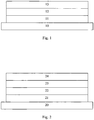
- an organic solar cell comprises at least a substrate 10, an anode 11, a light absorbing unit 12, and a cathode 13.
- the stack of layers can also be inverted, wherein layer 11 would be the cathode, and layer 13 would be the anode. Additional light absorbing units can be provided in the organic solar cell.
- the substrate 10 can be a transparent substrate, such as a glass, or polymeric plate or web.
- the anode 11 can be a transparent conducting oxide, such as ITO, FTO, AlZO.
- the cathode 13 can comprise aluminum or an aluminum alloy.
- At least one light absorbing unit 12 can comprise a blend of a thiophene containing a polymer and a compound according to Formula 1.
- the light absorbing unit 12 can comprise a blend of a donor polymer, preferentially a thiophene containing a polymer, and an acceptor, preferentially a fullerene or a soluble fullerene derivative.
- a layer comprising the compound according to Formula 1 (such as a doped electron transport layer) or consisting of it (such as an electron extracting layer) is formed between the light absorbing unit 12 and the cathode 13.
- the layer structure can be inverted.
- the anode 11 is not transparent and mainly comprises aluminum or an aluminum alloy.
- the substrate 10 is not necessarily transparent.
- the cathode 13 comprises a transparent conducting oxide layer or a thin transparent metal layer having a thickness of less than 30 nm.
- the substrate 10, the anode 11, and the cathode 13 are transparent.
- the overall device is semi-transparent, because it does not have 100% absorption of the incident light for any wavelength in the visible range of wavelengths.
- stacked devices e.g. tandem devices
- at least one additional light absorbing unit is formed between the light absorbing unit 12 and the cathode 13.
- Additional organic or inorganic layers may be formed to provide a suitable electronic connection and optical optimization of the layer position.
- at least parts of these functions are provided by layers comprising a compound according to the Formula 1.
- Fig.2 shows a stack of layers representing an organic solar cell comprising a substrate 20, an anode 21, a light absorbing unit 22 comprising an absorption layer, an organic electron transport layer (ETL) 23, and a cathode 24.
- the stack of layers can also be inverted.
- the ETL can be formed between the cathode 24 and the absorption layer 22. Additional light absorbing units can be provided in the solar cell.
- the organic electron transport layer 23 can comprise as its main component an electron transport material (ETM) as a matrix material and the compound according to the Formula 1 as a dopant.
- ETM electron transport material
- the ETL 23 can have any thickness. Its thickness is preferably smaller than 40 nm in the case that there is no additional absorption layer between the light absorbing layer 22 and the cathode 24.
- All figures are schematic representations of the layered structure of a solar cell. Some device features are not shown such as electrical connections, encapsulation, optical structures which are external to the electrodes, etc.
- the layer thicknesses are not drawn to scale. At least one of the electrodes (anode and/or cathode) is transparent in the wavelength range in which the device is active.
- the light absorbing unit 22 is a donor-acceptor bulk heterojunction, e.g. a blend of donor-acceptor materials.
- the donor is preferentially formed by a strong absorbing compound comprising a pyrrole or a thiophene group.
- the acceptor is preferentially a C 58 , C 60 , or C 70 fullerene or a soluble fullerene derivative.
- the ETL 23 can comprise a compound according to the Formula 1 as a dopant.
- the light absorbing unit 22 is a donor-acceptor bulk heterojunction e.g. a blend of donor-acceptor materials.
- the donor is preferentially formed by a strong absorbing compound comprising a pyrrole or a thiophene group.
- the acceptor can be a compound according to Formula 1.
- the precipitate was filtered, dried, suspended in 2 M sodium hydroxide solution and stirred for 5 minutes at 45°C. 5 g (7.5 mmol; 49 %) brown solid was obtained after filtration, washing with water and drying in vacuo.
- the product was purified by gradient sublimation for analytical characterisation.
- the precipitate was filtered, dried, suspended in 2 M sodium hydroxide solution and stirred for 5 minutes at 45°C. 1.2 g (2.4 mmol; 26 %) brown solid was obtained after filtration, washing with water and drying in vacuo.
- the product was purified by gradient sublimation for analytical characterisation.
- C60 doped with 10mol% of compound 1 showed a conductivity of 1.3 S/cm.
- C60 doped with 10mol% of compound 4 showed a conductivity of 4.6 S/cm.
- C60 doped with 10mol% of compound 2 showed a conductivity of 2.1E-2 S/cm.
- C60 doped with 10mol% of compound 28 showed a conductivity of 2.1E-2 S/cm.
- C60 doped with 10mol% of compound 29 showed a conductivity of 0.35 S/cm.
- C60 was used as a standard reference and it is clear that other electron transport materials with similar electronic transport properties can also be doped.
- a pn junction device was used to benchmark the new dopants according to Formula 1 with the strong donor Tetrakis (1,3,4,6,7,8 - Hexahydro - 2H - pyrimido [1,2-a] pyrimidinato) ditungsten (II) (W(hpp)4).
- the pn-junction device was made on a glass substrate using ITO as anode, a 50 nm p-doped HTL (hole transport layer), a 50 nm C60 layer doped with one of the new dopants according to Formula 1 as ETL (electron transport layer), and an Al cathode.
- the voltage necessary for a current density of 5 mA/cm 2 was 0.09 V for compound 1, 0.12 V for compound 2, and 0.03 V for compound 4. These values are surprisingly good given the much lower donating strength than W(hpp)4 (HOMO ⁇ -1.0 V vs Fc), which in a comparative example required a voltage of 0.01 V for the same current density.
- a state of the art organic solar cell was fabricated with the following procedure.
- a patterned glass substrate coated with ITO was cleaned with standard procedure.
- the substrate was loaded into the vacuum trough a glove box with nitrogen.
- the organic layers were deposited with conventional VTE (vacuum thermal evaporation).
- VTE vacuum thermal evaporation
- First a 40 nm thick 15 .% (molar) p-doped N4,N4,N4",N4"-tetra([1,1'-biphenyl]-4-yl)-[1,1':4',1"-terphenyl]-4,4"-diamine (HT1) layer was deposited through a shadow mask over the ITO.
- a 10 nm undoped Boron subphthalocyanine chloride (SubPc) layer was deposited over the doped HT1.
- a 25 nm undoped C60 layer followed.
- a 15 nm thick C60 layer doped (10 wt.%) with the strong n-dopant W(hpp)4 was deposited on top of the undoped C60 layer.
- Device 3 An organic solar cell can be made with the same layer structure as device 2 except that compound 4 was used instead of W(hpp)4. Under identical conditions, the device typically shows increased performance with a short circuit current of 4.93 mA/cm 2 , a FF of 54.9 % and an open circuit voltage of 1.08 V with an overall power efficiency of 2.91%.
- the IxV curves of the device with and without illumination are shown in Fig. 3 .
- Tandem organic solar cells comprising the new compound according to Formula 1 as dopants show higher power conversion efficiency than a comparative device, which were identical except for the n-dopant (W(hpp)4). Power conversion efficiency up to 3.9% could be achieved, while the best comparative tandem solar cell had 3.7%.
Description
- The invention relates to an electronic device.
- Organic solar cells (OSCs), also known as organic photovoltaic (OPV) devices, have the most different device architectures. Typically, they comprise at least one organic semiconducting layer that is arranged between two electrodes. The organic layer can be a blend of a donor and an acceptor such as P3HT (poly3-hexyl-tiophene) and PCBM (phenyl C61 Butyric Acid Methyl Ester). Such simple device structures only achieve reasonably efficiencies if interfacial injection layers are used to facilitate charge carrier injection/extraction (Liao et al., Appl. Phys. Lett., 2008.92: p. 173303). Other organic solar cells have multi-layer structures, sometimes even hybrid polymer and small molecule structures. Also tandem or multi-unit stacks are known (see
US 2007/090371 A1 , or Ameri, et al., Energy & Env. Science, 2009.2: p. 347). Multi-layer devices can be easier optimized since different layers can comprise different chemical compounds (or simply compounds) and their mixtures which are suitable for different functions. Typical functional layers are transport layers, photoactive layers, injection layers, etc. - Optically active compounds are compounds with a high absorption coefficient, for at least a certain wavelength range of the solar spectra, which compounds convert absorbed photons into excitons which excitons in turn contribute to the photocurrent. The photoactive compounds are typically used in a donor-acceptor heterojunction, where at least one of the donor or the acceptor is the light absorbing compound. The interface of the donor-acceptor heterojunction is responsible for separating the generated excitons into charge carriers. The heterojunction can be a bulk-heterojunction (a blend), or a flat (also called planar) heterojunction, additional layers can also be provided (Hong et al, J. Appl. Phys., 2009.106: p. 064511).
- The loss by recombination must be minimized for high efficiency OPV devices. Therefore, the compounds in the heterojunction must have high charge carrier mobilities and high exciton diffusion lengths. The excitons have to be separated into charge carriers at the heterointerface and the charge carriers have to leave the optically active region before any recombination takes place. For that reasons, currently, fullerenes (C60, C70, PCBM, and so on) are the preferred choice as acceptor materials in OPV devices.
- Transport compounds for opto-electronic devices are required to be transparent, at least in the wavelengths wherein the device is active, and have good semiconducting properties. These semiconducting properties are intrinsic, such as energy levels or mobility, or extrinsic, such as charge carrier density. The charge carrier density can also be extrinsically influenced by doping the compound with an electrical dopant.
- OSCs very often require the use of at least one n-dopant in an n-doped electron transport layer, or as a pure interlayer promoting electron injection from a conductive layer into a semiconductor or from a semiconductor into another semiconductor.
- Several different n-dopants are known, such as Tetrakis(1,3,4,6,7,8-Hexahydro-2H-pyrimido [1,2-a]pyrimidinato)ditungsten (II) from
EP 1 768 200 B1 , Bis(2,2'-terpyridin)ruthenium, and others. One main problem of n-dopants is that since they are strong donors, they easily degrade by reacting with atmospheric oxygen. There are not many known compounds which are able to directly work as n-dopants which are also air stable. Precursor-compounds were developed with the aim to provide air stable organic compounds and being able to work as n-dopants, examples of such precursors are disclosed inWO 2007/107306 A1 . - Also, only a few organic compounds are known to be able to efficiently dope low LUMO compounds used in OSCs, such as fullerenes (e.g. C60) or fullerene derivatives (e.g. PCBM), for example the compounds disclosed in
US 2007/145355 A1 . - Guidi et al., The Journal of Organic Chemistry, 2005, 70, 7737, discloses bis(phosphine imide)s and the use thereof as organic electron donors.
- Escobar et al., Organic Letters, 2002, 4, 2213, discloses electron-donating properties of p-phenylene phospine imides.
- Matni et al., Magnetic Resonance in Chemistry, 2007, 45, 1011 discloses ESR/DFT studies of bis-iminophosphorane cation radicals.
- Matni et al., Chemical Physics letters, 2005, 411, 23, discloses oxidation products of iminophosphorane and bis-iminophosphorane.
-
US 3,188,294 A discloses phosphonium salts, polymers prepared therefrom and a process of making the same. - Pomerantz et al., Journal of Organic Chemistry, 1986, 51, 1223, discloses cyclic voltammetry of N-aryl-P,P,P-triphenylphospha-λ5-azenes.
- It is the object of the invention to provide improved technologies for an electronic device. Other objectives are to provide high conductivities and thermal stabilities of doped layers in electronic devices. Another objective not forming part of the present invention is to provide a compound with an easy processability.
- The object is solved by the electronic device according to the independent claim 1. Advantageous embodiments are subject matter of the dependent claims.
- According to one aspect of the invention an electronic device comprising an n-dopand according to formula 1
A-B (1),
wherein

- Ar1 is a C6-C18 arylene, which can be monocyclic or polycyclic and may be optionally substituted by one or more C1-C10-alkyl or C3-C10-cycloalkyl groups,
- Ar2 is a C6-C18 arene skeleton, optionally substituted with electron donating groups R4,
- B1 and B2 are independently selected from B and Ar2,
- B3 is independently selected from the same group as B
- R1, R2, R3 are independently selected from alkyl, arylalkyl, cycloalkyl, aryl, dialkylamino,
- x is selected from 0, 1, 2 and 3, wherein for x > 1 each Ar1 may be different,
- y is a non-zero integer up to the overall count of valence sites on the arene skeleton,
- z is a integer from zero up to the overall count of valence sites on the arene skeleton minus y Preferably,
- Ar2 is a benzene or naphthalene skeleton,
- R4 is selected from alkyl and alkoxy,
- R1, R2, R3 are independently selected from alkyl, arylalkyl, cycloalkyl, aryl, dialkylamino,
- x = 0 or Ar1 = phenylene,
- y is selected from 1, 2, 3 and 4 if Ar2 is benzene2 or from 1, 2, 3, 4, 5 and 6 if Ar2 is naphthalene,
- z is selected from 0 and 1 if Ar2 is benzene or from 0, 1 and 2 if Ar2 is naphthalene.
- According to another preferred aspect of the invention, in the compound according to the Formula 1
- Ar2 is a benzene skeleton
- R4 is selected from alkyl and alkoxy,
- R1, R2, R3 are independently selected from alkyl, arylalkyl, cycloalkyl, aryl, dialkylamino,
- x = 0 or Ar1 = 1,4-phenylene,
- y is selected from 1, 2, 3 and 4.
- According to yet other preferred embodiments of the invention, in the compound according to Formula 1,
- R4 is selected from alkyl and alkoxy,
- R1, R2, R3 are independently selected from alkyl, arylalkyl, cycloalkyl, aryl, dialkylamino,
- x=0
- A = H,, y = 1 or 2, z = 1 or
- A = B3 and the sum of all y is at least 3.
- The components R1 - R4 and the superscripts x, y and z of the compound according to Formula 1 can be selected independently from each other for each B. Also in the case that A equals B leading to a compound B-B3, the B and B3 can be different. The component A of the compound according to Formula 1 can be arranged in para position, ortho position or meta position at any of the phenyl rings.
- In any of the above mentioned embodiments of the invention, preferably, R1-R3 is straight or branched, saturated or unsaturated C1-C24 alkyl, saturated or unsaturated C3-C24 cycloalkyl or alkyl comprising at least one cyclic structure, wherein up to four ether linkages can be included within any of the above mentioned alkyl or cycloalkyl structure with a provision that oxygen atoms are in any case separated by at least two carbon atoms, C6-C24 aryl, wherein the overall count of carbon atoms includes also any possible substitution by a single substituent or more substituents selected from saturated or unsaturated, straight or branched alkyl or cycloalkyl, aryl, arylalkyl or alkylaryl groups and within this substitution up to three alkyl groups can be attached to the arene core by an ether linkage or up to six alkyl groups can be attached through a disubstituted nitrogen atom, C7-C25 arylalkyl, wherein the overall C atom count includes also a possible substitution on the arene ring or rings and within this substitution up to three alkyl groups can be attached to the arene ring or rings through an ether linkage or up to six alkyl groups through a disubstituted nitrogen atom, C2-C24 dialkylamino, wherein the alkyl groups may be the same or different, straight or branched, may include also alicyclic or aromatic structures or be unsaturated with a provision that the carbon atom bearing a double or triple bond is not adjacent to nitrogen. The two alkyls in the dialkylamino group may be so linked that they form a cycle comprising the nitrogen atom. Up to four ether linkages can be included between methylene groups of the dialkylamino group, with a provision that in any case the nitrogen and/or oxygen atoms are separated by at least two carbon atoms. Two R1-R3 groups may be linked so that they form a cyclic structure including the phosphorus atom. More preferably, R1-R3 is a C1-C4 alkyl, C3-C10 cycloalkyl, C7-C10 arylalkyl, C6-C14 aryl, C2-C12 dialkylamino. Particularly preferably, each of R1-R3 is independently selected from methyl, isopropyl, tert.-butyl, cyclohexyl, phenyl, tolyl, xylyl, mesityl, naphthyl, anthryl, phenanthryl, 1,1'-biphenyl-yl, 1,3-diisopropylphenyl, benzyl, 4-methoxybenzyl, dimethylamino. Most preferably, R1-R3 is 1,3-dimethylphenyl.
- If R4 is alkyl or alkoxy, then the alkyl group can be straight or branched, saturated or unsaturated. That alkyl can also include a cyclic structure, saturated or unsaturated. If more than one R4 occur on the same arene skeleton, then they also can form together a cyclic structure. Preferably, if R4 is alkyl or alkoxy, its overall count of carbon atoms is in the range C1-C22. More preferably, R4 is selected from methyl, methoxy, ethyl, ethoxy, propyl, propoxy, isopropyl, isopropoxy, butyl, butoxy, tert-butyl, tert.-butoxy, cyclohexyl, benzyl, benzyloxy.
- In a preferred embodiment, the electronic device is an organic electronic device.
- According to a preferred embodiment, the electronic device has a layered structure comprising several layers, wherein at least one of the layers comprises the compound of Formula 1. The electronic device may further comprise an electron transport layer. Alternatively or supplementary, the electronic device may comprise a first electrode and / or a second electrode.
- In a preferred embodiment, the layer of the electronic device comprising the compound of Formula 1 is an electron transport layer. More preferably, the electronic device comprises an electron transport layer which comprises an electron transport compound and the compound according to Formula 1 forming a homogeneous mixture. According to a another preferred mode of the invention, the layer of the electronic device comprising the compound of Formula 1 is in direct contact to an electron transport layer. In a preferred mode of the invention, the electron transport layer comprises a fullerene or a fullerene derivative as its main component.
- If used as an electron extracting layer, the layer of the electronic device comprising the compound of Formula 1 has preferably a thickness of less than 5 nm.
- Preferably, the layer of the electronic device comprising the compound of Formula 1 is in direct contact to an electrode, more preferably a cathode. In addition or alternatively, the layer comprising the compound according to Formula 1 is arranged between the electron transport layer and the cathode.
- In one aspect of the invention, the electronic device comprises a connecting unit. In a preferred embodiment, the layer of the electronic device comprising the compound of Formula 1 is part of the connecting unit.
- In a preferred mode of the invention, the electronic device is a solar cell, preferably an organic solar cell (OSC). The solar cell can comprise, for example, an anode, a cathode and a light absorbing layer. In a preferred embodiment, the organic solar cell further comprises the compound according to Formula 1, wherein the compound is comprised between the light absorbing layer and the cathode. In a preferred aspect of the invention, the organic solar cell comprises a pi, ni, or pin structure, comprising a first p, i, or n layer each. Here, p denotes a p-doped hole transport layer, n denotes a n-doped electron transport layer, and i is an intrinsic photoactive layer (see
US 2007/090371 A1 for further details). The transport layers have a greater HOMO-LUMO gap than the photoactive layer (HOMO - highest occupied molecular orbital, LUMO - lowest unoccupied molecular orbital). - The solar cell can preferentially comprise a light absorbing unit comprising the light absorbing layer and an additional light absorbing unit comprising an additional light absorbing layer. The connecting unit can be a pn-junction connecting the light absorbing unit to the additional light absorbing unit. Preferably, the connecting unit is a pn-junction connecting the light absorbing unit to the additional light absorbing unit in a tandem device or in a multiple stacked device. Multiple stacked devices are devices with three or more light absorbing units, sometimes also called multi tandem. Multiple stacked pin, pi, or ni devices are preferred. In addition or in alternative, the connecting unit can be a pn-junction connecting the cathode or the anode to the light absorbing unit.
- The invention has the advantages that high conductivity can be achieved by doping typical electron transport materials (ETM) used for OSCs. With the use of the compound according to Formula 1, it is possible to obtain conductivities on the order of 1 S/cm with a doping concentration of 10 mol.%, which is a high value for organic systems. Furthermore, the compound according to Formula 1 has a high stability allowing it to be processed, for example, in vacuum, e.g. by vacuum thermal evaporation (VTE), or by organic vapor phase deposition (OVPD). Alternatively, the compound according to Formula 1 can be processed by solution processing under inert atmosphere or even exposed to air.
- The compound according to Formula 1 is inserted in a matrix material forming a doped layer. Herewith, cations derived from the molecules of the compound according to Formula 1 are formed, in particular by the transfer of at least one electron from the compound according to Formula 1 to the surrounding matrix material. In the process, anions of the matrix material are also formed. In this way, the matrix material obtains a conductivity which is increased in comparison to the conductivity of the undoped matrix material.
- The conductivity of an undoped matrix material is generally approximately 10-8 S/cm, in particular often around 10-10 S/cm. The matrix material should have a sufficiently high purity. Such purity can be achieved using conventional methods, for example gradient sublimation. By doping, the conductivity of the matrix material can be increased to more than 10-6 S/cm. This applies in particular to a matrix material which has a reduction potential of less than -0.3 V vs. Fc/Fc+, preferably less than -0.8 V vs. Fc/Fc+. The notation Fc/Fc+ relates to the redox pair ferrocene/ferrocenium, which is used as reference in an electrochemical potential determination, for example by cyclic voltammetry. Details of cyclovoltammetry and other methods to determine reduction potentials and the relation of the ferrocene/ferrocenium reference couple to various reference electrodes can be found in A. J. Bard et al., "Electrochemical Methods: Fundamentals and Applications", Wiley, 2. Edition, 2000. For typical electron transport materials in OSC, the reduction potential is around -0.8 V vs. Fc/Fc+.
- In the present application, a dopant is to be understood as a material which is mixed in a matrix material ("the matrix material is doped with the dopant"). It is also common in the state of the art to use the term "electrical dopant", or just "n-dopant" for the dopant for an ETM.
- The layer of the electronic device comprising the compound of Formula 1 arranged adjacent to the electron transport layer can be used in an OSC as an electron extracting layer. It was found that the compound according to Formula 1 can be used as an electron injection layer in an electronic component, preferably between an electrode and a semiconductor layer which may be doped. Alternatively or supplementary, the compound according to Formula 1 can be used as a blocking layer, preferably between an absorbing layer and a transport layer, or as a semiconductor layer in electronic components.
- In one preferred aspect of the invention, all organic layers of the electronic device are constituted from small molecules. Preferentially, the small molecules can be deposited by VTE (vacuum thermal evaporation).
- In another aspect of the invention, at least one organic semiconducting layer comprises a polymer, wherein the polymer layer and / or at least one additional semiconducting layer comprise a compound according to Formula 1.
- The compounds according to Formula 1 have a special advantage of forming very stable n-doped layers with a relatively high conductivity.
- The synthesis of the compound according to Formula 1 is known from the literature, see for instance, Horner and Oediger, "Phosphororganische Verbindungen, XVIII: Phosphinimino-Verbindungen aus Phosphindihalogeniden und Primaren Aminen", Liebigs Annalen der Chemie 1959, v. 627, pp. 132-162.
- In the following, exemplary embodiments are disclosed with reference to figures of a drawing. The figures show:
- Fig. 1
- is a schematic diagram representing a stack of layers which forms a solar cell.
- Fig. 2
- is a schematic diagram representing a stack of layers of a solar cell comprising an electron transport layer (ETL).
- Fig. 3
- shows the IxV (current versus voltage) curves of a solar cell with and without illumination.
- According to
Fig. 1 , an organic solar cell comprises at least asubstrate 10, ananode 11, alight absorbing unit 12, and acathode 13. The stack of layers can also be inverted, whereinlayer 11 would be the cathode, andlayer 13 would be the anode. Additional light absorbing units can be provided in the organic solar cell. - In one embodiment, the
substrate 10 can be a transparent substrate, such as a glass, or polymeric plate or web. Theanode 11 can be a transparent conducting oxide, such as ITO, FTO, AlZO. Thecathode 13 can comprise aluminum or an aluminum alloy. At least onelight absorbing unit 12 can comprise a blend of a thiophene containing a polymer and a compound according to Formula 1. Alternatively, thelight absorbing unit 12 can comprise a blend of a donor polymer, preferentially a thiophene containing a polymer, and an acceptor, preferentially a fullerene or a soluble fullerene derivative. In this embodiment, a layer comprising the compound according to Formula 1 (such as a doped electron transport layer) or consisting of it (such as an electron extracting layer) is formed between the light absorbingunit 12 and thecathode 13. Optionally, the layer structure can be inverted. - In an alternative embodiment, the
anode 11 is not transparent and mainly comprises aluminum or an aluminum alloy. Thesubstrate 10 is not necessarily transparent. Thecathode 13 comprises a transparent conducting oxide layer or a thin transparent metal layer having a thickness of less than 30 nm. - Still in connection to
Fig.1 , in another embodiment, thesubstrate 10, theanode 11, and thecathode 13 are transparent. In this embodiment, the overall device is semi-transparent, because it does not have 100% absorption of the incident light for any wavelength in the visible range of wavelengths. - Multiple stacked devices (e.g. tandem devices) can also be provided. In such devices, at least one additional light absorbing unit is formed between the light absorbing
unit 12 and thecathode 13. Additional organic or inorganic layers may be formed to provide a suitable electronic connection and optical optimization of the layer position. Preferentially, at least parts of these functions are provided by layers comprising a compound according to the Formula 1. -
Fig.2 shows a stack of layers representing an organic solar cell comprising asubstrate 20, ananode 21, a light absorbing unit 22 comprising an absorption layer, an organic electron transport layer (ETL) 23, and acathode 24. The stack of layers can also be inverted. The ETL can be formed between thecathode 24 and the absorption layer 22. Additional light absorbing units can be provided in the solar cell. - In one embodiment, the organic electron transport layer 23 can comprise as its main component an electron transport material (ETM) as a matrix material and the compound according to the Formula 1 as a dopant. The ETL 23 can have any thickness. Its thickness is preferably smaller than 40 nm in the case that there is no additional absorption layer between the light absorbing layer 22 and the
cathode 24. - All embodiments as described in connection to
Fig. 1 can also be applied for the solar cell according toFig. 2 . - All figures are schematic representations of the layered structure of a solar cell. Some device features are not shown such as electrical connections, encapsulation, optical structures which are external to the electrodes, etc. The layer thicknesses are not drawn to scale. At least one of the electrodes (anode and/or cathode) is transparent in the wavelength range in which the device is active.
- In another embodiment, the light absorbing unit 22 is a donor-acceptor bulk heterojunction, e.g. a blend of donor-acceptor materials. The donor is preferentially formed by a strong absorbing compound comprising a pyrrole or a thiophene group. The acceptor is preferentially a C58, C60, or C70 fullerene or a soluble fullerene derivative. The ETL 23 can comprise a compound according to the Formula 1 as a dopant.
- In still another embodiment, the light absorbing unit 22 is a donor-acceptor bulk heterojunction e.g. a blend of donor-acceptor materials. The donor is preferentially formed by a strong absorbing compound comprising a pyrrole or a thiophene group. The acceptor can be a compound according to Formula 1.
- In the following table, preferred exemplary compounds according to Formula 1 are listed.
compound number 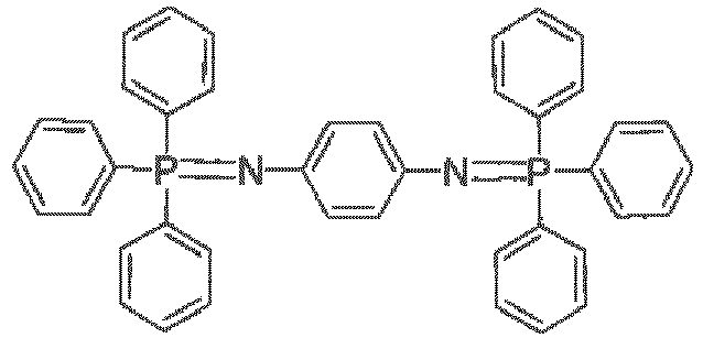
1 
2 
3 
4 
5 
6 
7 
8 
9 
10 
11 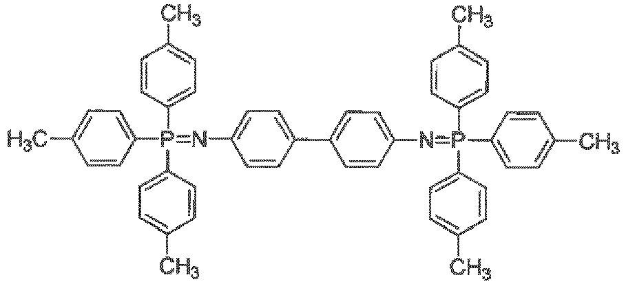
12 
13 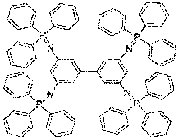
14 
15 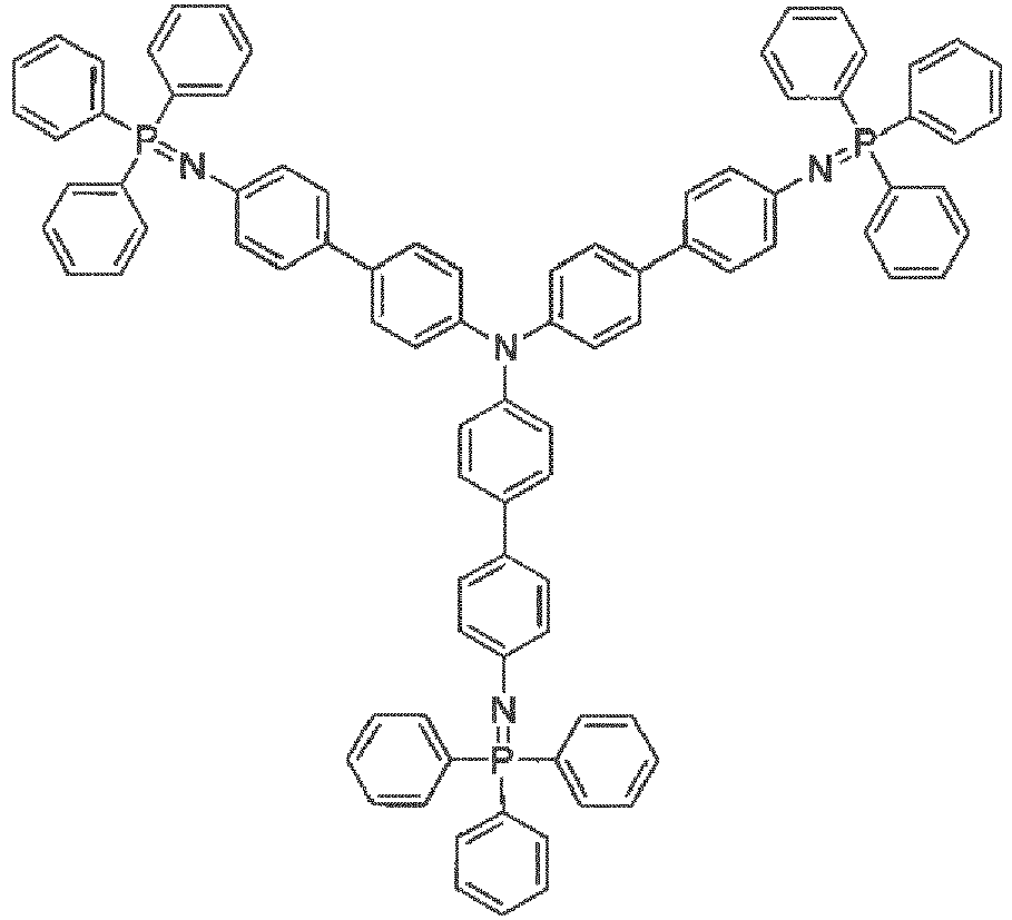
16 
17 
18 
19 
20 
21 
22 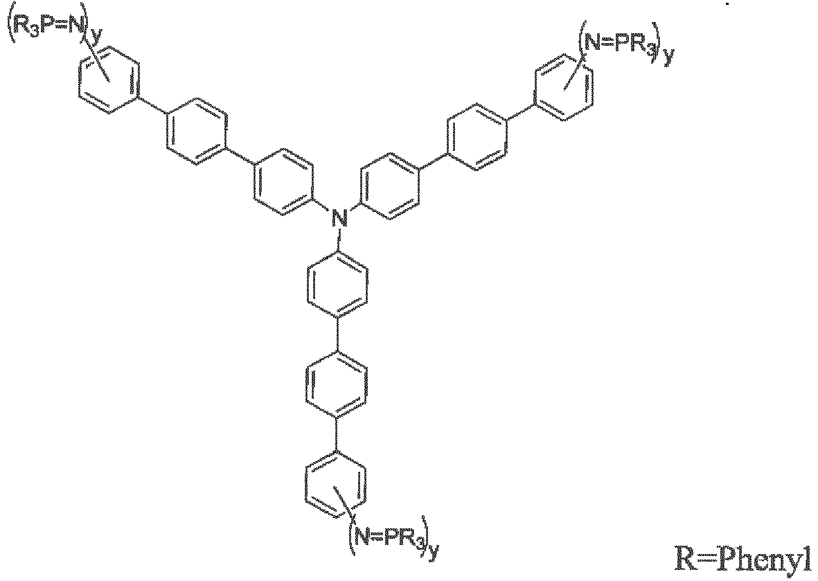
23 
24 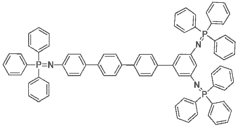
25 
26 
27 
28 
29 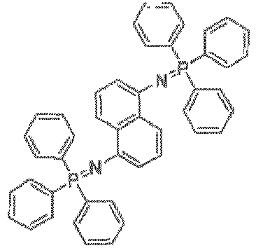
30 
31 - In the following, further details of some exemplary compounds according to Formula 1 are provided.
- 12.3 g (37.0 mmol) triphenylphosphine dichloride were dissolved in 80 ml benzene. 10 ml triethylamine and 2.0 g (18.5 mmol) 1,4-phenylene diamine were added and the mixture was heated for 2 days under reflux. After cooling, the suspension was filtered and the residue was washed first with diluted sodium hydroxide solution and then with ethanol/water. 9.20 g (14.6 mmol; 79%) yellow solid was obtained after drying in vacuum. The product was purified by gradient sublimation for analytical characterisation.
- Melting point (DSC): 272 °C
- CV (DCM): -0.40 V vs. Fc (rev)
- 10.0 g (30.0 mmol) triphenylphosphine dichloride was dissolved in 100 ml toluene. 8.5 ml triethylamine and 1.62 g (15.0 mmol) 1,2-phenylene diamine were added and the mixture was heated for 2 days at 95°C. After cooling, the suspension was filtered and the residue was washed with toluene. The residue was suspended in 2 M sodium hydroxide solution and stirred for 5 minutes at 45°C. 4.73 g (7.5 mmol; 50%) bright yellow solid were obtained after filtration and drying in vacuo. The product was purified by gradient sublimation for analytical characterisation.
- Melting point (DSC): 257 °C
- CV (DCM): -0.29 V vs. Fc
- 3.0 g (17.8 mmol) of 2-metboxy-4-nitroaniline and 0.8 g palladium on charcoal (10%) were added to 100 ml tetrahydrofurane. 8.7 ml (114.0 mmol) hydrazine monohydrate in 40 ml tetrahydrofuran were cautiously added and the reaction mixture was stirred at 90 °C for 3 hours. After cooling, the suspension was filtered and washed with tetrahydrofurane. The mother liquor was evaporated under reduced pressure to yield a gray residue. 2.44 g (17.7 mmol, 99%) product was stored under argon and used without further purification.
- 3.71 g (11.2 mmol) triphenylphosphine dichloride was dissolved in 50 ml toluene. A suspension of 3.1 ml (22.3 mmol) triethylamine and 0.77 g (5.6 mmol) 2-methoxy-1,4-phenylene diamine in 50 ml toluene was added and the mixture was heated for 2 days at 95 °C. After cooling, the suspension was filtered, the residue washed with toluene, suspended in a 2 M sodium hydroxide solution, stirred for 5 minutes at 45 °C, filtered and washed with water. 1.96 g (3.0 mmol; 53%) brown solid was obtained after filtration and drying in vacuum.
- Melting point (DSC): 206 °C
- CV (DCM): -0.45 V vs. Fc (rev)
- 11.70 g (49.3 mmol) hexachloroethane was added to a suspension of 15.0 g (49.3 mmol) tris(4-methylphenyl)phosphine in 80 ml acetonitrile under argon atmosphere. The mixture was stirred for 17 hours at 95 °C. After cooling, the solvent was removed under reduced pressure and the residue washed with toluene and hexane. 9.83 g (26.2 mmol; 53%) white solid were obtained after drying in high vacuum. The compound was used in the next transformation without further purification.
- A solution of 5.8 ml (41.6 mmol) triethylamine in 10 ml dry toluene was added under argon at 5 °C atmosphere to a mixture of 7.81 g (20.8 mmol) tris(4-methylphenyl)phosphine dichloride I in 80 ml dry toluene. 1.12 g (10.4 mmol) 1,4-phenylene diamine was added. The mixture was stirred at 110 °C for 1 hour. The yellow precipitate was filtered and washed with toluene and hexane. The dried crude product was suspended in 2 M sodium hydroxide solution and stirred for 5 minutes at 45 °C. 5.43 g (7.6 mmol; 73%) bright yellow solid was obtained after filtration, washing with water and drying in vacuo. The product was purified by gradient sublimation for analytical characterisation.
- Melting point (DSC): 267 °C
- CV (DCM): -0.46 V vs. Fc (rev)
- See above
- See above
- 2.0 g (5.3 mmol) tritoluylphosphine dichloride was dissolved in 10 ml toluene under argon. A suspension of 1.5 ml (10.7 mmol) triethylamine and 0.37 g (2.7 mmol) 2-methoxy-1,4-phenylene diamine in 15 ml toluene was added and the mixture was heated 18 hours at 90 °C. After cooling, the suspension was filtered, the residue washed with toluene,suspended in a 2 molar sodium hydroxide solution and stirred for 5 minutes at 45°C, filtered and washed with water. 0.43 g (0.6 mmol; 22%) yellow solid was obtained after filtration and drying in vacuo.
- Melting point (DSC): 239 °C
- CV (DCM): -0.51 V vs. Fc.
- 4.9 ml (35.2 mmol) triethylamine and 0.50 g (1.8 mmol) tetraaminobenzene tetrahydrochloride were suspended in 20 ml acetonitrile. 2.93 g (8.8 mmol) triphenylphosphine dichloride were dissolved in 15 ml acetonitrile and added to the suspension at 0 °C. The mixture was stirred at room temperature for 18 hours. The precipitate was filtered off, suspended in 2 molar sodium hydroxide solution and stirred for 5 minutes at 45 °C. 0.74 g (0.6 mmol; 35%) red brown solid was obtained after filtration and drying in vacuo.
- Melting point (DSC): 283 °C
- CV (DCM) = -1.02 V vs. Fc (rev.)
- 1.72 g (5.4 mmol) triphenylphosphine dichloride was dissolved in 8 ml dichloromethane under argon atmosphere. 1.8 ml (12.9 mmol) triethylamine in 2 ml dichloromethane was slowly added to the solution. 0.50 g (1.7 mmol) tris(4-aminophenyl)amine was added and the mixture was stirred at room temperature for 4 days. The reaction was diluted with dichloromethane and extracted with water. The organic phase was dried and the solvent removed under reduce pressure. The residue was suspended in 2 molar sodium hydroxide solution and stirred for 5 minutes at 45 °C. 1.50 g (1.4 mmol; 82%) solid was obtained after filtration and drying in vacuo.
- Melting point (DSC): 277 °C
- CV (DMF): -0.39 V vs. Fc.
- See above
- A solution of 3.8 ml (27.4 mmol) triethylamine in 10 ml dry toluene was added under argon atmosphere at 5 °C to a 3.82 g (10.2 mmol) tris(4-methylphenyl)phosphine dichloride dissolved in 40 ml toluene. 1.0 g (3.4 mmol) tris(4-aminophenyl)amine was added. The mixture was stirred at 110 °C for 1 hour. The precipitate was filtered and washed with toluene and hexane. The dried crude product was suspended in a 2 molar sodium hydroxide solution and stirred for 5 minutes at 45 °C. 3.06 g (2.6 mmol; 75%) pale yellow solid was obtained after filtration, washing with water and drying in vacuo.
- 4.15 g (12.5 mmol) triphenylphosphine dichloride was dissolved in 30 ml benzene. 3.4 ml triethylamine and 1.15 g (6.3 mmol) benzidine were added. The mixture was stirred under reflux for 3 hours. After cooling, the suspension was filtered and the yellow residue was washed first with diluted sodium hydroxide solution and then with ethanol/water. 3.20 g (4.7 mmol; 73%) yellow solid was obtained after drying in vacuo. The product was purified by gradient sublimation for analytical characterisation.
- Melting point (DSC): 283 °C
- CV (DCM): 0.0 V vs. Fc (rev.)
- 2.50 g (7.5 mmol) triphenylphosphine dichloride was dissolved in 50 ml toluene. 2.9 ml triethylamine and 0.88 g (3.4 mmol) 4,4"-diamino-p-terphenyl were added and the mixture was heated for 2 days at 95 °C. After cooling, the suspension was filtered and the residue was washed first with diluted sodium hydroxide solution and then with water and acetonitrile. 2.06 g (2.6 mmol; 78%) pale-yellow solid was obtained after drying in vacuum. The product was purified by gradient sublimation for analytical characterisation.
- Melting point (DSC): 322 °C
- CV (DCM): 0.22 V vs. Fc (rev)
- 11.7 g ((49.3 mmol) hexachloroethane was added to a suspension of 15.0 g (49.3 mmol) tris(4-methylphenyl)phosphine in 80 ml acetonitrile under argon atmosphere. The mixture was stirred for 17 hours at 95°C. After cooling, 200 ml dry toluene were added and 50 ml acetonitrile removed under reduced pressure. The precipitate was filtered and washed with 50 ml dry toluene and 50 ml dry hexane. 9.83 g (53%) white solid was obtained after drying in high vacuum.
- 1.69 g (4.5 mmol) in 3.3 ml dichloromethane was added to a solution of 0.52 g (2 mmol) tritolylphosphine dichloride in 5 ml toluene. After adding 1 g (10 mmol) triethylamine, the mixture was stirred at reflux for 3 hours. The precipitate was filtered, dried, suspended in 2 M sodium hydroxide solution and stirred for 5 minutes at 45°C. 0.93 g (1.1 mmol; 55 %) brown solid was obtained after filtration, washing with water and drying in vacuo. The product was purified by gradient sublimation for analytical characterisation.
- Melting point: 314°C
- CV (DCM): 0.18 V vs. Fc
- 0.63 g (9.3 mmol) sodium nitrite in 5 ml water and 0.56 g (9.3 mmol) urea in 5 ml water were added to a mixture of 1.2 g (4.5 mmol) [1,1':4',1"-terphenyl]-4,4"-diamine, 7.5 ml acetic acid and 3.3 ml sulphuric acid at 0°C. After stirring for 1 hour, 0.64 g (9.8 mmol) sodium azide in 5 ml water was added slowly. The mixture was stirred 3 hours at room temperature and poured on ice. The precipitate was filtrated, washed with water and dried in vacuo. The 1.3 g (4.2 mmol, 93%) brown solid was used without further purification.
- To a solution of 0.66 g (2.1 mmol) 4,4"-diazido-1,1':4',1"-terphenyl in 15 ml toluene, 1.48 g (4.2 mmol) tris(4-methoxyphenyl)phosphine in 5 ml toluene was added under argon atmosphere. After 18 hours stirring at room temperature, the solvent was distilled off and the residue washed with toluene. 1.70g (1.8 mmol) yellow powder was obtained after drying in vacuo.
- Melting point: 328°C
- Compound 28: N1,N4-bis(tricyclohexylphosphoranylidene)benzene-1,4-diamine
- 8.1 g ((34.2 mmol) hexachloroethane was added to a suspension of 9.6 g (34.2 mmol) tricyclohexylphosphine in 60 ml acetonitrile under argon atmosphere. The mixture was stirred for 16 hours at 95°C. After cooling to room temperature, a solution of 1.7 g (15.5 mmol) para-phenylene diamine and 11.5 ml (77.5 mmol) 2,3,4,6,7,8,9,10-octahydropyrimido[1,2-a]azepine in 25 ml acetonitrile was added. The mixture was stirred at 95°C for 16 hours and allowed to cool to room temperature. The precipitate was filtered, dried, suspended in 2 M sodium hydroxide solution and stirred for 5 minutes at 45°C. 5 g (7.5 mmol; 49 %) brown solid was obtained after filtration, washing with water and drying in vacuo. The product was purified by gradient sublimation for analytical characterisation.
- Melting point: 277°C
- CV (THF): -0.07 V vs. Fc
- 14.5 g ((61.0 mmol) hexachloroethane was added to a suspension of 10.0 g (61.0 mmol) tris(dimethylamino)phosphine in 75 ml acetonitrile under argon atmosphere. The mixture was stirred for 16 hours at 100°C. After cooling to room temperature, a solution of 3 g (27.7 mmol) para-phenylene diamine and 20.6 ml (138.5 mmol) 2,3,4,6,7,8,9,10-octahydropyrimido[l,2-a]azepine (1,8-diazobicyclo[5,4,0] undec-7-ene) in 15 ml acetonitrile was added. The mixture was stirred at 100°C for 16 hours and allowed to cool to room temperature. The solvent was distilled off up to 20 ml, the precipitate was filtrated, dried, suspended in 2 M sodium hydroxide solution and stirred for 5 minutes at 45°C. Extraction with toluene and washing with ethylacetate and drying in vacuo gave 1.2 g (2.8 mmol; 10 %) brown solid. The product was purified by gradient sublimation for analytical characterisation.
- Melting point: 127°C
- CV (DCM): -0.61 V vs. Fc
- 4.17 g (12.5 mmol) triphenylphosphine dichloride was dissolved in 30 ml benzene. 3.4 ml triethylamine and 1.0 g (6.25 mmol) naphthalene-1,5-diamine were added and the mixture was heated for 3 days at 80°C. After cooling, the suspension was filtered, the residue suspended in 2 M sodium hydroxide solution and stirred for 5 minutes at 45°C. 2.18 g (3.21 mmol; 51%) yellow solid was obtained after filtration and drying in vacuo. The product was purified by gradient sublimation for analytical characterisation.
- Melting point: 257°C
- CV (DCM): 0.26 V vs. Fc
- 4.7 g ((20 mmol) hexachloroethane was added to a suspension of 4 g (20 mmol) methyldiphenylphosphine in 25 ml acetonitrile under argon atmosphere. The mixture was stirred for 2.5 hours at 95°C. After cooling to room temperature, a solution of 0.98 g (9.1 mmol) para-phenylene diamine and 6.3 ml (45.5 mmol) 2,3,4,6,7,8,9,10-octahydropyrimido[1,2-a]azepine in 10 ml acetonitrile was added. The mixture was stirred at 95°C for 16 hours and allowed to cool to room temperature. The precipitate was filtered, dried, suspended in 2 M sodium hydroxide solution and stirred for 5 minutes at 45°C. 1.2 g (2.4 mmol; 26 %) brown solid was obtained after filtration, washing with water and drying in vacuo. The product was purified by gradient sublimation for analytical characterisation.
- Melting point: 225°C
- CV (DCM): -0.23 V vs. Fc
- The compounds proved to be effectively able to n-dope typical ETMs for OPVs. For example, C60 doped with 10mol% of compound 1 showed a conductivity of 1.3 S/cm. C60 doped with 10mol% of compound 4 showed a conductivity of 4.6 S/cm. C60 doped with 10mol% of compound 2 showed a conductivity of 2.1E-2 S/cm. C60 doped with 10mol% of compound 28 showed a conductivity of 2.1E-2 S/cm. C60 doped with 10mol% of compound 29 showed a conductivity of 0.35 S/cm. C60 was used as a standard reference and it is clear that other electron transport materials with similar electronic transport properties can also be doped. For example, 2,2',2"-(5H-diindeno[1,2-a:1',2'-c]fluorene-5,10,15-triylidene)trimalononitrile (ET1) doped with 10 mol.% of compounds 28 and 29, respectively, showed each a conductivity of more than 1E-4 S/cm which is sufficient, for instance, for OPV applications.
- Device 1: A pn junction device was used to benchmark the new dopants according to Formula 1 with the strong donor Tetrakis (1,3,4,6,7,8 - Hexahydro - 2H - pyrimido [1,2-a] pyrimidinato) ditungsten (II) (W(hpp)4). The pn-junction device was made on a glass substrate using ITO as anode, a 50 nm p-doped HTL (hole transport layer), a 50 nm C60 layer doped with one of the new dopants according to Formula 1 as ETL (electron transport layer), and an Al cathode. The voltage necessary for a current density of 5 mA/cm2 was 0.09 V for compound 1, 0.12 V for compound 2, and 0.03 V for compound 4. These values are surprisingly good given the much lower donating strength than W(hpp)4 (HOMO << -1.0 V vs Fc), which in a comparative example required a voltage of 0.01 V for the same current density.
- Device 2 (comparative): A state of the art organic solar cell was fabricated with the following procedure. A patterned glass substrate coated with ITO was cleaned with standard procedure. The substrate was loaded into the vacuum trough a glove box with nitrogen. In vacuum, the organic layers were deposited with conventional VTE (vacuum thermal evaporation). First a 40 nm thick 15 .% (molar) p-doped N4,N4,N4",N4"-tetra([1,1'-biphenyl]-4-yl)-[1,1':4',1"-terphenyl]-4,4"-diamine (HT1) layer was deposited through a shadow mask over the ITO. A 10 nm undoped Boron subphthalocyanine chloride (SubPc) layer was deposited over the doped HT1. A 25 nm undoped C60 layer followed. A 15 nm thick C60 layer doped (10 wt.%) with the strong n-dopant W(hpp)4 was deposited on top of the undoped C60 layer. An Al cathode was deposited on top. Under simulated solar spectra, the device showed the following parameters: Voc = 1.06 V, Jsc = 4.83 mA/cm2, FF = 52.5%, efficiency of 2.7 %.
- Device 3: An organic solar cell can be made with the same layer structure as device 2 except that compound 4 was used instead of W(hpp)4. Under identical conditions, the device typically shows increased performance with a short circuit current of 4.93 mA/cm2, a FF of 54.9 % and an open circuit voltage of 1.08 V with an overall power efficiency of 2.91%. The IxV curves of the device with and without illumination are shown in
Fig. 3 . - Tandem organic solar cells comprising the new compound according to Formula 1 as dopants show higher power conversion efficiency than a comparative device, which were identical except for the n-dopant (W(hpp)4). Power conversion efficiency up to 3.9% could be achieved, while the best comparative tandem solar cell had 3.7%. A replacement of C60 by ET1 in the 5 nm thick ETL of the pn junction, further improved the efficiency to 4.2%. That shows that the use of the new compound according to Formula 1 as dopant in electron transport layers which are connected to or part of a pn junction further improves organic electronic devices, especially organic solar cells.
- The features of the invention disclosed in the above specification, the claims and the drawing may be important individually as well as in any combination for the implementation of the invention in its various embodiments.
Claims (14)
- Electronic device comprising an n-dopand according to formula 1
A-B (1),
wherein

and wherein- Ar1 is a C6-C18 arylene, which can be monocyclic or polycyclic and may be optionally substituted by one or more C1-C10-alkyl or C3-C10-cycloalkyl groups,- Ar2 is a C6-C18 arene skeleton, optionally substituted with electron donating groups R4,- B1 and B2 are independently selected from B and Ar2,- B3 is independently selected from the same group as B- R1, R2, R3 are independently selected from alkyl, arylalkyl, cycloalkyl, aryl, dialkylamino,- x is selected from 0, 1, 2 and 3, wherein for x > 1 each Ar1 may be different,- y is a non-zero integer up to the overall count of valence sites on the arene skeleton,- z is a integer from zero up to the overall count of valence sites on the arene skeleton minus y. - Electronic device according to claim 1, wherein any of R1, R2, R3 is independently selected from
straight or branched, saturated or unsaturated C1-C24 alkyl,
saturated or unsaturated C3-C24 cycloalkyl or alkyl comprising at least one cyclic structure, wherein up to four ether linkages can be included within any of the above mentioned alkyl or cycloalkyl structure with a provision that oxygen atoms are in any case separated by at least two carbon atoms,
C6-C24 aryl, wherein the overall count of carbon atoms includes also any possible substitution by a single substituent or more substituents selected from saturated or unsaturated, straight or branched alkyl or cycloalkyl, aryl, arylalkyl or alkylaryl groups and within this substitution up to three alkyl groups can be attached to the arene core by an ether linkage or up to six alkyl groups can be attached through a disubstituted nitrogen atom,
C7-C25 arylalkyl, wherein the overall C atom count includes also a possible substitution on the arene ring or rings and within this substitution up to three alkyl groups can be attached to the arene ring or rings through an ether linkage or up to six alkyl groups through a disubstituted nitrogen atom,
C2-C24 dialkylamino, wherein the alkyl groups may be the same or different, straight or branched, may include also alicyclic or aromatic structures or be unsaturated with a provision that the carbon atom bearing a double or triple bond is not adjacent to nitrogen, the two alkyls in the dialkylamino group may be so linked that they form a cycle comprising the nitrogen atom and up to four ether linkages can be included between methylene groups of the dialkylamino group, and with a provision that in any case the nitrogen and/or oxygen atoms are separated by at least two carbon atoms,
or two groups selected from R1-R3 may be linked so that they form a cyclic structure including the phosphorus atom. - Electronic device according to claim 2, wherein any of R1, R2, R3 is independently selected from C1-C4 alkyl, C3-C10 cycloalkyl, C7-C10 arylalkyl, C6-C14 aryl, and C2-C12 dialkylamino.
- Electronic device according to any of claims 1-3, wherein each R4 is independently selected from alkyl and alkoxy, aryl and aryloxy having overall count of carbon atoms in the range C1-C22.
- Electronic device according to any of claims 1-4, wherein- Ar2 is a benzene or naphthalene skeleton,- Ar1 is phenylene, or x = 0- y is selected from 1, 2, 3 and 4 if Ar2 is benzene, or from 1, 2, 3, 4, 5 and 6 if Ar2 is naphthalene,- z is selected from 0 and 1 if Ar2 is benzene, or from 0, 1 and 2 if Ar2 is naphthalene.
- Electronic device according to claim 5, wherein- Ar2 is a benzene skeleton- Ar1 is 1,4-phenylene or x = 0.
- Electronic device according to any of claims 1-6, wherein each R4 is independently selected from methyl, methoxy, ethyl, ethoxy, propyl, propoxy, isopropyl, isopropoxy, butyl, butoxy, tert-butyl, tert.-butoxy, cyclohexyl, benzyl, and benzyloxy, or each of R1-R3 is independently selected from methyl, isopropyl, tert.-butyl, cyclohexyl, phenyl, tolyl, xylyl, mesityl, naphthyl, anthryl, phenanthryl, 1,1'-biphenyl-yl, 1,3-diisopropylphenyl, benzyl, 4-methoxybenzyl, and dimethylamino.
- Electronic device according to any of claims 1-7 having a layered structure comprising several layers.
- Electronic device according to claim 8, wherein the layer comprising the n-dopant of Formula 1 is an electron transport layer.
- Electronic device according to claim 8 or 9, wherein the layer comprising the n-dopant of Formula 1 has a thickness of less than 5 nm.
- Electronic device according to any of the claims 8 to 10, wherein the layer comprising the n-dopant of Formula 1 is in direct contact to an electrode, preferably a cathode.
- Electronic device according to any of the claims 8 to 11, wherein a layer comprising the n-dopant of Formula 1 is in direct contact to an electron transport layer.
- Electronic device according to any of the claims 8 to 12, wherein the layer comprising the n-dopant of Formula 1 is part of a connecting unit.
- Electronic device according to at least one of the preceding claims, wherein the device is a solar cell.
Priority Applications (3)
| Application Number | Priority Date | Filing Date | Title |
|---|---|---|---|
| EP23175436.7A EP4242216A3 (en) | 2011-06-22 | 2012-06-22 | Electronic device and compound |
| EP20155768.3A EP3667752A1 (en) | 2011-06-22 | 2012-06-22 | Electronic device and compound |
| EP12735779.6A EP2724388B1 (en) | 2011-06-22 | 2012-06-22 | Electronic device |
Applications Claiming Priority (3)
| Application Number | Priority Date | Filing Date | Title |
|---|---|---|---|
| EP11170945 | 2011-06-22 | ||
| PCT/EP2012/002647 WO2012175219A1 (en) | 2011-06-22 | 2012-06-22 | Electronic device and compound |
| EP12735779.6A EP2724388B1 (en) | 2011-06-22 | 2012-06-22 | Electronic device |
Related Child Applications (3)
| Application Number | Title | Priority Date | Filing Date |
|---|---|---|---|
| EP23175436.7A Division EP4242216A3 (en) | 2011-06-22 | 2012-06-22 | Electronic device and compound |
| EP20155768.3A Division-Into EP3667752A1 (en) | 2011-06-22 | 2012-06-22 | Electronic device and compound |
| EP20155768.3A Division EP3667752A1 (en) | 2011-06-22 | 2012-06-22 | Electronic device and compound |
Publications (2)
| Publication Number | Publication Date |
|---|---|
| EP2724388A1 EP2724388A1 (en) | 2014-04-30 |
| EP2724388B1 true EP2724388B1 (en) | 2020-03-11 |
Family
ID=46516665
Family Applications (3)
| Application Number | Title | Priority Date | Filing Date |
|---|---|---|---|
| EP23175436.7A Pending EP4242216A3 (en) | 2011-06-22 | 2012-06-22 | Electronic device and compound |
| EP20155768.3A Pending EP3667752A1 (en) | 2011-06-22 | 2012-06-22 | Electronic device and compound |
| EP12735779.6A Active EP2724388B1 (en) | 2011-06-22 | 2012-06-22 | Electronic device |
Family Applications Before (2)
| Application Number | Title | Priority Date | Filing Date |
|---|---|---|---|
| EP23175436.7A Pending EP4242216A3 (en) | 2011-06-22 | 2012-06-22 | Electronic device and compound |
| EP20155768.3A Pending EP3667752A1 (en) | 2011-06-22 | 2012-06-22 | Electronic device and compound |
Country Status (6)
| Country | Link |
|---|---|
| US (1) | US9502660B2 (en) |
| EP (3) | EP4242216A3 (en) |
| JP (4) | JP6461599B2 (en) |
| KR (1) | KR101971629B1 (en) |
| CN (1) | CN103765621B (en) |
| WO (1) | WO2012175219A1 (en) |
Cited By (1)
| Publication number | Priority date | Publication date | Assignee | Title |
|---|---|---|---|---|
| WO2024002424A1 (en) | 2022-06-29 | 2024-01-04 | Heliatek Gmbh | Organic electronic construction element with a chemical compound of general formula i, and use of such a chemical compound as n-dopant in an organic electronic construction element |
Families Citing this family (57)
| Publication number | Priority date | Publication date | Assignee | Title |
|---|---|---|---|---|
| EP2724389B1 (en) * | 2011-06-22 | 2018-05-16 | Novaled GmbH | Organic electronic device |
| KR102380808B1 (en) | 2013-12-06 | 2022-03-30 | 메르크 파텐트 게엠베하 | Substituted oxepines |
| KR102618668B1 (en) | 2013-12-19 | 2023-12-27 | 메르크 파텐트 게엠베하 | Heterocyclic spiro compounds |
| EP2963010B1 (en) | 2014-07-04 | 2018-02-21 | Novaled GmbH | Electronic device and compound |
| JP6695863B2 (en) | 2014-09-05 | 2020-05-20 | メルク パテント ゲーエムベーハー | Formulations and electronics |
| EP2999019B1 (en) * | 2014-09-19 | 2019-06-12 | Novaled GmbH | Organic light-emitting diode including an electron transport layer stack comprising different lithium compounds and elemental metal |
| WO2016107663A1 (en) | 2014-12-30 | 2016-07-07 | Merck Patent Gmbh | Formulations and electronic devices |
| DE102015200690A1 (en) | 2015-01-19 | 2016-07-21 | Siemens Aktiengesellschaft | Proazaphosphatrans as n-dopants in organic electronics |
| DE102015200699A1 (en) * | 2015-01-19 | 2016-07-21 | Siemens Aktiengesellschaft | Aminophosphazene bases as n-dopants in organic electronics |
| WO2016155866A1 (en) | 2015-03-30 | 2016-10-06 | Merck Patent Gmbh | Formulation of an organic functional material comprising a siloxane solvent |
| US10808170B2 (en) | 2015-06-12 | 2020-10-20 | Merck Patent Gmbh | Esters containing non-aromatic cycles as solvents for OLED formulations |
| US11046884B2 (en) | 2015-08-28 | 2021-06-29 | Merck Patent Gmbh | Formulation of an organic functional material comprising an epoxy group containing solvent |
| EP3147961A1 (en) | 2015-09-28 | 2017-03-29 | Novaled GmbH | Organic electroluminescent device |
| CN108368361A (en) | 2015-12-10 | 2018-08-03 | 默克专利有限公司 | Preparation containing the ketone comprising non-aromatic ring |
| CN108369997B (en) | 2015-12-15 | 2020-03-24 | 默克专利有限公司 | Aromatic group-containing esters as solvents for organic electronic formulations |
| EP3390549B1 (en) | 2015-12-16 | 2022-06-29 | Merck Patent GmbH | Formulations containing a solid solvent |
| EP3390550B1 (en) | 2015-12-16 | 2022-09-28 | Merck Patent GmbH | Formulations containing a mixture of at least two different solvents |
| EP3417033B1 (en) | 2016-02-17 | 2021-02-24 | Merck Patent GmbH | Formulation of an organic functional material |
| EP3208861A1 (en) | 2016-02-19 | 2017-08-23 | Novaled GmbH | Electron transport layer comprising a matrix compound mixture for an organic light-emitting diode (oled) |
| DE102016003104A1 (en) | 2016-03-15 | 2017-09-21 | Merck Patent Gmbh | Container comprising a formulation containing at least one organic semiconductor |
| EP3232490B1 (en) | 2016-04-12 | 2021-03-17 | Novaled GmbH | Organic light emitting diode comprising an organic semiconductor layer |
| ES2950397T3 (en) | 2016-05-04 | 2023-10-09 | Novaled Gmbh | Solar cell |
| JP2019523997A (en) | 2016-06-16 | 2019-08-29 | メルク パテント ゲーエムベーハー | Formulation of organic functional materials |
| CN109312183A (en) | 2016-06-17 | 2019-02-05 | 默克专利有限公司 | The preparation of organic functional material |
| TW201815998A (en) | 2016-06-28 | 2018-05-01 | 德商麥克專利有限公司 | Formulation of an organic functional material |
| CN109563402B (en) | 2016-08-04 | 2022-07-15 | 默克专利有限公司 | Preparation of organic functional materials |
| EP3312896B1 (en) * | 2016-10-24 | 2021-03-31 | Novaled GmbH | Organic electroluminescent device comprising a redox-doped electron transport layer and an auxiliary electron transport layer |
| EP3312899B1 (en) | 2016-10-24 | 2021-04-07 | Novaled GmbH | Electron transport layer stack for an organic light-emitting diode |
| JP7046938B2 (en) | 2016-10-31 | 2022-04-04 | メルク パテント ゲーエムベーハー | Formulation of organic functional materials |
| EP3532566B1 (en) | 2016-10-31 | 2021-04-21 | Merck Patent GmbH | Formulation of an organic functional material |
| US10892414B2 (en) | 2016-12-06 | 2021-01-12 | Merck Patent Gmbh | Process for making electronic device |
| WO2018108760A1 (en) | 2016-12-13 | 2018-06-21 | Merck Patent Gmbh | Formulation of an organic functional material |
| WO2018114883A1 (en) | 2016-12-22 | 2018-06-28 | Merck Patent Gmbh | Mixtures comprising at least two organofunctional compounds |
| TWI763772B (en) | 2017-01-30 | 2022-05-11 | 德商麥克專利有限公司 | Method for forming an organic element of an electronic device |
| TWI791481B (en) | 2017-01-30 | 2023-02-11 | 德商麥克專利有限公司 | Method for forming an organic electroluminescence (el) element |
| WO2018178136A1 (en) | 2017-03-31 | 2018-10-04 | Merck Patent Gmbh | Printing method for an organic light emitting diode (oled) |
| CN110494514A (en) | 2017-04-10 | 2019-11-22 | 默克专利有限公司 | The preparation of organic functional material |
| EP3609977A1 (en) | 2017-04-13 | 2020-02-19 | Merck Patent GmbH | Composition for organic electronic devices |
| JP7330898B2 (en) | 2017-05-03 | 2023-08-22 | メルク パテント ゲーエムベーハー | Formulation of organic functional material |
| EP3645766A1 (en) | 2017-06-26 | 2020-05-06 | Merck Patent GmbH | Homogeneous mixtures |
| US11591320B2 (en) | 2017-07-05 | 2023-02-28 | Merck Patent Gmbh | Composition for organic electronic devices |
| CN110832053A (en) | 2017-07-05 | 2020-02-21 | 默克专利有限公司 | Composition for organic electronic device |
| KR20200030573A (en) | 2017-07-18 | 2020-03-20 | 메르크 파텐트 게엠베하 | Formulation of organic functional materials |
| TWI785142B (en) | 2017-11-14 | 2022-12-01 | 德商麥克專利有限公司 | Composition for organic electronic devices |
| JP7293229B2 (en) | 2017-12-15 | 2023-06-19 | メルク パテント ゲーエムベーハー | Formulation of organic functional material |
| JP7247231B2 (en) | 2018-02-26 | 2023-03-28 | メルク パテント ゲーエムベーハー | Formulation of organic functional material |
| EP3802520A1 (en) | 2018-05-30 | 2021-04-14 | Merck Patent GmbH | Composition for organic electronic devices |
| CN112236488A (en) | 2018-06-15 | 2021-01-15 | 默克专利有限公司 | Preparation of organic functional material |
| EP3857621A1 (en) | 2018-09-24 | 2021-08-04 | Merck Patent GmbH | Method for the production of a granular material |
| JP2022506510A (en) | 2018-11-06 | 2022-01-17 | メルク パテント ゲーエムベーハー | How to Form Organic Devices for Electronic Devices |
| US20220127286A1 (en) | 2019-03-04 | 2022-04-28 | Merck Patent Gmbh | Ligands for nano-sized materials |
| JP2023522243A (en) | 2020-04-21 | 2023-05-29 | メルク パテント ゲーエムベーハー | Formulation of organic functional material |
| EP4169082A1 (en) | 2020-06-23 | 2023-04-26 | Merck Patent GmbH | Method for producing a mixture |
| WO2022122607A1 (en) | 2020-12-08 | 2022-06-16 | Merck Patent Gmbh | An ink system and a method for inkjet printing |
| KR20240000559A (en) | 2021-04-23 | 2024-01-02 | 메르크 파텐트 게엠베하 | Formulation of organic functional materials |
| KR20240012506A (en) | 2021-05-21 | 2024-01-29 | 메르크 파텐트 게엠베하 | Method for continuous purification of at least one functional substance and device for continuous purification of at least one functional substance |
| TW202349760A (en) | 2021-10-05 | 2023-12-16 | 德商麥克專利有限公司 | Method for forming an organic element of an electronic device |
Citations (5)
| Publication number | Priority date | Publication date | Assignee | Title |
|---|---|---|---|---|
| US3188294A (en) | 1960-03-17 | 1965-06-08 | Monsanto Co | Phosphonium salts, polymers prepared therefrom and processes of making same |
| JP2002014438A (en) | 2000-06-28 | 2002-01-18 | Fuji Photo Film Co Ltd | Heat developable photosensitive material |
| US20030170491A1 (en) | 2002-02-15 | 2003-09-11 | Eastman Kodak Company | Providing an organic electroluminescent device having stacked electroluminescent units |
| US20060014044A1 (en) | 2004-07-14 | 2006-01-19 | Au Optronics Corporation | Organic light-emitting display with multiple light-emitting modules |
| US20070145355A1 (en) | 2005-12-22 | 2007-06-28 | Ansgar Werner | Doped organic semiconductor material |
Family Cites Families (10)
| Publication number | Priority date | Publication date | Assignee | Title |
|---|---|---|---|---|
| GB9902697D0 (en) * | 1999-02-09 | 1999-03-31 | Bp Chem Int Ltd | Novel compounds |
| DE10143566A1 (en) * | 2001-09-05 | 2003-03-20 | Basf Ag | New 1,8-bis-imido-naphthalene compounds, useful as basic catalysts for chemical reactions |
| AU2004221377B2 (en) | 2003-03-19 | 2009-07-16 | Heliatek Gmbh | Photoactive component comprising organic layers |
| DE102004010954A1 (en) | 2004-03-03 | 2005-10-06 | Novaled Gmbh | Use of a metal complex as an n-dopant for an organic semiconductive matrix material, organic semiconductor material and electronic component |
| US7259405B2 (en) * | 2004-11-23 | 2007-08-21 | Au Optronics Corporation | Organic photoelectric device with improved electron transport efficiency |
| US20070046189A1 (en) * | 2005-08-31 | 2007-03-01 | Eastman Kodak Company | Intermediate connector for a tandem OLED device |
| EP1837927A1 (en) | 2006-03-22 | 2007-09-26 | Novaled AG | Use of heterocyclic radicals for doping of organic semiconductors |
| TW200838008A (en) * | 2006-12-04 | 2008-09-16 | Asahi Chemical Ind | Method for producing electronic device and coating solutions suitable for the production method |
| US8436345B2 (en) * | 2008-08-04 | 2013-05-07 | Pioneer Corporation | Organic electroluminescence device |
| JP5588631B2 (en) * | 2009-06-12 | 2014-09-10 | 帝人株式会社 | Resin composition containing cyclic carbodiimide |
-
2012
- 2012-06-22 KR KR1020147001830A patent/KR101971629B1/en active IP Right Grant
- 2012-06-22 US US14/126,331 patent/US9502660B2/en active Active
- 2012-06-22 EP EP23175436.7A patent/EP4242216A3/en active Pending
- 2012-06-22 EP EP20155768.3A patent/EP3667752A1/en active Pending
- 2012-06-22 WO PCT/EP2012/002647 patent/WO2012175219A1/en active Application Filing
- 2012-06-22 EP EP12735779.6A patent/EP2724388B1/en active Active
- 2012-06-22 JP JP2014516227A patent/JP6461599B2/en active Active
- 2012-06-22 CN CN201280031104.8A patent/CN103765621B/en active Active
-
2017
- 2017-05-31 JP JP2017108443A patent/JP2017206518A/en active Pending
-
2018
- 2018-09-03 JP JP2018164331A patent/JP2019006806A/en active Pending
-
2022
- 2022-05-31 JP JP2022088805A patent/JP2022116248A/en active Pending
Patent Citations (5)
| Publication number | Priority date | Publication date | Assignee | Title |
|---|---|---|---|---|
| US3188294A (en) | 1960-03-17 | 1965-06-08 | Monsanto Co | Phosphonium salts, polymers prepared therefrom and processes of making same |
| JP2002014438A (en) | 2000-06-28 | 2002-01-18 | Fuji Photo Film Co Ltd | Heat developable photosensitive material |
| US20030170491A1 (en) | 2002-02-15 | 2003-09-11 | Eastman Kodak Company | Providing an organic electroluminescent device having stacked electroluminescent units |
| US20060014044A1 (en) | 2004-07-14 | 2006-01-19 | Au Optronics Corporation | Organic light-emitting display with multiple light-emitting modules |
| US20070145355A1 (en) | 2005-12-22 | 2007-06-28 | Ansgar Werner | Doped organic semiconductor material |
Non-Patent Citations (10)
Cited By (2)
| Publication number | Priority date | Publication date | Assignee | Title |
|---|---|---|---|---|
| WO2024002424A1 (en) | 2022-06-29 | 2024-01-04 | Heliatek Gmbh | Organic electronic construction element with a chemical compound of general formula i, and use of such a chemical compound as n-dopant in an organic electronic construction element |
| DE102022116253A1 (en) | 2022-06-29 | 2024-01-04 | Heliatek Gmbh | Organic electronic component with a chemical compound of the general formula I, and use of such a chemical compound as an n-dopant in an organic electronic component |
Also Published As
| Publication number | Publication date |
|---|---|
| JP2022116248A (en) | 2022-08-09 |
| JP6461599B2 (en) | 2019-01-30 |
| JP2014524142A (en) | 2014-09-18 |
| US20140182681A1 (en) | 2014-07-03 |
| EP4242216A3 (en) | 2023-10-11 |
| KR20140053126A (en) | 2014-05-07 |
| WO2012175219A1 (en) | 2012-12-27 |
| KR101971629B1 (en) | 2019-04-23 |
| EP4242216A2 (en) | 2023-09-13 |
| CN103765621A (en) | 2014-04-30 |
| CN103765621B (en) | 2017-02-22 |
| US9502660B2 (en) | 2016-11-22 |
| EP2724388A1 (en) | 2014-04-30 |
| EP3667752A1 (en) | 2020-06-17 |
| JP2017206518A (en) | 2017-11-24 |
| JP2019006806A (en) | 2019-01-17 |
Similar Documents
| Publication | Publication Date | Title |
|---|---|---|
| EP2724388B1 (en) | Electronic device | |
| EP2614047B1 (en) | Compounds for organic photovoltaic devices | |
| CN104067400B (en) | Organic electronic device | |
| EP2962992B1 (en) | Fullerene derivative, organic solar cell using same, and manufacturing method thereof | |
| EP2828902B1 (en) | Inert solution-processable molecular chromophores for organic electronic devices | |
| EP2786434B1 (en) | Organic electronic device | |
| JP5417039B2 (en) | Indole derivatives and organic thin film solar cells using the same | |
| EP3287452B1 (en) | Heterocyclic compound and organic solar cell comprising same | |
| EP2718978A1 (en) | Compound for organic electronic device | |
| EP3648187B1 (en) | Perovskite solar cell | |
| KR102079941B1 (en) | spirobifluorene compound and perovskite solar cells comprising the same | |
| US10403824B2 (en) | Electronic device and compound | |
| JP2008166561A (en) | Material for photoelectric conversion element, and photoelectric conversion element using the same | |
| Mikie et al. | Spiro-1, 3-dioxolanofullerenes with low-lying LUMO level for organic solar cells | |
| US8933238B2 (en) | Aryloxy-phthalocyanines of group III metals | |
| KR101617843B1 (en) | fullerene derivative having spiro-bifluorenyl and organic electronic devices containing them |
Legal Events
| Date | Code | Title | Description |
|---|---|---|---|
| PUAI | Public reference made under article 153(3) epc to a published international application that has entered the european phase |
Free format text: ORIGINAL CODE: 0009012 |
|
| 17P | Request for examination filed |
Effective date: 20131216 |
|
| AK | Designated contracting states |
Kind code of ref document: A1 Designated state(s): AL AT BE BG CH CY CZ DE DK EE ES FI FR GB GR HR HU IE IS IT LI LT LU LV MC MK MT NL NO PL PT RO RS SE SI SK SM TR |
|
| DAX | Request for extension of the european patent (deleted) | ||
| 17Q | First examination report despatched |
Effective date: 20160718 |
|
| STAA | Information on the status of an ep patent application or granted ep patent |
Free format text: STATUS: EXAMINATION IS IN PROGRESS |
|
| RAP1 | Party data changed (applicant data changed or rights of an application transferred) |
Owner name: NOVALED GMBH |
|
| RAP1 | Party data changed (applicant data changed or rights of an application transferred) |
Owner name: NOVALED GMBH |
|
| REG | Reference to a national code |
Ref country code: DE Ref legal event code: R079 Ref document number: 602012068390 Country of ref document: DE Free format text: PREVIOUS MAIN CLASS: H01L0051000000 Ipc: H01L0051460000 |
|
| GRAP | Despatch of communication of intention to grant a patent |
Free format text: ORIGINAL CODE: EPIDOSNIGR1 |
|
| STAA | Information on the status of an ep patent application or granted ep patent |
Free format text: STATUS: GRANT OF PATENT IS INTENDED |
|
| RIC1 | Information provided on ipc code assigned before grant |
Ipc: H01L 27/30 20060101ALI20191001BHEP Ipc: C07F 9/06 20060101ALI20191001BHEP Ipc: C07F 9/535 20060101ALI20191001BHEP Ipc: H01L 51/46 20060101AFI20191001BHEP |
|
| INTG | Intention to grant announced |
Effective date: 20191016 |
|
| GRAS | Grant fee paid |
Free format text: ORIGINAL CODE: EPIDOSNIGR3 |
|
| GRAA | (expected) grant |
Free format text: ORIGINAL CODE: 0009210 |
|
| STAA | Information on the status of an ep patent application or granted ep patent |
Free format text: STATUS: THE PATENT HAS BEEN GRANTED |
|
| AK | Designated contracting states |
Kind code of ref document: B1 Designated state(s): AL AT BE BG CH CY CZ DE DK EE ES FI FR GB GR HR HU IE IS IT LI LT LU LV MC MK MT NL NO PL PT RO RS SE SI SK SM TR |
|
| REG | Reference to a national code |
Ref country code: GB Ref legal event code: FG4D |
|
| REG | Reference to a national code |
Ref country code: CH Ref legal event code: EP |
|
| REG | Reference to a national code |
Ref country code: AT Ref legal event code: REF Ref document number: 1244271 Country of ref document: AT Kind code of ref document: T Effective date: 20200315 |
|
| REG | Reference to a national code |
Ref country code: IE Ref legal event code: FG4D |
|
| REG | Reference to a national code |
Ref country code: DE Ref legal event code: R096 Ref document number: 602012068390 Country of ref document: DE |
|
| PG25 | Lapsed in a contracting state [announced via postgrant information from national office to epo] |
Ref country code: RS Free format text: LAPSE BECAUSE OF FAILURE TO SUBMIT A TRANSLATION OF THE DESCRIPTION OR TO PAY THE FEE WITHIN THE PRESCRIBED TIME-LIMIT Effective date: 20200311 Ref country code: FI Free format text: LAPSE BECAUSE OF FAILURE TO SUBMIT A TRANSLATION OF THE DESCRIPTION OR TO PAY THE FEE WITHIN THE PRESCRIBED TIME-LIMIT Effective date: 20200311 Ref country code: NO Free format text: LAPSE BECAUSE OF FAILURE TO SUBMIT A TRANSLATION OF THE DESCRIPTION OR TO PAY THE FEE WITHIN THE PRESCRIBED TIME-LIMIT Effective date: 20200611 |
|
| REG | Reference to a national code |
Ref country code: NL Ref legal event code: MP Effective date: 20200311 |
|
| PG25 | Lapsed in a contracting state [announced via postgrant information from national office to epo] |
Ref country code: BG Free format text: LAPSE BECAUSE OF FAILURE TO SUBMIT A TRANSLATION OF THE DESCRIPTION OR TO PAY THE FEE WITHIN THE PRESCRIBED TIME-LIMIT Effective date: 20200611 Ref country code: HR Free format text: LAPSE BECAUSE OF FAILURE TO SUBMIT A TRANSLATION OF THE DESCRIPTION OR TO PAY THE FEE WITHIN THE PRESCRIBED TIME-LIMIT Effective date: 20200311 Ref country code: SE Free format text: LAPSE BECAUSE OF FAILURE TO SUBMIT A TRANSLATION OF THE DESCRIPTION OR TO PAY THE FEE WITHIN THE PRESCRIBED TIME-LIMIT Effective date: 20200311 Ref country code: LV Free format text: LAPSE BECAUSE OF FAILURE TO SUBMIT A TRANSLATION OF THE DESCRIPTION OR TO PAY THE FEE WITHIN THE PRESCRIBED TIME-LIMIT Effective date: 20200311 Ref country code: GR Free format text: LAPSE BECAUSE OF FAILURE TO SUBMIT A TRANSLATION OF THE DESCRIPTION OR TO PAY THE FEE WITHIN THE PRESCRIBED TIME-LIMIT Effective date: 20200612 |
|
| REG | Reference to a national code |
Ref country code: LT Ref legal event code: MG4D |
|
| PG25 | Lapsed in a contracting state [announced via postgrant information from national office to epo] |
Ref country code: NL Free format text: LAPSE BECAUSE OF FAILURE TO SUBMIT A TRANSLATION OF THE DESCRIPTION OR TO PAY THE FEE WITHIN THE PRESCRIBED TIME-LIMIT Effective date: 20200311 |
|
| PG25 | Lapsed in a contracting state [announced via postgrant information from national office to epo] |
Ref country code: EE Free format text: LAPSE BECAUSE OF FAILURE TO SUBMIT A TRANSLATION OF THE DESCRIPTION OR TO PAY THE FEE WITHIN THE PRESCRIBED TIME-LIMIT Effective date: 20200311 Ref country code: SM Free format text: LAPSE BECAUSE OF FAILURE TO SUBMIT A TRANSLATION OF THE DESCRIPTION OR TO PAY THE FEE WITHIN THE PRESCRIBED TIME-LIMIT Effective date: 20200311 Ref country code: SK Free format text: LAPSE BECAUSE OF FAILURE TO SUBMIT A TRANSLATION OF THE DESCRIPTION OR TO PAY THE FEE WITHIN THE PRESCRIBED TIME-LIMIT Effective date: 20200311 Ref country code: IS Free format text: LAPSE BECAUSE OF FAILURE TO SUBMIT A TRANSLATION OF THE DESCRIPTION OR TO PAY THE FEE WITHIN THE PRESCRIBED TIME-LIMIT Effective date: 20200711 Ref country code: PT Free format text: LAPSE BECAUSE OF FAILURE TO SUBMIT A TRANSLATION OF THE DESCRIPTION OR TO PAY THE FEE WITHIN THE PRESCRIBED TIME-LIMIT Effective date: 20200805 Ref country code: RO Free format text: LAPSE BECAUSE OF FAILURE TO SUBMIT A TRANSLATION OF THE DESCRIPTION OR TO PAY THE FEE WITHIN THE PRESCRIBED TIME-LIMIT Effective date: 20200311 Ref country code: LT Free format text: LAPSE BECAUSE OF FAILURE TO SUBMIT A TRANSLATION OF THE DESCRIPTION OR TO PAY THE FEE WITHIN THE PRESCRIBED TIME-LIMIT Effective date: 20200311 Ref country code: CZ Free format text: LAPSE BECAUSE OF FAILURE TO SUBMIT A TRANSLATION OF THE DESCRIPTION OR TO PAY THE FEE WITHIN THE PRESCRIBED TIME-LIMIT Effective date: 20200311 |
|
| REG | Reference to a national code |
Ref country code: AT Ref legal event code: MK05 Ref document number: 1244271 Country of ref document: AT Kind code of ref document: T Effective date: 20200311 |
|
| REG | Reference to a national code |
Ref country code: DE Ref legal event code: R026 Ref document number: 602012068390 Country of ref document: DE |
|
| PLBI | Opposition filed |
Free format text: ORIGINAL CODE: 0009260 |
|
| PLAX | Notice of opposition and request to file observation + time limit sent |
Free format text: ORIGINAL CODE: EPIDOSNOBS2 |
|
| 26 | Opposition filed |
Opponent name: GLEISS GROSSE SCHRELL UND PARTNER MBB Effective date: 20201211 |
|
| PG25 | Lapsed in a contracting state [announced via postgrant information from national office to epo] |
Ref country code: IT Free format text: LAPSE BECAUSE OF FAILURE TO SUBMIT A TRANSLATION OF THE DESCRIPTION OR TO PAY THE FEE WITHIN THE PRESCRIBED TIME-LIMIT Effective date: 20200311 Ref country code: MC Free format text: LAPSE BECAUSE OF FAILURE TO SUBMIT A TRANSLATION OF THE DESCRIPTION OR TO PAY THE FEE WITHIN THE PRESCRIBED TIME-LIMIT Effective date: 20200311 Ref country code: DK Free format text: LAPSE BECAUSE OF FAILURE TO SUBMIT A TRANSLATION OF THE DESCRIPTION OR TO PAY THE FEE WITHIN THE PRESCRIBED TIME-LIMIT Effective date: 20200311 Ref country code: AT Free format text: LAPSE BECAUSE OF FAILURE TO SUBMIT A TRANSLATION OF THE DESCRIPTION OR TO PAY THE FEE WITHIN THE PRESCRIBED TIME-LIMIT Effective date: 20200311 Ref country code: ES Free format text: LAPSE BECAUSE OF FAILURE TO SUBMIT A TRANSLATION OF THE DESCRIPTION OR TO PAY THE FEE WITHIN THE PRESCRIBED TIME-LIMIT Effective date: 20200311 |
|
| REG | Reference to a national code |
Ref country code: CH Ref legal event code: PL |
|
| PG25 | Lapsed in a contracting state [announced via postgrant information from national office to epo] |
Ref country code: SI Free format text: LAPSE BECAUSE OF FAILURE TO SUBMIT A TRANSLATION OF THE DESCRIPTION OR TO PAY THE FEE WITHIN THE PRESCRIBED TIME-LIMIT Effective date: 20200311 Ref country code: PL Free format text: LAPSE BECAUSE OF FAILURE TO SUBMIT A TRANSLATION OF THE DESCRIPTION OR TO PAY THE FEE WITHIN THE PRESCRIBED TIME-LIMIT Effective date: 20200311 |
|
| PG25 | Lapsed in a contracting state [announced via postgrant information from national office to epo] |
Ref country code: LU Free format text: LAPSE BECAUSE OF NON-PAYMENT OF DUE FEES Effective date: 20200622 |
|
| REG | Reference to a national code |
Ref country code: BE Ref legal event code: MM Effective date: 20200630 |
|
| PG25 | Lapsed in a contracting state [announced via postgrant information from national office to epo] |
Ref country code: LI Free format text: LAPSE BECAUSE OF NON-PAYMENT OF DUE FEES Effective date: 20200630 Ref country code: IE Free format text: LAPSE BECAUSE OF NON-PAYMENT OF DUE FEES Effective date: 20200622 Ref country code: CH Free format text: LAPSE BECAUSE OF NON-PAYMENT OF DUE FEES Effective date: 20200630 |
|
| PLBB | Reply of patent proprietor to notice(s) of opposition received |
Free format text: ORIGINAL CODE: EPIDOSNOBS3 |
|
| PG25 | Lapsed in a contracting state [announced via postgrant information from national office to epo] |
Ref country code: BE Free format text: LAPSE BECAUSE OF NON-PAYMENT OF DUE FEES Effective date: 20200630 |
|
| PG25 | Lapsed in a contracting state [announced via postgrant information from national office to epo] |
Ref country code: TR Free format text: LAPSE BECAUSE OF FAILURE TO SUBMIT A TRANSLATION OF THE DESCRIPTION OR TO PAY THE FEE WITHIN THE PRESCRIBED TIME-LIMIT Effective date: 20200311 Ref country code: MT Free format text: LAPSE BECAUSE OF FAILURE TO SUBMIT A TRANSLATION OF THE DESCRIPTION OR TO PAY THE FEE WITHIN THE PRESCRIBED TIME-LIMIT Effective date: 20200311 Ref country code: CY Free format text: LAPSE BECAUSE OF FAILURE TO SUBMIT A TRANSLATION OF THE DESCRIPTION OR TO PAY THE FEE WITHIN THE PRESCRIBED TIME-LIMIT Effective date: 20200311 |
|
| PG25 | Lapsed in a contracting state [announced via postgrant information from national office to epo] |
Ref country code: MK Free format text: LAPSE BECAUSE OF FAILURE TO SUBMIT A TRANSLATION OF THE DESCRIPTION OR TO PAY THE FEE WITHIN THE PRESCRIBED TIME-LIMIT Effective date: 20200311 Ref country code: AL Free format text: LAPSE BECAUSE OF FAILURE TO SUBMIT A TRANSLATION OF THE DESCRIPTION OR TO PAY THE FEE WITHIN THE PRESCRIBED TIME-LIMIT Effective date: 20200311 |
|
| RDAF | Communication despatched that patent is revoked |
Free format text: ORIGINAL CODE: EPIDOSNREV1 |
|
| APBM | Appeal reference recorded |
Free format text: ORIGINAL CODE: EPIDOSNREFNO |
|
| APBP | Date of receipt of notice of appeal recorded |
Free format text: ORIGINAL CODE: EPIDOSNNOA2O |
|
| APAH | Appeal reference modified |
Free format text: ORIGINAL CODE: EPIDOSCREFNO |
|
| APBQ | Date of receipt of statement of grounds of appeal recorded |
Free format text: ORIGINAL CODE: EPIDOSNNOA3O |
|
| REG | Reference to a national code |
Ref country code: DE Ref legal event code: R079 Ref document number: 602012068390 Country of ref document: DE Free format text: PREVIOUS MAIN CLASS: H01L0051460000 Ipc: H10K0085000000 |
|
| P01 | Opt-out of the competence of the unified patent court (upc) registered |
Effective date: 20230515 |
|
| PGFP | Annual fee paid to national office [announced via postgrant information from national office to epo] |
Ref country code: FR Payment date: 20230510 Year of fee payment: 12 Ref country code: DE Payment date: 20230425 Year of fee payment: 12 |
|
| PGFP | Annual fee paid to national office [announced via postgrant information from national office to epo] |
Ref country code: GB Payment date: 20230504 Year of fee payment: 12 |