EP3131129B1 - Light-emitting element - Google Patents
Light-emitting element Download PDFInfo
- Publication number
- EP3131129B1 EP3131129B1 EP15776605.6A EP15776605A EP3131129B1 EP 3131129 B1 EP3131129 B1 EP 3131129B1 EP 15776605 A EP15776605 A EP 15776605A EP 3131129 B1 EP3131129 B1 EP 3131129B1
- Authority
- EP
- European Patent Office
- Prior art keywords
- layer
- semiconductor layer
- conductivity type
- type semiconductor
- light
- Prior art date
- Legal status (The legal status is an assumption and is not a legal conclusion. Google has not performed a legal analysis and makes no representation as to the accuracy of the status listed.)
- Active
Links
- 239000004065 semiconductor Substances 0.000 claims description 230
- 239000000463 material Substances 0.000 claims description 41
- 238000003892 spreading Methods 0.000 claims description 34
- 238000009413 insulation Methods 0.000 claims description 29
- 230000004888 barrier function Effects 0.000 claims description 28
- 229910002704 AlGaN Inorganic materials 0.000 claims description 22
- 238000009792 diffusion process Methods 0.000 claims description 18
- 230000000149 penetrating effect Effects 0.000 claims description 5
- 239000010410 layer Substances 0.000 description 491
- 239000000758 substrate Substances 0.000 description 47
- VYPSYNLAJGMNEJ-UHFFFAOYSA-N Silicium dioxide Chemical compound O=[Si]=O VYPSYNLAJGMNEJ-UHFFFAOYSA-N 0.000 description 24
- 239000011810 insulating material Substances 0.000 description 24
- GWEVSGVZZGPLCZ-UHFFFAOYSA-N Titan oxide Chemical compound O=[Ti]=O GWEVSGVZZGPLCZ-UHFFFAOYSA-N 0.000 description 22
- 229910052759 nickel Inorganic materials 0.000 description 18
- 238000000034 method Methods 0.000 description 17
- 229910001218 Gallium arsenide Inorganic materials 0.000 description 14
- 229910052737 gold Inorganic materials 0.000 description 14
- PNEYBMLMFCGWSK-UHFFFAOYSA-N aluminium oxide Inorganic materials [O-2].[O-2].[O-2].[Al+3].[Al+3] PNEYBMLMFCGWSK-UHFFFAOYSA-N 0.000 description 13
- 229910052593 corundum Inorganic materials 0.000 description 13
- 239000000203 mixture Substances 0.000 description 13
- 229910001845 yogo sapphire Inorganic materials 0.000 description 13
- XLOMVQKBTHCTTD-UHFFFAOYSA-N Zinc monoxide Chemical compound [Zn]=O XLOMVQKBTHCTTD-UHFFFAOYSA-N 0.000 description 12
- 150000001875 compounds Chemical class 0.000 description 12
- 239000002019 doping agent Substances 0.000 description 12
- 229910052763 palladium Inorganic materials 0.000 description 12
- 229910052697 platinum Inorganic materials 0.000 description 12
- 229910052709 silver Inorganic materials 0.000 description 12
- 229910020286 SiOxNy Inorganic materials 0.000 description 11
- 238000004519 manufacturing process Methods 0.000 description 11
- 238000002161 passivation Methods 0.000 description 11
- 229910000980 Aluminium gallium arsenide Inorganic materials 0.000 description 10
- 229910005540 GaP Inorganic materials 0.000 description 10
- 230000004907 flux Effects 0.000 description 10
- 229910052814 silicon oxide Inorganic materials 0.000 description 10
- 229910052725 zinc Inorganic materials 0.000 description 10
- 239000011701 zinc Substances 0.000 description 10
- 229910052751 metal Inorganic materials 0.000 description 9
- 239000002184 metal Substances 0.000 description 9
- 229910052581 Si3N4 Inorganic materials 0.000 description 8
- 229910052741 iridium Inorganic materials 0.000 description 8
- 230000008569 process Effects 0.000 description 8
- 239000002356 single layer Substances 0.000 description 8
- 229910052681 coesite Inorganic materials 0.000 description 7
- 229910052906 cristobalite Inorganic materials 0.000 description 7
- 150000004767 nitrides Chemical class 0.000 description 7
- 239000000377 silicon dioxide Substances 0.000 description 7
- 229910052682 stishovite Inorganic materials 0.000 description 7
- 229910052905 tridymite Inorganic materials 0.000 description 7
- 229910052782 aluminium Inorganic materials 0.000 description 6
- 229910052802 copper Inorganic materials 0.000 description 6
- 238000005530 etching Methods 0.000 description 6
- 238000000605 extraction Methods 0.000 description 6
- 229910052733 gallium Inorganic materials 0.000 description 6
- 229910052735 hafnium Inorganic materials 0.000 description 6
- 229910052738 indium Inorganic materials 0.000 description 6
- VRIVJOXICYMTAG-IYEMJOQQSA-L iron(ii) gluconate Chemical compound [Fe+2].OC[C@@H](O)[C@@H](O)[C@H](O)[C@@H](O)C([O-])=O.OC[C@@H](O)[C@@H](O)[C@H](O)[C@@H](O)C([O-])=O VRIVJOXICYMTAG-IYEMJOQQSA-L 0.000 description 6
- 238000000465 moulding Methods 0.000 description 6
- 230000003287 optical effect Effects 0.000 description 6
- 229910052710 silicon Inorganic materials 0.000 description 6
- 229910052718 tin Inorganic materials 0.000 description 6
- 229910052719 titanium Inorganic materials 0.000 description 6
- 238000001039 wet etching Methods 0.000 description 6
- 239000011787 zinc oxide Substances 0.000 description 6
- CIWBSHSKHKDKBQ-JLAZNSOCSA-N Ascorbic acid Chemical compound OC[C@H](O)[C@H]1OC(=O)C(O)=C1O CIWBSHSKHKDKBQ-JLAZNSOCSA-N 0.000 description 5
- 229910019897 RuOx Inorganic materials 0.000 description 4
- 229910045601 alloy Inorganic materials 0.000 description 4
- 239000000956 alloy Substances 0.000 description 4
- 229910052797 bismuth Inorganic materials 0.000 description 4
- 238000005229 chemical vapour deposition Methods 0.000 description 4
- 229910052804 chromium Inorganic materials 0.000 description 4
- 230000007423 decrease Effects 0.000 description 4
- 238000001312 dry etching Methods 0.000 description 4
- QZQVBEXLDFYHSR-UHFFFAOYSA-N gallium(III) oxide Inorganic materials O=[Ga]O[Ga]=O QZQVBEXLDFYHSR-UHFFFAOYSA-N 0.000 description 4
- 229910052732 germanium Inorganic materials 0.000 description 4
- 238000009616 inductively coupled plasma Methods 0.000 description 4
- 230000031700 light absorption Effects 0.000 description 4
- 229910052750 molybdenum Inorganic materials 0.000 description 4
- 230000000704 physical effect Effects 0.000 description 4
- 238000001020 plasma etching Methods 0.000 description 4
- 238000005498 polishing Methods 0.000 description 4
- 238000002310 reflectometry Methods 0.000 description 4
- 238000004544 sputter deposition Methods 0.000 description 4
- 229910052715 tantalum Inorganic materials 0.000 description 4
- -1 GZO Chemical compound 0.000 description 3
- 230000000052 comparative effect Effects 0.000 description 3
- 239000004020 conductor Substances 0.000 description 3
- 238000000151 deposition Methods 0.000 description 3
- JAONJTDQXUSBGG-UHFFFAOYSA-N dialuminum;dizinc;oxygen(2-) Chemical compound [O-2].[O-2].[O-2].[O-2].[O-2].[Al+3].[Al+3].[Zn+2].[Zn+2] JAONJTDQXUSBGG-UHFFFAOYSA-N 0.000 description 3
- 230000000694 effects Effects 0.000 description 3
- 238000002347 injection Methods 0.000 description 3
- 239000007924 injection Substances 0.000 description 3
- 239000003973 paint Substances 0.000 description 3
- 238000005240 physical vapour deposition Methods 0.000 description 3
- 239000000243 solution Substances 0.000 description 3
- SKRWFPLZQAAQSU-UHFFFAOYSA-N stibanylidynetin;hydrate Chemical compound O.[Sn].[Sb] SKRWFPLZQAAQSU-UHFFFAOYSA-N 0.000 description 3
- KEQXNNJHMWSZHK-UHFFFAOYSA-L 1,3,2,4$l^{2}-dioxathiaplumbetane 2,2-dioxide Chemical compound [Pb+2].[O-]S([O-])(=O)=O KEQXNNJHMWSZHK-UHFFFAOYSA-L 0.000 description 2
- 229910002601 GaN Inorganic materials 0.000 description 2
- GYHNNYVSQQEPJS-UHFFFAOYSA-N Gallium Chemical compound [Ga] GYHNNYVSQQEPJS-UHFFFAOYSA-N 0.000 description 2
- 239000004698 Polyethylene Substances 0.000 description 2
- 239000004743 Polypropylene Substances 0.000 description 2
- 229910000577 Silicon-germanium Inorganic materials 0.000 description 2
- 230000004308 accommodation Effects 0.000 description 2
- 230000007547 defect Effects 0.000 description 2
- 230000006866 deterioration Effects 0.000 description 2
- 238000010894 electron beam technology Methods 0.000 description 2
- 230000001747 exhibiting effect Effects 0.000 description 2
- APFVFJFRJDLVQX-UHFFFAOYSA-N indium atom Chemical compound [In] APFVFJFRJDLVQX-UHFFFAOYSA-N 0.000 description 2
- 230000001678 irradiating effect Effects 0.000 description 2
- 238000002955 isolation Methods 0.000 description 2
- 229910044991 metal oxide Inorganic materials 0.000 description 2
- 150000004706 metal oxides Chemical class 0.000 description 2
- 230000004048 modification Effects 0.000 description 2
- 238000012986 modification Methods 0.000 description 2
- 229910003465 moissanite Inorganic materials 0.000 description 2
- 238000007747 plating Methods 0.000 description 2
- 239000004417 polycarbonate Substances 0.000 description 2
- 229920000515 polycarbonate Polymers 0.000 description 2
- 229920000573 polyethylene Polymers 0.000 description 2
- 229920001155 polypropylene Polymers 0.000 description 2
- 239000002096 quantum dot Substances 0.000 description 2
- 230000009467 reduction Effects 0.000 description 2
- 229910052703 rhodium Inorganic materials 0.000 description 2
- 229910052594 sapphire Inorganic materials 0.000 description 2
- 239000010980 sapphire Substances 0.000 description 2
- 229910052711 selenium Inorganic materials 0.000 description 2
- 229910010271 silicon carbide Inorganic materials 0.000 description 2
- 229910000679 solder Inorganic materials 0.000 description 2
- 230000007480 spreading Effects 0.000 description 2
- 239000000126 substance Substances 0.000 description 2
- 230000003746 surface roughness Effects 0.000 description 2
- 229910052714 tellurium Inorganic materials 0.000 description 2
- 229910052721 tungsten Inorganic materials 0.000 description 2
- OAICVXFJPJFONN-UHFFFAOYSA-N Phosphorus Chemical compound [P] OAICVXFJPJFONN-UHFFFAOYSA-N 0.000 description 1
- DZLPZFLXRVRDAE-UHFFFAOYSA-N [O--].[O--].[O--].[O--].[Al+3].[Zn++].[In+3] Chemical compound [O--].[O--].[O--].[O--].[Al+3].[Zn++].[In+3] DZLPZFLXRVRDAE-UHFFFAOYSA-N 0.000 description 1
- 238000000071 blow moulding Methods 0.000 description 1
- 230000008859 change Effects 0.000 description 1
- 239000003086 colorant Substances 0.000 description 1
- 230000008878 coupling Effects 0.000 description 1
- 238000010168 coupling process Methods 0.000 description 1
- 238000005859 coupling reaction Methods 0.000 description 1
- 230000008021 deposition Effects 0.000 description 1
- YZZNJYQZJKSEER-UHFFFAOYSA-N gallium tin Chemical compound [Ga].[Sn] YZZNJYQZJKSEER-UHFFFAOYSA-N 0.000 description 1
- 239000011521 glass Substances 0.000 description 1
- AMGQUBHHOARCQH-UHFFFAOYSA-N indium;oxotin Chemical compound [In].[Sn]=O AMGQUBHHOARCQH-UHFFFAOYSA-N 0.000 description 1
- HRHKULZDDYWVBE-UHFFFAOYSA-N indium;oxozinc;tin Chemical compound [In].[Sn].[Zn]=O HRHKULZDDYWVBE-UHFFFAOYSA-N 0.000 description 1
- 239000007788 liquid Substances 0.000 description 1
- 239000007769 metal material Substances 0.000 description 1
- 230000000737 periodic effect Effects 0.000 description 1
- 239000004033 plastic Substances 0.000 description 1
- 229920003023 plastic Polymers 0.000 description 1
- 230000002265 prevention Effects 0.000 description 1
- 239000002210 silicon-based material Substances 0.000 description 1
- 229920003002 synthetic resin Polymers 0.000 description 1
- 239000000057 synthetic resin Substances 0.000 description 1
- 229910001887 tin oxide Inorganic materials 0.000 description 1
- YVTHLONGBIQYBO-UHFFFAOYSA-N zinc indium(3+) oxygen(2-) Chemical compound [O--].[Zn++].[In+3] YVTHLONGBIQYBO-UHFFFAOYSA-N 0.000 description 1
Images


Classifications
-
- H—ELECTRICITY
- H01—ELECTRIC ELEMENTS
- H01L—SEMICONDUCTOR DEVICES NOT COVERED BY CLASS H10
- H01L33/00—Semiconductor devices with at least one potential-jump barrier or surface barrier specially adapted for light emission; Processes or apparatus specially adapted for the manufacture or treatment thereof or of parts thereof; Details thereof
- H01L33/02—Semiconductor devices with at least one potential-jump barrier or surface barrier specially adapted for light emission; Processes or apparatus specially adapted for the manufacture or treatment thereof or of parts thereof; Details thereof characterised by the semiconductor bodies
- H01L33/08—Semiconductor devices with at least one potential-jump barrier or surface barrier specially adapted for light emission; Processes or apparatus specially adapted for the manufacture or treatment thereof or of parts thereof; Details thereof characterised by the semiconductor bodies with a plurality of light emitting regions, e.g. laterally discontinuous light emitting layer or photoluminescent region integrated within the semiconductor body
-
- H—ELECTRICITY
- H01—ELECTRIC ELEMENTS
- H01L—SEMICONDUCTOR DEVICES NOT COVERED BY CLASS H10
- H01L33/00—Semiconductor devices with at least one potential-jump barrier or surface barrier specially adapted for light emission; Processes or apparatus specially adapted for the manufacture or treatment thereof or of parts thereof; Details thereof
- H01L33/02—Semiconductor devices with at least one potential-jump barrier or surface barrier specially adapted for light emission; Processes or apparatus specially adapted for the manufacture or treatment thereof or of parts thereof; Details thereof characterised by the semiconductor bodies
- H01L33/04—Semiconductor devices with at least one potential-jump barrier or surface barrier specially adapted for light emission; Processes or apparatus specially adapted for the manufacture or treatment thereof or of parts thereof; Details thereof characterised by the semiconductor bodies with a quantum effect structure or superlattice, e.g. tunnel junction
-
- H—ELECTRICITY
- H01—ELECTRIC ELEMENTS
- H01L—SEMICONDUCTOR DEVICES NOT COVERED BY CLASS H10
- H01L21/00—Processes or apparatus adapted for the manufacture or treatment of semiconductor or solid state devices or of parts thereof
-
- H—ELECTRICITY
- H01—ELECTRIC ELEMENTS
- H01L—SEMICONDUCTOR DEVICES NOT COVERED BY CLASS H10
- H01L27/00—Devices consisting of a plurality of semiconductor or other solid-state components formed in or on a common substrate
- H01L27/15—Devices consisting of a plurality of semiconductor or other solid-state components formed in or on a common substrate including semiconductor components with at least one potential-jump barrier or surface barrier specially adapted for light emission
-
- H—ELECTRICITY
- H01—ELECTRIC ELEMENTS
- H01L—SEMICONDUCTOR DEVICES NOT COVERED BY CLASS H10
- H01L29/00—Semiconductor devices adapted for rectifying, amplifying, oscillating or switching, or capacitors or resistors with at least one potential-jump barrier or surface barrier, e.g. PN junction depletion layer or carrier concentration layer; Details of semiconductor bodies or of electrodes thereof ; Multistep manufacturing processes therefor
- H01L29/02—Semiconductor bodies ; Multistep manufacturing processes therefor
- H01L29/12—Semiconductor bodies ; Multistep manufacturing processes therefor characterised by the materials of which they are formed
- H01L29/18—Selenium or tellurium only, apart from doping materials or other impurities
-
- H—ELECTRICITY
- H01—ELECTRIC ELEMENTS
- H01L—SEMICONDUCTOR DEVICES NOT COVERED BY CLASS H10
- H01L29/00—Semiconductor devices adapted for rectifying, amplifying, oscillating or switching, or capacitors or resistors with at least one potential-jump barrier or surface barrier, e.g. PN junction depletion layer or carrier concentration layer; Details of semiconductor bodies or of electrodes thereof ; Multistep manufacturing processes therefor
- H01L29/66—Types of semiconductor device ; Multistep manufacturing processes therefor
- H01L29/68—Types of semiconductor device ; Multistep manufacturing processes therefor controllable by only the electric current supplied, or only the electric potential applied, to an electrode which does not carry the current to be rectified, amplified or switched
- H01L29/70—Bipolar devices
- H01L29/72—Transistor-type devices, i.e. able to continuously respond to applied control signals
-
- H—ELECTRICITY
- H01—ELECTRIC ELEMENTS
- H01L—SEMICONDUCTOR DEVICES NOT COVERED BY CLASS H10
- H01L33/00—Semiconductor devices with at least one potential-jump barrier or surface barrier specially adapted for light emission; Processes or apparatus specially adapted for the manufacture or treatment thereof or of parts thereof; Details thereof
- H01L33/02—Semiconductor devices with at least one potential-jump barrier or surface barrier specially adapted for light emission; Processes or apparatus specially adapted for the manufacture or treatment thereof or of parts thereof; Details thereof characterised by the semiconductor bodies
- H01L33/14—Semiconductor devices with at least one potential-jump barrier or surface barrier specially adapted for light emission; Processes or apparatus specially adapted for the manufacture or treatment thereof or of parts thereof; Details thereof characterised by the semiconductor bodies with a carrier transport control structure, e.g. highly-doped semiconductor layer or current-blocking structure
-
- H—ELECTRICITY
- H01—ELECTRIC ELEMENTS
- H01L—SEMICONDUCTOR DEVICES NOT COVERED BY CLASS H10
- H01L33/00—Semiconductor devices with at least one potential-jump barrier or surface barrier specially adapted for light emission; Processes or apparatus specially adapted for the manufacture or treatment thereof or of parts thereof; Details thereof
- H01L33/36—Semiconductor devices with at least one potential-jump barrier or surface barrier specially adapted for light emission; Processes or apparatus specially adapted for the manufacture or treatment thereof or of parts thereof; Details thereof characterised by the electrodes
- H01L33/38—Semiconductor devices with at least one potential-jump barrier or surface barrier specially adapted for light emission; Processes or apparatus specially adapted for the manufacture or treatment thereof or of parts thereof; Details thereof characterised by the electrodes with a particular shape
- H01L33/382—Semiconductor devices with at least one potential-jump barrier or surface barrier specially adapted for light emission; Processes or apparatus specially adapted for the manufacture or treatment thereof or of parts thereof; Details thereof characterised by the electrodes with a particular shape the electrode extending partially in or entirely through the semiconductor body
-
- H—ELECTRICITY
- H01—ELECTRIC ELEMENTS
- H01L—SEMICONDUCTOR DEVICES NOT COVERED BY CLASS H10
- H01L33/00—Semiconductor devices with at least one potential-jump barrier or surface barrier specially adapted for light emission; Processes or apparatus specially adapted for the manufacture or treatment thereof or of parts thereof; Details thereof
- H01L33/48—Semiconductor devices with at least one potential-jump barrier or surface barrier specially adapted for light emission; Processes or apparatus specially adapted for the manufacture or treatment thereof or of parts thereof; Details thereof characterised by the semiconductor body packages
- H01L33/62—Arrangements for conducting electric current to or from the semiconductor body, e.g. lead-frames, wire-bonds or solder balls
-
- H—ELECTRICITY
- H01—ELECTRIC ELEMENTS
- H01L—SEMICONDUCTOR DEVICES NOT COVERED BY CLASS H10
- H01L33/00—Semiconductor devices with at least one potential-jump barrier or surface barrier specially adapted for light emission; Processes or apparatus specially adapted for the manufacture or treatment thereof or of parts thereof; Details thereof
- H01L33/005—Processes
- H01L33/0093—Wafer bonding; Removal of the growth substrate
-
- H—ELECTRICITY
- H01—ELECTRIC ELEMENTS
- H01L—SEMICONDUCTOR DEVICES NOT COVERED BY CLASS H10
- H01L33/00—Semiconductor devices with at least one potential-jump barrier or surface barrier specially adapted for light emission; Processes or apparatus specially adapted for the manufacture or treatment thereof or of parts thereof; Details thereof
- H01L33/44—Semiconductor devices with at least one potential-jump barrier or surface barrier specially adapted for light emission; Processes or apparatus specially adapted for the manufacture or treatment thereof or of parts thereof; Details thereof characterised by the coatings, e.g. passivation layer or anti-reflective coating
- H01L33/46—Reflective coating, e.g. dielectric Bragg reflector
Definitions
- An embodiment relates to a light-emitting element.
- a light-emitting element is a p-n junction diode which converts electrical energy into light energy.
- the light-emitting element may be produced using compound semiconductors of groups III and V in the periodic table, and may implement various colors by adjusting a composition ratio of the compound semiconductors.
- the light-emitting element emits energy corresponding to a band-gap energy between a conduction band and a valence band when electrons of an n-type layer and holes of a p-type layer recombine upon application of a forward voltage. This energy is usually emitted in the form of heat or light. The light-emitting element emits the energy in the form of light.
- a nitride semiconductor has received much attention in development fields of optical devices and high-power electronic devices due to its high thermal stability and wide band-gap energy.
- a blue light-emitting element, a green light-emitting element, an ultraviolet (UV) light-emitting element, and the like using the nitride semiconductor have become commercialized and are widely used.
- An example of a light-emitting element according to the related art is a lateral-type light-emitting element in which an electrode layer is disposed in one direction of an epi-layer.
- an operating voltage (Vf) of the light-emitting element increases due to a narrow current flow, causing a reduction in current efficiency.
- Vf operating voltage
- a via hole-based vertical-type light-emitting element In order to solve such a problem, a via hole-based vertical-type light-emitting element has been developed.
- a via hole is formed below an epi-layer and an electrode is disposed therein.
- a plurality of mesa etching processes are performed for forming an n-contact, and an insulation layer is formed between the n-contact and a mesa etching hole.
- An embodiment provides a light-emitting element capable of improving luminous flux.
- a light-emitting element according to claims 1 to 6 is provided.
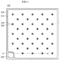
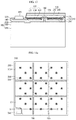
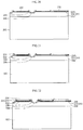
- Fig. 1 is a plan projection view of a light-emitting element 100 according to an embodiment of the invention
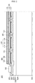
- Fig. 2 is an enlarged cross-sectional view taken along line A-A' of Fig. 1 .
- the light-emitting element 100 includes: a first conductivity type semiconductor layer 112; a second conductivity type semiconductor layer 116 disposed below the first conductivity type semiconductor layer 112; an active layer 114 disposed between the first conductivity type semiconductor layer 112 and the second conductivity type semiconductor layer 116; a plurality of holes H exposing parts of the first conductivity type semiconductor layer 112 to the bottom surface of the second conductivity type semiconductor layer 116 by penetrating the second conductivity type semiconductor layer 116 and the active layer 114; first contact electrodes 160 electrically connected to the first conductivity type semiconductor layer 112 from the bottom surface of the second conductivity type semiconductor layer 116 through the plurality of holes H; an insulation layer 140 disposed between the first contact electrodes 160 and the plurality of holes H; a first electrode layer 150 electrically connected to the first contact electrodes 160; and a second contact electrode 132 electrically connected to the second conductivity type semiconductor layer 116.
- the first electrode layer 150 may include a bonding layer 156 electrically connected to the first contact electrodes 160, and a support member 158 disposed below the bonding layer 156.
- the embodiment is directed to providing the light-emitting element capable of improving luminous flux.
- the embodiment includes a first current-spreading semiconductor layer 191 inside the first conductivity type semiconductor layer 112 above the first contact electrode 160.
- the first current-spreading semiconductor layer 191 includes a first conductive AlGaN/GaN superlattice layer or a first conductive AlGaN/GaN/InGaN superlattice layer.
- the first current-spreading semiconductor layer 191 made of n-AlGaN/GaN SLs or n-AlGaN/GaN/InGaN SLs is disposed above the first contact electrodes 160 formed in the via hole H, injected electrons flow while spreading in a lateral direction and the electrons are injected into an entire area of an active layer (MQW).
- MQW active layer
- the embodiment further includes a second current-spreading semiconductor layer 192 between the active layer 114 and the first conductivity type semiconductor layer 112.
- the first current-spreading semiconductor layer 191 and the second current-spreading semiconductor layer 192 may be collectively referred to as a current-spreading semiconductor layer 190.
- the second current-spreading semiconductor layer 192 is disposed to be lower than the first contact electrodes 160.
- the electrons injected by the first contact electrodes 160 or the electrons spread from the first current-spreading semiconductor layer 191 are additionally spread by arranging the second current-spreading semiconductor layer 192 between the active layer 114 and the first conductivity type semiconductor layer 112.
- carrier injection efficiency may be improved to increase luminous flux.
- a light-emitting element capable of improving luminous flux
- comparative examples can provide the method for producing the same, a light-emitting element package, and a lighting system.
- a light-emitting structure layer 110 may be formed above a growth substrate 105.
- the light-emitting structure layer 110 includes a first conductivity type semiconductor layer 112, an active layer 114, and a second conductivity type semiconductor layer 116.
- the embodiment includes a current-spreading semiconductor layer 190 for increasing luminous flux, and the current-spreading semiconductor layer 190 includes a first current-spreading semiconductor layer 191 and a second current-spreading semiconductor layer 192.
- the embodiment includes the first current-spreading semiconductor layer 191 formed inside the first conductivity type semiconductor layer 112.
- the first current-spreading semiconductor layer 191 includes a first conductive AlGaN/GaN superlattice layer or a first conductive AlGaN/GaN/InGaN superlattice layer.
- the first current-spreading semiconductor layer 191 made of n-AlGaN/GaN SLs or n-AlGaN/GaN/InGaN SLs is disposed above a first contact electrodes 160 to be formed later, injected electrons flow while spreading in a lateral direction and the electrons are injected into an entire area of an active layer (MQW).
- MQW active layer
- the embodiment further includes a second current-spreading semiconductor layer 192 between the active layer 114 and the first conductivity type semiconductor layer 112.
- the second current-spreading semiconductor layer 192 is disposed to be lower than the first contact electrodes 160 to be formed later.
- the electrons injected by the first contact electrodes 160 or the electrons spread from the first current-spreading semiconductor layer 191 are additionally spread by arranging the second current-spreading semiconductor layer 192 between the active layer 114 and the first conductivity type semiconductor layer 112.
- carrier injection efficiency may be improved to increase luminous flux.
- the embodiment it is possible to provide the light-emitting element capable of improving luminous flux.
- the first conductivity type semiconductor layer 112 includes a first semiconductor layer 112a of a first conductivity type above the growth substrate 105, and a first second semiconductor layer 112b of the first conductivity type formed after the first current-spreading semiconductor layer 101 is formed.
- the growth substrate 105 is loaded into a growth apparatus, and a layer or a pattern may be formed above the growth substrate 105 by using a compound semiconductor of group II to VI elements.
- the growth apparatus may employ an electron beam evaporator, a physical vapor deposition (PVD) apparatus, a chemical vapor deposition (CVD) apparatus, a plasma laser deposition (PLD) apparatus, a dual-type thermal evaporator, a sputtering apparatus, a metal organic chemical vapor deposition (MOCVD) apparatus, or the like, but is not limited to these apparatuses.
- PVD physical vapor deposition
- CVD chemical vapor deposition
- PLD plasma laser deposition
- MOCVD metal organic chemical vapor deposition
- the growth substrate 105 may be a conductive substrate or an insulating substrate.
- the growth substrate 105 may be selected from the group consisting of a sapphire substrate (Al 2 O 3 ), GaN, SiC, ZnO, Si, GaP, InP, Ga 2 O 3 , and GaAs.
- a buffer layer (not illustrated) may be formed above the growth substrate 105.
- the buffer layer reduces a difference of a lattice constant between the growth substrate 105 and a nitride semiconductor layer and may be made of a material selected from GaN, AlN, AlGaN, InGaN, InN, InAlGaN, AlInN, AlGaAs, GaP, GaAs, GaAsP, and AlGaInP.
- the undoped semiconductor layer may be formed above the buffer layer.
- the undoped semiconductor layer may be made of an undoped GaN-based semiconductor.
- the undoped semiconductor layer may be a semiconductor layer having lower conductivity than that of an n-type semiconductor layer.
- a first conductivity type semiconductor layer 112 is formed above the buffer layer or the undoped semiconductor layer.
- an active layer 114 is formed above the first conductivity type semiconductor layer 112, and a second conductivity type semiconductor layer 116 is sequentially stacked above the active layer 114.
- Another layer may be further disposed above or below each of the above-described semiconductor layers.
- a superlattice structure may be formed by using a group III-V compound semiconductor layer, but the present invention is not limited thereto.
- the first conductivity type semiconductor layer 112 may be selected from compound semiconductors of group III-V elements doped with a first conductive dopant, for example, GaN, AlN, AlGaN, InGaN, InN, InAlGaN, AlInN, AlGaAs, GaP, GaAs, GaAsP, and AlGaInP.
- the first conductivity type semiconductor layer 112 may be a semiconductor layer having an empirical formula of In x Al y Ga 1-x-y N (0 ⁇ x ⁇ 1, 0 ⁇ y ⁇ 1, 0 ⁇ x+y ⁇ 1).
- the first conductivity type semiconductor layer 112 may be an n-type semiconductor layer, and the first conductive dopant may include an n-type dopant such as Si, Ge, Sn, Se, and Te.
- the first conductivity type semiconductor layer 112 may be a single layer or a multi-layer, and may have a superlattice structure in which two different layers selected from GaN, AlN, AlGaN, InGaN, InN, InAlGaN, AlInN, AlGaAs, GaP, GaAs, GaAsP, and AlGaInP are alternately disposed.
- the active layer 114 may have a single quantum well structure, a multiple quantum well structure, a quantum wire structure, or a quantum dot structure.
- the active layer 114 may be formed by using a compound semiconductor material of group III-V elements in a cycle of a well layer and a barrier layer.
- the well layer may include a semiconductor layer having an empirical formula of In x Al y Ga 1-x-y N (0 ⁇ x ⁇ 1, 0 ⁇ y ⁇ 1, 0 ⁇ x+y ⁇ 1)
- the barrier layer may include a semiconductor layer having an empirical formula of In x Al y Ga 1-x-y N (0 ⁇ x ⁇ 1, 0 ⁇ y ⁇ 1, 0 ⁇ x+y ⁇ 1)
- the barrier layer may be made of a material having a higher band gap than that of the well layer.
- the active layer 114 may have at least one cycle selected from, for example, a cycle of InGaN well layer/GaN barrier layer, a cycle of InGaN well layer/AlGaN barrier layer, and a cycle of InGaN well layer/InGaN barrier layer.
- the second conductivity type semiconductor layer 116 may be formed above the active layer 114, and the second conductivity type semiconductor layer 116 may be selected from compound semiconductors of group III-V elements doped with a second conductive dopant, for example, GaN, AlN, AlGaN, InGaN, InN, InAlGaN, AlInN, AlGaAs, GaP, GaAs, GaAsP, and AlGaInP.
- the second conductivity type semiconductor layer 116 may be a semiconductor layer having an empirical formula of In x Al y Ga 1-x-y N (0 ⁇ x ⁇ 1, 0 ⁇ y ⁇ 1, 0 ⁇ x+y ⁇ 1).
- the second conductivity type semiconductor layer 116 may be a p-type semiconductor layer, and the second conductive dopant may include a p-type dopant such as Mg and Zn.
- the second conductivity type semiconductor layer 116 may be a single layer or a multi-layer, but is not limited thereto.
- the second conductivity type semiconductor layer 116 may have a superlattice structure in which two different layers selected from GaN, AlN, AlGaN, InGaN, InN, InAlGaN, AlInN, AlGaAs, GaP, GaAs, GaAsP, and AlGaInP are alternately disposed.
- the first conductivity type semiconductor layer 112, the active layer 114, and the second conductivity type semiconductor layer 116 may be defined as a light-emitting structure layer 110. Additionally, a third conductivity type semiconductor layer (not illustrated), for example, a semiconductor layer having an opposite polarity to the second conductivity type semiconductor layer, may be formed above the second conductivity type semiconductor layer 116.
- the light-emitting structure layer 110 may include at least one selected from an n-p junction structure, a p-n junction structure, an n-p-n junction structure, and a p-n-p junction structure.
- the second conductivity type semiconductor layer 116 is disposed on the uppermost layer of the light-emitting structure layer 110.
- a mesa etching process may be performed to remove a part of the light-emitting structure layer 110 and a part of the second current-spreading semiconductor layer 192.
- the plurality of holes H may form a predetermined angle from the first conductivity type semiconductor layer 112 to the top surface of the second conductivity type semiconductor layer 116, for example, an obtuse angle with respect to the top surface of the light-emitting structure layer 110.
- a horizontal width of the plurality of holes H may be gradually reduced downward.
- the horizontal width of the plurality of holes H may be gradually reduced upward.
- the removed regions of the active layer 114 and the first conductivity type semiconductor layer 112 may be reduced, contributing to luminous efficiency.
- a channel layer 120 may be formed above the plurality of holes H.
- the channel layer 120 may not be formed in a region where a first contact electrode 160 is to be formed. In this way, a part of the first conductivity type semiconductor layer 112 may be exposed.
- the channel layer 120 may function as an electrically insulating layer between the first contact electrode 160 to be formed, the active layer 114, and the second conductivity type semiconductor layer 116.
- the channel layer 120 may be made of one or more materials selected from SiO x , SiO x Ny, Al 2 O 3 , and TiO 2 .
- the reflectivity of the channel layer 120 may exceed 50%.
- the channel layer 120 may be made of an insulating material selected from SiO 2 , SiO x , SiO x N y , Si 3 N 4 , Al 2 O 3 , and TiO 2 , and may be made of a mixture of the insulating material and a light-reflecting material.
- the channel layer 120 may be made of a mixture of the insulating material and one or more materials selected from Ag, Ni, Al, Rh, Pd, Ir, Ru, Mg, Zn, Pt, Au, and Hf.
- the channel layer 120 when the emitted light travels downward, the channel layer 120 also reflects the light, thereby minimizing light absorption and increasing luminous efficiency.
- a second contact electrode 132 is formed above the second conductivity type semiconductor layer 116.
- the second contact electrode 132 ohmic-contacts the second conductivity type semiconductor layer 116.
- the second contact electrode 132 includes at least one conductive material and may be a single layer or a multi-layer.
- the second contact electrode 132 may include at least one of a metal, a metal oxide, and a metal nitride.
- the second contact electrode 132 may include a light-transmitting material.
- the second contact electrode 132 may include at least one of indium tin oxide (ITO), indium zinc oxide (IZO), IZO nitride (IZON), indium zinc tin oxide (IZTO), indium aluminum zinc oxide (IAZO), indium gallium zinc oxide (IGZO), indium gallium tin oxide (IGTO), aluminum zinc oxide (AZO), antimony tin oxide (ATO), gallium zinc oxide (GZO), IrO x , RuO x , RuO x /ITO, Ni/IrO x /Au, Ni/IrO x /Au/ITO, Pt, Ni, Au, Rh, and Pd.
- ITO indium tin oxide
- IZO indium zinc oxide
- IZON IZON
- IZTO indium aluminum zinc oxide
- IAZO indium gallium zinc oxide
- IGZO indium gallium zinc oxide
- a first contact electrode 160 is formed above the exposed first conductivity type semiconductor layer 112.
- the first contact electrode 160 may ohmic-contact the exposed first conductivity type semiconductor layer 112. When viewed from above, the first contact electrode 160 may have a circular or polygonal shape, but is not limited thereto.
- the top surface of the first contact electrode 160 is disposed between the top surface of the active layer 114 and the top surface of the first conductivity type semiconductor layer 112.
- the surface of the first conductivity type semiconductor layer 112, which contacts the first contact electrode 160, may be formed to have a flat structure as a Ga-face, but is not limited thereto.
- the width of the first contact electrode 160 may be gradually increased toward the top surface from the bottom surface.
- the width of the first contact electrode 160 may be gradually reduced toward the bottom surface from the top surface.
- a horizontal width of the bottom surface of the first contact electrode 160 matches a horizontal width of a diffusion barrier layer 154 contacting the first contact electrode 160.
- a reflection layer 134 may be formed above the second contact electrode 132.
- the reflection layer 134 may be disposed above the second contact electrode 132 and may reflect light incident through the second contact electrode 132.
- the reflection layer 134 may include a metal.
- the reflection layer 134 may be a single layer or a multi-layer made of a material selected from Ag, Ni, Al, Rh, Pd, Ir, Ru, Mg, Zn, Pt, Au, Hf, and an alloy of two or more of the listed materials.
- a capping layer 136 may be formed above the reflection layer 134.
- the second contact electrode 132, the reflection layer 134, and the capping layer 136 may be collectively referred to as a second electrode layer 130.
- the second electrode layer 130 may supply power from a pad electrode 180 to the second conductivity type semiconductor layer 116.
- the capping layer 136 may be disposed above the reflection layer 134 to supply the power from the pad electrode 180 to the reflection layer 134.
- the capping layer 136 may function as a current-spreading layer.
- the capping layer 136 may include a metal and may include at least one of Sn, Ga, In, Bi, Cu, Ni, Ag, Mo, Al, Au, Nb, W, Ti, Cr, Ta, Al, Pd, Pt, Si, and selective alloys thereof as a material having high conductivity.
- an insulation layer 140 is formed above the capping layer 136 and the channel layer 120.
- the insulation layer 140 may be formed to expose the first contact electrode 160.
- the insulation layer 140 electrically insulates the first contact electrode 160 from other semiconductor layers.
- the insulation layer 140 may be disposed between a first electrode layer 150 to be formed and the channel layer 120 to block electrical contact therebetween.
- the insulation layer 140 may be made of a material selected from SiO 2 , SiO x , SiO x N y , Si 3 N 4 , Al 2 O 3 , and TiO 2 .
- the reflectivity of the insulation layer 140 may exceed 50%.
- the insulation layer 140 may be made of an insulating material selected from SiO 2 , SiO x , SiO x N y , Si 3 N 4 , Al 2 O 3 , and TiO 2 , and may be made of a mixture of the insulating material and a light-reflecting material.
- the insulation layer 140 may be made of a mixture of the insulating material and one or more materials selected from Ag, Ni, Al, Rh, Pd, Ir, Ru, Mg, Zn, Pt, Au, and Hf.
- a physical property of the insulation layer 140 formed between the first contact electrode 160 and the plurality of holes H is formed by a reflection layer material, so that light absorption in the insulation layer 140 performing a passivation function is minimized, thereby increasing luminous efficiency.
- a diffusion barrier layer 154 may be formed above the insulation layer 140 and the first contact electrode 160, and a bonding layer 156 may be formed above the diffusion barrier layer 154
- the diffusion barrier layer 154 or the bonding layer 156 may include at least one of Ti, Au, Sn, Ni, Cr, Ga, In, Bi, Cu, Ag, and Ta.
- the diffusion barrier layer 154 or the bonding layer 156 may be formed by using at least one of a deposition method, a sputtering method, and a plating method, and may be attached with a conductive sheet.
- the bonding layer 156 may not be formed, but the present invention is not limited thereto.
- a support member 158 may be formed above the bonding layer 156.
- the diffusion barrier layer 154, the bonding layer 156, and the support member 158 may be collectively referred to as a first electrode layer 150, and the first electrode layer 150 may supply power from a lower electrode 159 to the first conductivity type semiconductor layer 112.
- the support member 158 may be bonded to the bonding layer 156, but is not limited thereto.
- the support member 158 may be a conductive support member, and a base substrate of the support member 158 may be at least one of Cu, Au, Ni, Mo, and Cu-W.
- the support member 158 may be realized by a carrier wafer (e.g., Si, Ge, GaAs, ZnO, SiC, SiGe, Ga 2 0 3 , GaN, etc.), and may be bonded on a circuit pattern of a board or a lead frame of a package by solder.
- a carrier wafer e.g., Si, Ge, GaAs, ZnO, SiC, SiGe, Ga 2 0 3 , GaN, etc.
- the growth substrate 105 may be removed.
- the surface of the first conductivity type semiconductor layer 112 may be exposed by removing the undoped semiconductor layer (not illustrated) or the like remaining after the removal of the growth substrate 105.
- the growth substrate 105 may be removed by a physical and/or chemical method.
- the growth substrate 105 may be removed by a laser lift off (LLO) process.
- LLO laser lift off
- the growth substrate 105 is lifted off by a method of irradiating a laser beam having a wavelength of a predetermined region on the growth substrate 105.
- the growth substrate 105 may be separated by removing the buffer layer (not illustrated) by using a wet etching solution, wherein the buffer layer is disposed between the growth substrate 105 and the first conductivity type semiconductor layer 112.
- the top surface of the first conductivity type semiconductor layer 112 may be exposed by removing the growth substrate 105 and removing the buffer layer through etching or polishing.
- the top surface of the first conductivity type semiconductor layer 112 is an N-face, and may be a surface closer to the growth substrate.
- the top surface of the first conductivity type semiconductor layer 112 may be etched by inductively coupled plasma/reactive ion etching (ICP/RIE) or the like, or may be polished by a polishing apparatus.
- ICP/RIE inductively coupled plasma/reactive ion etching
- a part of the light-emitting structure layer 110 may be removed to expose a part of the channel layer 120.
- parts of the first conductivity type semiconductor layer 112, the active layer 114, and the second conductivity type semiconductor layer 116 in the region where the pad electrode 180 is to be formed may be removed.
- a periphery of the light-emitting structure layer 110 i.e., a channel region or an isolation region that is a boundary between chips, may be removed by performing wet etching or dry etching, and the channel layer 120 may be exposed.
- a light extraction structure may be formed on the top surface of the first conductivity type semiconductor layer 112, and the light extraction structure may be formed to have a roughness or a pattern.
- the light extraction structure may be formed by wet etching or dry etching.
- a passivation layer 170 may be formed above the exposed channel layer 120 and the light-emitting structure layer 110.
- parts of the passivation layer 170 and the channel layer 120 in a region where a pad electrode 180 is to be formed may be removed to expose a part of the capping layer 136.
- a pad electrode 180 may be formed above the exposed capping layer 136.
- the pad electrode 180 may be made of Ti/Au or the like, but is not limited thereto.
- the pad electrode 180 is a region to be bonded with a wire and may be disposed in a predetermined region of the light-emitting structure layer 110.
- the pad electrode 180 may be provided with one or more pad electrodes.
- a first electrode 159 may be formed below the first electrode layer 150.
- the first electrode 159 may be made of a material having high conductivity, for example, Ti, Al, or Ni, but is not limited thereto.
- a light-emitting element capable of improving luminous flux
- comparative examples can provide a method for producing the same, a light-emitting element package, and a lighting system.
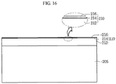
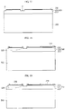
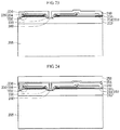
- Fig. 14a is a plan projection view of a light-emitting element 200 according to another embodiment
- Fig. 14b is an enlarged cross-sectional view taken along line A-A' of Fig. 14a .
- the light-emitting element 200 may include: a first conductivity type semiconductor layer 212; a second conductivity type semiconductor layer 216 disposed below the first conductivity type semiconductor layer 212; an active layer 214 disposed between the first conductivity type semiconductor layer 212 and the second conductivity type semiconductor layer 216; a plurality of holes H exposing parts of the first conductivity type semiconductor layer 212 to the bottom surface of the second conductivity type semiconductor layer 216 by penetrating the second conductivity type semiconductor layer 216 and the active layer 214; first contact electrodes 260 electrically connected to the first conductivity type semiconductor layer 212 from the bottom surface of the second conductivity type semiconductor layer 216 through the plurality of holes H; an insulation layer 240 disposed between the first contact electrodes 260 and the plurality of holes H; a first electrode layer 250 electrically connected to the first contact electrodes 260; and second contact electrodes 232 electrically connected to the second conductivity type semiconductor layer 216.
- the first conductivity type semiconductor layer 212, the second conductivity type semiconductor layer 216, and the active layer 214 may be collectively referred to as a light-emitting structure layer 210.
- Another embodiment may provide a high-efficiency low-current light-emitting element chip structure.
- another embodiment may include a division layer 290 which divides the light-emitting structure layer 210 into a plurality of cells C.
- the division layer 290 may include an insulating material.
- the division layer 290 may be made of an insulating material selected from SiOx, SiO x Ny, Al 2 O 3 , and TiO 2 , and may be made of a mixture of the insulating material and a light-reflecting material.
- the division layer 290 may be made of a mixture of the insulating material and one or more materials selected from Ag, Ni, Al, Rh, Pd, Ir, Ru, Mg, Zn, Pt, Au, and Hf.
- a height of the division layer 290 may start from the second conductivity type semiconductor layer 216 and the division layer 290 may penetrate the active layer 214 and the first conductivity type semiconductor layer 212.
- the division layer 290 may penetrate the undoped semiconductor layer and contact the passivation layer 270.
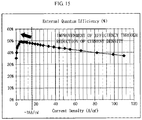
- Fig. 15 is a luminous efficiency graph of a light-emitting element according to another embodiment.
- each cell C has a low resistance because a volume of an epi-structure is reduced, and each cell C can perform a low-current operation at the same voltage because the cells S are electrically connected in parallel.
- the cell C can operate at about 18 A/cm 2 and external quantum efficiency increases because high-current injection is not involved.
- a light-emitting structure layer 210 may be formed above a growth substrate 205.
- the light-emitting structure layer 210 may include a first conductivity type semiconductor layer 212, an active layer 214, and a second conductivity type semiconductor layer 216.
- the growth substrate 205 is loaded into a growth apparatus, and a layer or a pattern may be formed above the growth substrate 205 by using a compound semiconductor of group II to VI elements.
- the growth apparatus may employ an electron beam evaporator, a PVD apparatus, a CVD apparatus, a PLD apparatus, a dual-type thermal evaporator, a sputtering apparatus, an MOCVD apparatus, or the like, but is not limited to these apparatuses.
- the growth substrate 205 may be a conductive substrate or an insulating substrate.
- the growth substrate 205 may be selected from the group consisting of a sapphire substrate (Al 2 0 3 ), GaN, SiC, ZnO, Si, GaP, InP, Ga 2 0 3 , and GaAs.
- a buffer layer (not illustrated) may be formed above the growth substrate 205.
- the buffer layer reduces a difference of a lattice constant between the growth substrate 205 and a nitride semiconductor layer and may be made of a material selected from GaN, AlN, AlGaN, InGaN, InN, InAlGaN, AlInN, AlGaAs, GaP, GaAs, GaAsP, and AlGaInP.
- the undoped semiconductor layer may be formed above the buffer layer.
- the undoped semiconductor layer may be made of an undoped GaN-based semiconductor.
- the undoped semiconductor layer may be a semiconductor layer having lower conductivity than that of an n-type semiconductor layer.
- a first conductivity type semiconductor layer 212 may be formed above the buffer layer or the undoped semiconductor layer. Subsequently, an active layer 214 may be formed above the first conductivity type semiconductor layer 212, and a second conductivity type semiconductor layer 216 may be sequentially stacked above the active layer 214.
- Another layer may be further disposed above or below each of the above-described semiconductor layers.
- a superlattice structure may be formed by using a group III-V compound semiconductor layer, but the present invention is not limited thereto.
- the first conductivity type semiconductor layer 212 may be selected from compound semiconductors of group III-V elements doped with a first conductive dopant, for example, GaN, AlN, AlGaN, InGaN, InN, InAlGaN, AlInN, AlGaAs, GaP, GaAs, GaAsP, and AlGaInP.
- the first conductivity type semiconductor layer 212 may be a semiconductor layer having an empirical formula of In x Al y Ga 1-x-y N (0 ⁇ x ⁇ 1, 0 ⁇ y ⁇ 1, 0 ⁇ x+y ⁇ 1) .
- the first conductivity type semiconductor layer 212 may be a n-type semiconductor layer, and the first conductive dopant may include an n-type dopant such as Si, Ge, Sn, Se, and Te.
- the first conductivity type semiconductor layer 212 may be a single layer or a multi-layer, and may have a superlattice structure in which two different layers selected from GaN, AlN, AlGaN, InGaN, InN, InAlGaN, AlInN, AlGaAs, GaP, GaAs, GaAsP, and AlGaInP are alternately disposed.
- the active layer 214 may have a single quantum well structure, a multiple quantum well structure, a quantum wire structure, or a quantum dot structure.
- the active layer 214 may be formed by using a compound semiconductor material of group III-V elements in a cycle of a well layer and a barrier layer.
- the well layer may include a semiconductor layer having an empirical formula of In x Al y Ga 1-x-y N (0 ⁇ x ⁇ 1, 0 ⁇ y ⁇ 1, 0 ⁇ x+y ⁇ 1)
- the barrier layer may include a semiconductor layer having an empirical formula of In x Al y Ga 1-x-y N (0 ⁇ x ⁇ 1, 0 ⁇ y ⁇ 1, 0 ⁇ x+y ⁇ 1).
- the barrier layer may be made of a material having a higher band gap than that of the well layer.
- the active layer 214 may have at least one cycle selected from, for example, a cycle of InGaN well layer/GaN barrier layer, a cycle of InGaN well layer/AlGaN barrier layer, and a cycle of InGaN well layer/InGaN barrier layer.
- the second conductivity type semiconductor layer 216 may be formed above the active layer 214, and the second conductivity type semiconductor layer 216 may be selected from compound semiconductors of group III-V elements doped with a second conductive dopant, for example, GaN, AlN, AlGaN, InGaN, InN, InAlGaN, AlInN, AlGaAs, GaP, GaAs, GaAsP, and AlGaInP.
- the second conductivity type semiconductor layer 216 may be a semiconductor layer having an empirical formula of In x Al y Ga 1-x-y N (0 ⁇ x ⁇ 1, 0 ⁇ y ⁇ 1, 0 ⁇ x+y ⁇ 1) .
- the second conductivity type semiconductor layer 216 may be a p-type semiconductor layer, and the second conductive dopant may include a p-type dopant such as Mg and Zn.
- the second conductivity type semiconductor layer 216 may be a single layer or a multi-layer, but is not limited thereto.
- the second conductivity type semiconductor layer 216 may have a superlattice structure in which two different layers selected from GaN, AlN, AlGaN, InGaN, InN, InAlGaN, AlInN, AlGaAs, GaP, GaAs, GaAsP, and AlGaInP are alternately disposed.
- the first conductivity type semiconductor layer 212, the active layer 214, and the second conductivity type semiconductor layer 216 may be defined as a light-emitting structure layer 210. Additionally, a third conductivity type semiconductor layer (not illustrated), for example, a semiconductor layer having an opposite polarity to the second conductivity type semiconductor layer, may be formed above the second conductivity type semiconductor layer 216.
- the light-emitting structure layer 210 may include at least one selected from an n-p junction structure, a p-n junction structure, an n-p-n junction structure, and a p-n-p junction structure.
- the second conductivity type semiconductor layer 216 is disposed on the uppermost layer of the light-emitting structure layer 210.
- a mesa etching process may be performed to remove a part of the light-emitting structure.
- a plurality of holes H exposing parts of the first conductivity type semiconductor layer 212 by penetrating the second conductivity type semiconductor layer 216 and the active layer 214 may be formed.
- the plurality of holes H may form a predetermined angle from the first conductivity type semiconductor layer 212 to the top surface of the second conductivity type semiconductor layer 216, for example, an obtuse angle with respect to the top surface of the light-emitting structure layer 210.
- a horizontal width of the plurality of holes H may be gradually reduced downward.
- the horizontal width of the plurality of holes H may be gradually reduced upward.
- the removed regions of the active layer 214 and the first conductivity type semiconductor layer 212 may be reduced, contributing to luminous efficiency.
- a channel layer 220 may be formed above the plurality of holes H.
- the channel layer 220 may not be formed in a region where a first contact electrode 260 is to be formed. In this way, a part of the first conductivity type semiconductor layer 212 may be exposed.
- the channel layer 220 serves as an electrically insulating layer between the first contact electrode 260 to be formed, the active layer 214, and the second conductivity type semiconductor layer 216.
- the channel layer 220 may be made of one or more materials selected from SiO x , SiO x Ny, Al 2 O 3 , and TiO 2 .
- the reflectivity of the channel layer 220 may exceed 50%.
- the channel layer 220 may be made of an insulating material selected from SiO 2 , SiO x , SiO x Ny, Si 3 N 4 , Al 2 O 3 , and TiO 2 , and may be made of a mixture of the insulating material and a light-reflecting material.
- the channel layer 220 may be made of a mixture of the insulating material and one or more materials selected from Ag, Ni, Al, Rh, Pd, Ir, Ru, Mg, Zn, Pt, Au, and Hf.
- the channel layer 220 when the emitted light travels downward, the channel layer 220 also reflects the light, thereby minimizing light absorption and increasing luminous efficiency.
- a second contact electrode 232 may be formed above the second conductivity type semiconductor layer 216.
- the second contact electrode 232 ohmic-contacts the second conductivity type semiconductor layer 216.
- the second contact electrode 232 may include at least one conductive material and may be a single layer or a multi-layer.
- the second contact electrode 232 may include at least one of a metal, a metal oxide, and a metal nitride.
- the second contact electrode 232 may include a light-transmitting material.
- the second contact electrode 132 may include at least one of ITO, IZO, IZON, IZTO, IAZO, IGZO, IGTO, AZO, ATO, GZO, IrO x , RuO x , RuO x /ITO, Ni/IrO x /Au, Ni/IrO x /Au/ITO, Pt, Ni, Au, Rh, and Pd.
- a first contact electrode 260 may be formed above the exposed first conductivity type semiconductor layer 212.
- the first contact electrode 260 may ohmic-contact the exposed first conductivity type semiconductor layer 212. When viewed from above, the first contact electrode 260 may have a circular or polygonal shape, but is not limited thereto.
- the top surface of the first contact electrode 260 may be disposed between the top surface of the active layer 214 and the top surface of the first conductivity type semiconductor layer 212.
- the surface of the first conductivity type semiconductor layer 212, which contacts the first contact electrode 260, may be formed to have a flat structure as a Ga-face, but is not limited thereto.
- the width of the first contact electrode 260 may gradually increase toward the top surface from the bottom surface.
- the width of first contact electrode 260 may be gradually reduced toward the bottom surface from the top surface.
- a horizontal width of the bottom surface of the first contact electrode 260 matches a horizontal width of a diffusion barrier layer 254 contacting the first contact electrode 260.
- a reflection layer 234 may be formed above the second contact electrode 232.
- the reflection layer 234 may be disposed above the second contact electrode 232 and may reflect light incident through the second contact electrode 232.
- the reflection layer 234 may include a metal.
- the reflection layer 134 may be a single layer or a multi-layer made of a material selected from Ag, Ni, Al, Rh, Pd, Ir, Ru, Mg, Zn, Pt, Au, Hf, and an alloy of two or more of the listed materials.
- a capping layer 236 may be formed above the reflection layer 234.
- the second contact electrode 232, the reflection layer 234, and the capping layer 236 may be collectively referred to as a second electrode layer 230.
- the second electrode layer 230 may supply the power from a pad electrode 280 to the second conductivity type semiconductor layer 216.
- the capping layer 236 may be disposed above the reflection layer 234 to supply the power from the pad electrode 280 to the reflection layer 234.
- the capping layer 236 may function as a current-spreading layer.
- the capping layer 236 may include a metal and may include at least one of Sn, Ga, In, Bi, Cu, Ni, Ag, Mo, Al, Au, Nb, W, Ti, Cr, Ta, Al, Pd, Pt, Si, and selective alloys thereof as a material having high conductivity.
- an insulation layer 240 may be formed above the capping layer 236 and the channel layer 220.
- the insulation layer 240 may be formed to expose the first contact electrode 260.
- the insulation layer 240 electrically insulates the first contact electrode 260 from other semiconductor layers.
- the insulation layer 240 may be disposed between a first electrode layer 250 to be formed and the channel layer 220 to block electrical contact therebetween.
- the insulation layer 240 may be made of a material selected from SiO 2 , SiO x , SiO x N y , Si 3 N 4 , Al 2 O 3 , and TiO 2 .
- the reflectivity of the insulation layer 240 may exceed 50%.
- the insulation layer 240 may be made of an insulating material selected from SiO 2 , SiO x , SiO x N y , Si 3 N 4 , Al 2 O 3 , and TiO 2 , and may be made of a mixture of the insulating material and a light-reflecting material.
- the insulation layer 240 may be made of a mixture of the insulating material and one or more materials selected from Ag, Ni, Al, Rh, Pd, Ir, Ru, Mg, Zn, Pt, Au, and Hf.
- a physical property of the insulation layer 240 formed between the first contact electrode 260 and the plurality of holes H is formed by a reflection layer material, so that light absorption in the insulation layer 240 performing a passivation function is minimized, thereby increasing luminous efficiency.
- a thickness of the insulation layer 240 may be in a range of about 1 ⁇ m to about 2 ⁇ m.
- a thickness ratio of the insulation layer 240 formed between the first contact electrode 260 and the plurality of holes H is optimally controlled to perform a shorting prevention function and prevent a reduction in luminous efficiency.
- the light-emitting element according to another embodiment can increase luminous efficiency by controlling a thickness ratio or a physical property of the passivation layer.
- a diffusion barrier layer 254 may be formed above the insulation layer 240 and the first contact electrode 260, and a bonding layer 256 may be formed above the diffusion barrier layer 254
- the diffusion barrier layer 254 and/or the bonding layer 256 may include at least one of Ti, Au, Sn, Ni, Cr, Ga, In, Bi, Cu, Ag, and Ta.
- the diffusion barrier layer 254 and/or the bonding layer 256 may be formed by using at least one of a deposition method, a sputtering method, and a plating method, and may be attached with a conductive sheet.
- the bonding layer 256 may not be formed, but the present invention is not limited thereto.
- a support member 258 may be formed above the bonding layer 256.
- the diffusion barrier layer 254, the bonding layer 256, and the support member 258 may be collectively referred to as a first electrode layer 250, and the first electrode layer 250 may supply power from a lower electrode 259 to the first conductivity type semiconductor layer 212.
- the support member 258 may be bonded to the bonding layer 256, but is not limited thereto.
- the support member 258 may be a conductive support member, and a base substrate of the support member 158 may be at least one of Cu, Au, Ni, Mo, and Cu-W.
- the support member 258 may be realized by a carrier wafer (e.g., Si, Ge, GaAs, ZnO, SiC, SiGe, Ga 2 0 3 , GaN, etc.), and may be bonded on a circuit pattern of a board or a lead frame of a package by solder.
- a carrier wafer e.g., Si, Ge, GaAs, ZnO, SiC, SiGe, Ga 2 0 3 , GaN, etc.
- the growth substrate 205 may be removed.
- the surface of the first conductivity type semiconductor layer 212 may be exposed by removing the undoped semiconductor layer (not illustrated) or the like remaining after the removal of the growth substrate 205.
- the growth substrate 205 may be removed by a physical and/or chemical method.
- the growth substrate 205 may be removed by an LLO process.
- the growth substrate 205 is lifted off by a method of irradiating a laser beam having a wavelength of a predetermined region on the growth substrate 205.
- the growth substrate 205 may be separated by removing the buffer layer (not illustrated) by using a wet etching solution, wherein the buffer layer is disposed between the growth substrate 205 and the first conductivity type semiconductor layer 212.
- the top surface of the first conductivity type semiconductor layer 212 may be exposed by removing the growth substrate 205 and removing the buffer layer through etching or polishing.
- the top surface of the first conductivity type semiconductor layer 212 is an N-face, and may be a surface closer to the growth substrate.
- the top surface of the first conductivity type semiconductor layer 212 may be etched by inductively coupled plasma/reactive ion etching (ICP/RIE) or the like, or may be polished by a polishing apparatus.
- ICP/RIE inductively coupled plasma/reactive ion etching
- a part of the light-emitting structure layer 210 may be removed to expose a part of the channel layer 220.
- parts of the first conductivity type semiconductor layer 212, the active layer 214, and the second conductivity type semiconductor layer 216 in the region where the pad electrode 280 is to be formed may be removed.
- a periphery of the light-emitting structure layer 210 i.e., a channel region or an isolation region that is a boundary between chips, may be removed by performing wet etching or dry etching, and the channel layer 220 may be exposed.
- a light extraction structure may be formed on the top surface of the first conductivity type semiconductor layer 212, and the light extraction structure may be formed to have a roughness or a pattern.
- the light extraction structure may be formed by wet etching or dry etching.
- Another embodiment may include a division layer 290 which divides the light-emitting structure layer 210 into a plurality of cells C. In this way, another embodiment may provide a high-efficiency low-current light-emitting element chip structure.
- a height of the division layer 290 may start from the second conductivity type semiconductor layer 216 and the division layer 290 may penetrate the active layer 214 and the first conductivity type semiconductor layer 212.
- the division layer 290 may penetrate the undoped semiconductor layer and contact the passivation layer 270.
- the division layer 290 may include an insulating material.
- the division layer 290 may be made of an insulating material selected from SiO 2 , SiO x , SiO x Ny, Si 3 N 4 , Al 2 O 3 , and TiO 2 , and may be made of a mixture of the insulating material and a light-reflecting material.
- the division layer 290 may be made of a mixture of the insulating material and one or more materials selected from Ag, Ni, Al, Rh, Pd, Ir, Ru, Mg, Zn, Pt, Au, and Hf.
- each cell C has a low resistance because a volume of an epi-structure is reduced, and each cell C can perform a low-current operation at the same voltage because the cells S are electrically connected in parallel.
- a passivation layer 270 may be formed above the exposed channel layer 220 and the light-emitting structure layer 210.
- parts of the passivation layer 270 and the channel layer 220 in a region where a pad electrode 180 is to be formed may be removed to expose a part of the capping layer 236.
- the passivation layer 270 may be made of a material selected from SiO x N y , Si 3 N 4 , Al 2 O 3 , and TiO 2 .
- a pad electrode 280 may be formed above the exposed capping layer 236.
- the pad electrode 280 may be made of Ti/Au or the like, but is not limited thereto.
- the pad electrode 280 is a region to be bonded with a wire and may be disposed in a predetermined region of the light-emitting structure layer 210.
- the pad electrode 280 may be provided with one or more pad electrodes.
- a first electrode 259 may be formed below the first electrode layer 250.
- the first electrode 259 may be made of a material having high conductivity, for example, Ti, Al, or Ni, but is not limited thereto.
- luminous efficiency can be increased by controlling a thickness ratio or a physical property of the passivation layer.
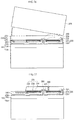
- Fig. 30 is a view of a light-emitting element package to which the light-emitting element according to an embodiment is applied.
- the light-emitting element package may include a body 305, a first lead electrode 313 and a second lead electrode 314 disposed in the body 305, a light-emitting element 200 provided in the body 305 and electrically connected to the first lead electrode 313 and the second lead electrode 314, and a molding member 340 surrounding the light-emitting element 200.
- the body 305 may be made of a silicon material, a synthetic resin material, or a metal material, and may have an inclined surface around the light-emitting element 100.
- the first lead electrode 313 and the second lead electrode 314 are electrically separated from each other and supply power to the light-emitting element 200. Additionally, the first lead electrode 313 and the second lead electrode 314 may reflect light generated by the light-emitting element 200 to thereby increase luminous efficiency, and may serve to discharge heat generated by the light-emitting element 200 to the outside.
- the light-emitting element 200 may be disposed above the body 305, or may be disposed above the first lead electrode 313 or the second lead electrode 314.
- the light-emitting element 100 may be electrically connected to the first lead electrode 313 and the second lead electrode 314 by any one of a wire method, a flip-chip method, and a die bonding method.
- the light-emitting element 200 may be mounted on the second lead electrode 314 and may be connected to the first lead electrode 313 by a wire 350, but the embodiment is not limited thereto.
- the molding member 340 may surround the light-emitting element 200 so as to protect the light-emitting element 200. Additionally, the molding member 340 may include a phosphor 322 so as to change a wavelength of the light emitted by the light-emitting element 200.
- a plurality of light-emitting elements or light-emitting element packages according to the embodiment may be arrayed above a substrate, and optical members, such as lens, a polarizing plate, a prism sheet, and a diffusion sheet, may be disposed on an optical path of the light-emitting element package.
- the light-emitting element package, the substrate, and the optical members may function as a light unit.
- the light unit may be implemented in a top view type or a side view type, may be provided to display devices of a mobile terminal, a notebook computer, and the like, or may be variously applied to a lighting device, an indicating device, and the like.
- Further another embodiment may be implemented as a lighting system including the light-emitting element or the light-emitting element package described in the above embodiments.
- the lighting system may include a lamp, a streetlight, an electronic display, and a headlight.
- Fig. 31 is an exploded perspective view of a lighting system according to an embodiment.
- the lighting system according to the embodiment may include a cover 3100, a light source module 3200, a radiator 3300, a power supply unit 3400, an inner case 3500, and a socket 3600. Additionally, the lighting system according to the embodiment may further include a member 3300 and/or a holder 3500.
- the light source module 3200 may include the light-emitting element package according to the embodiment.
- the cover 3100 may have a bulb or semispherical shape and may be hollow, and a part of the cover 3100 may be opened.
- the cover 3100 may be optically coupled to the light source module 3200.
- the cover 3100 may diffuse, scatter, or excite light provided from the light source module 3200.
- the cover 3100 may be a type of optical member.
- the cover 3100 may be coupled to the radiator 3300.
- the cover 3100 may have a coupling portion which is coupled to the radiator 3300.
- the inner surface of the cover 3100 may be coated with a milk-white paint.
- the milk-white paint may include a diffusion material which diffuses light.
- a surface roughness of the inner surface of the cover 3100 may be greater than a surface roughness of the outer surface of the cover 3100, so as to sufficiently scatter and diffuse the light from the light source module 3200 and discharge the light to the outside.
- a material of the cover 3100 may include glass, plastic, polypropylene (PP), polyethylene (PE), polycarbonate (PC), and the like.
- the polycarbonate (PC) has superior light resistance, heat resistance and strength.
- the cover 3100 may be transparent so that a user can view the light source module 3200 from the outside, or may be opaque.
- the cover 3100 may be formed through blow molding.
- the light source module 3200 may be disposed on one surface of the radiator 3300. Accordingly, the heat from the light source module 3200 is transferred to the radiator 3300.
- the light source module 3200 may include a light source unit 3210, a connection plate 3230, and a connector 3250.
- the member 3300 is disposed on the radiator 3300 and includes guide grooves 3310 into which a plurality of light source units 3210 and the connector are inserted.
- the guide grooves 3310 corresponds to the substrate of the light source unit 3210 and the connector 3250.
- a surface of the member 3300 may be deposited or coated with a light-reflecting material.
- a surface of the member 3300 may be deposited or coated with a white paint.
- the member 3300 reflects light, which is reflected by the inner surface of the cover 3100 and is returned toward the light source module 3200, again toward the cover 3100. Accordingly, the luminous efficiency of the lighting system according to the embodiment may be improved.
- the member 3300 may include, for example, an insulating material.
- the connection plate 3230 of the light source module 3200 may include an electrically conductive material. Accordingly, the radiator 3300 may electrically contact the connection plate 3230. Since the member 3300 is made of an insulating material, the member 3300 may prevent electrical shorting between the connection plate 3230 and the radiator 3300.
- the radiator 3300 receives heat from the light source module 3200 and the power supply unit 3400 and radiates the heat.
- the holder 3500 covers an accommodation groove 3719 of an insulating portion 3710 of the inner case 3500 Accordingly, the power supply unit 3400 accommodated in the insulating portion 3710 of the inner case 3500 is tightly sealed.
- the holder 3500 includes a guide protrusion 3510.
- the guide protrusion 3510 has a hole through which a protrusion 3610 of the power supply unit 3400 penetrates.
- the power supply unit 3400 processes or converts an electric signal received from the outside and provides the processed or converted electric signal to the light source module 3200.
- the power supply unit 3400 is accommodated in the accommodation groove 3719 of the inner case 3500 and is sealed inside the inner case 3500 by the holder 3500.
- the power supply unit 3400 may include a protrusion 3610, a guide portion 3630, a base 3650, and an extension portion 3670.
- the guide portion 3630 has a shape protruding outward from one side of the base 3650.
- the guide portion 3630 may be inserted into the holder 3500.
- a plurality of components may be disposed above one surface of the base 3650.
- the plurality of components may include, for example, a DC converter which converts AC power supplied from an external power supply into DC power, a driving chip which controls driving of the light source module 3200, and electrostatic discharge (ESD) protection device which protects the light source module 3200, but is not limited thereto.
- the extension portion 3670 has a shape protruding outward from anther side of the base 3650.
- the extension portion 3670 is inserted into the connection portion 3750 of the inner case 3500 and receives an electric signal from the outside.
- a width of the extension portion 3670 may be equal to or less than a width of the connection portion 3750 of the inner case 3500.
- One end of a positive (+) wire and one end of a negative (-) wire may be electrically connected to the extension portion 3670, and the other end of the positive (+) wire and the other end of the negative (-) wire may be electrically connected to the socket 3600.
- the inner case 3500 may include a molding portion therein together with the power supply unit 3400.
- the molding portion is provided by hardening a molding liquid and may fix the power supply unit 3400 to the inside of the inner case 3500.
Description
- An embodiment relates to a light-emitting element.
- A light-emitting element (light-emitting device) is a p-n junction diode which converts electrical energy into light energy. The light-emitting element may be produced using compound semiconductors of groups III and V in the periodic table, and may implement various colors by adjusting a composition ratio of the compound semiconductors.
- The light-emitting element emits energy corresponding to a band-gap energy between a conduction band and a valence band when electrons of an n-type layer and holes of a p-type layer recombine upon application of a forward voltage. This energy is usually emitted in the form of heat or light. The light-emitting element emits the energy in the form of light.
- For example, a nitride semiconductor has received much attention in development fields of optical devices and high-power electronic devices due to its high thermal stability and wide band-gap energy. In particular, a blue light-emitting element, a green light-emitting element, an ultraviolet (UV) light-emitting element, and the like using the nitride semiconductor have become commercialized and are widely used.
- An example of a light-emitting element according to the related art is a lateral-type light-emitting element in which an electrode layer is disposed in one direction of an epi-layer. In the lateral-type light-emitting element, an operating voltage (Vf) of the light-emitting element increases due to a narrow current flow, causing a reduction in current efficiency. Thus, there is a problem that the lateral-type light-emitting element is vulnerable to electrostatic discharge.
- In order to solve such a problem, a via hole-based vertical-type light-emitting element has been developed. In the via hole-based vertical-type light-emitting element, a via hole is formed below an epi-layer and an electrode is disposed therein.
- In the related art, in order to produce the via hole-based vertical-type light-emitting element, a plurality of mesa etching processes are performed for forming an n-contact, and an insulation layer is formed between the n-contact and a mesa etching hole.
- According to the related art, electrons injected through a via hole cause an electron clouding phenomenon in the vicinity of the via hole, and these electrons flow through the vicinity of the via hole. Thus, light is generated in only a partial region of an active layer and luminous flux is low accordingly.
- The documents
US 2011/049555 A1 ,EP 2439796 A1 ,EP 2439794 A1 ,US 2014/048838 A1 ,US 2008/237622 A1 ,DE 10 2011 056888 A1 describe examples of light-emitting elements. - An embodiment provides a light-emitting element capable of improving luminous flux.
- A light-emitting element according to claims 1 to 6 is provided.
- According to embodiments, it is possible to provide a light-emitting element capable of improving luminous flux.
- According to embodiments, it is possible to provide a large-sized light-emitting element which exhibits high optical efficiency at a low current.
-
-
Fig. 1 is a plan projection view of a light-emitting element according to an embodiment forming part of the invention. -
Fig. 2 is an enlarged cross-sectional view of a light-emitting element according to an embodiment forming part of the invention. -
Figs. 3 to 13 are process cross-sectional views of a method for producing a light-emitting element according to an embodiment forming part of the invention. -
Fig. 14a is a plan projection view of a light-emitting element according to another embodiment, which does not form part of the invention. -
Fig. 14b is an enlarged cross-sectional view of a light-emitting element according to another embodiment, which does not form part of the invention. -
Fig. 15 is a luminous efficiency graph of a light-emitting element according to another embodiment, which does not form part of the invention. -
Figs. 16 to 29 are process cross-sectional views of a method for producing a light-emitting element according to another embodiment, which does not form part of the invention. -
Fig. 30 is a cross-sectional view of a light-emitting element package according to an embodiment, which does not form part of the invention. -
Fig. 31 is an exploded perspective view of a lighting system according to an embodiment, which does not form part of the invention. - In the description of embodiments, it will be understood that when a layer (film), region, pattern, or structures is referred to as being "on/above" or "below/under" a substrate, another layer (film), region, pad, or patterns, it can be directly on or below another layer (film), region, pad, or patterns, and one or more intervening layer may also be present therebetween. Additionally, the criteria for "on/above" and "below/under" is based on the drawings.
- The invention is defined by the appended claims. Only the embodiment described in relation with
Figures 1-13 is an embodiment of the invention. All other embodiments of the present disclosure are not claimed and merely represent comparative examples useful for understanding the invention. -
Fig. 1 is a plan projection view of a light-emittingelement 100 according to an embodiment of the invention, andFig. 2 is an enlarged cross-sectional view taken along line A-A' ofFig. 1 . - The light-
emitting element 100 according to the embodiment includes: a first conductivitytype semiconductor layer 112; a second conductivitytype semiconductor layer 116 disposed below the first conductivitytype semiconductor layer 112; anactive layer 114 disposed between the first conductivitytype semiconductor layer 112 and the second conductivitytype semiconductor layer 116; a plurality of holes H exposing parts of the first conductivitytype semiconductor layer 112 to the bottom surface of the second conductivitytype semiconductor layer 116 by penetrating the second conductivitytype semiconductor layer 116 and theactive layer 114;first contact electrodes 160 electrically connected to the first conductivitytype semiconductor layer 112 from the bottom surface of the second conductivitytype semiconductor layer 116 through the plurality of holes H; aninsulation layer 140 disposed between thefirst contact electrodes 160 and the plurality of holes H; afirst electrode layer 150 electrically connected to thefirst contact electrodes 160; and asecond contact electrode 132 electrically connected to the second conductivitytype semiconductor layer 116. - The
first electrode layer 150 may include abonding layer 156 electrically connected to thefirst contact electrodes 160, and asupport member 158 disposed below thebonding layer 156. - The embodiment is directed to providing the light-emitting element capable of improving luminous flux.
- To this end, the embodiment includes a first current-spreading
semiconductor layer 191 inside the first conductivitytype semiconductor layer 112 above thefirst contact electrode 160. - The first current-spreading
semiconductor layer 191 includes a first conductive AlGaN/GaN superlattice layer or a first conductive AlGaN/GaN/InGaN superlattice layer. - According to the embodiment, since the first current-spreading
semiconductor layer 191 made of n-AlGaN/GaN SLs or n-AlGaN/GaN/InGaN SLs is disposed above thefirst contact electrodes 160 formed in the via hole H, injected electrons flow while spreading in a lateral direction and the electrons are injected into an entire area of an active layer (MQW). Thus, a larger light emission area is provided as compared to an existing structure. - The embodiment further includes a second current-spreading
semiconductor layer 192 between theactive layer 114 and the first conductivitytype semiconductor layer 112. The first current-spreadingsemiconductor layer 191 and the second current-spreadingsemiconductor layer 192 may be collectively referred to as a current-spreadingsemiconductor layer 190. - In the embodiment, the second current-spreading
semiconductor layer 192 is disposed to be lower than thefirst contact electrodes 160. - According to the embodiment, the electrons injected by the
first contact electrodes 160 or the electrons spread from the first current-spreadingsemiconductor layer 191 are additionally spread by arranging the second current-spreadingsemiconductor layer 192 between theactive layer 114 and the first conductivitytype semiconductor layer 112. Thus, carrier injection efficiency may be improved to increase luminous flux. - According to the embodiment, it is possible to provide a light-emitting element capable of improving luminous flux, and comparative examples can provide the method for producing the same, a light-emitting element package, and a lighting system.
- Hereinafter, a method for producing a light-emitting element according to an embodiment will be described with reference to
Figs. 3 to 13 . - First, as illustrated in
Fig. 3 , a light-emitting structure layer 110 may be formed above agrowth substrate 105. The light-emitting structure layer 110 includes a first conductivitytype semiconductor layer 112, anactive layer 114, and a second conductivitytype semiconductor layer 116. - The embodiment includes a current-spreading
semiconductor layer 190 for increasing luminous flux, and the current-spreadingsemiconductor layer 190 includes a first current-spreadingsemiconductor layer 191 and a second current-spreadingsemiconductor layer 192. - The embodiment includes the first current-spreading
semiconductor layer 191 formed inside the first conductivitytype semiconductor layer 112. - The first current-spreading
semiconductor layer 191 includes a first conductive AlGaN/GaN superlattice layer or a first conductive AlGaN/GaN/InGaN superlattice layer. - Referring to
Fig. 2 , in the embodiment, since the first current-spreadingsemiconductor layer 191 made of n-AlGaN/GaN SLs or n-AlGaN/GaN/InGaN SLs is disposed above afirst contact electrodes 160 to be formed later, injected electrons flow while spreading in a lateral direction and the electrons are injected into an entire area of an active layer (MQW). Thus, a larger light emission area is provided as compared to an existing structure. - The embodiment further includes a second current-spreading
semiconductor layer 192 between theactive layer 114 and the first conductivitytype semiconductor layer 112. - In the embodiment, the second current-spreading
semiconductor layer 192 is disposed to be lower than thefirst contact electrodes 160 to be formed later. - According to the embodiment, the electrons injected by the
first contact electrodes 160 or the electrons spread from the first current-spreadingsemiconductor layer 191 are additionally spread by arranging the second current-spreadingsemiconductor layer 192 between theactive layer 114 and the first conductivitytype semiconductor layer 112. Thus, carrier injection efficiency may be improved to increase luminous flux. - According to the embodiment, it is possible to provide the light-emitting element capable of improving luminous flux.
- In the embodiment, the first conductivity
type semiconductor layer 112 includes afirst semiconductor layer 112a of a first conductivity type above thegrowth substrate 105, and a firstsecond semiconductor layer 112b of the first conductivity type formed after the first current-spreading semiconductor layer 101 is formed. - The
growth substrate 105 is loaded into a growth apparatus, and a layer or a pattern may be formed above thegrowth substrate 105 by using a compound semiconductor of group II to VI elements. - The growth apparatus may employ an electron beam evaporator, a physical vapor deposition (PVD) apparatus, a chemical vapor deposition (CVD) apparatus, a plasma laser deposition (PLD) apparatus, a dual-type thermal evaporator, a sputtering apparatus, a metal organic chemical vapor deposition (MOCVD) apparatus, or the like, but is not limited to these apparatuses.
- The
growth substrate 105 may be a conductive substrate or an insulating substrate. For example, thegrowth substrate 105 may be selected from the group consisting of a sapphire substrate (Al2O3), GaN, SiC, ZnO, Si, GaP, InP, Ga2O3, and GaAs. - A buffer layer (not illustrated) may be formed above the
growth substrate 105. The buffer layer reduces a difference of a lattice constant between thegrowth substrate 105 and a nitride semiconductor layer and may be made of a material selected from GaN, AlN, AlGaN, InGaN, InN, InAlGaN, AlInN, AlGaAs, GaP, GaAs, GaAsP, and AlGaInP. - An undoped semiconductor layer (not illustrated) may be formed above the buffer layer. The undoped semiconductor layer may be made of an undoped GaN-based semiconductor. The undoped semiconductor layer may be a semiconductor layer having lower conductivity than that of an n-type semiconductor layer.
- Subsequently, a first conductivity
type semiconductor layer 112 is formed above the buffer layer or the undoped semiconductor layer. Subsequently, anactive layer 114 is formed above the first conductivitytype semiconductor layer 112, and a second conductivitytype semiconductor layer 116 is sequentially stacked above theactive layer 114. - Another layer may be further disposed above or below each of the above-described semiconductor layers. For example, a superlattice structure may be formed by using a group III-V compound semiconductor layer, but the present invention is not limited thereto.
- The first conductivity
type semiconductor layer 112 may be selected from compound semiconductors of group III-V elements doped with a first conductive dopant, for example, GaN, AlN, AlGaN, InGaN, InN, InAlGaN, AlInN, AlGaAs, GaP, GaAs, GaAsP, and AlGaInP. For example, the first conductivitytype semiconductor layer 112 may be a semiconductor layer having an empirical formula of InxAlyGa1-x-yN (0≤ x≤ 1, 0≤ y≤ 1, 0≤ x+y≤ 1). - The first conductivity
type semiconductor layer 112 may be an n-type semiconductor layer, and the first conductive dopant may include an n-type dopant such as Si, Ge, Sn, Se, and Te. - The first conductivity
type semiconductor layer 112 may be a single layer or a multi-layer, and may have a superlattice structure in which two different layers selected from GaN, AlN, AlGaN, InGaN, InN, InAlGaN, AlInN, AlGaAs, GaP, GaAs, GaAsP, and AlGaInP are alternately disposed. - The
active layer 114 may have a single quantum well structure, a multiple quantum well structure, a quantum wire structure, or a quantum dot structure. Theactive layer 114 may be formed by using a compound semiconductor material of group III-V elements in a cycle of a well layer and a barrier layer. The well layer may include a semiconductor layer having an empirical formula of InxAlyGa1-x-yN (0≤ x≤ 1, 0≤ y≤ 1, 0≤ x+y≤ 1), and the barrier layer may include a semiconductor layer having an empirical formula of InxAlyGa1-x-yN (0≤ x≤ 1, 0 ≤ y≤ 1, 0≤ x+y≤ 1) . The barrier layer may be made of a material having a higher band gap than that of the well layer. - The
active layer 114 may have at least one cycle selected from, for example, a cycle of InGaN well layer/GaN barrier layer, a cycle of InGaN well layer/AlGaN barrier layer, and a cycle of InGaN well layer/InGaN barrier layer. - The second conductivity
type semiconductor layer 116 may be formed above theactive layer 114, and the second conductivitytype semiconductor layer 116 may be selected from compound semiconductors of group III-V elements doped with a second conductive dopant, for example, GaN, AlN, AlGaN, InGaN, InN, InAlGaN, AlInN, AlGaAs, GaP, GaAs, GaAsP, and AlGaInP. The second conductivitytype semiconductor layer 116 may be a semiconductor layer having an empirical formula of InxAlyGa1-x-yN (0≤ x≤ 1, 0≤ y≤ 1, 0≤ x+y≤ 1). - The second conductivity
type semiconductor layer 116 may be a p-type semiconductor layer, and the second conductive dopant may include a p-type dopant such as Mg and Zn. The second conductivitytype semiconductor layer 116 may be a single layer or a multi-layer, but is not limited thereto. - The second conductivity
type semiconductor layer 116 may have a superlattice structure in which two different layers selected from GaN, AlN, AlGaN, InGaN, InN, InAlGaN, AlInN, AlGaAs, GaP, GaAs, GaAsP, and AlGaInP are alternately disposed. - The first conductivity
type semiconductor layer 112, theactive layer 114, and the second conductivitytype semiconductor layer 116 may be defined as a light-emittingstructure layer 110. Additionally, a third conductivity type semiconductor layer (not illustrated), for example, a semiconductor layer having an opposite polarity to the second conductivity type semiconductor layer, may be formed above the second conductivitytype semiconductor layer 116. - Accordingly, the light-emitting
structure layer 110 may include at least one selected from an n-p junction structure, a p-n junction structure, an n-p-n junction structure, and a p-n-p junction structure. In the following description, it is assumed that the second conductivitytype semiconductor layer 116 is disposed on the uppermost layer of the light-emittingstructure layer 110. - Subsequently, as illustrated in
Fig. 4 , a mesa etching process may be performed to remove a part of the light-emittingstructure layer 110 and a part of the second current-spreadingsemiconductor layer 192. - A plurality of holes H exposing parts of the first conductivity
type semiconductor layer 112 by penetrating the second conductivitytype semiconductor layer 116, theactive layer 114, and the second current-spreadingsemiconductor layer 192 is formed. - In the embodiment, the plurality of holes H may form a predetermined angle from the first conductivity
type semiconductor layer 112 to the top surface of the second conductivitytype semiconductor layer 116, for example, an obtuse angle with respect to the top surface of the light-emittingstructure layer 110. - In the embodiment, a horizontal width of the plurality of holes H may be gradually reduced downward. On the other hand, in
Fig. 2 , the horizontal width of the plurality of holes H may be gradually reduced upward. - With reference to
Fig. 2 , according to the embodiment, since the horizontal width of the plurality of holes H is gradually reduced upward, the removed regions of theactive layer 114 and the first conductivitytype semiconductor layer 112 may be reduced, contributing to luminous efficiency. - Subsequently, as illustrated in
Fig. 5 , achannel layer 120 may be formed above the plurality of holes H. Thechannel layer 120 may not be formed in a region where afirst contact electrode 160 is to be formed. In this way, a part of the first conductivitytype semiconductor layer 112 may be exposed. - The
channel layer 120 may function as an electrically insulating layer between thefirst contact electrode 160 to be formed, theactive layer 114, and the second conductivitytype semiconductor layer 116. - The
channel layer 120 may be made of one or more materials selected from SiOx, SiOxNy, Al2O3, and TiO2. - Additionally, in the embodiment, the reflectivity of the
channel layer 120 may exceed 50%. For example, thechannel layer 120 may be made of an insulating material selected from SiO2, SiOx, SiOxNy, Si3N4, Al2O3, and TiO2, and may be made of a mixture of the insulating material and a light-reflecting material. - For example, the
channel layer 120 may be made of a mixture of the insulating material and one or more materials selected from Ag, Ni, Al, Rh, Pd, Ir, Ru, Mg, Zn, Pt, Au, and Hf. - According to the embodiment, when the emitted light travels downward, the
channel layer 120 also reflects the light, thereby minimizing light absorption and increasing luminous efficiency. - Subsequently, as illustrated in
Fig. 6 , asecond contact electrode 132 is formed above the second conductivitytype semiconductor layer 116. - The
second contact electrode 132 ohmic-contacts the second conductivitytype semiconductor layer 116. Thesecond contact electrode 132 includes at least one conductive material and may be a single layer or a multi-layer. - For example, the
second contact electrode 132 may include at least one of a metal, a metal oxide, and a metal nitride. - The
second contact electrode 132 may include a light-transmitting material. For example, thesecond contact electrode 132 may include at least one of indium tin oxide (ITO), indium zinc oxide (IZO), IZO nitride (IZON), indium zinc tin oxide (IZTO), indium aluminum zinc oxide (IAZO), indium gallium zinc oxide (IGZO), indium gallium tin oxide (IGTO), aluminum zinc oxide (AZO), antimony tin oxide (ATO), gallium zinc oxide (GZO), IrOx, RuOx, RuOx/ITO, Ni/IrOx/Au, Ni/IrOx/Au/ITO, Pt, Ni, Au, Rh, and Pd. - Subsequently, as illustrated in
Fig. 7 , afirst contact electrode 160 is formed above the exposed first conductivitytype semiconductor layer 112. - The
first contact electrode 160 may ohmic-contact the exposed first conductivitytype semiconductor layer 112. When viewed from above, thefirst contact electrode 160 may have a circular or polygonal shape, but is not limited thereto. - The top surface of the
first contact electrode 160 is disposed between the top surface of theactive layer 114 and the top surface of the first conductivitytype semiconductor layer 112. - The surface of the first conductivity
type semiconductor layer 112, which contacts thefirst contact electrode 160, may be formed to have a flat structure as a Ga-face, but is not limited thereto. - With reference to
Fig. 7 , in the embodiment, the width of thefirst contact electrode 160 may be gradually increased toward the top surface from the bottom surface. With reference toFig. 2 , the width of thefirst contact electrode 160 may be gradually reduced toward the bottom surface from the top surface. - In this way, a probability of shorting between the
first contact electrode 160 and asecond electrode layer 130 to be formed later is reduced, and a region occupied by thefirst contact electrode 160 is reduced while maximizing a region where thefirst contact electrode 160 contacts the first conductivitytype semiconductor layer 112, thereby increasing luminous efficiency. - When described with reference to
Fig. 2 , a horizontal width of the bottom surface of thefirst contact electrode 160 matches a horizontal width of adiffusion barrier layer 154 contacting thefirst contact electrode 160. Thus, it is possible to prevent deterioration of electrical characteristics while minimizing a region occupied by thediffusion barrier layer 154 and thefirst contact electrode 160. - Subsequently, as illustrated in
Fig. 8 , areflection layer 134 may be formed above thesecond contact electrode 132. - The
reflection layer 134 may be disposed above thesecond contact electrode 132 and may reflect light incident through thesecond contact electrode 132. - The
reflection layer 134 may include a metal. For example, thereflection layer 134 may be a single layer or a multi-layer made of a material selected from Ag, Ni, Al, Rh, Pd, Ir, Ru, Mg, Zn, Pt, Au, Hf, and an alloy of two or more of the listed materials. - Next, a
capping layer 136 may be formed above thereflection layer 134. Thesecond contact electrode 132, thereflection layer 134, and thecapping layer 136 may be collectively referred to as asecond electrode layer 130. Thesecond electrode layer 130 may supply power from apad electrode 180 to the second conductivitytype semiconductor layer 116. - The
capping layer 136 may be disposed above thereflection layer 134 to supply the power from thepad electrode 180 to thereflection layer 134. Thecapping layer 136 may function as a current-spreading layer. - The
capping layer 136 may include a metal and may include at least one of Sn, Ga, In, Bi, Cu, Ni, Ag, Mo, Al, Au, Nb, W, Ti, Cr, Ta, Al, Pd, Pt, Si, and selective alloys thereof as a material having high conductivity. - Subsequently, an
insulation layer 140 is formed above thecapping layer 136 and thechannel layer 120. - The
insulation layer 140 may be formed to expose thefirst contact electrode 160. - The
insulation layer 140 electrically insulates thefirst contact electrode 160 from other semiconductor layers. - Additionally, the
insulation layer 140 may be disposed between afirst electrode layer 150 to be formed and thechannel layer 120 to block electrical contact therebetween. - The
insulation layer 140 may be made of a material selected from SiO2, SiOx, SiOxNy, Si3N4, Al2O3, and TiO2. - The reflectivity of the
insulation layer 140 may exceed 50%. For example, theinsulation layer 140 may be made of an insulating material selected from SiO2, SiOx, SiOxNy, Si3N4, Al2O3, and TiO2, and may be made of a mixture of the insulating material and a light-reflecting material. - For example, the
insulation layer 140 may be made of a mixture of the insulating material and one or more materials selected from Ag, Ni, Al, Rh, Pd, Ir, Ru, Mg, Zn, Pt, Au, and Hf. - According to the embodiment, a physical property of the
insulation layer 140 formed between thefirst contact electrode 160 and the plurality of holes H is formed by a reflection layer material, so that light absorption in theinsulation layer 140 performing a passivation function is minimized, thereby increasing luminous efficiency. - Subsequently, as illustrated in
Fig. 9 , adiffusion barrier layer 154 may be formed above theinsulation layer 140 and thefirst contact electrode 160, and abonding layer 156 may be formed above thediffusion barrier layer 154 - The
diffusion barrier layer 154 or thebonding layer 156 may include at least one of Ti, Au, Sn, Ni, Cr, Ga, In, Bi, Cu, Ag, and Ta. - The
diffusion barrier layer 154 or thebonding layer 156 may be formed by using at least one of a deposition method, a sputtering method, and a plating method, and may be attached with a conductive sheet. - The
bonding layer 156 may not be formed, but the present invention is not limited thereto. - Subsequently, as illustrated in
Fig. 10 , asupport member 158 may be formed above thebonding layer 156. - The
diffusion barrier layer 154, thebonding layer 156, and thesupport member 158 may be collectively referred to as afirst electrode layer 150, and thefirst electrode layer 150 may supply power from alower electrode 159 to the first conductivitytype semiconductor layer 112. - The
support member 158 may be bonded to thebonding layer 156, but is not limited thereto. - The
support member 158 may be a conductive support member, and a base substrate of thesupport member 158 may be at least one of Cu, Au, Ni, Mo, and Cu-W. - Additionally, the
support member 158 may be realized by a carrier wafer (e.g., Si, Ge, GaAs, ZnO, SiC, SiGe,Ga 203, GaN, etc.), and may be bonded on a circuit pattern of a board or a lead frame of a package by solder. - Subsequently, as illustrated in
Fig. 11 , thegrowth substrate 105 may be removed. At this time, the surface of the first conductivitytype semiconductor layer 112 may be exposed by removing the undoped semiconductor layer (not illustrated) or the like remaining after the removal of thegrowth substrate 105. - The
growth substrate 105 may be removed by a physical and/or chemical method. For example, thegrowth substrate 105 may be removed by a laser lift off (LLO) process. For example, thegrowth substrate 105 is lifted off by a method of irradiating a laser beam having a wavelength of a predetermined region on thegrowth substrate 105. - Alternatively, the
growth substrate 105 may be separated by removing the buffer layer (not illustrated) by using a wet etching solution, wherein the buffer layer is disposed between thegrowth substrate 105 and the first conductivitytype semiconductor layer 112. - The top surface of the first conductivity
type semiconductor layer 112 may be exposed by removing thegrowth substrate 105 and removing the buffer layer through etching or polishing. - The top surface of the first conductivity
type semiconductor layer 112 is an N-face, and may be a surface closer to the growth substrate. - The top surface of the first conductivity
type semiconductor layer 112 may be etched by inductively coupled plasma/reactive ion etching (ICP/RIE) or the like, or may be polished by a polishing apparatus. - Subsequently, as illustrated in
Fig. 12 , a part of the light-emittingstructure layer 110 may be removed to expose a part of thechannel layer 120. - For example, parts of the first conductivity
type semiconductor layer 112, theactive layer 114, and the second conductivitytype semiconductor layer 116 in the region where thepad electrode 180 is to be formed may be removed. - For example, a periphery of the light-emitting
structure layer 110, i.e., a channel region or an isolation region that is a boundary between chips, may be removed by performing wet etching or dry etching, and thechannel layer 120 may be exposed. - A light extraction structure may be formed on the top surface of the first conductivity
type semiconductor layer 112, and the light extraction structure may be formed to have a roughness or a pattern. The light extraction structure may be formed by wet etching or dry etching. - Subsequently, as illustrated in
Fig. 13 , apassivation layer 170 may be formed above the exposedchannel layer 120 and the light-emittingstructure layer 110. - Subsequently, parts of the
passivation layer 170 and thechannel layer 120 in a region where apad electrode 180 is to be formed may be removed to expose a part of thecapping layer 136. - Subsequently, a
pad electrode 180 may be formed above the exposedcapping layer 136. - The
pad electrode 180 may be made of Ti/Au or the like, but is not limited thereto. - The
pad electrode 180 is a region to be bonded with a wire and may be disposed in a predetermined region of the light-emittingstructure layer 110. Thepad electrode 180 may be provided with one or more pad electrodes. - Additionally, as illustrated in
Fig. 2 , afirst electrode 159 may be formed below thefirst electrode layer 150. Thefirst electrode 159 may be made of a material having high conductivity, for example, Ti, Al, or Ni, but is not limited thereto. - According to the embodiment, it is possible to provide a light-emitting element capable of improving luminous flux, and comparative examples can provide a method for producing the same, a light-emitting element package, and a lighting system.
- The following embodiments do not form part of the invention as claimed.
-
Fig. 14a is a plan projection view of a light-emittingelement 200 according to another embodiment, andFig. 14b is an enlarged cross-sectional view taken along line A-A' ofFig. 14a . - The light-emitting
element 200 according to another embodiment may include: a first conductivitytype semiconductor layer 212; a second conductivitytype semiconductor layer 216 disposed below the first conductivitytype semiconductor layer 212; anactive layer 214 disposed between the first conductivitytype semiconductor layer 212 and the second conductivitytype semiconductor layer 216; a plurality of holes H exposing parts of the first conductivitytype semiconductor layer 212 to the bottom surface of the second conductivitytype semiconductor layer 216 by penetrating the second conductivitytype semiconductor layer 216 and theactive layer 214;first contact electrodes 260 electrically connected to the first conductivitytype semiconductor layer 212 from the bottom surface of the second conductivitytype semiconductor layer 216 through the plurality of holes H; aninsulation layer 240 disposed between thefirst contact electrodes 260 and the plurality of holes H; afirst electrode layer 250 electrically connected to thefirst contact electrodes 260; andsecond contact electrodes 232 electrically connected to the second conductivitytype semiconductor layer 216. - The first conductivity
type semiconductor layer 212, the second conductivitytype semiconductor layer 216, and theactive layer 214 may be collectively referred to as a light-emittingstructure layer 210. - Another embodiment may provide a high-efficiency low-current light-emitting element chip structure.
- To this end, another embodiment may include a
division layer 290 which divides the light-emittingstructure layer 210 into a plurality of cells C. - The
division layer 290 may include an insulating material. For example, thedivision layer 290 may be made of an insulating material selected from SiOx, SiOxNy, Al2O3, and TiO2, and may be made of a mixture of the insulating material and a light-reflecting material. - For example, the
division layer 290 may be made of a mixture of the insulating material and one or more materials selected from Ag, Ni, Al, Rh, Pd, Ir, Ru, Mg, Zn, Pt, Au, and Hf. - According to another embodiment, since the light-emitting
structure layer 210 can be electrically divided into the cells C by using thedivision layer 290 made of the insulating material or the like, a height of thedivision layer 290 may start from the second conductivitytype semiconductor layer 216 and thedivision layer 290 may penetrate theactive layer 214 and the first conductivitytype semiconductor layer 212. When the undoped semiconductor layer (not illustrated) or the like is present, thedivision layer 290 may penetrate the undoped semiconductor layer and contact thepassivation layer 270. -
Fig. 15 is a luminous efficiency graph of a light-emitting element according to another embodiment. - According to another embodiment, each cell C has a low resistance because a volume of an epi-structure is reduced, and each cell C can perform a low-current operation at the same voltage because the cells S are electrically connected in parallel.
- For example, according to another embodiment, the cell C can operate at about 18 A/cm2 and external quantum efficiency increases because high-current injection is not involved.
- Therefore, according to another embodiment, it is possible to prevent emission efficiency droop caused by an increase in current density.
- In addition, since the number of defects per cell area decreases, it is possible to prevent a decrease of a large-sized chip production yield.
- According to another embodiment, it is possible to provide a large-sized light-emitting element exhibiting high luminous efficiency at a low current, a method for producing the same, a light-emitting element package, and a lighting system.
- Hereinafter, a method for producing a light-emitting element according to another embodiment will be described with reference to
Figs. 16 to 29 . - First, as illustrated in
Fig. 16 , a light-emittingstructure layer 210 may be formed above agrowth substrate 205. The light-emittingstructure layer 210 may include a first conductivitytype semiconductor layer 212, anactive layer 214, and a second conductivitytype semiconductor layer 216. - The
growth substrate 205 is loaded into a growth apparatus, and a layer or a pattern may be formed above thegrowth substrate 205 by using a compound semiconductor of group II to VI elements. - The growth apparatus may employ an electron beam evaporator, a PVD apparatus, a CVD apparatus, a PLD apparatus, a dual-type thermal evaporator, a sputtering apparatus, an MOCVD apparatus, or the like, but is not limited to these apparatuses.
- The
growth substrate 205 may be a conductive substrate or an insulating substrate. For example, thegrowth substrate 205 may be selected from the group consisting of a sapphire substrate (Al203), GaN, SiC, ZnO, Si, GaP, InP,Ga 203, and GaAs. - A buffer layer (not illustrated) may be formed above the
growth substrate 205. The buffer layer reduces a difference of a lattice constant between thegrowth substrate 205 and a nitride semiconductor layer and may be made of a material selected from GaN, AlN, AlGaN, InGaN, InN, InAlGaN, AlInN, AlGaAs, GaP, GaAs, GaAsP, and AlGaInP. - An undoped semiconductor layer (not illustrated) may be formed above the buffer layer. The undoped semiconductor layer may be made of an undoped GaN-based semiconductor. The undoped semiconductor layer may be a semiconductor layer having lower conductivity than that of an n-type semiconductor layer.
- A first conductivity
type semiconductor layer 212 may be formed above the buffer layer or the undoped semiconductor layer. Subsequently, anactive layer 214 may be formed above the first conductivitytype semiconductor layer 212, and a second conductivitytype semiconductor layer 216 may be sequentially stacked above theactive layer 214. - Another layer may be further disposed above or below each of the above-described semiconductor layers. For example, a superlattice structure may be formed by using a group III-V compound semiconductor layer, but the present invention is not limited thereto.
- The first conductivity
type semiconductor layer 212 may be selected from compound semiconductors of group III-V elements doped with a first conductive dopant, for example, GaN, AlN, AlGaN, InGaN, InN, InAlGaN, AlInN, AlGaAs, GaP, GaAs, GaAsP, and AlGaInP. For example, the first conductivitytype semiconductor layer 212 may be a semiconductor layer having an empirical formula of InxAlyGa1-x-yN (0≤ x≤ 1, 0≤ y≤ 1, 0≤ x+y≤ 1) . - The first conductivity
type semiconductor layer 212 may be a n-type semiconductor layer, and the first conductive dopant may include an n-type dopant such as Si, Ge, Sn, Se, and Te. - The first conductivity
type semiconductor layer 212 may be a single layer or a multi-layer, and may have a superlattice structure in which two different layers selected from GaN, AlN, AlGaN, InGaN, InN, InAlGaN, AlInN, AlGaAs, GaP, GaAs, GaAsP, and AlGaInP are alternately disposed. - The
active layer 214 may have a single quantum well structure, a multiple quantum well structure, a quantum wire structure, or a quantum dot structure. Theactive layer 214 may be formed by using a compound semiconductor material of group III-V elements in a cycle of a well layer and a barrier layer. The well layer may include a semiconductor layer having an empirical formula of InxAlyGa1-x-yN (0≤ x≤ 1, 0≤ y≤ 1, 0≤ x+y≤ 1), and the barrier layer may include a semiconductor layer having an empirical formula of InxAlyGa1-x-yN (0≤ x≤ 1, 0 ≤ y≤ 1, 0≤ x+y≤ 1). The barrier layer may be made of a material having a higher band gap than that of the well layer. - The
active layer 214 may have at least one cycle selected from, for example, a cycle of InGaN well layer/GaN barrier layer, a cycle of InGaN well layer/AlGaN barrier layer, and a cycle of InGaN well layer/InGaN barrier layer. - The second conductivity
type semiconductor layer 216 may be formed above theactive layer 214, and the second conductivitytype semiconductor layer 216 may be selected from compound semiconductors of group III-V elements doped with a second conductive dopant, for example, GaN, AlN, AlGaN, InGaN, InN, InAlGaN, AlInN, AlGaAs, GaP, GaAs, GaAsP, and AlGaInP. The second conductivitytype semiconductor layer 216 may be a semiconductor layer having an empirical formula of InxAlyGa1-x-yN (0≤ x≤ 1, 0≤ y≤ 1, 0≤ x+y≤ 1) . - The second conductivity
type semiconductor layer 216 may be a p-type semiconductor layer, and the second conductive dopant may include a p-type dopant such as Mg and Zn. The second conductivitytype semiconductor layer 216 may be a single layer or a multi-layer, but is not limited thereto. - The second conductivity
type semiconductor layer 216 may have a superlattice structure in which two different layers selected from GaN, AlN, AlGaN, InGaN, InN, InAlGaN, AlInN, AlGaAs, GaP, GaAs, GaAsP, and AlGaInP are alternately disposed. - The first conductivity
type semiconductor layer 212, theactive layer 214, and the second conductivitytype semiconductor layer 216 may be defined as a light-emittingstructure layer 210. Additionally, a third conductivity type semiconductor layer (not illustrated), for example, a semiconductor layer having an opposite polarity to the second conductivity type semiconductor layer, may be formed above the second conductivitytype semiconductor layer 216. - Accordingly, the light-emitting
structure layer 210 may include at least one selected from an n-p junction structure, a p-n junction structure, an n-p-n junction structure, and a p-n-p junction structure. In the following description, it is assumed that the second conductivitytype semiconductor layer 216 is disposed on the uppermost layer of the light-emittingstructure layer 210. - Subsequently, as illustrated in
Fig. 17 , a mesa etching process may be performed to remove a part of the light-emitting structure. - For example, a plurality of holes H exposing parts of the first conductivity
type semiconductor layer 212 by penetrating the second conductivitytype semiconductor layer 216 and theactive layer 214 may be formed. - In another embodiment, the plurality of holes H may form a predetermined angle from the first conductivity
type semiconductor layer 212 to the top surface of the second conductivitytype semiconductor layer 216, for example, an obtuse angle with respect to the top surface of the light-emittingstructure layer 210. - In another embodiment, a horizontal width of the plurality of holes H may be gradually reduced downward. On the other hand, in
Fig. 15 , the horizontal width of the plurality of holes H may be gradually reduced upward. - With reference to
Fig. 15 , according to another embodiment, since the horizontal width of the plurality of holes H is gradually reduced upward, the removed regions of theactive layer 214 and the first conductivitytype semiconductor layer 212 may be reduced, contributing to luminous efficiency. - Subsequently, as illustrated in
Fig. 18 , achannel layer 220 may be formed above the plurality of holes H. Thechannel layer 220 may not be formed in a region where afirst contact electrode 260 is to be formed. In this way, a part of the first conductivitytype semiconductor layer 212 may be exposed. - The
channel layer 220 serves as an electrically insulating layer between thefirst contact electrode 260 to be formed, theactive layer 214, and the second conductivitytype semiconductor layer 216. - The
channel layer 220 may be made of one or more materials selected from SiOx, SiOxNy, Al2O3, and TiO2. - Additionally, in another embodiment, the reflectivity of the
channel layer 220 may exceed 50%. For example, thechannel layer 220 may be made of an insulating material selected from SiO2, SiOx, SiOxNy, Si3N4, Al2O3, and TiO2, and may be made of a mixture of the insulating material and a light-reflecting material. - For example, the
channel layer 220 may be made of a mixture of the insulating material and one or more materials selected from Ag, Ni, Al, Rh, Pd, Ir, Ru, Mg, Zn, Pt, Au, and Hf. - According to another embodiment, when the emitted light travels downward, the
channel layer 220 also reflects the light, thereby minimizing light absorption and increasing luminous efficiency. - Subsequently, as illustrated in
Fig. 19 , asecond contact electrode 232 may be formed above the second conductivitytype semiconductor layer 216. - The
second contact electrode 232 ohmic-contacts the second conductivitytype semiconductor layer 216. Thesecond contact electrode 232 may include at least one conductive material and may be a single layer or a multi-layer. - For example, the
second contact electrode 232 may include at least one of a metal, a metal oxide, and a metal nitride. - The
second contact electrode 232 may include a light-transmitting material. For example, thesecond contact electrode 132 may include at least one of ITO, IZO, IZON, IZTO, IAZO, IGZO, IGTO, AZO, ATO, GZO, IrOx, RuOx, RuOx/ITO, Ni/IrOx/Au, Ni/IrOx/Au/ITO, Pt, Ni, Au, Rh, and Pd. - Subsequently, as illustrated in
Fig. 20 , afirst contact electrode 260 may be formed above the exposed first conductivitytype semiconductor layer 212. - The
first contact electrode 260 may ohmic-contact the exposed first conductivitytype semiconductor layer 212. When viewed from above, thefirst contact electrode 260 may have a circular or polygonal shape, but is not limited thereto. - The top surface of the
first contact electrode 260 may be disposed between the top surface of theactive layer 214 and the top surface of the first conductivitytype semiconductor layer 212. - The surface of the first conductivity
type semiconductor layer 212, which contacts thefirst contact electrode 260, may be formed to have a flat structure as a Ga-face, but is not limited thereto. - With reference to
Fig. 20 , in another embodiment, the width of thefirst contact electrode 260 may gradually increase toward the top surface from the bottom surface. With reference toFig. 15 , the width offirst contact electrode 260 may be gradually reduced toward the bottom surface from the top surface. - In this way, a probability of shorting between the
first contact electrode 260 and asecond electrode layer 230 to be formed later is reduced, and a region occupied by thefirst contact electrode 260 is reduced while maximizing a region where thefirst contact electrode 260 contacts the first conductivitytype semiconductor layer 212, thereby increasing luminous efficiency. - When described with reference to
Fig. 15 , a horizontal width of the bottom surface of thefirst contact electrode 260 matches a horizontal width of adiffusion barrier layer 254 contacting thefirst contact electrode 260. Thus, it is possible to prevent deterioration of electrical characteristics while minimizing a region occupied by thediffusion barrier layer 254 and thefirst contact electrode 260. - Subsequently, as illustrated in
Fig. 21 , areflection layer 234 may be formed above thesecond contact electrode 232. - The
reflection layer 234 may be disposed above thesecond contact electrode 232 and may reflect light incident through thesecond contact electrode 232. - The
reflection layer 234 may include a metal. For example, thereflection layer 134 may be a single layer or a multi-layer made of a material selected from Ag, Ni, Al, Rh, Pd, Ir, Ru, Mg, Zn, Pt, Au, Hf, and an alloy of two or more of the listed materials. - Subsequently, as illustrated in
Fig. 22 , acapping layer 236 may be formed above thereflection layer 234. - The
second contact electrode 232, thereflection layer 234, and thecapping layer 236 may be collectively referred to as asecond electrode layer 230. Thesecond electrode layer 230 may supply the power from apad electrode 280 to the second conductivitytype semiconductor layer 216. - The
capping layer 236 may be disposed above thereflection layer 234 to supply the power from thepad electrode 280 to thereflection layer 234. Thecapping layer 236 may function as a current-spreading layer. - The
capping layer 236 may include a metal and may include at least one of Sn, Ga, In, Bi, Cu, Ni, Ag, Mo, Al, Au, Nb, W, Ti, Cr, Ta, Al, Pd, Pt, Si, and selective alloys thereof as a material having high conductivity. - Subsequently, as illustrated in
Fig. 23 , aninsulation layer 240 may be formed above thecapping layer 236 and thechannel layer 220. - The
insulation layer 240 may be formed to expose thefirst contact electrode 260. - The
insulation layer 240 electrically insulates thefirst contact electrode 260 from other semiconductor layers. - Additionally, the
insulation layer 240 may be disposed between afirst electrode layer 250 to be formed and thechannel layer 220 to block electrical contact therebetween. - The
insulation layer 240 may be made of a material selected from SiO2, SiOx, SiOxNy, Si3N4, Al2O3, and TiO2. - As described above, the reflectivity of the
insulation layer 240 may exceed 50%. For example, theinsulation layer 240 may be made of an insulating material selected from SiO2, SiOx, SiOxNy, Si3N4, Al2O3, and TiO2, and may be made of a mixture of the insulating material and a light-reflecting material. - For example, the
insulation layer 240 may be made of a mixture of the insulating material and one or more materials selected from Ag, Ni, Al, Rh, Pd, Ir, Ru, Mg, Zn, Pt, Au, and Hf. - According to another embodiment, a physical property of the
insulation layer 240 formed between thefirst contact electrode 260 and the plurality of holes H is formed by a reflection layer material, so that light absorption in theinsulation layer 240 performing a passivation function is minimized, thereby increasing luminous efficiency. - Additionally, a thickness of the
insulation layer 240 may be in a range of about 1 µm to about 2 µm. - According to another embodiment, a thickness ratio of the
insulation layer 240 formed between thefirst contact electrode 260 and the plurality of holes H is optimally controlled to perform a shorting prevention function and prevent a reduction in luminous efficiency. - The light-emitting element according to another embodiment can increase luminous efficiency by controlling a thickness ratio or a physical property of the passivation layer.
- Subsequently, as illustrated in
Fig. 24 , adiffusion barrier layer 254 may be formed above theinsulation layer 240 and thefirst contact electrode 260, and abonding layer 256 may be formed above thediffusion barrier layer 254 - The
diffusion barrier layer 254 and/or thebonding layer 256 may include at least one of Ti, Au, Sn, Ni, Cr, Ga, In, Bi, Cu, Ag, and Ta. - The
diffusion barrier layer 254 and/or thebonding layer 256 may be formed by using at least one of a deposition method, a sputtering method, and a plating method, and may be attached with a conductive sheet. - The
bonding layer 256 may not be formed, but the present invention is not limited thereto. - Subsequently, as illustrated in
Fig. 25 , asupport member 258 may be formed above thebonding layer 256. - The
diffusion barrier layer 254, thebonding layer 256, and thesupport member 258 may be collectively referred to as afirst electrode layer 250, and thefirst electrode layer 250 may supply power from alower electrode 259 to the first conductivitytype semiconductor layer 212. - The
support member 258 may be bonded to thebonding layer 256, but is not limited thereto. - The
support member 258 may be a conductive support member, and a base substrate of thesupport member 158 may be at least one of Cu, Au, Ni, Mo, and Cu-W. - Additionally, the
support member 258 may be realized by a carrier wafer (e.g., Si, Ge, GaAs, ZnO, SiC, SiGe,Ga 203, GaN, etc.), and may be bonded on a circuit pattern of a board or a lead frame of a package by solder. - Subsequently, as illustrated in
Fig. 26 , thegrowth substrate 205 may be removed. At this time, the surface of the first conductivitytype semiconductor layer 212 may be exposed by removing the undoped semiconductor layer (not illustrated) or the like remaining after the removal of thegrowth substrate 205. - The
growth substrate 205 may be removed by a physical and/or chemical method. For example, thegrowth substrate 205 may be removed by an LLO process. For example, thegrowth substrate 205 is lifted off by a method of irradiating a laser beam having a wavelength of a predetermined region on thegrowth substrate 205. - Alternatively, the
growth substrate 205 may be separated by removing the buffer layer (not illustrated) by using a wet etching solution, wherein the buffer layer is disposed between thegrowth substrate 205 and the first conductivitytype semiconductor layer 212. - The top surface of the first conductivity
type semiconductor layer 212 may be exposed by removing thegrowth substrate 205 and removing the buffer layer through etching or polishing. - The top surface of the first conductivity
type semiconductor layer 212 is an N-face, and may be a surface closer to the growth substrate. - The top surface of the first conductivity
type semiconductor layer 212 may be etched by inductively coupled plasma/reactive ion etching (ICP/RIE) or the like, or may be polished by a polishing apparatus. - Subsequently, as illustrated in
Fig. 27 , a part of the light-emittingstructure layer 210 may be removed to expose a part of thechannel layer 220. - For example, parts of the first conductivity
type semiconductor layer 212, theactive layer 214, and the second conductivitytype semiconductor layer 216 in the region where thepad electrode 280 is to be formed may be removed. - For example, a periphery of the light-emitting
structure layer 210, i.e., a channel region or an isolation region that is a boundary between chips, may be removed by performing wet etching or dry etching, and thechannel layer 220 may be exposed. - A light extraction structure may be formed on the top surface of the first conductivity
type semiconductor layer 212, and the light extraction structure may be formed to have a roughness or a pattern. The light extraction structure may be formed by wet etching or dry etching. - Another embodiment may include a
division layer 290 which divides the light-emittingstructure layer 210 into a plurality of cells C. In this way, another embodiment may provide a high-efficiency low-current light-emitting element chip structure. - According to another embodiment, since the light-emitting
structure layer 210 can be electrically divided into the cells C by using thedivision layer 290 made of the insulating material or the like, a height of thedivision layer 290 may start from the second conductivitytype semiconductor layer 216 and thedivision layer 290 may penetrate theactive layer 214 and the first conductivitytype semiconductor layer 212. When the undoped semiconductor layer (not illustrated) or the like is present, thedivision layer 290 may penetrate the undoped semiconductor layer and contact thepassivation layer 270. - The
division layer 290 may include an insulating material. For example, thedivision layer 290 may be made of an insulating material selected from SiO2, SiOx, SiOxNy, Si3N4, Al2O3, and TiO2, and may be made of a mixture of the insulating material and a light-reflecting material. - For example, the
division layer 290 may be made of a mixture of the insulating material and one or more materials selected from Ag, Ni, Al, Rh, Pd, Ir, Ru, Mg, Zn, Pt, Au, and Hf. - According to another embodiment, each cell C has a low resistance because a volume of an epi-structure is reduced, and each cell C can perform a low-current operation at the same voltage because the cells S are electrically connected in parallel.
- Therefore, according to another embodiment, it is possible to prevent efficiency droop caused by an increase in current density.
- In addition, since the number of defects per cell area decreases, it is possible to prevent a decrease of a large-sized chip production yield.
- According to another embodiment, it is possible to provide a large-sized light-emitting element exhibiting high luminous efficiency at a low current, a method for producing the same, a light-emitting element package, and a lighting system.
- Subsequently, as illustrated in
Fig. 28 , apassivation layer 270 may be formed above the exposedchannel layer 220 and the light-emittingstructure layer 210. - Subsequently, parts of the
passivation layer 270 and thechannel layer 220 in a region where apad electrode 180 is to be formed may be removed to expose a part of thecapping layer 236. - The
passivation layer 270 may be made of a material selected from SiOxNy, Si3N4, Al2O3, and TiO2. - Subsequently, as illustrated in
Fig. 29 , apad electrode 280 may be formed above the exposedcapping layer 236. - The
pad electrode 280 may be made of Ti/Au or the like, but is not limited thereto. - The
pad electrode 280 is a region to be bonded with a wire and may be disposed in a predetermined region of the light-emittingstructure layer 210. Thepad electrode 280 may be provided with one or more pad electrodes. - Additionally, as illustrated in
Fig. 29 , afirst electrode 259 may be formed below thefirst electrode layer 250. Thefirst electrode 259 may be made of a material having high conductivity, for example, Ti, Al, or Ni, but is not limited thereto. - In the light-emitting element, the method for producing the same, the light-emitting element package, and the lighting system according to another embodiment, luminous efficiency can be increased by controlling a thickness ratio or a physical property of the passivation layer.
-
Fig. 30 is a view of a light-emitting element package to which the light-emitting element according to an embodiment is applied. - Referring to
Fig. 30 , the light-emitting element package according to the embodiment may include abody 305, a firstlead electrode 313 and a secondlead electrode 314 disposed in thebody 305, a light-emittingelement 200 provided in thebody 305 and electrically connected to the firstlead electrode 313 and the secondlead electrode 314, and amolding member 340 surrounding the light-emittingelement 200. - The
body 305 may be made of a silicon material, a synthetic resin material, or a metal material, and may have an inclined surface around the light-emittingelement 100. - The first
lead electrode 313 and the secondlead electrode 314 are electrically separated from each other and supply power to the light-emittingelement 200. Additionally, the firstlead electrode 313 and the secondlead electrode 314 may reflect light generated by the light-emittingelement 200 to thereby increase luminous efficiency, and may serve to discharge heat generated by the light-emittingelement 200 to the outside. - The light-emitting
element 200 may be disposed above thebody 305, or may be disposed above the firstlead electrode 313 or the secondlead electrode 314. - The light-emitting
element 100 may be electrically connected to the firstlead electrode 313 and the secondlead electrode 314 by any one of a wire method, a flip-chip method, and a die bonding method. - In the embodiment, the light-emitting
element 200 may be mounted on the secondlead electrode 314 and may be connected to the firstlead electrode 313 by awire 350, but the embodiment is not limited thereto. - The
molding member 340 may surround the light-emittingelement 200 so as to protect the light-emittingelement 200. Additionally, themolding member 340 may include a phosphor 322 so as to change a wavelength of the light emitted by the light-emittingelement 200. - A plurality of light-emitting elements or light-emitting element packages according to the embodiment may be arrayed above a substrate, and optical members, such as lens, a polarizing plate, a prism sheet, and a diffusion sheet, may be disposed on an optical path of the light-emitting element package. The light-emitting element package, the substrate, and the optical members may function as a light unit. The light unit may be implemented in a top view type or a side view type, may be provided to display devices of a mobile terminal, a notebook computer, and the like, or may be variously applied to a lighting device, an indicating device, and the like. Further another embodiment may be implemented as a lighting system including the light-emitting element or the light-emitting element package described in the above embodiments. For example, the lighting system may include a lamp, a streetlight, an electronic display, and a headlight.
-
Fig. 31 is an exploded perspective view of a lighting system according to an embodiment. - Referring to
Fig. 31 , the lighting system according to the embodiment may include a cover 3100, a light source module 3200, a radiator 3300, a power supply unit 3400, an inner case 3500, and a socket 3600. Additionally, the lighting system according to the embodiment may further include a member 3300 and/or a holder 3500. The light source module 3200 may include the light-emitting element package according to the embodiment. - For example, the cover 3100 may have a bulb or semispherical shape and may be hollow, and a part of the cover 3100 may be opened. The cover 3100 may be optically coupled to the light source module 3200. For example, the cover 3100 may diffuse, scatter, or excite light provided from the light source module 3200. The cover 3100 may be a type of optical member. The cover 3100 may be coupled to the radiator 3300. The cover 3100 may have a coupling portion which is coupled to the radiator 3300.
- The inner surface of the cover 3100 may be coated with a milk-white paint. The milk-white paint may include a diffusion material which diffuses light. A surface roughness of the inner surface of the cover 3100 may be greater than a surface roughness of the outer surface of the cover 3100, so as to sufficiently scatter and diffuse the light from the light source module 3200 and discharge the light to the outside.
- A material of the cover 3100 may include glass, plastic, polypropylene (PP), polyethylene (PE), polycarbonate (PC), and the like. The polycarbonate (PC) has superior light resistance, heat resistance and strength. The cover 3100 may be transparent so that a user can view the light source module 3200 from the outside, or may be opaque. The cover 3100 may be formed through blow molding.
- The light source module 3200 may be disposed on one surface of the radiator 3300. Accordingly, the heat from the light source module 3200 is transferred to the radiator 3300. The light source module 3200 may include a light source unit 3210, a connection plate 3230, and a connector 3250.
- The member 3300 is disposed on the radiator 3300 and includes guide grooves 3310 into which a plurality of light source units 3210 and the connector are inserted. The guide grooves 3310 corresponds to the substrate of the light source unit 3210 and the connector 3250.
- A surface of the member 3300 may be deposited or coated with a light-reflecting material. A surface of the member 3300 may be deposited or coated with a white paint. The member 3300 reflects light, which is reflected by the inner surface of the cover 3100 and is returned toward the light source module 3200, again toward the cover 3100. Accordingly, the luminous efficiency of the lighting system according to the embodiment may be improved.
- The member 3300 may include, for example, an insulating material. The connection plate 3230 of the light source module 3200 may include an electrically conductive material. Accordingly, the radiator 3300 may electrically contact the connection plate 3230. Since the member 3300 is made of an insulating material, the member 3300 may prevent electrical shorting between the connection plate 3230 and the radiator 3300. The radiator 3300 receives heat from the light source module 3200 and the power supply unit 3400 and radiates the heat.
- The holder 3500 covers an accommodation groove 3719 of an insulating portion 3710 of the inner case 3500 Accordingly, the power supply unit 3400 accommodated in the insulating portion 3710 of the inner case 3500 is tightly sealed. The holder 3500 includes a guide protrusion 3510. The guide protrusion 3510 has a hole through which a protrusion 3610 of the power supply unit 3400 penetrates.
- The power supply unit 3400 processes or converts an electric signal received from the outside and provides the processed or converted electric signal to the light source module 3200. The power supply unit 3400 is accommodated in the accommodation groove 3719 of the inner case 3500 and is sealed inside the inner case 3500 by the holder 3500.
- The power supply unit 3400 may include a protrusion 3610, a guide portion 3630, a base 3650, and an extension portion 3670.
- The guide portion 3630 has a shape protruding outward from one side of the base 3650. The guide portion 3630 may be inserted into the holder 3500. A plurality of components may be disposed above one surface of the base 3650. The plurality of components may include, for example, a DC converter which converts AC power supplied from an external power supply into DC power, a driving chip which controls driving of the light source module 3200, and electrostatic discharge (ESD) protection device which protects the light source module 3200, but is not limited thereto.
- The extension portion 3670 has a shape protruding outward from anther side of the base 3650. The extension portion 3670 is inserted into the connection portion 3750 of the inner case 3500 and receives an electric signal from the outside. For example, a width of the extension portion 3670 may be equal to or less than a width of the connection portion 3750 of the inner case 3500. One end of a positive (+) wire and one end of a negative (-) wire may be electrically connected to the extension portion 3670, and the other end of the positive (+) wire and the other end of the negative (-) wire may be electrically connected to the socket 3600.
- The inner case 3500 may include a molding portion therein together with the power supply unit 3400. The molding portion is provided by hardening a molding liquid and may fix the power supply unit 3400 to the inside of the inner case 3500.
- The features, structures, and effects described above are included in at least one embodiment and are not necessarily limited to only one embodiment. Furthermore, the features, structures, and effects described in each embodiment can be carried out through combinations or modifications in other embodiments by those skilled in the art to which the embodiments pertain. The invention is defined by the appended claims.
- Although embodiments have been particularly shown and described, they are only for illustrative purposes and are not intended to the present invention. It will be understood that various modifications and applications can be made thereto without departing from the scope of the appended claims.
Claims (6)
- A light-emitting element comprising:a first conductivity type semiconductor layer (112) including a first semiconductor layer (112a) and a second semiconductor layer (112b) on the first semiconductor layer;a second conductivity type semiconductor layer (116) disposed below the first conductivity type semiconductor layer;an active layer (114) disposed between the first conductivity type semiconductor layer and the second conductivity type semiconductor layer;a plurality of holes (H) exposing parts of the first conductivity type semiconductor layer to the bottom surface of the second conductivity type semiconductor layer by penetrating the second conductivity type semiconductor layer and the active layer;first contact electrodes (160) electrically connected to the first conductivity type semiconductor layer from the bottom surface of the second conductivity type semiconductor layer through the plurality of holes;an insulation layer (140) disposed between the first contact electrodes and the plurality of holes;a first electrode layer (150) electrically connected to the first contact electrodes;a second contact electrode (132) electrically connected to the second conductivity type semiconductor layer; anda first current-spreading semiconductor layer (191) disposed into the first conductivity type semiconductor layer above the first contact electrodes,a second current-spreading semiconductor layer (192) between the active layer and the first conductivity type semiconductor layer, wherein the second current-spreading semiconductor layer is lower than the first contact electrodes,wherein the first current-spreading semiconductor layer is disposed between the first semiconductor layer and the second semiconductor layer, wherein the second current-spreading semiconductor layer is disposed between the active layer and the first semiconductor layerwherein the first current-spreading semiconductor layer includes a first conductivity type AlGaN/GaN superlattice layer or a first conductivity type AlGaN/GaN/InGaN superlattice layer.
- The lighting-emitting element of claim 1, wherein the insulation layer includes a light-reflecting material.
- The lighting-emitting element of claims 1 or 2, further comprising a channel layer (120) surrounding the first contact electrodes,
wherein the channel layer includes a light-reflecting material. - The lighting-emitting element of any one of claims 1 to 3, wherein the first electrode layer comprises:a diffusion barrier layer (154) on the first contact electrode; andthe bonding layer on the diffusion barrier layer.
- The lighting-emitting element of any one of claims 1 to 4, wherein a width of the first contact electrode is gradually reduced toward the bottom surface from the top surface.
- The lighting-emitting element of any one of claims 1 to 5, wherein a horizontal width of the plurality of holes is gradually reduced upward.
Applications Claiming Priority (3)
| Application Number | Priority Date | Filing Date | Title |
|---|---|---|---|
| KR1020140041243A KR102163956B1 (en) | 2014-04-07 | 2014-04-07 | Light emitting device and lighting system |
| KR1020140045576A KR102163967B1 (en) | 2014-04-16 | 2014-04-16 | Light emitting device and lighting system |
| PCT/KR2015/003488 WO2015156588A1 (en) | 2014-04-07 | 2015-04-07 | Light-emitting element and lighting system |
Publications (3)
| Publication Number | Publication Date |
|---|---|
| EP3131129A1 EP3131129A1 (en) | 2017-02-15 |
| EP3131129A4 EP3131129A4 (en) | 2017-10-04 |
| EP3131129B1 true EP3131129B1 (en) | 2020-07-15 |
Family
ID=54288100
Family Applications (1)
| Application Number | Title | Priority Date | Filing Date |
|---|---|---|---|
| EP15776605.6A Active EP3131129B1 (en) | 2014-04-07 | 2015-04-07 | Light-emitting element |
Country Status (4)
| Country | Link |
|---|---|
| US (1) | US9935238B2 (en) |
| EP (1) | EP3131129B1 (en) |
| CN (1) | CN106165128B (en) |
| WO (1) | WO2015156588A1 (en) |
Families Citing this family (15)
| Publication number | Priority date | Publication date | Assignee | Title |
|---|---|---|---|---|
| KR102432015B1 (en) | 2015-11-09 | 2022-08-12 | 쑤저우 레킨 세미컨덕터 컴퍼니 리미티드 | Uv light emitting device and light emitting device package |
| US10636939B2 (en) * | 2016-06-10 | 2020-04-28 | Lg Innotek Co., Ltd. | Semiconductor device |
| JP7118427B2 (en) | 2016-06-20 | 2022-08-16 | スージョウ レキン セミコンダクター カンパニー リミテッド | semiconductor element |
| DE102016112502A1 (en) * | 2016-07-07 | 2018-01-11 | Osram Opto Semiconductors Gmbh | Light-emitting diode and method for its production |
| US10340415B2 (en) | 2016-09-01 | 2019-07-02 | Lg Innotek Co., Ltd. | Semiconductor device and semiconductor device package including the same |
| EP3511990B1 (en) | 2016-09-10 | 2023-12-13 | Suzhou Lekin Semiconductor Co., Ltd. | Semiconductor device |
| JP7403797B2 (en) | 2016-09-13 | 2023-12-25 | スージョウ レキン セミコンダクター カンパニー リミテッド | Semiconductor devices and semiconductor device packages containing them |
| US10903395B2 (en) | 2016-11-24 | 2021-01-26 | Lg Innotek Co., Ltd. | Semiconductor device having varying concentrations of aluminum |
| KR102390828B1 (en) | 2017-08-14 | 2022-04-26 | 쑤저우 레킨 세미컨덕터 컴퍼니 리미티드 | Semiconductor device |
| KR102410809B1 (en) * | 2017-08-25 | 2022-06-20 | 쑤저우 레킨 세미컨덕터 컴퍼니 리미티드 | Semiconductor device |
| KR102468815B1 (en) * | 2018-04-04 | 2022-11-18 | 쑤저우 레킨 세미컨덕터 컴퍼니 리미티드 | Semiconductor device |
| TWD201271S (en) * | 2018-11-08 | 2019-12-01 | 晶元光電股份有限公司 | Portion of light-emitting diode |
| IT201900003477A1 (en) * | 2019-03-11 | 2020-09-11 | I E Park S R L Soli Bumper Cars | INTEGRATED AND PROGRAMMABLE LIGHTING SYSTEM FOR ELECTRIFIED SURFACES |
| CN109994583B (en) * | 2019-04-19 | 2020-05-01 | 厦门乾照光电股份有限公司 | High-power ultraviolet light-emitting diode and manufacturing method thereof |
| DE102019121580A1 (en) * | 2019-08-09 | 2021-02-11 | OSRAM Opto Semiconductors Gesellschaft mit beschränkter Haftung | COMPONENT WITH REDUCED ABSORPTION AND PROCESS FOR MANUFACTURING A COMPONENT |
Citations (1)
| Publication number | Priority date | Publication date | Assignee | Title |
|---|---|---|---|---|
| KR20140006429A (en) * | 2012-07-05 | 2014-01-16 | 엘지이노텍 주식회사 | Light emitting device |
Family Cites Families (16)
| Publication number | Priority date | Publication date | Assignee | Title |
|---|---|---|---|---|
| KR100631971B1 (en) * | 2005-02-28 | 2006-10-11 | 삼성전기주식회사 | Nitride semiconductor light emitting device |
| US8928022B2 (en) * | 2006-10-17 | 2015-01-06 | Epistar Corporation | Light-emitting device |
| KR100775078B1 (en) * | 2006-03-20 | 2007-11-08 | 한국광기술원 | Flip Chip Emitting Diode with dilectic reflector |
| KR100849826B1 (en) | 2007-03-29 | 2008-07-31 | 삼성전기주식회사 | Light emitting device and package including the same |
| KR100903103B1 (en) * | 2007-12-05 | 2009-06-16 | 우리엘에스티 주식회사 | Compound semiconductor light emitting device |
| KR101571577B1 (en) | 2008-02-29 | 2015-11-24 | 오스람 옵토 세미컨덕터스 게엠베하 | Monolithic, optoelectronic semi-conductor body and method for the production thereof |
| DE102008032318A1 (en) * | 2008-03-31 | 2009-10-01 | Osram Opto Semiconductors Gmbh | Optoelectronic semiconductor chip and method for producing such |
| JP2009252826A (en) * | 2008-04-02 | 2009-10-29 | Genelite Inc | Semiconductor light-emitting element and method of manufacturing the same |
| DE102008030584A1 (en) * | 2008-06-27 | 2009-12-31 | Osram Opto Semiconductors Gmbh | Method for producing an optoelectronic component and optoelectronic component |
| US8008683B2 (en) | 2008-10-22 | 2011-08-30 | Samsung Led Co., Ltd. | Semiconductor light emitting device |
| WO2011083551A1 (en) * | 2010-01-06 | 2011-07-14 | パナソニック株式会社 | Nitride semiconductor light-emitting element and process for production thereof |
| DE102010009717A1 (en) * | 2010-03-01 | 2011-09-01 | Osram Opto Semiconductors Gmbh | LED chip |
| KR101761386B1 (en) * | 2010-10-06 | 2017-07-25 | 엘지이노텍 주식회사 | Light emitting device |
| KR101730152B1 (en) * | 2010-10-06 | 2017-04-25 | 엘지이노텍 주식회사 | Light emitting device |
| DE102011056888A1 (en) | 2011-12-22 | 2013-06-27 | Osram Opto Semiconductors Gmbh | Display device and method for producing a display device |
| KR101978968B1 (en) * | 2012-08-14 | 2019-05-16 | 삼성전자주식회사 | Semiconductor light emitting device and light emitting apparatus |
-
2015
- 2015-04-07 WO PCT/KR2015/003488 patent/WO2015156588A1/en active Application Filing
- 2015-04-07 EP EP15776605.6A patent/EP3131129B1/en active Active
- 2015-04-07 US US15/302,387 patent/US9935238B2/en active Active
- 2015-04-07 CN CN201580018523.1A patent/CN106165128B/en active Active
Patent Citations (1)
| Publication number | Priority date | Publication date | Assignee | Title |
|---|---|---|---|---|
| KR20140006429A (en) * | 2012-07-05 | 2014-01-16 | 엘지이노텍 주식회사 | Light emitting device |
Also Published As
| Publication number | Publication date |
|---|---|
| US9935238B2 (en) | 2018-04-03 |
| CN106165128A (en) | 2016-11-23 |
| EP3131129A1 (en) | 2017-02-15 |
| US20170025566A1 (en) | 2017-01-26 |
| CN106165128B (en) | 2018-11-09 |
| WO2015156588A1 (en) | 2015-10-15 |
| EP3131129A4 (en) | 2017-10-04 |
Similar Documents
| Publication | Publication Date | Title |
|---|---|---|
| EP3131129B1 (en) | Light-emitting element | |
| EP2432036B1 (en) | Light emitting diode | |
| EP2590235A1 (en) | Light emitting device | |
| KR102175345B1 (en) | Light emitting device and lighting system | |
| EP2338181B1 (en) | Semiconductor light emitting device and method for manufacturing the same | |
| EP2365528A2 (en) | Two light emitting diodes stacked in an n-p-n arrangement and LED package comprising the same | |
| EP2423987A2 (en) | Light emitting device, light emitting device package, and light unit | |
| EP2315272B1 (en) | Light emitting diode, light emitting diode package, and lighting system | |
| KR102163956B1 (en) | Light emitting device and lighting system | |
| KR20150010146A (en) | Light emitting device and lighting system | |
| US10546974B2 (en) | Light-emitting device | |
| KR102200000B1 (en) | Light emitting device and lighting system | |
| KR102445539B1 (en) | Light emitting device and lighting apparatus | |
| KR102153125B1 (en) | Light emitting device and lighting system | |
| KR102181429B1 (en) | Light emitting device and lighting system | |
| KR102181404B1 (en) | Light emitting device and lighting system | |
| KR102234117B1 (en) | Light emitting device and lighting system | |
| KR102163967B1 (en) | Light emitting device and lighting system | |
| KR102164098B1 (en) | Light emitting device and lighting system | |
| KR102181398B1 (en) | Light emitting device and lighting system | |
| KR102299735B1 (en) | Light emitting device and lighting system | |
| KR102350784B1 (en) | Uv light emitting device and lighting system | |
| KR20150109832A (en) | Light emitting device, and lighting system |
Legal Events
| Date | Code | Title | Description |
|---|---|---|---|
| STAA | Information on the status of an ep patent application or granted ep patent |
Free format text: STATUS: THE INTERNATIONAL PUBLICATION HAS BEEN MADE |
|
| PUAI | Public reference made under article 153(3) epc to a published international application that has entered the european phase |
Free format text: ORIGINAL CODE: 0009012 |
|
| STAA | Information on the status of an ep patent application or granted ep patent |
Free format text: STATUS: REQUEST FOR EXAMINATION WAS MADE |
|
| 17P | Request for examination filed |
Effective date: 20161104 |
|
| AK | Designated contracting states |
Kind code of ref document: A1 Designated state(s): AL AT BE BG CH CY CZ DE DK EE ES FI FR GB GR HR HU IE IS IT LI LT LU LV MC MK MT NL NO PL PT RO RS SE SI SK SM TR |
|
| AX | Request for extension of the european patent |
Extension state: BA ME |
|
| RAP1 | Party data changed (applicant data changed or rights of an application transferred) |
Owner name: LG INNOTEK CO., LTD. |
|
| DAV | Request for validation of the european patent (deleted) | ||
| DAX | Request for extension of the european patent (deleted) | ||
| A4 | Supplementary search report drawn up and despatched |
Effective date: 20170904 |
|
| RIC1 | Information provided on ipc code assigned before grant |
Ipc: H01L 33/36 20100101ALI20170829BHEP Ipc: H01L 33/38 20100101ALI20170829BHEP Ipc: H01L 33/14 20100101AFI20170829BHEP Ipc: H01L 33/00 20100101ALN20170829BHEP Ipc: H01L 33/08 20100101ALI20170829BHEP |
|
| STAA | Information on the status of an ep patent application or granted ep patent |
Free format text: STATUS: EXAMINATION IS IN PROGRESS |
|
| 17Q | First examination report despatched |
Effective date: 20190524 |
|
| GRAP | Despatch of communication of intention to grant a patent |
Free format text: ORIGINAL CODE: EPIDOSNIGR1 |
|
| STAA | Information on the status of an ep patent application or granted ep patent |
Free format text: STATUS: GRANT OF PATENT IS INTENDED |
|
| RIC1 | Information provided on ipc code assigned before grant |
Ipc: H01L 33/38 20100101ALI20191106BHEP Ipc: H01L 33/36 20100101ALI20191106BHEP Ipc: H01L 33/00 20100101ALN20191106BHEP Ipc: H01L 33/08 20100101ALI20191106BHEP Ipc: H01L 33/14 20100101AFI20191106BHEP |
|
| INTG | Intention to grant announced |
Effective date: 20191202 |
|
| GRAJ | Information related to disapproval of communication of intention to grant by the applicant or resumption of examination proceedings by the epo deleted |
Free format text: ORIGINAL CODE: EPIDOSDIGR1 |
|
| STAA | Information on the status of an ep patent application or granted ep patent |
Free format text: STATUS: EXAMINATION IS IN PROGRESS |
|
| INTC | Intention to grant announced (deleted) | ||
| REG | Reference to a national code |
Ref country code: DE Ref legal event code: R079 Ref document number: 602015055828 Country of ref document: DE Free format text: PREVIOUS MAIN CLASS: H01L0033360000 Ipc: H01L0033140000 |
|
| RIC1 | Information provided on ipc code assigned before grant |
Ipc: H01L 33/38 20100101ALI20200306BHEP Ipc: H01L 33/14 20100101AFI20200306BHEP Ipc: H01L 33/08 20100101ALI20200306BHEP Ipc: H01L 33/00 20100101ALN20200306BHEP Ipc: H01L 33/36 20100101ALI20200306BHEP |
|
| GRAP | Despatch of communication of intention to grant a patent |
Free format text: ORIGINAL CODE: EPIDOSNIGR1 |
|
| STAA | Information on the status of an ep patent application or granted ep patent |
Free format text: STATUS: GRANT OF PATENT IS INTENDED |
|
| RIC1 | Information provided on ipc code assigned before grant |
Ipc: H01L 33/38 20100101ALI20200409BHEP Ipc: H01L 33/14 20100101AFI20200409BHEP Ipc: H01L 33/00 20100101ALN20200409BHEP Ipc: H01L 33/08 20100101ALI20200409BHEP Ipc: H01L 33/36 20100101ALI20200409BHEP |
|
| INTG | Intention to grant announced |
Effective date: 20200507 |
|
| GRAS | Grant fee paid |
Free format text: ORIGINAL CODE: EPIDOSNIGR3 |
|
| GRAA | (expected) grant |
Free format text: ORIGINAL CODE: 0009210 |
|
| STAA | Information on the status of an ep patent application or granted ep patent |
Free format text: STATUS: THE PATENT HAS BEEN GRANTED |
|
| AK | Designated contracting states |
Kind code of ref document: B1 Designated state(s): AL AT BE BG CH CY CZ DE DK EE ES FI FR GB GR HR HU IE IS IT LI LT LU LV MC MK MT NL NO PL PT RO RS SE SI SK SM TR |
|
| REG | Reference to a national code |
Ref country code: CH Ref legal event code: EP Ref country code: GB Ref legal event code: FG4D |
|
| REG | Reference to a national code |
Ref country code: DE Ref legal event code: R096 Ref document number: 602015055828 Country of ref document: DE |
|
| REG | Reference to a national code |
Ref country code: IE Ref legal event code: FG4D |
|
| REG | Reference to a national code |
Ref country code: AT Ref legal event code: REF Ref document number: 1291964 Country of ref document: AT Kind code of ref document: T Effective date: 20200815 |
|
| REG | Reference to a national code |
Ref country code: LT Ref legal event code: MG4D |
|
| REG | Reference to a national code |
Ref country code: AT Ref legal event code: MK05 Ref document number: 1291964 Country of ref document: AT Kind code of ref document: T Effective date: 20200715 |
|
| REG | Reference to a national code |
Ref country code: NL Ref legal event code: MP Effective date: 20200715 |
|
| PG25 | Lapsed in a contracting state [announced via postgrant information from national office to epo] |
Ref country code: LT Free format text: LAPSE BECAUSE OF FAILURE TO SUBMIT A TRANSLATION OF THE DESCRIPTION OR TO PAY THE FEE WITHIN THE PRESCRIBED TIME-LIMIT Effective date: 20200715 Ref country code: HR Free format text: LAPSE BECAUSE OF FAILURE TO SUBMIT A TRANSLATION OF THE DESCRIPTION OR TO PAY THE FEE WITHIN THE PRESCRIBED TIME-LIMIT Effective date: 20200715 Ref country code: PT Free format text: LAPSE BECAUSE OF FAILURE TO SUBMIT A TRANSLATION OF THE DESCRIPTION OR TO PAY THE FEE WITHIN THE PRESCRIBED TIME-LIMIT Effective date: 20201116 Ref country code: FI Free format text: LAPSE BECAUSE OF FAILURE TO SUBMIT A TRANSLATION OF THE DESCRIPTION OR TO PAY THE FEE WITHIN THE PRESCRIBED TIME-LIMIT Effective date: 20200715 Ref country code: NO Free format text: LAPSE BECAUSE OF FAILURE TO SUBMIT A TRANSLATION OF THE DESCRIPTION OR TO PAY THE FEE WITHIN THE PRESCRIBED TIME-LIMIT Effective date: 20201015 Ref country code: BG Free format text: LAPSE BECAUSE OF FAILURE TO SUBMIT A TRANSLATION OF THE DESCRIPTION OR TO PAY THE FEE WITHIN THE PRESCRIBED TIME-LIMIT Effective date: 20201015 Ref country code: AT Free format text: LAPSE BECAUSE OF FAILURE TO SUBMIT A TRANSLATION OF THE DESCRIPTION OR TO PAY THE FEE WITHIN THE PRESCRIBED TIME-LIMIT Effective date: 20200715 Ref country code: ES Free format text: LAPSE BECAUSE OF FAILURE TO SUBMIT A TRANSLATION OF THE DESCRIPTION OR TO PAY THE FEE WITHIN THE PRESCRIBED TIME-LIMIT Effective date: 20200715 Ref country code: GR Free format text: LAPSE BECAUSE OF FAILURE TO SUBMIT A TRANSLATION OF THE DESCRIPTION OR TO PAY THE FEE WITHIN THE PRESCRIBED TIME-LIMIT Effective date: 20201016 Ref country code: SE Free format text: LAPSE BECAUSE OF FAILURE TO SUBMIT A TRANSLATION OF THE DESCRIPTION OR TO PAY THE FEE WITHIN THE PRESCRIBED TIME-LIMIT Effective date: 20200715 |
|
| PG25 | Lapsed in a contracting state [announced via postgrant information from national office to epo] |
Ref country code: RS Free format text: LAPSE BECAUSE OF FAILURE TO SUBMIT A TRANSLATION OF THE DESCRIPTION OR TO PAY THE FEE WITHIN THE PRESCRIBED TIME-LIMIT Effective date: 20200715 Ref country code: PL Free format text: LAPSE BECAUSE OF FAILURE TO SUBMIT A TRANSLATION OF THE DESCRIPTION OR TO PAY THE FEE WITHIN THE PRESCRIBED TIME-LIMIT Effective date: 20200715 Ref country code: LV Free format text: LAPSE BECAUSE OF FAILURE TO SUBMIT A TRANSLATION OF THE DESCRIPTION OR TO PAY THE FEE WITHIN THE PRESCRIBED TIME-LIMIT Effective date: 20200715 Ref country code: IS Free format text: LAPSE BECAUSE OF FAILURE TO SUBMIT A TRANSLATION OF THE DESCRIPTION OR TO PAY THE FEE WITHIN THE PRESCRIBED TIME-LIMIT Effective date: 20201115 |
|
| PG25 | Lapsed in a contracting state [announced via postgrant information from national office to epo] |
Ref country code: NL Free format text: LAPSE BECAUSE OF FAILURE TO SUBMIT A TRANSLATION OF THE DESCRIPTION OR TO PAY THE FEE WITHIN THE PRESCRIBED TIME-LIMIT Effective date: 20200715 |
|
| REG | Reference to a national code |
Ref country code: DE Ref legal event code: R097 Ref document number: 602015055828 Country of ref document: DE |
|
| PG25 | Lapsed in a contracting state [announced via postgrant information from national office to epo] |
Ref country code: RO Free format text: LAPSE BECAUSE OF FAILURE TO SUBMIT A TRANSLATION OF THE DESCRIPTION OR TO PAY THE FEE WITHIN THE PRESCRIBED TIME-LIMIT Effective date: 20200715 Ref country code: SM Free format text: LAPSE BECAUSE OF FAILURE TO SUBMIT A TRANSLATION OF THE DESCRIPTION OR TO PAY THE FEE WITHIN THE PRESCRIBED TIME-LIMIT Effective date: 20200715 Ref country code: EE Free format text: LAPSE BECAUSE OF FAILURE TO SUBMIT A TRANSLATION OF THE DESCRIPTION OR TO PAY THE FEE WITHIN THE PRESCRIBED TIME-LIMIT Effective date: 20200715 Ref country code: IT Free format text: LAPSE BECAUSE OF FAILURE TO SUBMIT A TRANSLATION OF THE DESCRIPTION OR TO PAY THE FEE WITHIN THE PRESCRIBED TIME-LIMIT Effective date: 20200715 Ref country code: CZ Free format text: LAPSE BECAUSE OF FAILURE TO SUBMIT A TRANSLATION OF THE DESCRIPTION OR TO PAY THE FEE WITHIN THE PRESCRIBED TIME-LIMIT Effective date: 20200715 Ref country code: DK Free format text: LAPSE BECAUSE OF FAILURE TO SUBMIT A TRANSLATION OF THE DESCRIPTION OR TO PAY THE FEE WITHIN THE PRESCRIBED TIME-LIMIT Effective date: 20200715 |
|
| PLBE | No opposition filed within time limit |
Free format text: ORIGINAL CODE: 0009261 |
|
| STAA | Information on the status of an ep patent application or granted ep patent |
Free format text: STATUS: NO OPPOSITION FILED WITHIN TIME LIMIT |
|
| PG25 | Lapsed in a contracting state [announced via postgrant information from national office to epo] |
Ref country code: AL Free format text: LAPSE BECAUSE OF FAILURE TO SUBMIT A TRANSLATION OF THE DESCRIPTION OR TO PAY THE FEE WITHIN THE PRESCRIBED TIME-LIMIT Effective date: 20200715 |
|
| 26N | No opposition filed |
Effective date: 20210416 |
|
| PG25 | Lapsed in a contracting state [announced via postgrant information from national office to epo] |
Ref country code: SK Free format text: LAPSE BECAUSE OF FAILURE TO SUBMIT A TRANSLATION OF THE DESCRIPTION OR TO PAY THE FEE WITHIN THE PRESCRIBED TIME-LIMIT Effective date: 20200715 |
|
| PG25 | Lapsed in a contracting state [announced via postgrant information from national office to epo] |
Ref country code: SI Free format text: LAPSE BECAUSE OF FAILURE TO SUBMIT A TRANSLATION OF THE DESCRIPTION OR TO PAY THE FEE WITHIN THE PRESCRIBED TIME-LIMIT Effective date: 20200715 |
|
| REG | Reference to a national code |
Ref country code: DE Ref legal event code: R081 Ref document number: 602015055828 Country of ref document: DE Owner name: FOCUS LIGHTINGS TECH CO., LTD., CN Free format text: FORMER OWNER: LG INNOTEK CO., LTD., SEOUL, KR Ref country code: DE Ref legal event code: R081 Ref document number: 602015055828 Country of ref document: DE Owner name: FOCUS LIGHTINGS TECH CO.,LTD., CN Free format text: FORMER OWNER: LG INNOTEK CO., LTD., SEOUL, KR Ref country code: DE Ref legal event code: R081 Ref document number: 602015055828 Country of ref document: DE Owner name: SUZHOU LEKIN SEMICONDUCTOR CO. LTD., TAICANG, CN Free format text: FORMER OWNER: LG INNOTEK CO., LTD., SEOUL, KR |
|
| PG25 | Lapsed in a contracting state [announced via postgrant information from national office to epo] |
Ref country code: MC Free format text: LAPSE BECAUSE OF FAILURE TO SUBMIT A TRANSLATION OF THE DESCRIPTION OR TO PAY THE FEE WITHIN THE PRESCRIBED TIME-LIMIT Effective date: 20200715 |
|
| GBPC | Gb: european patent ceased through non-payment of renewal fee |
Effective date: 20210407 |
|
| PG25 | Lapsed in a contracting state [announced via postgrant information from national office to epo] |
Ref country code: LU Free format text: LAPSE BECAUSE OF NON-PAYMENT OF DUE FEES Effective date: 20210407 |
|
| REG | Reference to a national code |
Ref country code: BE Ref legal event code: MM Effective date: 20210430 |
|
| PG25 | Lapsed in a contracting state [announced via postgrant information from national office to epo] |
Ref country code: FR Free format text: LAPSE BECAUSE OF NON-PAYMENT OF DUE FEES Effective date: 20210430 Ref country code: GB Free format text: LAPSE BECAUSE OF NON-PAYMENT OF DUE FEES Effective date: 20210407 Ref country code: LI Free format text: LAPSE BECAUSE OF NON-PAYMENT OF DUE FEES Effective date: 20210430 Ref country code: CH Free format text: LAPSE BECAUSE OF NON-PAYMENT OF DUE FEES Effective date: 20210430 |
|
| PG25 | Lapsed in a contracting state [announced via postgrant information from national office to epo] |
Ref country code: IE Free format text: LAPSE BECAUSE OF NON-PAYMENT OF DUE FEES Effective date: 20210407 |
|
| PG25 | Lapsed in a contracting state [announced via postgrant information from national office to epo] |
Ref country code: IS Free format text: LAPSE BECAUSE OF FAILURE TO SUBMIT A TRANSLATION OF THE DESCRIPTION OR TO PAY THE FEE WITHIN THE PRESCRIBED TIME-LIMIT Effective date: 20201115 |
|
| PG25 | Lapsed in a contracting state [announced via postgrant information from national office to epo] |
Ref country code: BE Free format text: LAPSE BECAUSE OF NON-PAYMENT OF DUE FEES Effective date: 20210430 |
|
| REG | Reference to a national code |
Ref country code: DE Ref legal event code: R081 Ref document number: 602015055828 Country of ref document: DE Owner name: FOCUS LIGHTINGS TECH CO., LTD., CN Free format text: FORMER OWNER: SUZHOU LEKIN SEMICONDUCTOR CO. LTD., TAICANG, SUZHOU, CN Ref country code: DE Ref legal event code: R081 Ref document number: 602015055828 Country of ref document: DE Owner name: FOCUS LIGHTINGS TECH CO.,LTD., CN Free format text: FORMER OWNER: SUZHOU LEKIN SEMICONDUCTOR CO. LTD., TAICANG, SUZHOU, CN |
|
| PG25 | Lapsed in a contracting state [announced via postgrant information from national office to epo] |
Ref country code: HU Free format text: LAPSE BECAUSE OF FAILURE TO SUBMIT A TRANSLATION OF THE DESCRIPTION OR TO PAY THE FEE WITHIN THE PRESCRIBED TIME-LIMIT; INVALID AB INITIO Effective date: 20150407 |
|
| PG25 | Lapsed in a contracting state [announced via postgrant information from national office to epo] |
Ref country code: CY Free format text: LAPSE BECAUSE OF FAILURE TO SUBMIT A TRANSLATION OF THE DESCRIPTION OR TO PAY THE FEE WITHIN THE PRESCRIBED TIME-LIMIT Effective date: 20200715 |
|
| PGFP | Annual fee paid to national office [announced via postgrant information from national office to epo] |
Ref country code: DE Payment date: 20230314 Year of fee payment: 9 |