EP3125309A1 - Compositionally graded photodetectors - Google Patents
Compositionally graded photodetectors Download PDFInfo
- Publication number
- EP3125309A1 EP3125309A1 EP16181490.0A EP16181490A EP3125309A1 EP 3125309 A1 EP3125309 A1 EP 3125309A1 EP 16181490 A EP16181490 A EP 16181490A EP 3125309 A1 EP3125309 A1 EP 3125309A1
- Authority
- EP
- European Patent Office
- Prior art keywords
- layer
- substrate
- film
- magnesium
- photodetector
- Prior art date
- Legal status (The legal status is an assumption and is not a legal conclusion. Google has not performed a legal analysis and makes no representation as to the accuracy of the status listed.)
- Granted
Links
Images

Classifications
-
- H—ELECTRICITY
- H10—SEMICONDUCTOR DEVICES; ELECTRIC SOLID-STATE DEVICES NOT OTHERWISE PROVIDED FOR
- H10F—INORGANIC SEMICONDUCTOR DEVICES SENSITIVE TO INFRARED RADIATION, LIGHT, ELECTROMAGNETIC RADIATION OF SHORTER WAVELENGTH OR CORPUSCULAR RADIATION
- H10F39/00—Integrated devices, or assemblies of multiple devices, comprising at least one element covered by group H10F30/00, e.g. radiation detectors comprising photodiode arrays
- H10F39/011—Manufacture or treatment of image sensors covered by group H10F39/12
- H10F39/024—Manufacture or treatment of image sensors covered by group H10F39/12 of coatings or optical elements
-
- H—ELECTRICITY
- H10—SEMICONDUCTOR DEVICES; ELECTRIC SOLID-STATE DEVICES NOT OTHERWISE PROVIDED FOR
- H10F—INORGANIC SEMICONDUCTOR DEVICES SENSITIVE TO INFRARED RADIATION, LIGHT, ELECTROMAGNETIC RADIATION OF SHORTER WAVELENGTH OR CORPUSCULAR RADIATION
- H10F30/00—Individual radiation-sensitive semiconductor devices in which radiation controls the flow of current through the devices, e.g. photodetectors
- H10F30/10—Individual radiation-sensitive semiconductor devices in which radiation controls the flow of current through the devices, e.g. photodetectors the devices being sensitive to infrared radiation, visible or ultraviolet radiation, and having no potential barriers, e.g. photoresistors
-
- H—ELECTRICITY
- H10—SEMICONDUCTOR DEVICES; ELECTRIC SOLID-STATE DEVICES NOT OTHERWISE PROVIDED FOR
- H10F—INORGANIC SEMICONDUCTOR DEVICES SENSITIVE TO INFRARED RADIATION, LIGHT, ELECTROMAGNETIC RADIATION OF SHORTER WAVELENGTH OR CORPUSCULAR RADIATION
- H10F39/00—Integrated devices, or assemblies of multiple devices, comprising at least one element covered by group H10F30/00, e.g. radiation detectors comprising photodiode arrays
- H10F39/80—Constructional details of image sensors
- H10F39/805—Coatings
-
- H—ELECTRICITY
- H10—SEMICONDUCTOR DEVICES; ELECTRIC SOLID-STATE DEVICES NOT OTHERWISE PROVIDED FOR
- H10F—INORGANIC SEMICONDUCTOR DEVICES SENSITIVE TO INFRARED RADIATION, LIGHT, ELECTROMAGNETIC RADIATION OF SHORTER WAVELENGTH OR CORPUSCULAR RADIATION
- H10F39/00—Integrated devices, or assemblies of multiple devices, comprising at least one element covered by group H10F30/00, e.g. radiation detectors comprising photodiode arrays
- H10F39/80—Constructional details of image sensors
- H10F39/811—Interconnections
-
- H—ELECTRICITY
- H10—SEMICONDUCTOR DEVICES; ELECTRIC SOLID-STATE DEVICES NOT OTHERWISE PROVIDED FOR
- H10F—INORGANIC SEMICONDUCTOR DEVICES SENSITIVE TO INFRARED RADIATION, LIGHT, ELECTROMAGNETIC RADIATION OF SHORTER WAVELENGTH OR CORPUSCULAR RADIATION
- H10F71/00—Manufacture or treatment of devices covered by this subclass
- H10F71/125—The active layers comprising only Group II-VI materials, e.g. CdS, ZnS or CdTe
- H10F71/1253—The active layers comprising only Group II-VI materials, e.g. CdS, ZnS or CdTe comprising at least three elements, e.g. HgCdTe
-
- H—ELECTRICITY
- H10—SEMICONDUCTOR DEVICES; ELECTRIC SOLID-STATE DEVICES NOT OTHERWISE PROVIDED FOR
- H10F—INORGANIC SEMICONDUCTOR DEVICES SENSITIVE TO INFRARED RADIATION, LIGHT, ELECTROMAGNETIC RADIATION OF SHORTER WAVELENGTH OR CORPUSCULAR RADIATION
- H10F77/00—Constructional details of devices covered by this subclass
- H10F77/10—Semiconductor bodies
- H10F77/12—Active materials
- H10F77/123—Active materials comprising only Group II-VI materials, e.g. CdS, ZnS or HgCdTe
- H10F77/1237—Active materials comprising only Group II-VI materials, e.g. CdS, ZnS or HgCdTe having at least three elements, e.g. HgCdTe
-
- H—ELECTRICITY
- H10—SEMICONDUCTOR DEVICES; ELECTRIC SOLID-STATE DEVICES NOT OTHERWISE PROVIDED FOR
- H10P—GENERIC PROCESSES OR APPARATUS FOR THE MANUFACTURE OR TREATMENT OF DEVICES COVERED BY CLASS H10
- H10P14/00—Formation of materials, e.g. in the shape of layers or pillars
- H10P14/20—Formation of materials, e.g. in the shape of layers or pillars of semiconductor materials
- H10P14/26—Formation of materials, e.g. in the shape of layers or pillars of semiconductor materials using liquid deposition
- H10P14/265—Formation of materials, e.g. in the shape of layers or pillars of semiconductor materials using liquid deposition using solutions
-
- H—ELECTRICITY
- H10—SEMICONDUCTOR DEVICES; ELECTRIC SOLID-STATE DEVICES NOT OTHERWISE PROVIDED FOR
- H10P—GENERIC PROCESSES OR APPARATUS FOR THE MANUFACTURE OR TREATMENT OF DEVICES COVERED BY CLASS H10
- H10P14/00—Formation of materials, e.g. in the shape of layers or pillars
- H10P14/20—Formation of materials, e.g. in the shape of layers or pillars of semiconductor materials
- H10P14/32—Formation of materials, e.g. in the shape of layers or pillars of semiconductor materials characterised by intermediate layers between substrates and deposited layers
- H10P14/3202—Materials thereof
- H10P14/3224—Materials thereof being Group IIB-VIA semiconductors
- H10P14/3226—Oxides
-
- H—ELECTRICITY
- H10—SEMICONDUCTOR DEVICES; ELECTRIC SOLID-STATE DEVICES NOT OTHERWISE PROVIDED FOR
- H10P—GENERIC PROCESSES OR APPARATUS FOR THE MANUFACTURE OR TREATMENT OF DEVICES COVERED BY CLASS H10
- H10P14/00—Formation of materials, e.g. in the shape of layers or pillars
- H10P14/20—Formation of materials, e.g. in the shape of layers or pillars of semiconductor materials
- H10P14/32—Formation of materials, e.g. in the shape of layers or pillars of semiconductor materials characterised by intermediate layers between substrates and deposited layers
- H10P14/3202—Materials thereof
- H10P14/3234—Materials thereof being oxide semiconducting materials
-
- H—ELECTRICITY
- H10—SEMICONDUCTOR DEVICES; ELECTRIC SOLID-STATE DEVICES NOT OTHERWISE PROVIDED FOR
- H10P—GENERIC PROCESSES OR APPARATUS FOR THE MANUFACTURE OR TREATMENT OF DEVICES COVERED BY CLASS H10
- H10P14/00—Formation of materials, e.g. in the shape of layers or pillars
- H10P14/20—Formation of materials, e.g. in the shape of layers or pillars of semiconductor materials
- H10P14/32—Formation of materials, e.g. in the shape of layers or pillars of semiconductor materials characterised by intermediate layers between substrates and deposited layers
- H10P14/3242—Structure
- H10P14/3244—Layer structure
- H10P14/3251—Layer structure consisting of three or more layers
-
- H—ELECTRICITY
- H10—SEMICONDUCTOR DEVICES; ELECTRIC SOLID-STATE DEVICES NOT OTHERWISE PROVIDED FOR
- H10P—GENERIC PROCESSES OR APPARATUS FOR THE MANUFACTURE OR TREATMENT OF DEVICES COVERED BY CLASS H10
- H10P14/00—Formation of materials, e.g. in the shape of layers or pillars
- H10P14/20—Formation of materials, e.g. in the shape of layers or pillars of semiconductor materials
- H10P14/32—Formation of materials, e.g. in the shape of layers or pillars of semiconductor materials characterised by intermediate layers between substrates and deposited layers
- H10P14/3242—Structure
- H10P14/3244—Layer structure
- H10P14/3254—Graded layers
-
- H—ELECTRICITY
- H10—SEMICONDUCTOR DEVICES; ELECTRIC SOLID-STATE DEVICES NOT OTHERWISE PROVIDED FOR
- H10P—GENERIC PROCESSES OR APPARATUS FOR THE MANUFACTURE OR TREATMENT OF DEVICES COVERED BY CLASS H10
- H10P14/00—Formation of materials, e.g. in the shape of layers or pillars
- H10P14/20—Formation of materials, e.g. in the shape of layers or pillars of semiconductor materials
- H10P14/34—Deposited materials, e.g. layers
- H10P14/3402—Deposited materials, e.g. layers characterised by the chemical composition
- H10P14/3424—Deposited materials, e.g. layers characterised by the chemical composition being Group IIB-VIA materials
- H10P14/3426—Oxides
-
- H—ELECTRICITY
- H10—SEMICONDUCTOR DEVICES; ELECTRIC SOLID-STATE DEVICES NOT OTHERWISE PROVIDED FOR
- H10P—GENERIC PROCESSES OR APPARATUS FOR THE MANUFACTURE OR TREATMENT OF DEVICES COVERED BY CLASS H10
- H10P14/00—Formation of materials, e.g. in the shape of layers or pillars
- H10P14/20—Formation of materials, e.g. in the shape of layers or pillars of semiconductor materials
- H10P14/34—Deposited materials, e.g. layers
- H10P14/3402—Deposited materials, e.g. layers characterised by the chemical composition
- H10P14/3434—Deposited materials, e.g. layers characterised by the chemical composition being oxide semiconductor materials
Definitions
- the present disclosure relates to photodetectors, and more particularly to photodetectors for ultraviolet (UV) radiation such as in flame detectors.
- UV ultraviolet
- Flame sensors can provide a more rapid warning of the presence of fire or flame compared to smoke alarms, potentially reducing fire-related deaths and injuries, because they detect the radiation emitted by fire and flame instead of smoke. This radiation will generally reach a flame detector more rapidly than heat or smoke from such fire or flame tends to reach a smoke detector.
- These flame detectors typically include a UV sensitive film that has an absorption that renders the photodetector responsive to incident UV radiation emitted by fire or flame.
- the films are generally fabricated using vapor deposition routes that include chemical vapor deposition (CVD), molecular beam epitaxy (MBE), or sputtering.
- An ultraviolet (UV) radiation photodetector includes a film deposited over a substrate and an electrode connected to the film.
- the film includes a compositionally graded magnesium-zinc oxide overlaying a surface of the substrate. The ratio of zinc to magnesium in the magnesium-zinc oxide forming the film increases from a portion of the film adjacent to the substrate surface to a portion of the film opposite the substrate surface for shifting the peak absorption of the film towards the visible portion of the electromagnetic spectrum.
- an ultraviolet (UV) photodetector comprises a substrate; an electrode coupled to the substrate; and a compositionally graded magnesium-zinc oxide film deposited on the substrate and connected to the electrode, wherein the film has a zinc content that increases from a portion of the film adjacent the substrate to a portion of the film opposite the substrate to red shift the peak absorption of the film.
- UV ultraviolet
- the film can include a plurality of layers deposited on the substrate.
- the layers can each have layer specific zinc content, and the zinc content of a given layer can increase as the distance of the layer from the substrate increases.
- the layers can each have layer specific magnesium content, and the magnesium content of a given layer can decrease as the layer distance from the substrate decreases. Both magnesium content can decrease and zinc content can change as the distance layer from the substrate increases, the zinc content increasing and the magnesium content correspondingly decreasing as the layer distance from the substrate increases. It is contemplated that each of the layers can have a cubic crystalline structure.
- the film may include a base layer having magnesium-zinc oxide composition according to about Mg 0.80 Zn 0.20 O. Additionally or alternatively, the film may include an incident layer having a magnesium-zinc oxide composition with a magnesium to zinc ratio that is between 0.5 to 0.5 and 0.65 to 0.35.
- the film may include at least one intermediate layer overlaying the base layer and having less magnesium than the base layer.
- the film can include a base layer overlaying the substrate, one or more intermediate layers overlaying the base layer, and an incident layer overlaying the one or more intermediate layers.
- the base layer can include a magnesium-zinc oxide composition according to Mg x Zn( 1-x )O
- the one or more intermediate layers can include magnesium-zinc oxide compositions according to MgyZn (1-y) O
- the incident layer can include a magnesium-zinc oxide composition according to Mg z Zn (1-z )O.
- X can be greater Y and Y can be greater than Z.
- the UV photodetector can include a film with a plurality of layers, e.g. three or more or seven or more layers. Layers closer to (i.e. proximate) the substrate can have magnesium content that is greater than layers further from (i.e. distal) the substrate.
- Layers closer to the substrate can have zinc content that is less than layers further from the substrate.
- Each of the, e.g. seven, layers can have a layer thickness that is between about twenty five (25) and about fifty (50) nanometers.
- the film can have a total thickness that is between about 175 nanometers about 350 nanometers. Peak absorption of the film can be between about 220 nanometers and about 280 nanometers.
- the film may comprise three or more layers overlaying the substrate, wherein zinc content increases stepwise from a first layer adj acent the substrate through the incident layer.
- a UV photodetector (e.g. one as described herein) includes a substrate, a film deposited on the substrate, and an electrode coupled to the substrate and connected electrically to the film.
- the film includes a first layer deposited over the substrate having a composition according to Mg 0.80 Zn 0.20 O, a second layer deposited over the first layer having a composition according to Mg 0.75 Zn 0.25 O, and a third layer deposited over the second layer having a composition according to Mg 0.70 Zn 0.30 O.
- the film also includes a fourth layer deposited over the third layer having a composition according to Mg 0.65 Zn 0.35 O, a fifth layer deposited over the fourth layer having a composition according to Mg 0.60 Zn 0.40 O, a sixth layer deposited over the fifth layer having a composition according to Mg 0.55 Zn 0.45 O, and a seventh layer deposited over the sixth layer having a composition according to Mg 0.50 Zn 0.50 O.
- An electrode is coupled to the substrate and is electrically connected to the film.
- the composition of the Mg x Zn (1-x) O forming a given layer can be uniform throughout the respective layer.
- a method of making a UV photodetector includes applying a first solution to a substrate using a spin coating technique, pyrolyzing the first solution coating to form a magnesium-zinc oxide layer, applying a second solution coating over the magnesium-zinc oxide layer using a spin coating technique, and pyrolyzing the second solution such that the crystalline structure of the first magnesium-zinc oxide layer influence the crystalline structure developed in the second magnesium-zinc oxide layer during pyrolization.
- the first solution includes magnesium and zinc in solution according to Mg x and Zn(1-x)
- the second solution coating includes magnesium and zinc in solution according to MgyZn (1-y) where X is greater than Y.
- the pyrolyzed layers can be calcined to further define crystalline structures therein.
- An electrode can be deposited over the incident layer that is coupled to the substrate by the film and is connected electrically to the film.
- a method of making a UV photodetector may comprise spin coating a base layer solution over a substrate; pyrolyzing the base layer solution to form a base layer; spin coating one or more intermediate layer solutions over the base layer; and pyrolyzing the one or more intermediate layer solution to form an intermediate layer, wherein the base layer solution includes magnesium and zinc in a ratio of Mg x and Zn (1-x) , the one or more intermediate layer solutions includes magnesium and zinc in a ratio of Mg y and Zn (1-y) , wherein x is greater than y.
- the methods herein described may further include spin coating an incident layer solution over the one or more intermediate layers and pyrolyzing the incident layer solution to form an incident layer, wherein the incident layer has a magnesium-to-zinc ratio that is greater than a magnesium-to-zinc ratio of the one or more intermediate layers.
- the methods may optionally further include calcining the base layer, the one or more intermediate layers, and the incident layer.
- the methods may optionally further include depositing an electrode over the incident layer.
- Fig. 1 a partial view of an exemplary embodiment of an ultraviolet (UV) photodetector in accordance with the disclosure is shown in Fig. 1 and is designated generally by reference character 100.
- the systems and methods described herein can be used for making UV sensors for flame detectors, such as for residential and/or industrial applications.
- UV photodetector 100 includes a film 104 deposited over a substrate 102 and an electrode 110. Electrode 110 is coupled to substrate 102 by film 104 and is connected electrically to film 104. Electrode 110 may include one or more electrode structures separated by one another by a gap (not shown for clarity reasons) that facilitates UV radiation received by the photodetector to contact film 104.
- Film 104 includes a magnesium-zinc oxide composition 106 that is compositionally graded such that zinc content in the film increases with distance from a surface 108 of substrate 102. As indicated with the arrow appearing on the right-hand side of Fig. 1 , magnesium content in film 104 decreases with distance from substrate surface 108 and toward electrode 110 from a film lower portion A to a film upper portion B. As indicated with the arrow appearing on the left-hand side of Fig. 1 , zinc content increases within film 104 with distance from substrate surface 108 and toward electrode 110 from film lower portion A to film upper portion B. It is contemplated that compositional grading through film 104 is such that the peak absorption of the film is red-shifted, i.e.
- Red-shifting film 104 compensates for the magnitude of the blue-shift associated certain types magnesium-zinc oxide films that can cause such films to have peak absorptions at wavelengths unsuitable for some applications.
- Photodetector 200 is similar to the photodetector 100 and additionally includes a film 204 having plurality of layers deposited over a substrate 202.
- film 204 includes a base layer 220 overlaying substrate 202, one more intermediate layers 222 overlaying base layer 220, and an incident layer 224 overlaying the one or more intermediate layer 222.
- Each of base layer 220, intermediate layer 222, and incident layer 224 has a magnesium-zinc oxide composition that is different from the other layers.
- base layer 220 has a magnesium-zinc oxide composition according to the formula Mg x Zn (1-x) O
- intermediate layer 222 has a magnesium-zinc oxide composition according to the formula MgyZn (1-y) O
- incident layer 224 has a magnesium-zinc oxide composition according to Mg z Zn (1-z) O where X is greater than Y and Y is greater than Z.
- layers closer to (i.e. proximate) substrate 202 have a greater ratio of magnesium-to-zinc than layers further from (i.e. distal) substrate 202.
- UV photodetector 300 is shown according to an exemplary embodiment.
- UV photodetector 300 is similar to photodetector 100 and additional includes a compositionally graded film 304.
- Film 304 has seven layers formed from seven distinct magnesium-zinc oxide compositions.
- UV photodetector 300 has a first layer 320 overlaying substrate 302, a second layer 322 overlaying first layer 320, and a third layer 324 overlaying second layer 322.
- UV photodetector 300 also includes a fourth layer 326 overlaying third layer 324, a fifth layer 328 overlaying fourth layer 326, a sixth layer 330 overlaying fifth layer 328, and a seventh layer 332 overlaying sixth layer 330.
- First layer 320 forms a base layer
- seventh layer 332 forms an incident layer
- second through sixth layers 322- 330 form a plurality of intermediate layers.
- Electrode 310 overlays incident layer 332 and film 304 generally, and is electrically connected to incident layer 332.
- Incident layer 332 has magnesium-zinc oxide composition according to Mg 0.5 Zn 0.5 O.
- Each of the layers forming a respective layer of film 304 have a magnesium-to-zinc ratio that is different from that of the other layers.
- composition of the magnesium-zinc oxide layers changes in a stepwise manner upwards through film 304.
- Each succeeding layer has incrementally less magnesium and incrementally more zinc than the underlying layer.
- layer metal contents change stepwise in increments of about 0.05, i.e. by about 5%, relative to the preceding layer.
- This step size enables the film to start with a base layer 320 having composition that pyrolyzes with cubic crystalline structure adjacent substrate 302 and which may have a UV absorption that is less than ideal for certain applications, and end with an incident layer 332 that both has a cubic crystalline structure and which has a UV absorption more suitable than the base layer for the intended application.
- This intermediate layers i.e. layers 322 -330, transfer the cubic crystalline structure upwards (relative to the substrate) through the film stack as the magnesium to zinc ratio is adjusted.
- the increment size between layers can be larger or smaller, as suitable for an intended application.
- the composition of the incident can be more or less than a 1 to 1 ratio of magnesium to zinc.
- first layer 320 has a magnesium-zinc oxide composition according to Mg 0.80 Zn 0.20 O
- second layer 322 has a magnesium-zinc oxide composition according to Mg 0.75 Zn 0.25 O
- third layer 324 has a magnesium-zinc oxide composition according to Mg 0.70 Zn 0.30 O.
- Fourth layer 326 has a magnesium-zinc oxide composition according to Mg 0.65 Zn 0.35 O
- fifth layer 328 has a magnesium-zinc oxide composition according to Mg 60 Zn 0.40 O
- sixth layer 330 has a magnesium-zinc oxide composition according to Mg 0.55 Zn 0.45 O
- seventh layer 332 has a magnesium-zinc oxide according to Mg 0.50 Zn 0.50 O.
- the exemplary compositional gradient illustrated in Fig. 3 (a) employs a spin coating and pyrolyzing deposition process that is optimized for magnesium-zinc oxide layers with Mg 0.80 Zn 0.20 O composition, (b) provides a peak absorption in the range of 220-280 nanometers, and (c) provides a cubic structure throughout film 304 that is solar blind. As will be appreciated, peak absorption in the range of 220 and 280 nanometers provides sensitivity to UV radiation emitted by flame. Moreover, since of the layers forming film 304, i.e. first layer 320 through seventh layer 332, have a thickness T x that is each about fifty (50) nanometers, film 304 has a thickness that is about 350 nanometers. As will be appreciated by those skilled in the art in view of the present disclosure, other step increments, base layer compositions, thicknesses, and incident layer compositions are possible within the scope of the present disclosure. Other film thicknesses and layer thicknesses are also contemplated.
- Method 400 includes spin coating a first solution having a first magnesium-to-zinc ratio over a substrate, as indicated with box 410. This forms a base coating with a magnesium-to-zinc ratio corresponding the magnesium-to-zinc ratio of the first solution.
- the base coating then is pyrolyzed to form a base layer, e.g. base layer 204 (shown in Fig. 2 ), having a cubic crystalline structure as shown with box 420.
- the resulting base layer has magnesium rich composition, e.g. a composition according to about Mg 0.79 Zn 0.21 O or Mg 0.80 Zn 0.20 O.
- a second solution having a second magnesium-to-zinc ratio is spin coated over the base layer, as shown with box 430.
- the second solution is less magnesium rich than the first solution, and has a magnesium-to-zinc ratio that is less than that of the first solution.
- This forms an intermediate coating with a magnesium-to-zinc ratio corresponding to the magnesium-to-zinc ratio of the second solution.
- the intermediate coating is then pyrolyzed to form an intermediate layer, e.g. intermediate layer 222 (shown in Fig. 2 ), having a cubic crystalline structure as shown with box 440.
- This process continues with successive coatings formed with lower ratios of magnesium-to-zinc, e.g.
- a desired incident layer e.g. incident layer 224 (shown in Fig. 2 )
- a desired incident layer e.g. incident layer 224 (shown in Fig. 2 )
- the intermediate layer is not sufficiently close to the desired ratio of the incident layer, e.g. respective ratios of magnesium and zinc are each within 5% of a one-to-one ratio, then operations 430 and 440 are repeating using a solution with a greater zinc to magnesium concentration. Otherwise an incident solution is spin coated over the preceding intermediate layer, as shown with box 460, and calcined, as shown with box 470.
- pyrolysis means heating the coating to a predetermined temperature such that substantially all the organic ligands and solvents are driven off and/or oxidized (burned off), but not so much that the crystalline structure within the layer fully develops.
- This allows a layer subsequently deposited on the layer to both chemically bond with the layer and be influenced structurally by the crystalline structure of the pyrolyzed layer.
- the cubic structure not that the composition of the incident layer ordinarily precludes is transferred into the layer through the intervening layers from the base layer, which has a composition amenable to developing a cubic structure.
- the film stack may be calcined, as shown with box 480. Calcining may be done once the incident layer has been deposited over the one or more intervening layers, as shown with box 482. Calcining can be done at a predetermined calcination temperature that, as shown with box 484, may be higher than one or more of the predetermined pyrolysis temperatures used with the base layer and/or intermediate layer(s). Whether or not the optional calcining is done can be based on a determination of film stack performance subsequent to pyrolyzing the spin coated solution.
- Magnesium-zinc oxide layers with compositions according to Mg x Zn (1-x) O can be formed by coating substrates with a magnesium and zinc solution and pyrolyzing the coating formed by the solution. This process can produce magnesium-zinc oxide film that has cubic crystalline structure and has a thickness that is on the order of about 350 nanometers. While generally satisfactory for their intended purpose, such materials can have a peak absorption of about 185 nanometers - which may require shifting in order for the magnesium-zinc oxide layer to benefit certain types of UV photodetectors like residential flame detectors, where peak absorptions of between 220 and 280 nanometers can be beneficial.
- magnesium-zinc oxide layers formed using conventional spin coat techniques with magnesium-to-zinc ratios may not yield a cubic crystalline structure, potentially reducing the solar blindness of magnesium-zinc layer.
- photodetectors include compositionally graded layers of magnesium-zinc oxide compositions.
- the initial layer has a cubic crystalline structure that renders the layer solar blind and which may have a peak absorption wavelength too short for some types of flame detection.
- Intervening layers have magnesium-to-zinc ratios that decrease progressively, red shifting the peak absorption of the film stack to a wavelength suitable for flame detection, and have cubic crystalline structures owing to the influence of the crystalline structure of their respective underlying layer, thereby also being solar blind.
- the incident layer of the film stack has improved solar blindness due to the cubic crystalline microstructure of the layer and has a peak absorption wavelength suitable for flame detection due to the magnesium to zinc ratio of the magnesium-zinc oxide composition forming the layer.
- seven layers are deposited on a substrate by successively spin coating and pyrolyzing magnesium and zinc solution with different magnesium and zinc ratios. These different magnesium and zinc ratios pyrolyze as magnesium-zinc oxide compositions with ratios of zinc to magnesium that increase, layer wise, upwards (relative to the substrate) in the layer stack.
- Respective layers can have substantially the same thicknesses, e.g. about fifty (50), though different thicknesses are also contemplated. It is contemplated that the film have seven layers, each with a layer thickness of about fifty (50) nanometers, and that the film formed by the seven have a film thickness extending between the substrate and the top surface of the incident layer of about 350 nanometers.
Landscapes
- Light Receiving Elements (AREA)
Abstract
Description
- The present disclosure relates to photodetectors, and more particularly to photodetectors for ultraviolet (UV) radiation such as in flame detectors.
- The majority of deaths associated with residential fires occur in part because of missing or ineffective smoke alarms. Of these fires, some are caused by open flame sources like lighters and/or candles. Flame sensors can provide a more rapid warning of the presence of fire or flame compared to smoke alarms, potentially reducing fire-related deaths and injuries, because they detect the radiation emitted by fire and flame instead of smoke. This radiation will generally reach a flame detector more rapidly than heat or smoke from such fire or flame tends to reach a smoke detector. These flame detectors typically include a UV sensitive film that has an absorption that renders the photodetector responsive to incident UV radiation emitted by fire or flame. The films are generally fabricated using vapor deposition routes that include chemical vapor deposition (CVD), molecular beam epitaxy (MBE), or sputtering.
- Such conventional films and methods used to develop such films have generally been considered satisfactory for their intended purpose. However, there is still a need in the art for improved methods of making UV photodetectors and sensors, in particular cost. Vapor deposition routes tend to be costly in terms of up front capital, usage, energy, and maintenance, while a solution based chemical deposition route, such as spin coating, can be less expensive and can enable some of the more cost sensitive residential markets to adopt said UV photodetector technology. The present disclosure provides a solution for this need.
- An ultraviolet (UV) radiation photodetector includes a film deposited over a substrate and an electrode connected to the film. The film includes a compositionally graded magnesium-zinc oxide overlaying a surface of the substrate. The ratio of zinc to magnesium in the magnesium-zinc oxide forming the film increases from a portion of the film adjacent to the substrate surface to a portion of the film opposite the substrate surface for shifting the peak absorption of the film towards the visible portion of the electromagnetic spectrum. In an alternative or additional embodiment, an ultraviolet (UV) photodetector comprises a substrate; an electrode coupled to the substrate; and a compositionally graded magnesium-zinc oxide film deposited on the substrate and connected to the electrode, wherein the film has a zinc content that increases from a portion of the film adjacent the substrate to a portion of the film opposite the substrate to red shift the peak absorption of the film.
- In certain embodiments, the film can include a plurality of layers deposited on the substrate. The layers can each have layer specific zinc content, and the zinc content of a given layer can increase as the distance of the layer from the substrate increases. The layers can each have layer specific magnesium content, and the magnesium content of a given layer can decrease as the layer distance from the substrate decreases. Both magnesium content can decrease and zinc content can change as the distance layer from the substrate increases, the zinc content increasing and the magnesium content correspondingly decreasing as the layer distance from the substrate increases. It is contemplated that each of the layers can have a cubic crystalline structure.
- The film may include a base layer having magnesium-zinc oxide composition according to about Mg0.80Zn0.20O. Additionally or alternatively, the film may include an incident layer having a magnesium-zinc oxide composition with a magnesium to zinc ratio that is between 0.5 to 0.5 and 0.65 to 0.35. The film may include at least one intermediate layer overlaying the base layer and having less magnesium than the base layer. In accordance with certain embodiments, the film can include a base layer overlaying the substrate, one or more intermediate layers overlaying the base layer, and an incident layer overlaying the one or more intermediate layers. The base layer can include a magnesium-zinc oxide composition according to MgxZn(1-x)O, the one or more intermediate layers can include magnesium-zinc oxide compositions according to MgyZn(1-y)O, and the incident layer can include a magnesium-zinc oxide composition according to MgzZn(1-z)O. X can be greater Y and Y can be greater than Z.
It is also contemplated that, in accordance with certain embodiments, the UV photodetector can include a film with a plurality of layers, e.g. three or more or seven or more layers. Layers closer to (i.e. proximate) the substrate can have magnesium content that is greater than layers further from (i.e. distal) the substrate. Layers closer to the substrate can have zinc content that is less than layers further from the substrate. Each of the, e.g. seven, layers can have a layer thickness that is between about twenty five (25) and about fifty (50) nanometers. The film can have a total thickness that is between about 175 nanometers about 350 nanometers. Peak absorption of the film can be between about 220 nanometers and about 280 nanometers. The film may comprise three or more layers overlaying the substrate, wherein zinc content increases stepwise from a first layer adj acent the substrate through the incident layer. - In an aspect, a UV photodetector (e.g. one as described herein) includes a substrate, a film deposited on the substrate, and an electrode coupled to the substrate and connected electrically to the film. The film includes a first layer deposited over the substrate having a composition according to Mg0.80Zn0.20O, a second layer deposited over the first layer having a composition according to Mg0.75Zn0.25O, and a third layer deposited over the second layer having a composition according to Mg0.70Zn0.30O. The film also includes a fourth layer deposited over the third layer having a composition according to Mg0.65Zn0.35O, a fifth layer deposited over the fourth layer having a composition according to Mg0.60Zn0.40O, a sixth layer deposited over the fifth layer having a composition according to Mg0.55Zn0.45O, and a seventh layer deposited over the sixth layer having a composition according to Mg0.50Zn0.50O. An electrode is coupled to the substrate and is electrically connected to the film. The composition of the MgxZn(1-x)O forming a given layer can be uniform throughout the respective layer.
- In another aspect, a method of making a UV photodetector (e.g. as described above) includes applying a first solution to a substrate using a spin coating technique, pyrolyzing the first solution coating to form a magnesium-zinc oxide layer, applying a second solution coating over the magnesium-zinc oxide layer using a spin coating technique, and pyrolyzing the second solution such that the crystalline structure of the first magnesium-zinc oxide layer influence the crystalline structure developed in the second magnesium-zinc oxide layer during pyrolization. The first solution includes magnesium and zinc in solution according to Mgx and Zn(1-x), the second solution coating includes magnesium and zinc in solution according to MgyZn(1-y) where X is greater than Y. Optionally, the pyrolyzed layers can be calcined to further define crystalline structures therein. An electrode can be deposited over the incident layer that is coupled to the substrate by the film and is connected electrically to the film.
- A method of making a UV photodetector (e.g. as described above) may comprise spin coating a base layer solution over a substrate; pyrolyzing the base layer solution to form a base layer; spin coating one or more intermediate layer solutions over the base layer; and pyrolyzing the one or more intermediate layer solution to form an intermediate layer, wherein the base layer solution includes magnesium and zinc in a ratio of Mgx and Zn(1-x), the one or more intermediate layer solutions includes magnesium and zinc in a ratio of Mgy and Zn(1-y), wherein x is greater than y.
- The methods herein described may further include spin coating an incident layer solution over the one or more intermediate layers and pyrolyzing the incident layer solution to form an incident layer, wherein the incident layer has a magnesium-to-zinc ratio that is greater than a magnesium-to-zinc ratio of the one or more intermediate layers. The methods may optionally further include calcining the base layer, the one or more intermediate layers, and the incident layer. The methods may optionally further include depositing an electrode over the incident layer.
- These and other features of the systems and methods of the subject disclosure will become more readily apparent to those skilled in the art from the following detailed description of the preferred embodiments taken in conjunction with the drawings.
- So that those skilled in the art to which the subject disclosure appertains will readily understand how to make and use the devices and methods of the subject disclosure without undue experimentation, embodiments thereof will be described in detail herein below with reference to certain figures, wherein:
-
Fig. 1 is a schematic side elevation view of an exemplary embodiment of an ultraviolet (UV) photodetector constructed in accordance with the present disclosure, showing a compositionally grade magnesium-zinc oxide film; -
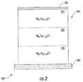
Fig. 2 is a schematic side elevation view of the UV photodetector ofFig. 1 , showing a compositionally graded magnesium-zinc oxide film having layers with different magnesium-to-zinc ratios; -
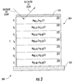
Fig. 3 is schematic side elevation view of an embodiment of a UV photodetector according to an embodiment, showing seven layers having seven magnesium-zinc oxide layers, each layer having a composition with a magnesium-to-zinc ratio that is different than the magnesium to zinc ratio of the other layers; and -
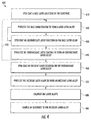
Fig. 4 is a method of making a compositionally graded UV photodetector using solutions that have different ratios of magnesium to zinc therein. - Reference will now be made to the drawings wherein like reference numerals identify similar structural features or aspects of the subject disclosure. For purposes of explanation and illustration, and not limitation, a partial view of an exemplary embodiment of an ultraviolet (UV) photodetector in accordance with the disclosure is shown in
Fig. 1 and is designated generally byreference character 100. Other embodiments of UV photodetectors and methods of making UV photodetectors in accordance with the disclosure, or aspects thereof, are provided inFigs. 2-4 , as will be described. The systems and methods described herein can be used for making UV sensors for flame detectors, such as for residential and/or industrial applications. - Referring now to
Fig. 1 UV photodetector 100 is shown.UV photodetector 100 includes afilm 104 deposited over asubstrate 102 and anelectrode 110. Electrode 110 is coupled tosubstrate 102 byfilm 104 and is connected electrically tofilm 104.Electrode 110 may include one or more electrode structures separated by one another by a gap (not shown for clarity reasons) that facilitates UV radiation received by the photodetector to contactfilm 104. -
Film 104 includes a magnesium-zinc oxide composition 106 that is compositionally graded such that zinc content in the film increases with distance from asurface 108 ofsubstrate 102. As indicated with the arrow appearing on the right-hand side ofFig. 1 , magnesium content infilm 104 decreases with distance fromsubstrate surface 108 and towardelectrode 110 from a film lower portion A to a film upper portion B. As indicated with the arrow appearing on the left-hand side ofFig. 1 , zinc content increases withinfilm 104 with distance fromsubstrate surface 108 and towardelectrode 110 from film lower portion A to film upper portion B. It is contemplated that compositional grading throughfilm 104 is such that the peak absorption of the film is red-shifted, i.e. shifted toward the visible portion of the electromagnetic spectrum, relative to magnesium-zinc oxide layers having a composition according to Mg0.8Zn0.2O. Red-shiftingfilm 104 compensates for the magnitude of the blue-shift associated certain types magnesium-zinc oxide films that can cause such films to have peak absorptions at wavelengths unsuitable for some applications. - With reference to
Fig. 2 , aphotodetector 200 is shown.Photodetector 200 is similar to thephotodetector 100 and additionally includes afilm 204 having plurality of layers deposited over asubstrate 202. In thisrespect film 204 includes abase layer 220overlaying substrate 202, one moreintermediate layers 222overlaying base layer 220, and anincident layer 224 overlaying the one or moreintermediate layer 222. Each ofbase layer 220,intermediate layer 222, andincident layer 224 has a magnesium-zinc oxide composition that is different from the other layers. - Within each layer the ratio of magnesium-to-zinc within the magnesium-zinc oxide is homogenous. Between layers, the ratio of magnesium-to-zinc in the magnesium-zinc oxide composition forming the respective layers is different from the others. For example, in the illustrated exemplary embodiments,
base layer 220 has a magnesium-zinc oxide composition according to the formula MgxZn(1-x)O,intermediate layer 222 has a magnesium-zinc oxide composition according to the formula MgyZn(1-y)O, andincident layer 224 has a magnesium-zinc oxide composition according to MgzZn(1-z)O where X is greater than Y and Y is greater than Z. In this respect layers closer to (i.e. proximate)substrate 202 have a greater ratio of magnesium-to-zinc than layers further from (i.e. distal)substrate 202. - With reference to
Fig. 3 , aUV photodetector 300 is shown according to an exemplary embodiment.UV photodetector 300 is similar tophotodetector 100 and additional includes a compositionally gradedfilm 304.Film 304 has seven layers formed from seven distinct magnesium-zinc oxide compositions.UV photodetector 300 has afirst layer 320overlaying substrate 302, asecond layer 322 overlayingfirst layer 320, and athird layer 324 overlayingsecond layer 322.UV photodetector 300 also includes afourth layer 326 overlayingthird layer 324, afifth layer 328 overlayingfourth layer 326, asixth layer 330 overlayingfifth layer 328, and aseventh layer 332 overlayingsixth layer 330.First layer 320 forms a base layer,seventh layer 332 forms an incident layer, and second through sixth layers 322- 330 form a plurality of intermediate layers.Electrode 310overlays incident layer 332 andfilm 304 generally, and is electrically connected toincident layer 332.Incident layer 332 has magnesium-zinc oxide composition according to Mg0.5Zn0.5O. - Each of the layers forming a respective layer of
film 304 have a magnesium-to-zinc ratio that is different from that of the other layers. Starting fromfirst layer 320, composition of the magnesium-zinc oxide layers changes in a stepwise manner upwards throughfilm 304. Each succeeding layer has incrementally less magnesium and incrementally more zinc than the underlying layer. In the illustrated exemplary embodiment layer metal contents change stepwise in increments of about 0.05, i.e. by about 5%, relative to the preceding layer. This step size enables the film to start with abase layer 320 having composition that pyrolyzes with cubic crystalline structureadjacent substrate 302 and which may have a UV absorption that is less than ideal for certain applications, and end with anincident layer 332 that both has a cubic crystalline structure and which has a UV absorption more suitable than the base layer for the intended application. This intermediate layers, i.e. layers 322 -330, transfer the cubic crystalline structure upwards (relative to the substrate) through the film stack as the magnesium to zinc ratio is adjusted. As will be appreciated, the increment size between layers can be larger or smaller, as suitable for an intended application. As will also be appreciated, the composition of the incident can be more or less than a 1 to 1 ratio of magnesium to zinc. As will further be appreciated, there can be fewer or more intermediate layers in the film stack. - In the illustrated exemplary embodiment,
first layer 320 has a magnesium-zinc oxide composition according to Mg0.80Zn0.20O,second layer 322 has a magnesium-zinc oxide composition according to Mg0.75Zn0.25O, andthird layer 324 has a magnesium-zinc oxide composition according to Mg0.70Zn0.30O. Fourth layer 326 has a magnesium-zinc oxide composition according to Mg0.65Zn0.35O,fifth layer 328 has a magnesium-zinc oxide composition according to Mg60Zn0.40O,sixth layer 330 has a magnesium-zinc oxide composition according to Mg0.55Zn0.45O, andseventh layer 332 has a magnesium-zinc oxide according to Mg0.50Zn0.50O. - The exemplary compositional gradient illustrated in
Fig. 3 (a) employs a spin coating and pyrolyzing deposition process that is optimized for magnesium-zinc oxide layers with Mg0.80Zn0.20O composition, (b) provides a peak absorption in the range of 220-280 nanometers, and (c) provides a cubic structure throughoutfilm 304 that is solar blind. As will be appreciated, peak absorption in the range of 220 and 280 nanometers provides sensitivity to UV radiation emitted by flame. Moreover, since of thelayers forming film 304, i.e.first layer 320 throughseventh layer 332, have a thickness Tx that is each about fifty (50) nanometers,film 304 has a thickness that is about 350 nanometers. As will be appreciated by those skilled in the art in view of the present disclosure, other step increments, base layer compositions, thicknesses, and incident layer compositions are possible within the scope of the present disclosure. Other film thicknesses and layer thicknesses are also contemplated. - With reference to
Fig. 4 , amethod 400 of making a UV photodetector is shown.Method 400 includes spin coating a first solution having a first magnesium-to-zinc ratio over a substrate, as indicated withbox 410. This forms a base coating with a magnesium-to-zinc ratio corresponding the magnesium-to-zinc ratio of the first solution. The base coating then is pyrolyzed to form a base layer, e.g. base layer 204 (shown inFig. 2 ), having a cubic crystalline structure as shown withbox 420. The resulting base layer has magnesium rich composition, e.g. a composition according to about Mg0.79Zn0.21O or Mg0.80Zn0.20O. - A second solution having a second magnesium-to-zinc ratio is spin coated over the base layer, as shown with
box 430. The second solution is less magnesium rich than the first solution, and has a magnesium-to-zinc ratio that is less than that of the first solution. This forms an intermediate coating with a magnesium-to-zinc ratio corresponding to the magnesium-to-zinc ratio of the second solution. The intermediate coating is then pyrolyzed to form an intermediate layer, e.g. intermediate layer 222 (shown inFig. 2 ), having a cubic crystalline structure as shown withbox 440. This process continues with successive coatings formed with lower ratios of magnesium-to-zinc, e.g. in increments of about x=0.05 or other suitable increment size, to carry the cubic phase of the underlying layer into the succeeding overlaying layer, until a desired incident layer, e.g. incident layer 224 (shown inFig. 2 ), is realized, as shown withbox 450. If the intermediate layer is not sufficiently close to the desired ratio of the incident layer, e.g. respective ratios of magnesium and zinc are each within 5% of a one-to-one ratio, thenoperations box 460, and calcined, as shown withbox 470. This forms an incident layer with a magnesium-to-zinc ratio of about 0.5 to 0.5 and which has a crystalline structure corresponding to that of the base layer, i.e. substantially cubic. - As used herein, pyrolysis means heating the coating to a predetermined temperature such that substantially all the organic ligands and solvents are driven off and/or oxidized (burned off), but not so much that the crystalline structure within the layer fully develops. This allows a layer subsequently deposited on the layer to both chemically bond with the layer and be influenced structurally by the crystalline structure of the pyrolyzed layer. Hence, the cubic structure not that the composition of the incident layer ordinarily precludes is transferred into the layer through the intervening layers from the base layer, which has a composition amenable to developing a cubic structure.
- Optionally, the film stack may be calcined, as shown with
box 480. Calcining may be done once the incident layer has been deposited over the one or more intervening layers, as shown with box 482. Calcining can be done at a predetermined calcination temperature that, as shown with box 484, may be higher than one or more of the predetermined pyrolysis temperatures used with the base layer and/or intermediate layer(s). Whether or not the optional calcining is done can be based on a determination of film stack performance subsequent to pyrolyzing the spin coated solution. - Magnesium-zinc oxide layers with compositions according to MgxZn(1-x)O can be formed by coating substrates with a magnesium and zinc solution and pyrolyzing the coating formed by the solution. This process can produce magnesium-zinc oxide film that has cubic crystalline structure and has a thickness that is on the order of about 350 nanometers. While generally satisfactory for their intended purpose, such materials can have a peak absorption of about 185 nanometers - which may require shifting in order for the magnesium-zinc oxide layer to benefit certain types of UV photodetectors like residential flame detectors, where peak absorptions of between 220 and 280 nanometers can be beneficial.
- One approach to shifting the peak absorption of the magnesium-zinc oxide layer is to shift the magnesium-to-zinc ratio layer to a ratio range between Mg0.36Zn0.64O and Mg0.62Zn0.38O, i.e. from x=0.36 to 0.62. However, magnesium-zinc oxide layers formed using conventional spin coat techniques with magnesium-to-zinc ratios may not yield a cubic crystalline structure, potentially reducing the solar blindness of magnesium-zinc layer.
- In embodiments described herein, photodetectors include compositionally graded layers of magnesium-zinc oxide compositions. The initial layer has a cubic crystalline structure that renders the layer solar blind and which may have a peak absorption wavelength too short for some types of flame detection. Intervening layers have magnesium-to-zinc ratios that decrease progressively, red shifting the peak absorption of the film stack to a wavelength suitable for flame detection, and have cubic crystalline structures owing to the influence of the crystalline structure of their respective underlying layer, thereby also being solar blind. As a result, the incident layer of the film stack has improved solar blindness due to the cubic crystalline microstructure of the layer and has a peak absorption wavelength suitable for flame detection due to the magnesium to zinc ratio of the magnesium-zinc oxide composition forming the layer.
- In certain embodiments, seven layers are deposited on a substrate by successively spin coating and pyrolyzing magnesium and zinc solution with different magnesium and zinc ratios. These different magnesium and zinc ratios pyrolyze as magnesium-zinc oxide compositions with ratios of zinc to magnesium that increase, layer wise, upwards (relative to the substrate) in the layer stack. Respective layers can have substantially the same thicknesses, e.g. about fifty (50), though different thicknesses are also contemplated. It is contemplated that the film have seven layers, each with a layer thickness of about fifty (50) nanometers, and that the film formed by the seven have a film thickness extending between the substrate and the top surface of the incident layer of about 350 nanometers.
- From a first layer pyrolyzed having a magnesium-to-zinc ratio that readily pyrolyzes into a cubic crystalline structure, successive layers with magnesium-to-zinc less apt to develop cubic crystalline structures on conventional substrates are deposited on magnesium-zinc oxide layers with cubic crystalline structures. The cubic crystalline structure of the underlying magnesium-zinc oxide layer causes the overlaying layer to develop a cubic crystalline structure - succeeding layers developing cubic crystalline structures through association with the cubic crystalline structure of the underlying layer. This allows the incident layer in the film to have a peak absorption in the range of 220 to 280 nanometers and have a cubic crystalline structure.
- Preferred embodiments of the present disclosure are set out below:
- 1. An ultraviolet (UV) photodetector, comprising:
- a substrate;
- an electrode coupled to the substrate; and
- a compositionally graded magnesium-zinc oxide film deposited on the substrate and connected to the electrode, wherein the film has a zinc content that increases from a portion of the film adjacent the substrate to a portion of the film opposite the substrate to red shift the peak absorption of the film.
- 2. A UV photodetector as recited in
claim 1, wherein the film includes a plurality of layers deposited on the substrate, each succeeding layer having a zinc content that is greater than each preceding layers interposed between the succeeding layer and the substrate. - 3. A UV photodetector as recited in
embodiment 1, wherein the film includes a plurality of layers deposited on the substrate, each succeeding layer having a magnesium content that is less than each of the preceding layers interposed between the succeeding layer and the substrate. - 4. A UV photodetector as recited in
embodiment 1, wherein the film comprises a plurality of layers having a cubic crystalline structure. - 5. A UV photodetector as recited in
embodiment 1, wherein the film has a thickness of between about 175 nanometers and about 350 nanometers. - 6. A UV photodetector as recited in
embodiment 1, wherein the film comprises a plurality of layers each having a thickness of between about twenty-five (25) nanometers and about fifty (50) nanometers. - 7. A UV photodetector as recited in
embodiment 1, wherein the film includes a base layer having magnesium-zinc oxide composition according to about Mg0.80Zn0.20O. - 8. A UV photodetector as recited in
embodiment 1, wherein the film includes an incident layer having a magnesium-zinc oxide composition with a magnesium to zinc ratio that is between 0.5 to 0.5 and 0.65 to 0.35. - 9. A UV photodetector as recited in
embodiment 1, wherein the film includes at least one intermediate layer overlaying the base layer and having less magnesium than the base layer. - 10. A UV photodetector as recited in
embodiment 1, wherein the film comprises:- a base layer with a MgxZn(1-x)O composition overlaying the substrate;
- one or more intermediate layers with a MgyZn(1-y)O composition overlaying the base layer; and
- an incident layer with a MgzZn(1-z)O composition overlaying the intermediate layer, wherein x is greater than y, and wherein y is greater than z.
- 11. A UV photodetector as recited in
embodiment 1, wherein the film comprises seven layers overlaying the substrate, wherein magnesium content decreases stepwise from a first layer adjacent the substrate through the seventh layer. - 12. A UV photodetector as recited in
embodiment 1, wherein the film comprises three or more layers overlaying the substrate, wherein zinc content increases stepwise from a first layer adjacent the substrate through the incident layer. - 13. A UV photodetector as recited in
embodiment 1, wherein the film has a peak absorption that is between about 220 nanometers and about 280 nanometers. - 14. An ultraviolet (UV) photodetector, comprising:
- a substrate;
- a film disposed on the substrate and connected to the electrodes, including:
- a first layer with a Mg0.80Zn0.20O composition overlaying the substrate;
- a second layer with a Mg0.75Zn0.25O composition overlaying the first layer;
- a third layer with a Mg0.70Zn0.30O composition overlaying the second layer;
- a fourth layer with a Mg0.65Zn0.35O composition overlaying the third layer;
- a fifth layer with a Mg0.60Zn0.40O composition overlaying the fourth layer;
- a sixth layer with a Mg0.55Zn0.45O composition overlaying the fifth layer; and
- a seventh layer with a Mg0.50Zn0.50O composition overlaying the sixth layer; and
- an electrode coupled to the substrate and connected to the film.
- 15. A method of making an ultraviolet (UV) photodetector, comprising:
- spin coating a base layer solution over a substrate;
- pyrolyzing the base layer solution to form a base layer;
- spin coating one or more intermediate layer solutions over the base layer; and
- pyrolyzing the one or more intermediate layer solution to form an intermediate layer, wherein the base layer solution includes magnesium and zinc in a ratio of Mgx and Zn(1-x), the one or more intermediate layer solutions includes magnesium and zinc in a ratio of Mgy and Zn(1-y), wherein x is greater than y.
- 16. A method as recited in embodiment 15, further including spin coating an incident layer solution over the one or more intermediate layers and pyrolyzing the incident layer solution to form an incident layer, wherein the incident layer has a magnesium-to-zinc ratio that is greater than a magnesium-to-zinc ratio of the one or more intermediate layers.
- 17. A method as recited in embodiment 17, further including calcining the base layer, the one ore more intermediate layers, and the incident layer.
- 18. A method as recited in embodiment 17, further including depositing an electrode over the incident layer.
- The methods and systems of the present disclosure, as described above and shown in the drawings, provide for UV photodetectors and methods of making such photodetectors with superior properties including compositionally tuned magnesium-zinc oxide layer for red shifting the spectrum of incident radiation wavelength absorbed by the photodetectors. While the apparatus and methods of the subject disclosure have been shown and described with reference to preferred embodiments, those skilled in the art will readily appreciate that changes and/or modifications may be made thereto without departing from the scope of the subject disclosure.
Claims (15)
- An ultraviolet (UV) photodetector, comprising:a substrate;an electrode coupled to the substrate; anda compositionally graded magnesium-zinc oxide film deposited on the substrate and connected to the electrode, wherein the film has a zinc content that increases from a portion of the film adjacent the substrate to a portion of the film opposite the substrate to red shift the peak absorption of the film.
- A UV photodetector as recited in claim 1, wherein the film includes a plurality of layers deposited on the substrate, each succeeding layer having a zinc content that is greater than each preceding layers interposed between the succeeding layer and the substrate, and/or each succeeding layer having a magnesium content that is less than each of the preceding layers interposed between the succeeding layer and the substrate.
- A UV photodetector as recited in claim 1 or claim 2, wherein the film comprises a plurality of layers having a cubic crystalline structure; and/or wherein the film has a thickness of between about 175 nanometers and about 350 nanometers.
- A UV photodetector as recited in any one of claims 1 to 3, wherein the film comprises a plurality of layers each having a thickness of between about twenty-five (25) nanometers and about fifty (50) nanometers.
- A UV photodetector as recited in any one of claims 1 to 4, wherein the film includes a base layer having magnesium-zinc oxide composition according to about Mg0.80Zn0.20O.
- A UV photodetector as recited in any one of claims 1 to 5, wherein the film includes an incident layer having a magnesium-zinc oxide composition with a magnesium to zinc ratio that is between 0.5 to 0.5 and 0.65 to 0.35.
- A UV photodetector as recited in any one of claims 1 to 6, wherein the film includes at least one intermediate layer overlaying the base layer and having less magnesium than the base layer.
- A UV photodetector as recited in any one of claims 1 to 7, wherein the film comprises:a base layer with a MgxZn(1-x)O composition overlaying the substrate;one or more intermediate layers with a MgyZn(1-y)O composition overlaying the base layer; andan incident layer with a MgzZn(1-z)O composition overlaying the intermediate layer, wherein x is greater than y, and wherein y is greater than z.
- A UV photodetector as recited in any one of claims 1 to 8, wherein the film comprises seven layers overlaying the substrate, wherein magnesium content decreases stepwise from a first layer adj acent the substrate through the seventh layer.
- A UV photodetector as recited in any one of claims 1 to 8, wherein the film comprises three or more layers overlaying the substrate, wherein zinc content increases stepwise from a first layer adj acent the substrate through the incident layer.
- A UV photodetector as recited in any one of claims 1 to 10, wherein the film has a peak absorption that is between about 220 nanometers and about 280 nanometers.
- A UV photodetector as recited in any one of claims 1 to 11, comprising:a substrate;a film disposed on the substrate and connected to the electrodes, including:a first layer with a Mg0.80Zn0.20O composition overlaying the substrate;a second layer with a Mg0.75Zn0.25O composition overlaying the first layer;a third layer with a Mg0.70Zn0.30O composition overlaying the second layer;a fourth layer with a Mg0.65Zn0.35O composition overlaying the third layer;a fifth layer with a Mg0.60Zn0.40O composition overlaying the fourth layer;a sixth layer with a Mg0.55Zn0.45O composition overlaying the fifth layer; anda seventh layer with a Mg0.50Zn0.50O composition overlaying the sixth layer; andan electrode coupled to the substrate and connected to the film.
- An ultraviolet (UV) photodetector, comprising:a substrate;a film disposed on the substrate and connected to the electrodes, including:a first layer with a Mg0.80Zn0.20O composition overlaying the substrate;a second layer with a Mg0.75Zn0.25O composition overlaying the first layer;a third layer with a Mg0.70Zn0.30O composition overlaying the second layer;a fourth layer with a Mg0.65Zn0.35O composition overlaying the third layer;a fifth layer with a Mg0.60Zn0.40O composition overlaying the fourth layer;a sixth layer with a Mg0.55Zn0.45O composition overlaying the fifth layer; anda seventh layer with a Mg0.50Zn0.50O composition overlaying the sixth layer; andan electrode coupled to the substrate and connected to the film.
- A method of making an ultraviolet (UV) photodetector, comprising:spin coating a base layer solution over a substrate;pyrolyzing the base layer solution to form a base layer;spin coating one or more intermediate layer solutions over the base layer; andpyrolyzing the one or more intermediate layer solution to form an intermediate layer, wherein the base layer solution includes magnesium and zinc in a ratio of Mgx and Zn(1-x), the one or more intermediate layer solutions includes magnesium and zinc in a ratio of Mgy and Zn(1-y), wherein x is greater than y.
- A method as recited in claim 14, further including spin coating an incident layer solution over the one or more intermediate layers and pyrolyzing the incident layer solution to form an incident layer, wherein the incident layer has a magnesium-to-zinc ratio that is greater than a magnesium-to-zinc ratio of the one or more intermediate layers;
optionally further including calcining the base layer, the one or more intermediate layers, and the incident layer, and/or depositing an electrode over the incident layer.
Priority Applications (1)
| Application Number | Priority Date | Filing Date | Title |
|---|---|---|---|
| EP19202486.7A EP3611768B1 (en) | 2015-07-28 | 2016-07-27 | Compositionally graded photodetectors |
Applications Claiming Priority (1)
| Application Number | Priority Date | Filing Date | Title |
|---|---|---|---|
| US201562198033P | 2015-07-28 | 2015-07-28 |
Related Child Applications (1)
| Application Number | Title | Priority Date | Filing Date |
|---|---|---|---|
| EP19202486.7A Division EP3611768B1 (en) | 2015-07-28 | 2016-07-27 | Compositionally graded photodetectors |
Publications (2)
| Publication Number | Publication Date |
|---|---|
| EP3125309A1 true EP3125309A1 (en) | 2017-02-01 |
| EP3125309B1 EP3125309B1 (en) | 2019-10-16 |
Family
ID=56801367
Family Applications (2)
| Application Number | Title | Priority Date | Filing Date |
|---|---|---|---|
| EP19202486.7A Active EP3611768B1 (en) | 2015-07-28 | 2016-07-27 | Compositionally graded photodetectors |
| EP16181490.0A Active EP3125309B1 (en) | 2015-07-28 | 2016-07-27 | Compositionally graded photodetectors |
Family Applications Before (1)
| Application Number | Title | Priority Date | Filing Date |
|---|---|---|---|
| EP19202486.7A Active EP3611768B1 (en) | 2015-07-28 | 2016-07-27 | Compositionally graded photodetectors |
Country Status (2)
| Country | Link |
|---|---|
| US (1) | US9806125B2 (en) |
| EP (2) | EP3611768B1 (en) |
Cited By (1)
| Publication number | Priority date | Publication date | Assignee | Title |
|---|---|---|---|---|
| EP4194592A4 (en) * | 2020-08-06 | 2024-08-21 | Shin-Etsu Chemical Co., Ltd. | Semiconductor laminate, semiconductor element, and method for producing semiconductor element |
Families Citing this family (2)
| Publication number | Priority date | Publication date | Assignee | Title |
|---|---|---|---|---|
| WO2012040299A2 (en) | 2010-09-22 | 2012-03-29 | First Solar, Inc | A thin-film photovoltaic device with a zinc magnesium oxide window layer |
| WO2018222528A1 (en) | 2017-05-30 | 2018-12-06 | Carrier Corporation | Semiconductor film and phototube light detector |
Citations (1)
| Publication number | Priority date | Publication date | Assignee | Title |
|---|---|---|---|---|
| JP2013004674A (en) * | 2011-06-15 | 2013-01-07 | Stanley Electric Co Ltd | Ultraviolet light-receiving element and manufacturing method therefor |
Family Cites Families (68)
| Publication number | Priority date | Publication date | Assignee | Title |
|---|---|---|---|---|
| JPS5272596A (en) | 1975-12-15 | 1977-06-17 | Yuwa Sangyo Kk | Composite early fire detecting system and device therefor |
| GB2222908A (en) | 1988-09-14 | 1990-03-21 | Haroon Ahmed | Sensor device |
| US5699035A (en) | 1991-12-13 | 1997-12-16 | Symetrix Corporation | ZnO thin-film varistors and method of making the same |
| US5339070A (en) | 1992-07-21 | 1994-08-16 | Srs Technologies | Combined UV/IR flame detection system |
| EP0646791B1 (en) | 1993-09-30 | 2001-09-05 | Nittan Company, Limited | Sensor device, and electronic equipment each having sensor device incorporated therein |
| US5494700A (en) | 1994-04-05 | 1996-02-27 | The Curators Of The University Of Missouri | Method of coating a substrate with a metal oxide film from an aqueous solution comprising a metal cation and a polymerizable organic solvent |
| US6064064A (en) | 1996-03-01 | 2000-05-16 | Fire Sentry Corporation | Fire detector |
| GB9805949D0 (en) | 1998-03-19 | 1998-05-20 | Thorn Security | A detector |
| US6166647A (en) | 2000-01-18 | 2000-12-26 | Jaesent Inc. | Fire detector |
| KR100343949B1 (en) | 2000-01-26 | 2002-07-24 | 한국과학기술연구원 | METHOD FOR FABRICATING ZnO THIN FILM FOR ULTRAVIOLET DETECTION AND EMISSION SOURCE OPERATED AT ROOM TEMPERATURE, AND APPARATUS THEREFOR |
| AU2001268756A1 (en) | 2000-06-26 | 2002-01-08 | University Of Maryland | Mgzno based uv detectors |
| US6621192B2 (en) | 2000-07-13 | 2003-09-16 | Rutgers, The State University Of New Jersey | Integrated tunable surface acoustic wave technology and sensors provided thereby |
| US6423983B1 (en) | 2000-10-13 | 2002-07-23 | North Carolina State University | Optoelectronic and microelectronic devices including cubic ZnMgO and/or CdMgO alloys |
| WO2003061020A1 (en) | 2002-01-04 | 2003-07-24 | Rutgers, The State University Of New Jersey | SCHOTTKY DIODE WITH SILVER LAYER CONTACTING THE ZnO AND MgxZn1-xO FILMS |
| CN1182593C (en) | 2002-08-05 | 2004-12-29 | 浙江大学 | Preparation method of zinc oxide ultraviolet photodetector prototype device |
| US7083880B2 (en) | 2002-08-15 | 2006-08-01 | Freescale Semiconductor, Inc. | Lithographic template and method of formation and use |
| US7172813B2 (en) | 2003-05-20 | 2007-02-06 | Burgener Ii Robert H | Zinc oxide crystal growth substrate |
| US7202794B2 (en) | 2004-07-20 | 2007-04-10 | General Monitors, Inc. | Flame detection system |
| SG124303A1 (en) | 2005-01-18 | 2006-08-30 | Agency Science Tech & Res | Thin films of ferroelectric materials and a methodfor preparing same |
| CN100358159C (en) | 2005-02-28 | 2007-12-26 | 浙江大学 | Thin film material for sunlight blind area ultraviolet detector and its producing method |
| JP5190570B2 (en) | 2005-03-28 | 2013-04-24 | 国立大学法人岩手大学 | Ultraviolet sensor element and manufacturing method thereof |
| US7333910B2 (en) | 2005-04-26 | 2008-02-19 | Semiconductor Energy Laboratory Co., Ltd. | Fire sensing method and fire sensing system using wireless chip for sensing fire |
| US7541938B1 (en) | 2006-03-29 | 2009-06-02 | Darell Eugene Engelhaupt | Optical flame detection system and method |
| US7566875B2 (en) | 2006-04-13 | 2009-07-28 | Integrated Micro Sensors Inc. | Single-chip monolithic dual-band visible- or solar-blind photodetector |
| US20080036593A1 (en) | 2006-08-04 | 2008-02-14 | The Government Of The Us, As Represented By The Secretary Of The Navy | Volume sensor: data fusion-based, multi-sensor system for advanced damage control |
| CN101210313A (en) | 2006-12-29 | 2008-07-02 | 中国科学院长春光学精密机械与物理研究所 | Method for growing MgxZn1-xO film by electron-beam evaporation |
| KR101009532B1 (en) | 2007-02-26 | 2011-01-18 | 주식회사 엘지화학 | Zinc oxide multilayer thin film and method for manufacturing same |
| US7767253B2 (en) | 2007-03-09 | 2010-08-03 | Guardian Industries Corp. | Method of making a photovoltaic device with antireflective coating |
| CN100561742C (en) | 2007-04-30 | 2009-11-18 | 西安交通大学 | Back-illuminated ZnO-based solid-state focal plane detector array for ultraviolet imaging and its fabrication |
| GB0718299D0 (en) | 2007-09-19 | 2007-10-31 | Univ Bristol | Gas sensor |
| CN101285147B (en) | 2008-06-04 | 2010-11-10 | 中国科学院长春光学精密机械与物理研究所 | Method for preparing MgxZn1-xO semiconductor alloy body material with single cubic phase structure |
| CN101285173A (en) | 2008-06-04 | 2008-10-15 | 长春理工大学 | Double-target radio frequency magnetron cosputtering method of Mg<x>Zn<1-x>O film |
| CN101286535A (en) | 2008-06-04 | 2008-10-15 | 长春理工大学 | Sun blind region ultraviolet detector with pn junction MgxZn1-xO film |
| US8926317B2 (en) | 2008-12-15 | 2015-01-06 | Exxonmobil Research And Engineering Company | System and method for controlling fired heater operations |
| WO2010069353A1 (en) | 2008-12-19 | 2010-06-24 | Minimax Gmbh & Co. Kg | Method and device for the early detection of fires |
| US8536618B2 (en) | 2009-11-03 | 2013-09-17 | The Regents Of The University Of California | Light emitting diode structure utilizing zinc oxide nanorod arrays on one or more surfaces, and a low cost method of producing such zinc oxide nanorod arrays |
| JP5275950B2 (en) | 2009-05-01 | 2013-08-28 | 富士フイルム株式会社 | Laminated film and manufacturing method thereof, photoelectric conversion element and manufacturing method thereof, and solar cell |
| CN101807619B (en) | 2010-03-19 | 2012-02-01 | 河南大学 | A kind of transparent flexible ultraviolet detector and preparation method thereof |
| CN101866983B (en) | 2010-05-10 | 2014-09-03 | 北京交通大学 | Manufacturing method of fast response UV detector of n-type doped ZnO thin film |
| WO2011162127A1 (en) | 2010-06-21 | 2011-12-29 | 株式会社 村田製作所 | Ultraviolet sensor and method for manufacturing ultraviolet sensor |
| US8547238B2 (en) | 2010-06-30 | 2013-10-01 | Knowflame, Inc. | Optically redundant fire detector for false alarm rejection |
| CN101969023B (en) | 2010-08-04 | 2012-05-02 | 长春理工大学 | Method for making step growth MgxZn1-xO thin film on silicon substrate |
| CN101935876A (en) | 2010-09-14 | 2011-01-05 | 浙江大学 | A kind of In-doped ZnO monodisperse nanoparticles and its synthesis method |
| CN102110735B (en) | 2010-10-13 | 2012-09-26 | 兰州大学 | Semiconductor ultraviolet detection sensor and preparation method thereof |
| CN201964955U (en) | 2010-12-31 | 2011-09-07 | 上海神明控制工程有限公司 | Ultraviolet flame-detecting probe |
| KR101192934B1 (en) | 2011-02-28 | 2012-10-18 | 성균관대학교산학협력단 | Ultraviolet detector with metal oxide nanostructures and fire monitoring apparatus using ultraviolet detector with metal oxide nanostructures |
| JP5445989B2 (en) | 2011-03-09 | 2014-03-19 | 株式会社村田製作所 | Ultraviolet sensor and method for manufacturing ultraviolet sensor |
| CN102694053B (en) | 2011-03-22 | 2015-08-05 | 中国科学院微电子研究所 | Semiconductor device and manufacturing method thereof |
| US8878157B2 (en) | 2011-10-20 | 2014-11-04 | University Of Kansas | Semiconductor-graphene hybrids formed using solution growth |
| JP6188711B2 (en) | 2011-12-01 | 2017-08-30 | ザ ユニバーシティ オブ ユタ リサーチ ファウンデイション | Photonic element on flat and curved substrate and method of manufacturing the same |
| CN102569483A (en) | 2011-12-19 | 2012-07-11 | 北京交通大学 | MgZnO solar-blind photoresistor and preparation method thereof |
| CN202633358U (en) | 2011-12-22 | 2012-12-26 | 安徽康蓝光电股份有限公司 | Ultraviolet-visible photoelectric detector with quantum dot structure |
| JP2014011310A (en) | 2012-06-29 | 2014-01-20 | Toyota Motor Corp | Method for manufacturing semiconductor film |
| CN103205706B (en) | 2013-03-08 | 2015-11-18 | 深圳大学 | A kind of preparation method of cubic structure MgZnO film |
| US9112074B2 (en) | 2013-03-22 | 2015-08-18 | University Of Central Florida Research Foundation, Inc. | UV photodetectors having semiconductor metal oxide layer |
| CN103219418B (en) | 2013-03-26 | 2016-07-27 | 华中科技大学 | A kind of ultraviolet light detector with nano heterogeneous composite construction and preparation method thereof |
| US9423295B2 (en) | 2013-04-24 | 2016-08-23 | Agency For Science, Technology And Research | Photo-sensor with a transparent substrate and an in-plane electrode pair |
| CN103258869A (en) | 2013-05-07 | 2013-08-21 | 哈尔滨工业大学 | Ultraviolet and infrared double-color detector based on zinc oxide materials and manufacturing method thereof |
| CN103346171B (en) | 2013-05-31 | 2016-04-27 | 西安交通大学 | A kind of response enhancement type ZnO based photoconduction detector and preparation method thereof |
| CN103441154B (en) | 2013-06-26 | 2015-08-12 | 北京科技大学 | A kind of ZnO nanometer array ultraviolet detector and preparation method thereof |
| CN103346199B (en) | 2013-07-10 | 2015-09-16 | 合肥工业大学 | Based on the UV photodetector and preparation method thereof of single-layer graphene/nanometic zinc oxide rod array schottky junction |
| JP2015023053A (en) | 2013-07-16 | 2015-02-02 | 株式会社リコー | Electromechanical conversion element, droplet discharge head, droplet discharge apparatus, image forming apparatus, and method of manufacturing electromechanical conversion element |
| CN103441186B (en) | 2013-08-29 | 2016-04-06 | 江苏大学 | A kind of preparation method of ultraviolet detector |
| CN103545397B (en) | 2013-10-29 | 2016-02-24 | 中国科学院化学研究所 | Thin film ultraviolet detector and preparation method thereof and application |
| CN103915524A (en) | 2014-04-03 | 2014-07-09 | 浙江大学 | Self-driven ZnO-based ultraviolet detector and manufacturing method thereof |
| CN103972310B (en) | 2014-04-30 | 2016-04-27 | 中国科学院长春光学精密机械与物理研究所 | A kind of preparation method of zinc oxide based p type material |
| CN104504838A (en) | 2014-12-15 | 2015-04-08 | 长春理工大学 | Ultraviolet flame detector adopting zinc oxide-based semiconductor film |
| CN104617180B (en) | 2015-01-16 | 2018-01-09 | 浙江大学 | A kind of graphene/boron nitride/zinc oxide ultraviolet detector and preparation method thereof |
-
2016
- 2016-07-20 US US15/215,085 patent/US9806125B2/en active Active
- 2016-07-27 EP EP19202486.7A patent/EP3611768B1/en active Active
- 2016-07-27 EP EP16181490.0A patent/EP3125309B1/en active Active
Patent Citations (1)
| Publication number | Priority date | Publication date | Assignee | Title |
|---|---|---|---|---|
| JP2013004674A (en) * | 2011-06-15 | 2013-01-07 | Stanley Electric Co Ltd | Ultraviolet light-receiving element and manufacturing method therefor |
Non-Patent Citations (2)
| Title |
|---|
| HOGGAS K ET AL: "Structural, microstructural, and optical properties of Zn1-xMgxO thin films grown onto glass substrate by ultrasonic spray pyrol", APPLIED PHYSICS A MATERIALS SCIENCE & PROCESSING, SPRINGER BERLIN HEIDELBERG, BERLIN/HEIDELBERG, vol. 120, no. 2, 28 May 2015 (2015-05-28), pages 745 - 755, XP035516320, ISSN: 0947-8396, [retrieved on 20150528], DOI: 10.1007/S00339-015-9252-7 * |
| Y. N. HOU ET AL: "Monolithic color-selective ultraviolet (266-315?nm) photodetector based on a wurtzite MgxZn1-xO film", APPLIED PHYSICS LETTERS, vol. 105, no. 13, 29 September 2014 (2014-09-29), US, pages 133510, XP055329261, ISSN: 0003-6951, DOI: 10.1063/1.4897300 * |
Cited By (2)
| Publication number | Priority date | Publication date | Assignee | Title |
|---|---|---|---|---|
| EP4194592A4 (en) * | 2020-08-06 | 2024-08-21 | Shin-Etsu Chemical Co., Ltd. | Semiconductor laminate, semiconductor element, and method for producing semiconductor element |
| US12593625B2 (en) | 2020-08-06 | 2026-03-31 | Shin-Etsu Chemical Co., Ltd. | Semiconductor laminate, semiconductor device, and method for manufacturing semiconductor device |
Also Published As
| Publication number | Publication date |
|---|---|
| US20170033150A1 (en) | 2017-02-02 |
| EP3125309B1 (en) | 2019-10-16 |
| US9806125B2 (en) | 2017-10-31 |
| EP3611768A1 (en) | 2020-02-19 |
| EP3611768B1 (en) | 2022-08-31 |
Similar Documents
| Publication | Publication Date | Title |
|---|---|---|
| Pati et al. | Role of oxygen vacancy in optical and gas sensing characteristics of ZnO thin films | |
| de Castro et al. | Vanadium oxide thin films produced by magnetron sputtering from a V2O5 target at room temperature | |
| Dan et al. | Enhancing spectrally selective response of W/WAlN/WAlON/Al2O3–based nanostructured multilayer absorber coating through graded optical constants | |
| EP3611768B1 (en) | Compositionally graded photodetectors | |
| Zhao et al. | Avalanche effect and high external quantum efficiency in MgZnO/Au/ZnO sandwich structure photodetector | |
| Manjula et al. | Sensing characteristics of nanocrystalline bismuth oxide clad-modified fiber optic gas sensor | |
| Singh et al. | Fabrication and characterization of Al: ZnO based MSM ultraviolet photodetectors | |
| Tesfamichael et al. | The effect of pressure and W-doping on the properties of ZnO thin films for NO2 gas sensing | |
| Taylor et al. | The electrical, optical and structural properties of In x Zn1− x O y (0⩽ x⩽ 1) thin films by combinatorial techniques | |
| Shewale et al. | UV sensitive pulsed laser deposited ZnO thin films: Influence of growth temperature | |
| Sankarasubramanian et al. | Structural, optical and electrical properties of transparent conducting hydrophobic cadmium oxide thin films prepared by spray pyrolysis technique | |
| Jagtap et al. | Low temperature amorphous growth of semiconducting Y–Ba–Cu–O oxide thin films in view of infrared bolometric detection | |
| Lei et al. | Mid-wave interband cascade infrared photodetectors based on GaInAsSb absorbers | |
| KR20180135122A (en) | Metal substrate | |
| Ouadfel et al. | Silicon carbide thin films with different processing growth as an alternative for energetic application | |
| EP2427587A1 (en) | Layer system having barrier properties and a structured conductive layer, method for producing the same, and use of such a layer system | |
| Hernandez-Como et al. | Low-temperature processed ZnO and CdS photodetectors deposited by pulsed laser deposition | |
| Chakraborty et al. | Air-annealed growth and characterization of Cd1-xZnxTe thin films grown from CdTe/ZnTe/CdTe multi-stacks | |
| Bueno et al. | Luminescence of Eu3+ in the thin film heterojunction GaAs/SnO2 | |
| Hasan et al. | Analysis of the optical absorption characteristics of CuInSe2 thin films | |
| Warwick et al. | On the effects of electric fields in aerosol assisted chemical vapour deposition reactions of vanadyl acetylacetonate solutions in ethanol | |
| US11217720B2 (en) | Method for depositing a CdTe layer on a substrate | |
| Marotta et al. | Electrical and optical characterization of multilayered thin film based on pulsed laser deposition of metal oxides | |
| KR20200097931A (en) | Broadband photodetector and manufacturing method thereof | |
| Wan et al. | TiN x O y transparent electrode material for HgCdTe infrared devices |
Legal Events
| Date | Code | Title | Description |
|---|---|---|---|
| PUAI | Public reference made under article 153(3) epc to a published international application that has entered the european phase |
Free format text: ORIGINAL CODE: 0009012 |
|
| STAA | Information on the status of an ep patent application or granted ep patent |
Free format text: STATUS: THE APPLICATION HAS BEEN PUBLISHED |
|
| AK | Designated contracting states |
Kind code of ref document: A1 Designated state(s): AL AT BE BG CH CY CZ DE DK EE ES FI FR GB GR HR HU IE IS IT LI LT LU LV MC MK MT NL NO PL PT RO RS SE SI SK SM TR |
|
| AX | Request for extension of the european patent |
Extension state: BA ME |
|
| STAA | Information on the status of an ep patent application or granted ep patent |
Free format text: STATUS: REQUEST FOR EXAMINATION WAS MADE |
|
| 17P | Request for examination filed |
Effective date: 20170725 |
|
| RBV | Designated contracting states (corrected) |
Designated state(s): AL AT BE BG CH CY CZ DE DK EE ES FI FR GB GR HR HU IE IS IT LI LT LU LV MC MK MT NL NO PL PT RO RS SE SI SK SM TR |
|
| GRAP | Despatch of communication of intention to grant a patent |
Free format text: ORIGINAL CODE: EPIDOSNIGR1 |
|
| STAA | Information on the status of an ep patent application or granted ep patent |
Free format text: STATUS: GRANT OF PATENT IS INTENDED |
|
| INTG | Intention to grant announced |
Effective date: 20181108 |
|
| GRAJ | Information related to disapproval of communication of intention to grant by the applicant or resumption of examination proceedings by the epo deleted |
Free format text: ORIGINAL CODE: EPIDOSDIGR1 |
|
| STAA | Information on the status of an ep patent application or granted ep patent |
Free format text: STATUS: REQUEST FOR EXAMINATION WAS MADE |
|
| GRAP | Despatch of communication of intention to grant a patent |
Free format text: ORIGINAL CODE: EPIDOSNIGR1 |
|
| INTC | Intention to grant announced (deleted) | ||
| STAA | Information on the status of an ep patent application or granted ep patent |
Free format text: STATUS: GRANT OF PATENT IS INTENDED |
|
| INTG | Intention to grant announced |
Effective date: 20190425 |
|
| GRAS | Grant fee paid |
Free format text: ORIGINAL CODE: EPIDOSNIGR3 |
|
| GRAA | (expected) grant |
Free format text: ORIGINAL CODE: 0009210 |
|
| STAA | Information on the status of an ep patent application or granted ep patent |
Free format text: STATUS: THE PATENT HAS BEEN GRANTED |
|
| AK | Designated contracting states |
Kind code of ref document: B1 Designated state(s): AL AT BE BG CH CY CZ DE DK EE ES FI FR GB GR HR HU IE IS IT LI LT LU LV MC MK MT NL NO PL PT RO RS SE SI SK SM TR |
|
| REG | Reference to a national code |
Ref country code: GB Ref legal event code: FG4D |
|
| REG | Reference to a national code |
Ref country code: CH Ref legal event code: EP |
|
| REG | Reference to a national code |
Ref country code: DE Ref legal event code: R096 Ref document number: 602016022465 Country of ref document: DE |
|
| REG | Reference to a national code |
Ref country code: IE Ref legal event code: FG4D |
|
| REG | Reference to a national code |
Ref country code: AT Ref legal event code: REF Ref document number: 1192144 Country of ref document: AT Kind code of ref document: T Effective date: 20191115 |
|
| REG | Reference to a national code |
Ref country code: NL Ref legal event code: MP Effective date: 20191016 |
|
| REG | Reference to a national code |
Ref country code: LT Ref legal event code: MG4D |
|
| REG | Reference to a national code |
Ref country code: AT Ref legal event code: MK05 Ref document number: 1192144 Country of ref document: AT Kind code of ref document: T Effective date: 20191016 |
|
| PG25 | Lapsed in a contracting state [announced via postgrant information from national office to epo] |
Ref country code: PT Free format text: LAPSE BECAUSE OF FAILURE TO SUBMIT A TRANSLATION OF THE DESCRIPTION OR TO PAY THE FEE WITHIN THE PRESCRIBED TIME-LIMIT Effective date: 20200217 Ref country code: SE Free format text: LAPSE BECAUSE OF FAILURE TO SUBMIT A TRANSLATION OF THE DESCRIPTION OR TO PAY THE FEE WITHIN THE PRESCRIBED TIME-LIMIT Effective date: 20191016 Ref country code: LV Free format text: LAPSE BECAUSE OF FAILURE TO SUBMIT A TRANSLATION OF THE DESCRIPTION OR TO PAY THE FEE WITHIN THE PRESCRIBED TIME-LIMIT Effective date: 20191016 Ref country code: BG Free format text: LAPSE BECAUSE OF FAILURE TO SUBMIT A TRANSLATION OF THE DESCRIPTION OR TO PAY THE FEE WITHIN THE PRESCRIBED TIME-LIMIT Effective date: 20200116 Ref country code: FI Free format text: LAPSE BECAUSE OF FAILURE TO SUBMIT A TRANSLATION OF THE DESCRIPTION OR TO PAY THE FEE WITHIN THE PRESCRIBED TIME-LIMIT Effective date: 20191016 Ref country code: PL Free format text: LAPSE BECAUSE OF FAILURE TO SUBMIT A TRANSLATION OF THE DESCRIPTION OR TO PAY THE FEE WITHIN THE PRESCRIBED TIME-LIMIT Effective date: 20191016 Ref country code: LT Free format text: LAPSE BECAUSE OF FAILURE TO SUBMIT A TRANSLATION OF THE DESCRIPTION OR TO PAY THE FEE WITHIN THE PRESCRIBED TIME-LIMIT Effective date: 20191016 Ref country code: GR Free format text: LAPSE BECAUSE OF FAILURE TO SUBMIT A TRANSLATION OF THE DESCRIPTION OR TO PAY THE FEE WITHIN THE PRESCRIBED TIME-LIMIT Effective date: 20200117 Ref country code: NO Free format text: LAPSE BECAUSE OF FAILURE TO SUBMIT A TRANSLATION OF THE DESCRIPTION OR TO PAY THE FEE WITHIN THE PRESCRIBED TIME-LIMIT Effective date: 20200116 Ref country code: AT Free format text: LAPSE BECAUSE OF FAILURE TO SUBMIT A TRANSLATION OF THE DESCRIPTION OR TO PAY THE FEE WITHIN THE PRESCRIBED TIME-LIMIT Effective date: 20191016 Ref country code: NL Free format text: LAPSE BECAUSE OF FAILURE TO SUBMIT A TRANSLATION OF THE DESCRIPTION OR TO PAY THE FEE WITHIN THE PRESCRIBED TIME-LIMIT Effective date: 20191016 |
|
| PG25 | Lapsed in a contracting state [announced via postgrant information from national office to epo] |
Ref country code: HR Free format text: LAPSE BECAUSE OF FAILURE TO SUBMIT A TRANSLATION OF THE DESCRIPTION OR TO PAY THE FEE WITHIN THE PRESCRIBED TIME-LIMIT Effective date: 20191016 Ref country code: IS Free format text: LAPSE BECAUSE OF FAILURE TO SUBMIT A TRANSLATION OF THE DESCRIPTION OR TO PAY THE FEE WITHIN THE PRESCRIBED TIME-LIMIT Effective date: 20200224 Ref country code: RS Free format text: LAPSE BECAUSE OF FAILURE TO SUBMIT A TRANSLATION OF THE DESCRIPTION OR TO PAY THE FEE WITHIN THE PRESCRIBED TIME-LIMIT Effective date: 20191016 |
|
| PG25 | Lapsed in a contracting state [announced via postgrant information from national office to epo] |
Ref country code: AL Free format text: LAPSE BECAUSE OF FAILURE TO SUBMIT A TRANSLATION OF THE DESCRIPTION OR TO PAY THE FEE WITHIN THE PRESCRIBED TIME-LIMIT Effective date: 20191016 |
|
| REG | Reference to a national code |
Ref country code: DE Ref legal event code: R097 Ref document number: 602016022465 Country of ref document: DE |
|
| PG2D | Information on lapse in contracting state deleted |
Ref country code: IS |
|
| PG25 | Lapsed in a contracting state [announced via postgrant information from national office to epo] |
Ref country code: EE Free format text: LAPSE BECAUSE OF FAILURE TO SUBMIT A TRANSLATION OF THE DESCRIPTION OR TO PAY THE FEE WITHIN THE PRESCRIBED TIME-LIMIT Effective date: 20191016 Ref country code: DK Free format text: LAPSE BECAUSE OF FAILURE TO SUBMIT A TRANSLATION OF THE DESCRIPTION OR TO PAY THE FEE WITHIN THE PRESCRIBED TIME-LIMIT Effective date: 20191016 Ref country code: RO Free format text: LAPSE BECAUSE OF FAILURE TO SUBMIT A TRANSLATION OF THE DESCRIPTION OR TO PAY THE FEE WITHIN THE PRESCRIBED TIME-LIMIT Effective date: 20191016 Ref country code: CZ Free format text: LAPSE BECAUSE OF FAILURE TO SUBMIT A TRANSLATION OF THE DESCRIPTION OR TO PAY THE FEE WITHIN THE PRESCRIBED TIME-LIMIT Effective date: 20191016 Ref country code: ES Free format text: LAPSE BECAUSE OF FAILURE TO SUBMIT A TRANSLATION OF THE DESCRIPTION OR TO PAY THE FEE WITHIN THE PRESCRIBED TIME-LIMIT Effective date: 20191016 Ref country code: IS Free format text: LAPSE BECAUSE OF FAILURE TO SUBMIT A TRANSLATION OF THE DESCRIPTION OR TO PAY THE FEE WITHIN THE PRESCRIBED TIME-LIMIT Effective date: 20200216 |
|
| PLBE | No opposition filed within time limit |
Free format text: ORIGINAL CODE: 0009261 |
|
| STAA | Information on the status of an ep patent application or granted ep patent |
Free format text: STATUS: NO OPPOSITION FILED WITHIN TIME LIMIT |
|
| PG25 | Lapsed in a contracting state [announced via postgrant information from national office to epo] |
Ref country code: SM Free format text: LAPSE BECAUSE OF FAILURE TO SUBMIT A TRANSLATION OF THE DESCRIPTION OR TO PAY THE FEE WITHIN THE PRESCRIBED TIME-LIMIT Effective date: 20191016 Ref country code: IT Free format text: LAPSE BECAUSE OF FAILURE TO SUBMIT A TRANSLATION OF THE DESCRIPTION OR TO PAY THE FEE WITHIN THE PRESCRIBED TIME-LIMIT Effective date: 20191016 Ref country code: SK Free format text: LAPSE BECAUSE OF FAILURE TO SUBMIT A TRANSLATION OF THE DESCRIPTION OR TO PAY THE FEE WITHIN THE PRESCRIBED TIME-LIMIT Effective date: 20191016 |
|
| 26N | No opposition filed |
Effective date: 20200717 |
|
| PG25 | Lapsed in a contracting state [announced via postgrant information from national office to epo] |
Ref country code: SI Free format text: LAPSE BECAUSE OF FAILURE TO SUBMIT A TRANSLATION OF THE DESCRIPTION OR TO PAY THE FEE WITHIN THE PRESCRIBED TIME-LIMIT Effective date: 20191016 |
|
| PG25 | Lapsed in a contracting state [announced via postgrant information from national office to epo] |
Ref country code: MC Free format text: LAPSE BECAUSE OF FAILURE TO SUBMIT A TRANSLATION OF THE DESCRIPTION OR TO PAY THE FEE WITHIN THE PRESCRIBED TIME-LIMIT Effective date: 20191016 |
|
| REG | Reference to a national code |
Ref country code: CH Ref legal event code: PL |
|
| REG | Reference to a national code |
Ref country code: BE Ref legal event code: MM Effective date: 20200731 |
|
| PG25 | Lapsed in a contracting state [announced via postgrant information from national office to epo] |
Ref country code: FR Free format text: LAPSE BECAUSE OF NON-PAYMENT OF DUE FEES Effective date: 20200731 Ref country code: CH Free format text: LAPSE BECAUSE OF NON-PAYMENT OF DUE FEES Effective date: 20200731 Ref country code: LU Free format text: LAPSE BECAUSE OF NON-PAYMENT OF DUE FEES Effective date: 20200727 Ref country code: LI Free format text: LAPSE BECAUSE OF NON-PAYMENT OF DUE FEES Effective date: 20200731 |
|
| PG25 | Lapsed in a contracting state [announced via postgrant information from national office to epo] |
Ref country code: BE Free format text: LAPSE BECAUSE OF NON-PAYMENT OF DUE FEES Effective date: 20200731 |
|
| PG25 | Lapsed in a contracting state [announced via postgrant information from national office to epo] |
Ref country code: IE Free format text: LAPSE BECAUSE OF NON-PAYMENT OF DUE FEES Effective date: 20200727 |
|
| PG25 | Lapsed in a contracting state [announced via postgrant information from national office to epo] |
Ref country code: TR Free format text: LAPSE BECAUSE OF FAILURE TO SUBMIT A TRANSLATION OF THE DESCRIPTION OR TO PAY THE FEE WITHIN THE PRESCRIBED TIME-LIMIT Effective date: 20191016 Ref country code: MT Free format text: LAPSE BECAUSE OF FAILURE TO SUBMIT A TRANSLATION OF THE DESCRIPTION OR TO PAY THE FEE WITHIN THE PRESCRIBED TIME-LIMIT Effective date: 20191016 Ref country code: CY Free format text: LAPSE BECAUSE OF FAILURE TO SUBMIT A TRANSLATION OF THE DESCRIPTION OR TO PAY THE FEE WITHIN THE PRESCRIBED TIME-LIMIT Effective date: 20191016 |
|
| PG25 | Lapsed in a contracting state [announced via postgrant information from national office to epo] |
Ref country code: MK Free format text: LAPSE BECAUSE OF FAILURE TO SUBMIT A TRANSLATION OF THE DESCRIPTION OR TO PAY THE FEE WITHIN THE PRESCRIBED TIME-LIMIT Effective date: 20191016 |
|
| REG | Reference to a national code |
Ref country code: DE Ref legal event code: R079 Ref document number: 602016022465 Country of ref document: DE Free format text: PREVIOUS MAIN CLASS: H01L0031090000 Ipc: H10F0030100000 |
|
| PGFP | Annual fee paid to national office [announced via postgrant information from national office to epo] |
Ref country code: GB Payment date: 20250619 Year of fee payment: 10 |
|
| PGFP | Annual fee paid to national office [announced via postgrant information from national office to epo] |
Ref country code: DE Payment date: 20250620 Year of fee payment: 10 |
|
| REG | Reference to a national code |
Ref country code: DE Ref legal event code: R081 Ref document number: 602016022465 Country of ref document: DE Owner name: DETECTOR ELECTRONICS BUYER US, LLC, BLOOMINGTO, US Free format text: FORMER OWNER: CARRIER CORPORATION, FARMINGTON, CONN., US |
|
| REG | Reference to a national code |
Ref country code: GB Ref legal event code: 732E Free format text: REGISTERED BETWEEN 20260305 AND 20260311 |