EP3113318B1 - Stromversorgungsvorrichtung und steuerungsverfahren - Google Patents
Stromversorgungsvorrichtung und steuerungsverfahren Download PDFInfo
- Publication number
- EP3113318B1 EP3113318B1 EP16171478.7A EP16171478A EP3113318B1 EP 3113318 B1 EP3113318 B1 EP 3113318B1 EP 16171478 A EP16171478 A EP 16171478A EP 3113318 B1 EP3113318 B1 EP 3113318B1
- Authority
- EP
- European Patent Office
- Prior art keywords
- voltage
- charge
- current value
- capacitor
- power supply
- Prior art date
- Legal status (The legal status is an assumption and is not a legal conclusion. Google has not performed a legal analysis and makes no representation as to the accuracy of the status listed.)
- Active
Links
Images






Classifications
-
- B—PERFORMING OPERATIONS; TRANSPORTING
- B41—PRINTING; LINING MACHINES; TYPEWRITERS; STAMPS
- B41J—TYPEWRITERS; SELECTIVE PRINTING MECHANISMS, i.e. MECHANISMS PRINTING OTHERWISE THAN FROM A FORME; CORRECTION OF TYPOGRAPHICAL ERRORS
- B41J29/00—Details of, or accessories for, typewriters or selective printing mechanisms not otherwise provided for
- B41J29/38—Drives, motors, controls or automatic cut-off devices for the entire printing mechanism
-
- H—ELECTRICITY
- H02—GENERATION; CONVERSION OR DISTRIBUTION OF ELECTRIC POWER
- H02J—ELECTRIC POWER NETWORKS; CIRCUIT ARRANGEMENTS OR SYSTEMS FOR SUPPLYING OR DISTRIBUTING ELECTRIC POWER; SYSTEMS FOR STORING ELECTRIC ENERGY
- H02J7/00—Circuit arrangements for charging or discharging batteries or for supplying loads from batteries
- H02J7/80—Circuit arrangements for charging or discharging batteries or for supplying loads from batteries including monitoring or indicating arrangements
-
- H—ELECTRICITY
- H02—GENERATION; CONVERSION OR DISTRIBUTION OF ELECTRIC POWER
- H02J—ELECTRIC POWER NETWORKS; CIRCUIT ARRANGEMENTS OR SYSTEMS FOR SUPPLYING OR DISTRIBUTING ELECTRIC POWER; SYSTEMS FOR STORING ELECTRIC ENERGY
- H02J7/00—Circuit arrangements for charging or discharging batteries or for supplying loads from batteries
- H02J7/875—Charging or discharging for charge maintenance, battery initiation or rejuvenation
-
- H—ELECTRICITY
- H02—GENERATION; CONVERSION OR DISTRIBUTION OF ELECTRIC POWER
- H02J—ELECTRIC POWER NETWORKS; CIRCUIT ARRANGEMENTS OR SYSTEMS FOR SUPPLYING OR DISTRIBUTING ELECTRIC POWER; SYSTEMS FOR STORING ELECTRIC ENERGY
- H02J7/00—Circuit arrangements for charging or discharging batteries or for supplying loads from batteries
- H02J7/90—Regulation of charging or discharging current or voltage
- H02J7/96—Regulation of charging or discharging current or voltage in response to battery voltage
-
- H—ELECTRICITY
- H02—GENERATION; CONVERSION OR DISTRIBUTION OF ELECTRIC POWER
- H02M—APPARATUS FOR CONVERSION BETWEEN AC AND AC, BETWEEN AC AND DC, OR BETWEEN DC AND DC, AND FOR USE WITH MAINS OR SIMILAR POWER SUPPLY SYSTEMS; CONVERSION OF DC OR AC INPUT POWER INTO SURGE OUTPUT POWER; CONTROL OR REGULATION THEREOF
- H02M1/00—Details of apparatus for conversion
- H02M1/08—Circuits specially adapted for the generation of control voltages for semiconductor devices incorporated in static converters
- H02M1/088—Circuits specially adapted for the generation of control voltages for semiconductor devices incorporated in static converters for the simultaneous control of series or parallel connected semiconductor devices
-
- H—ELECTRICITY
- H02—GENERATION; CONVERSION OR DISTRIBUTION OF ELECTRIC POWER
- H02J—ELECTRIC POWER NETWORKS; CIRCUIT ARRANGEMENTS OR SYSTEMS FOR SUPPLYING OR DISTRIBUTING ELECTRIC POWER; SYSTEMS FOR STORING ELECTRIC ENERGY
- H02J7/00—Circuit arrangements for charging or discharging batteries or for supplying loads from batteries
- H02J7/02—Circuit arrangements for charging or discharging batteries or for supplying loads from batteries for charging batteries from AC mains by converters
- H02J7/04—Regulation of charging current or voltage
-
- H—ELECTRICITY
- H02—GENERATION; CONVERSION OR DISTRIBUTION OF ELECTRIC POWER
- H02J—ELECTRIC POWER NETWORKS; CIRCUIT ARRANGEMENTS OR SYSTEMS FOR SUPPLYING OR DISTRIBUTING ELECTRIC POWER; SYSTEMS FOR STORING ELECTRIC ENERGY
- H02J7/00—Circuit arrangements for charging or discharging batteries or for supplying loads from batteries
- H02J7/34—Parallel operation in networks using both storage and other DC sources, e.g. providing buffering
- H02J7/345—Parallel operation in networks using both storage and other DC sources, e.g. providing buffering using capacitors as storage or buffering devices
Definitions
- the present invention relates to power supply apparatuses and control methods, and particularly relates to a power supply apparatus including a unit which controls power supply to a load and a control method.
- the number of nozzles which eject ink is increased so that a printing speed and printing resolution are improved in inkjet recording apparatus (hereinafter also referred to as a "recording apparatus").
- a heater is disposed in a position near an ink ejection port and electric power is supplied to the heater so that ink is instantaneously transformed into bubbles and the ink is ejected by kinetic energy of the bubbles.
- an amount of electric power consumed at a time of image forming is changed depending on density of an image.
- a large number of nozzle driving heaters are instantaneously turned on so as to eject a large amount of ink on a sheet surface, and large current is supplied to a head including the nozzles in a short time.
- Japanese Patent Laid-Open No. 2009-286096 voltage monitoring is performed while a charge state is maintained, and when a potential drops to a certain voltage, it is determined that failure occurs, and electric power is not supplied to a head after that. Furthermore, according to Japanese Patent Laid-Open No. 2009-286096 , drop of a power source voltage owing to instantaneous interruption of a power source is detected while the drop of the power source voltage is not mistakenly detected as a short-circuit state of the recording head, before timer monitoring is performed for a certain period of time. An error is not detected if the power source voltage of the recording head recovers within a timer time.
- US 2009/0295845 discloses a recording apparatus that includes an electrolytic capacitor for stabilizing the head power source voltage, a transistor for charging the electrolytic capacitor, a transistor for discharging the electrolytic capacitor, a push-pull circuit, a resistor for controlling the charging/discharging current to the electrolytic capacitor, and a resistor for dividing the head power source voltage.
- the power supply to the head is turned on with the head power source voltage increased by the capacitor.
- WO 2008/042490 discloses a device that contains a battery which is recharged under control of a charge controller. An external power supply provides charging current and voltage. A linear regulator regulates the raw voltage provided by the external power supply.
- the device of WO 2008/042490 also contains a heat-generating subsystem.
- the present invention in its first aspect provides a power supply apparatus as specified in claims 1 to 9.
- the present invention in its second aspect provides a method as specified in claims 10 to 14.
- the present invention in a third aspect and a fourth aspect provides a computer program and a computer-readable medium as specified in claims 15 and 16, respectively.
- Fig. 1 is a block diagram illustrating a main configuration of a control circuit of a printer which is an example of a power supply apparatus according to a first embodiment.
- a printer having a printing function is described as an example in Fig. 1 , the printer is not limited to this, and a multifunction printer having a printing function and a reading function, for example, may be used.
- the power supply apparatus is not limited to the printer, and the power supply apparatus may not include a printing function as long as the power supply apparatus supplies electric power to a load.
- the printer illustrated in Fig. 1 includes a power source circuit 101, a head power source control block 102, a printer controller 135, a charge circuit 106, a discharge circuit 107, a recording head 3, and an electrolytic capacitor 105.
- the printer controller 135 includes a CPU 131 for controlling the printer, a RAM 133, a ROM 132, and a voltage detection circuit 134.
- the printer further includes a field effect transistor (FET) 103 and a transistor 104.
- FET field effect transistor
- "electric power supplied from a power source” means electric power supplied from the power source circuit 101 to the recording head 3.
- the power source circuit 101 is a so-called power source unit, and is an AC/DC converter which generates a DC voltage for driving the recording head 3 from an AC power source.
- the DC voltage output from the power source circuit 101 is denoted by "VM".
- the printer control CPU 131 is a central processing unit which controls the entire recording apparatus, and controls operation of the entire printer by executing programs or activating hardware.
- the ROM 132 stores the programs for controlling the entire recording apparatus and setting parameters.
- the RAM 133 is used as a work area for converting a print job which is externally input into print data and for developing programs, and temporarily stores parameters and image data.
- the head power source control block 102 controls electric power to be supplied to the head 3.
- the voltage detection circuit 134 detects a voltage of a power supply line used to supply electric power to the recording head 3 (a head power source voltage).
- the head power source voltage is also referred to as an "electrolytic capacitor voltage” hereinafter. This is because a voltage of the electrolytic capacitor 105 is equal to the head power source voltage.
- the voltage detection circuit 134 may be an AD converter or a circuit including a plurality of comparators which are aligned and having a plurality of threshold values.
- the head power source voltage is divided into resistances 111 and 112 and supplied to the voltage detection circuit 134 through an input terminal PI1.
- the voltage (the VM voltage) of the power source circuit 101 is divided into resistances 113 and 114 and supplied to the voltage detection circuit 134 through an input terminal PI2.
- a head power source control sequencer 122 controls an on state and an off state of the transistor 104 by outputting a signal from an output terminal PO1. Furthermore, the head power source control sequencer 122 controls current values of the charge circuit 106 and the discharge circuit 107. Moreover, the head power source control sequencer 122 controls a current value output from the charge circuit 106 by outputting a signal from an output terminal PO2 and controls a current value discharged from the discharge circuit 107 by outputting a signal from an output terminal PO3.
- the printer control CPU 131 and the head power source control block 102 may be implemented in an LSI as the same integrated circuit or different LSIs.
- the recording head 3 (a print head) performs a printing operation in accordance with an electric power load.
- the recording head 3 includes different ink tanks of different colors, and performs recording by ejecting ink droplets on a recording medium (such as a sheet).
- the recording head 3 may eject ink while moving along a shaft supporting a head carriage in a direction orthogonal to a conveyance direction or may have a line head having nozzle arrays of different colors in the conveyance direction.
- the printer of this embodiment performs printing by a thermal method, and includes a plurality of heaters in the vicinity of an ink ejection port. Electric power is supplied to the heaters so that ink is instantaneously transformed into bubbles and the ink is ejected by kinetic energy of the bubbles.
- the electrolytic capacitor 105 supplies electric power to the recording head 3 and has a function of absorbing a load change which is changed depending on an ink discharge state.
- the electrolytic capacitor 105 and the recording head 3 are connected to a power supply line in parallel.
- the electrolytic capacitor 105 has a small equivalent serial resistance value and large capacity. Since the electrolytic capacitor 105 having large capacity is used, a large amount of charge accumulated in the electrolytic capacitor 105 is supplied as instantaneous electric power when an image of high density is to be formed. By this, drop of a voltage for driving the heaters is suppressed even in a state in which large current is instantaneously supplied, and accordingly, stable ink ejection may be realized.
- the FET 103 is turned on when the recording head 3 requires large electric power for a printing operation.
- a gate is opened or closed when the transistor 104 is turned on or off as PMOS.
- the transistor 104 is connected to the output terminal PO1 of the head power source control block 102 and turned on or off when a signal supplied from the head power source control sequencer 122 is in a high level or a low level. Note that, in this embodiment, the FET 103 is in an off state when the charge circuit 106 charges the electrolytic capacitor 105.
- the charge circuit 106 is used to charge the electrolytic capacitor 105.
- the discharge circuit 107 is used to perform discharge from the electrolytic capacitor 105.
- the charge circuit 106 charges the electrolytic capacitor 105 while restricting a current value of electric power supplied from the power source circuit 101.
- the charge circuit 106 which is a constant current circuit having a current mirror structure includes a FET and a constant current source 108 which generates a reference current.
- the constant current source 108 is controlled by the output terminal PO2 of the head power source control block 102 and capable of performing switching of a current value in a plurality of stages.
- a charge time may be reduced by switching of current supplied from the charge circuit 106.
- current supplied from the charge circuit 106 has a high current value when the electrolytic capacitor 105 is charged, whereas current supplied from the charge circuit 106 has a low current value after the charge of the electrolytic capacitor 105 is completed. Note that the switching of a current value performed by the constant current source 108 will be described in detail later.
- the discharge circuit 107 which is also a constant current circuit having a current mirror structure also includes a FET and a constant current source 109 which generates a reference current. Furthermore, the constant current source 109 is connected to the output terminal PO3 of the head power source control block 102, and as with the constant current source 108, is capable of performing switching of a current value in a plurality of stages.
- FIGS. 2A and 2B are a flowchart illustrating an operation of supplying electric power to the recording head 3.
- the flowchart illustrated in Figs. 2A and 2B is realized when the CPU 131 reads a program stored in the ROM 132 into the RAM 133 and executes the program. Specifically, a flow from reception of a print instruction by the printer to a printing operation started when electric power is supplied to the recording head 3 which has not been turned on is illustrated.
- charge may be completed as quickly as possible while thermal restriction of the FET of the charge circuit 106 is satisfied by switching the charge current value.
- heat obtained by a product of a potential difference between a source and a drain of the FET of the charge circuit 106 and a current value output from the charge circuit 106 is set to be equal to or lower than allowable power dissipation of the FET of the charge circuit 106.
- the potential difference between the source and the drain is VM-Vth1 and the current value is Ichg1
- an amount of heat generated in the charge circuit 106 is represented by "(VM-Vth1) ⁇ Ichg1".
- an amount of heat generated in the charge circuit 106 is represented by "(VM-Vth2) ⁇ Ichg2".
- an amount of heat generated in the charge circuit 106 is represented by "(VM-Vth3) ⁇ Ichg3". All the amounts of heat (VM-Vth1) ⁇ Ichg1, (VM-Vth2) ⁇ Ichg2, and (VM-Vth3) ⁇ Ichg3 are set to be equal to or smaller than certain allowable power dissipation.
- the current value Ichg1 is comparatively small in a case where the voltage of the electrolytic capacitor 105 is equal to or smaller than the threshold value Vth1 which has a large potential difference from the voltage VM whereas the current value Ichg3 is comparatively large in the case where the voltage of the electrolytic capacitor 105 is equal to or larger than the threshold value Vth3 which has a small potential difference from the voltage VM.
- the switching of a current value among the three stages is illustrated in this embodiment, the present invention is not limited to this, and the number of stages of the switching of a current value may be larger or smaller than 3.
- the head power source control sequencer 122 outputs a signal from the output terminal PO2 so as to select the charge current value Ichg1 of the charge circuit 106 (S202), and determines whether a voltage of the electrolytic capacitor 105 detected by the voltage detection circuit 134 is equal to or larger than the threshold value Vth1 (S203).
- the head power source control sequencer 122 outputs a signal from the output terminal PO2 so as to select the charge current value Ichg2 of the charge circuit 106 (S204). Specifically, the charge current value of the charge circuit 106 is switched from Ichg1 to Ichg2.
- the head power source control sequencer 122 determines whether the voltage of the electrolytic capacitor 105 detected by the voltage detection circuit 134 is equal to or larger than the threshold value Vth2 (S205). When determining that the voltage of the electrolytic capacitor 105 is equal to or larger than the threshold value Vth2 (Yes in step S205), the head power source control sequencer 122 outputs a signal from the output terminal PO2 so as to select the charge current value Ichg3 of the charge circuit 106 (S206). Specifically, the charge current value of the charge circuit 106 is switched from Ichg2 to Ichg3.
- Fig. 3A is a timing chart illustrating a voltage of the electrolytic capacitor 105 monitored by the voltage detection circuit 134.
- Fig. 3B is a timing chart illustrating charge current to the electrolytic capacitor 105 and discharge current from the electrolytic capacitor 105, and
- Fig. 3C is a timing chart illustrating a voltage level of the output terminal PO1.
- a curve of voltage rise becomes steep in a period 310 in which the electrolytic capacitor 105 is charged. This is because, as illustrated in Fig. 3B , the charge current value is switched from Ichg1 to Ichg2 at a timing 301 when the voltage of the electrolytic capacitor 105 becomes equal to or larger than the threshold value Vth1.
- the head power source control sequencer 122 After the charge current value Ichg3 is selected, it is determined whether the voltage of the electrolytic capacitor 105 detected by the voltage detection circuit 134 is equal to or larger than the threshold value Vth3 (S207). When it is determined that the voltage of the electrolytic capacitor 105 is equal to or larger than the threshold value Vth3 (Yes in step S207), the head power source control sequencer 122 outputs a signal from the output terminal PO2 so as to select a current value Ikeep for maintaining a voltage as a charge current value of the charge circuit 106 (S208). Specifically, the charge current value of the charge circuit 106 is switched from Ichg3 to Ikeep. In the state of the current value Ikeep, increase of leakage may be detected while the voltage of the electrolytic capacitor 105 is maintained.
- the current value Ikeep is smaller than a value obtained when the charge current value is increased (Ichg3, for example).
- the current value Ikeep is smaller than the current value Ichg1, that is, the current value supplied from the charge circuit 106 at a time of charging.
- step S209 it is determined whether the voltage of the electrolytic capacitor 105 detected by the voltage detection circuit 134 is equal to or smaller than a threshold value Vth_error (S209).
- Vth_error a threshold value used to specify failure of the power supply circuit and failure of the head 3.
- monitoring of the voltage of the electrolytic capacitor 105 is performed after the electrolytic capacitor 105 is charged and before discharge is performed.
- the current value Ikeep and the sequence 209 will be described later.
- Examples of a case where failure occurs in the power supply circuit or the head 3 include a case where insulation failure occurs in an electric contact of the recording head 3, a case where leakage current of the recording head 3 is increased, and a case where the power supply circuit is short-circuited. In this case, a potential becomes equal to or smaller than the certain voltage (Vth_error). In this case, when printing is executed, printing failure or failure of the printer occurs.
- step S211 a voltage level of the output terminal PO1 of the head power source control sequencer 122 is brought into a high level (refer to a timing 304 of Fig. 3C ).
- the head power source control sequencer 122 outputs a signal from the output terminal PO1 so as to turn on the transistor 104.
- the FET 103 is turned on. Note that, if the FET 103 is not to be turned on, current supplied from the charge circuit 106 to the power supply line is in an Ikeep state, and therefore, electric power to be consumed by the head 3 for printing is not efficiently ensured.
- step S212 When the printing operation of the recording head 3 in step S212 is completed, the voltage level of the output terminal PO1 is brought into a low level in step S213 (refer to a timing 305 of Fig. 3C ). By this, the FET 103 in Fig. 1 is turned off. Then, the head power source control sequencer 122 outputs a signal from the output terminal PO2 so as to select the charge current value Ikeep of the charge circuit 106 (S214). That is, current of the charge current value Ikeep is supplied to the head 3 again.
- step S215 it is determined whether the voltage of the electrolytic capacitor 105 detected by the voltage detection circuit 134 is equal to or smaller than the threshold value Vth_error (S215).
- the process proceeds to step S216, and otherwise (Yes in step S215), it is determined that an error is detected and an error process is performed.
- the FET 103 of Fig. 1 is turned off and the charge circuit 106 of Fig. 1 is turned off.
- the discharge circuit 107 may be turned on so that discharge is actively performed, for example.
- step S217 it is determined whether the printing has been terminated.
- control for discharge of the head power supply capacitor is performed (S219 to S223).
- the electrolytic capacitor 105 performs discharge while restricting current using the discharge circuit 107.
- a setting is performed such that a thermal restriction of the FET of the discharge circuit 107 is satisfied.
- Heat obtained by a product of a potential difference between a source and a drain of the FET of the discharge circuit 107 and an absolute value of a value of current supplied to the discharge circuit 107 is set to be equal to or lower than allowable power dissipation of the FET of the discharge circuit 107.
- the potential difference between the source and the drain corresponds to the threshold value Vth3 and the current value is denoted by Idis3, for example, an amount of heat generated in the discharge circuit 107 is represented by "Vth3 ⁇ Idis3".
- the head power source control sequencer 122 outputs a signal from the output terminal PO3 so as to select the discharge current value Idis3 of the discharge circuit 107 (S219).
- the potential difference between the source and the drain of the FET of the discharge circuit 107 corresponds to a difference between GND and the head power source voltage, and therefore, the larger a head power source potential is, the larger the potential difference is. Accordingly, a small value is set to the charge current Idis3 in Fig. 3B from a timing 306 to a timing 307.
- the head power source control sequencer 122 outputs a signal from the output terminal PO3 so as to select the discharge current value Idis2 of the discharge circuit 107 (S221). Specifically, the discharge current is switched from Idis3 to Idis2 at the timing 307.
- a value slightly larger than the discharge current value Idis3 is set as the discharge current value Idis2.
- the head power source control sequencer 122 outputs a signal from the output terminal PO3 so as to select the discharge current value Idis1 of the discharge circuit 107 (S223). Specifically, the discharge current is switched from Idis2 to Idis1 at a timing 308. Then the discharge is completed at a timing 309 as illustrated in Fig. 3B .
- the CPU 131 manages the entire print control and normal operation of a head power source as described below.
- the voltage of the electrolytic capacitor 105 is monitored so that malfunction caused by drop of the power source voltage at a time of instantaneous interruption or the like which occurs before start of operation of the recording head 3 or which occurs while the recording head 3 is stopped is prevented.
- the head power source control sequencer 122 performs control such that a current value is increased.
- a program for executing this process is periodically activated, for example, every 10 ms, using a timer incorporated in the CPU 131 in a period of time from when a certain waiting time is elapsed after the process in step S202 is started to when the discharge process in step S219 is started.
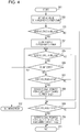
- a control flow performed when monitoring of a C1 voltage value is started will be described with reference to Fig. 4 .
- the flowchart illustrated in Fig. 4 is realized when the CPU 131 reads a program stored in the ROM 132 into the RAM 133 and executes the program.
- the waiting time corresponds to a period of time until the charge performed by the charge circuit 106 is completed, and is determined in advance in accordance with charge capability of the charge circuit 106 and capacity of the electrolytic capacitor 105.
- the CPU 131 sets an initial value (Toff) to an invalid period timer (S302). In this embodiment, 2 seconds is set as the initial value, for example.
- the CPU 131 reads a voltage level (a voltage value) of the electrolytic capacitor 105 through the input terminal PI1 and compares the voltage level with the threshold value voltage Vth_error so as to determine whether the voltage level is equal to or smaller than the threshold value voltage Vth_error (S303).
- the threshold value voltage Vth_error is predetermined for a determination as to whether the head power source voltage is close to the VM voltage. If the voltage of the electrolytic capacitor 105 (the C1 voltage) is close to the VM voltage, the voltage is larger than the threshold value voltage Vth_error.
- the threshold value voltage Vth_error is a threshold value for specifying failure of the power supply circuit and the head 3.
- the CPU 131 starts countdown of the invalid period timer (S304) since it is possible that instantaneous interruption or the like has occurred. It is determined whether the head voltage is equal to or smaller than the threshold value voltage Vth_error (S305).
- the CPU 131 determines whether a count value of the invalid period timer is zero (S306).
- the count value of the invalid period timer is zero (Yes in step S306), an error process is performed.
- the power supply to the head 3 through the power supply line is terminated.
- the FET 103 of Fig. 1 is turned off and the charge circuit 106 of Fig. 1 is turned off.
- the power source circuit 101 is turned off.
- the discharge circuit 107 may be turned on so that discharge is actively performed, for example.
- step S306 it is determined whether the head voltage is equal to or smaller than a threshold value Vth4 (S307).
- the process returns to step S305.
- the head power source control sequencer 122 outputs a signal from the output terminal PO2 so as to select the charge current value Ichg3 of the charge circuit 106 (S308). Specifically, the charge current value of the charge circuit 106 is switched from Ikeep to Ichg3. Thereafter the process returns to step S305.
- the head power source control sequencer 122 When the head voltage is not equal to or smaller than the threshold value Vth_error (No in step S305), it is determined whether the head voltage is equal to or larger than the threshold value Vth3 (S309). When it is determined that the head voltage is equal to or larger than the threshold value Vth3 (Yes in step S309), the head power source control sequencer 122 outputs a signal from the output terminal PO2 so as to select the charge current value Ikeep of the charge circuit 106 (S310) and the process is terminated (S311).
- the monitoring process is terminated.
- the charge current value Ichg3 is selected. Then, in the case where the count value is zero when it is determined that the head voltage is equal to or smaller than the threshold value Vth_error again, that is, the invalid period has elapsed, an error process is executed. In other words, in a case where the head voltage is equal to or smaller than the threshold value Vth_error even after the invalid period has elapsed (Yes in step S305 and step S306), an error process is executed.
- the capacitor voltage is monitored by periodically performing the operation described above.
- an error is not detected in the predetermined period of time (2 seconds, for example) set as the initial value (Toff) of the invalid period timer.
- the invalid period is set in accordance with a result of the determination as to whether the head voltage is equal to or smaller than the threshold value Vth_error, it is determined whether the head voltage is equal to or smaller than the threshold value Vth_error again after the set invalid period has elapsed, and it is determined whether an error process is to be performed in accordance with a result of the determination.
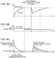
- the voltage of the electrolytic capacitor 105 and error detection at a time when instantaneous interruption occurs will be described with reference to Figs. 5A and 5B and Figs. 6A and 6B .
- FIGS. 5A and 5B are timing charts illustrating change of the voltage of the electrolytic capacitor 105 when voltage drop occurs owing to instantaneous interruption which occurs after the charge of the electrolytic capacitor 105 of the head 3 is completed and an error detection operation.
- the C1 voltage indicates the voltage of the electrolytic capacitor 105
- the VM voltage output from the power source circuit 101 is denoted by a dotted line.
- Ichg denotes a current value (a charge current value) of current to be supplied to the electrolytic capacitor 105
- Ikeep denotes a current value for detecting increase of leakage while the voltage of the electrolytic capacitor 105 is maintained. Accordingly, the current value Ikeep is smaller than the current value Ichg.
- the voltage (the C1 voltage) of the electrolytic capacitor 105 drops to the preset threshold value Vth_error owing to drop of the VM voltage output from the power source circuit 101.
- the instantaneous interruption means a case where applying of a voltage from the power source circuit 101 is temporarily stopped for a short time owing to external factors.
- An error detection invalid period (Toff) is set so that it is not determined that an error has occurred since failure occurs in the power supply circuit or a device at a time when the instantaneous interruption has occurred. If the voltage of the electrolytic capacitor 105 recovers within the set invalid period, inappropriate error detection is not performed. In a case where the C1 voltage is equal to or smaller than the threshold value Vth_error when the invalid period (Toff) has elapsed after the error operation is started, an error is detected and the electric power is blocked (current supply is stopped).
- a voltage drop time of the C1 voltage is determined in accordance with a leakage current ILeak and current supplied from the charge circuit 106.
- a leakage current ILeak and current supplied from the charge circuit 106.
- the C1 voltage gradually drops when leakage occurs, and therefore, a long period of time is required until the C1 voltage drops to the threshold value voltage Vth_error for start of the error detection process. Accordingly, a long period of time is required before the error detection operation is started.
- the CPU 131 sets the current value Ikeep which is sufficiently smaller than the current value Ichg after the charge is completed. Then, when the voltage of the electrolytic capacitor 105 becomes equal to or smaller than the threshold value Vth_error owing to the instantaneous interruption or the like and further equal to or smaller than the preset threshold value Vth4, the CPU 131 switches the maintaining current Ikeep to the charge current Ichg.
- a period of time from when the voltage drops owing to the instantaneous interruption to when the voltage recovers to the voltage at a time of the completion of the charge may be reduced. Furthermore, if the voltage of the electrolytic capacitor 105 recovers to a voltage which is sufficiently close to the VM voltage (here, the threshold value Vth3) or more, the CPU 131 switches the current value output from the charge circuit 106 to the maintaining current Ikeep again. By this, high accuracy of detection of leakage is attained. Furthermore, if current leakage occurs in a state in which the maintaining current Ikeep which is sufficiently smaller than the charge current Ichg is supplied, the voltage of the electrolytic capacitor 105 quickly drops. Therefore, the error detection operation is started immediately after the occurrence of leakage. Accordingly, a period of time from the occurrence of leakage to completion of the error process is reduced.
- the CPU 131 detects that the voltage (the C1 voltage) of the electrolytic capacitor 105 is equal to or smaller than the threshold value Vth4, the CPU 131 switches the maintaining current Ikeep to the charge current Ichg. However, the voltage does not rise while the leakage occurs. Therefore, an error is detected after the invalid period (Toff) has elapsed. After an error is detected, the electric power is blocked.
- Figs. 12A and 12B are diagrams illustrating management of states in the head power source control sequencer 122.
- a state in which the head 3 is turned off is denoted by a "standby 1001".
- a charge state 1002 is entered so that the head 3 is turned on.
- the C1 voltage becomes equal to or larger than the threshold value Vth3 and the charge is completed, a maintaining state 1003 of Fig. 12A is entered.
- the charge circuit 106 switches current to be supplied from Ichg to Ikeep.
- Fig. 12B is a diagram illustrating state transition in a case where the maintaining state 1003 is described in detail.
- a first charge state 1003_2 is entered as illustrated in Fig. 12B .
- the charge circuit 106 switches current to be supplied from Ikeep to Ichg.
- the C1 voltage exceeds the threshold value Vth3
- the first charge state 1003_2 is switched to the first maintaining state 1003_1.
- the charge circuit 106 switches current to be supplied from Ichg to Ikeep.
- a printing operation state 1004 is entered.
- the maintaining state 1003 and the printing operation state 1004 are alternately entered until the print job is completed.
- a discharge state 1005 is entered. Even in a case where failure is detected while the C1 voltage is monitored, the discharge state 1005 is entered. Although it is likely that failure is detected while the C1 voltage is monitored especially in the maintaining state 1003, if failure is detected in the printing operation state 1004, the discharge state 1005 may be immediately entered.
- the current value Ikeep will now be described.
- electric charge may be reduced owing to various reasons and discharge may be naturally performed even when failure does not occur in the device including the power supply circuit and the electric load.
- Examples of such natural discharge current include current supplied to the resistances 111 and 112 of Fig. 1 for detection and leakage current naturally generated since the head 3 is manufactured by a semiconductor process.
- the printing operation may be immediately started even when a certain period of time has elapsed after the charge operation. Accordingly, a value larger than these natural discharge currents is set to the current value Ikeep.
- the natural discharge current may be estimated in advance from the configuration of the power supply circuit and the configuration of the device including the load.
- the current value Ikeep is larger than the estimated natural discharge current.
- an upper limit of the current value Ikeep will be described with reference to Figs. 7A and 7B and Figs. 8A and 8B .
- a speed of drop of the voltage (the C1 voltage) of the electrolytic capacitor 105 at the time when the leakage other than the natural discharge occurs is determined by "ILeak-Ikeep".
- the maintaining current Ikeep is a large current value (a current value substantially equal to the charge current Ichg, for example), a long period of time is required before the voltage (the C1 voltage) of the electrolytic capacitor 105 becomes smaller than the error detection voltage (Vth_error), and accordingly, a long period of time is required for detection of failure.
- a value equal to or smaller than a specific value is set to the current value Ikeep so that failure may be detected at an appropriate timing in the leakage current ILeak in a failure state.
- the current value Ikeep may be set such that an amount of heat of VM ⁇ Ikeep is included in an allowable range.
- a period of time from when the capacitor voltage drops to when the error detection is started may be reduced by reducing the current value after the charge is completed to be smaller than the current value at the time of charging, and accordingly, occurrence of failure in the head power source circuit may be appropriately specified. Specifically, when current is abnormally leaked from the recording head 3, the leakage current may be immediately detected and power supply to the recording head 3 may be stopped.
- leakage current of the head 3 may be appropriately detected without deteriorating performance of the printer.
- failure may be reliably specified while a charge time of the electrolytic capacitor 105 is reduced when the failure occurs in the power supply circuit or the load.
- failure may be reliably specified while a charge time of the electrolytic capacitor 105 is reduced when the failure occurs in the power supply circuit or the load.
- the CPU 131 detects occurrence of rapid drop of a voltage even in the maintaining state after the charge of the electrolytic capacitor 105 is completed, and charge current is switched.
- charge current is switched in accordance with a voltage difference between a voltage (a VM voltage) of a power source circuit 101 and a voltage (a C1 voltage) of an electrolytic capacitor 105. Descriptions the same as those of the first embodiment are omitted. Reference numerals the same as those of the first embodiment are used for the same components.
- a CPU 131 sets a current value Ikeep as current supplied from a charge circuit 106. Thereafter, when instantaneous interruption occurs, although a voltage (a VM voltage) output from the power source circuit 101 immediately recovers, a long period of time is required for recovering the voltage (the C1 voltage) of the electrolytic capacitor 105 since charge current is restricted by the current value Ikeep.
- a FET 103 serving as a charge switch has thermal restriction and a setting is performed such that heat calculated by a product of a potential difference between a source and a drain and supplied current satisfies allowable power dissipation of the FET 103 of the charge circuit 106.
- the potential difference is VM-C1 and the current is Ion
- an amount of generated heat is represented by "(VM-C1) ⁇ Ion”.
- a period of time in which the apparatus is used over the thermal restriction in a case where large current is supplied while the potential difference between the voltage of the electrolytic capacitor 105 and the VM voltage is large, for example, is preferably shorter.
- the charge current is switched to a current value Ichg which is larger than the current value Ikeep.
- the voltage detection circuit 134 illustrated in Fig. 1 reads voltages divided by the resistances 113 and 114 as the VM voltage using an input terminal PI2 of the voltage detection circuit 134. Furthermore, the voltage detection circuit 134 reads voltages divided by the resistances 111 and 112 as the C1 voltage using an input terminal PI1 of the voltage detection circuit 134. When a difference between the read VM voltage and the read C1 voltage is equal to or larger than a predetermined threshold value for current switching, the charge current value is switched from Ikeep to Ichg.
- the threshold value for current switching is defined in accordance with a calculation formula obtained by the allowable power dissipation of the FET, and is smaller than a voltage of a Vds monitor, for example.
- the voltage monitoring is performed after the charge is completed and before the discharge is started, or in the first charge state and the first maintaining state in Fig. 12B .
- the voltage of the electrolytic capacitor 105 is monitored so that malfunction caused by drop of power source voltage owing to instantaneous interruption which occurs before start of operation of the recording head 3 or which occurs while the recording head 3 is stopped is prevented.
- a head power source control sequencer 122 performs control such that a current value is increased.
- a program for executing this process is periodically activated, for example, every 10 ms, using a timer incorporated in the CPU 131 in a period of time from when a predetermined period of time is elapsed after the process in step S202 is started to when discharge process of step S219 is started.
- a control flow performed when monitoring of the C1 voltage is started will be described with reference to Fig. 11 .
- the flowchart illustrated in Fig. 11 is realized when the CPU 131 reads a program stored in a ROM 132 into a RAM 133 and executes the program.
- the charge circuit 106 After the charge circuit 106 starts charge of the electrolytic capacitor 105 (S202) and a predetermined waiting time is elapsed, voltage monitoring is started (S1001).
- the waiting time corresponds to a period of time before the charge performed by the charge circuit 106 is completed, and is determined in advance in accordance with charge capability of the charge circuit 106 and capacity of the electrolytic capacitor 105.
- the CPU 131 sets an initial value (Toff) to an invalid period timer (S1002). In this embodiment, 2 seconds is set as the initial value, for example.
- the voltage detection circuit 134 illustrated in Fig. 1 reads voltages divided by the resistances 113 and 114 as the VM voltage using the input terminal PI2 of the voltage detection circuit 134. Furthermore, the voltage detection circuit 134 reads voltages divided by the resistances 111 and 112 as the C1 voltage using the input terminal PI1 of the voltage detection circuit 134. Then the CPU 131 determines whether a difference between the VM voltage and the read C1 voltage is equal to or larger than a predetermined threshold value (S1003).
- the predetermined threshold value is used to specify failure of the power supply circuit or the head 3. When the difference between the VM voltage and the C1 voltage is equal to or larger than the predetermined threshold value and a predetermined period of time has elapsed, it is determined that failure occurs in at least one of the power supply circuit and the head 3.
- step S1003 When the difference between the VM voltage and the C1 voltage is equal to or larger than the predetermined threshold value (Yes in step S1003), the CPU 131 starts countdown using the invalid period timer since it is possible that instantaneous interruption has occurred (S1004). Then the CPU 131 determines whether a difference between the VM voltage and the C1 voltage is equal to or larger than the predetermined threshold value (S1005).
- the CPU 131 determines whether a count value of the invalid period timer is zero (S1006). When the count value of the invalid period timer is zero (Yes in step S1006), an error process is performed.
- the head power source control sequencer 122 outputs a signal from an output terminal PO2 so as to select a charge current value Ichg3 of the charge circuit 106 (S1007). Specifically, the charge current value of the charge circuit 106 is switched from Ikeep to Ichg3. Thereafter the process returns to step S1005.
- step S1005 When the difference between the VM voltage and the C1 voltage is not equal to or larger than the predetermined threshold value (No in step S1005), it is determined whether the head voltage is equal to or larger than a threshold value Vth3 (S1008). When it is determined that the head voltage is equal to or larger than the threshold value Vth3 (Yes in step S1008), the head power source control sequencer 122 outputs a signal from the output terminal PO2 so as to select a charge current value Ikeep of the charge circuit 106 (S1009) and the process is terminated (S1010).
- the capacitor voltage is monitored by periodically performing the operation described above.
- an error is not detected in a predetermined period of time (2 seconds, for example) set as the initial value (Toff) of the invalid period timer.
- This embodiment may obtain the effects of the first embodiment.
- the present invention is not limited to the foregoing embodiments.
- the power supply apparatus includes the head as the electric load in the foregoing embodiments, the present invention is not limited to this, and the power supply apparatus may not include the electric load.
- the power supply apparatus may be connectable to the electric load and may supply electric power to the electric load.
- a current value supplied from the charge circuit 106 is switched when the electrolytic capacitor 105 is charged in the foregoing embodiments, the present invention is not limited to this, and a current value supplied from the charge circuit 106 may be constant.
Landscapes
- Engineering & Computer Science (AREA)
- Power Engineering (AREA)
- Ink Jet (AREA)
- Accessory Devices And Overall Control Thereof (AREA)
- Charge And Discharge Circuits For Batteries Or The Like (AREA)
- Particle Formation And Scattering Control In Inkjet Printers (AREA)
Claims (16)
- Energieversorgungsvorrichtung zum Versorgen eines elektrischen Verbrauchers (3) mit Energie über eine Energieversorgungsleitung, wobei die Energieversorgungsvorrichtung umfasst:eine Energiequelleneinrichtung (101), die konfiguriert ist, über die Energieversorgungsleitung elektrische Energie bereitzustellen;einen Kondensator (105), der mit der Energieversorgungsleitung verbunden ist;eine Ladeschaltung (106), die konfiguriert ist, von der Energiequelleneinrichtung (101) Energie zu empfangen und einen Stromwert zum Laden des Kondensators auszugeben;eine Detektionseinrichtung (134), die konfiguriert ist, einen Spannungswert des Kondensators (105) zu detektieren;eine Steuereinrichtung (122), die konfiguriert ist, nach abgeschlossener Ladung des Kondensators von einem vor abgeschlossener Ladung des Kondensators bereitgestellten ersten Stromwert auf einen zweiten Stromwert umzuschalten, der niedriger ist als der erste Stromwert, dadurch gekennzeichnet, dass die Vorrichtung ferner umfasst:eine erste Bestimmungseinrichtung (122), die konfiguriert ist, basierend auf dem nach abgeschlossener Ladung des Kondensators durch die Detektionseinrichtung detektierten Spannungswert zu bestimmen, ob eine erste Bedingung erfüllt ist; undeine zweite Bestimmungseinrichtung (122), die konfiguriert ist zum Bestimmen, ob eine Fehlerverarbeitung innerhalb eines vorbestimmten Zeitraums, nachdem die erste Bestimmungseinrichtung bestimmt, dass die erste Bedingung erfüllt ist, durchgeführt werden soll, falls die erste Bedingung erfüllt ist,wobei die Steuereinrichtung (122) ferner konfiguriert ist, die Ladeschaltung (106) so zu steuern, dass diese von dem von der Ladeschaltung ausgegebenen zweiten Stromwert auf einen dritten Stromwert umschaltet, welcher höher ist als der zweite Stromwert, falls die erste Bestimmungseinrichtung nach vollständiger Ladung des Kondensators bestimmt, dass die erste Bedingung erfüllt ist.
- Energieversorgungsvorrichtung nach Anspruch 1, wobei die erste Bestimmungseinrichtung bestimmt, dass die erste Bedingung erfüllt ist, falls der durch die Detektionseinrichtung detektierte Spannungswert gleich hoch wie oder niedriger als ein vorbestimmter Schwellenwert ist.
- Energieversorgungsvorrichtung nach Anspruch 1 oder 2,wobeidie erste Bestimmungseinrichtung konfiguriert ist, zu bestimmen, dass die erste Bedingung erfüllt ist, falls der durch die Detektionseinrichtung detektierte Spannungswert gleich hoch wie oder niedriger als ein erster Schwellenwert ist,die erste Bestimmungseinrichtung ferner konfiguriert ist, zu bestimmen, ob der durch die Detektionseinrichtung detektierte Spannungswert gleich hoch wie oder niedriger als ein zweiter Schwellenwert ist, welcher niedriger ist als der erste Schwellenwert, falls bestimmt wird, dass die erste Bedingung nach vollständiger Ladung des Kondensators erfüllt ist,die Steuereinrichtung ferner konfiguriert ist, den von der Ladeschaltung ausgegebenen Stromwert auf den dritten Stromwert, der höher ist als der zweite Stromwert, umzuschalten, falls die erste Bestimmungseinrichtung bestimmt, dass der durch die Detektionseinrichtung detektierte Stromwert gleich hoch wie oder niedriger als der zweite Schwellenwert ist, unddie erste Bestimmungseinrichtung ferner konfiguriert ist, zu bestimmen, ob die erste Bedingung erfüllt ist, falls der vorbestimmte Zeitraum abgelaufen ist, nachdem bestimmt wurde, dass die erste Bedingung erfüllt ist.
- Energieversorgungsvorrichtung nach einem der Ansprüche 1 bis 3, ferner umfassend:eine zweite Detektionseinrichtung (134), die konfiguriert ist, einen Spannungswert der Stromquelleneinrichtung zu detektieren,wobei die erste Bestimmungseinrichtung bestimmt, dass die erste Bedingung erfüllt ist, falls ein Unterschied zwischen dem durch die Detektionseinrichtung nach vollständiger Ladung des Kondensators detektierten Spannungswert und dem durch die zweite Detektionseinrichtung detektierten Spannungswert gleich groß wie oder größer als ein vorbestimmter Schwellenwert ist.
- Energieversorgungsvorrichtung nach einem der Ansprüche 1 bis 4, wobei eine durch die Energieversorgungsleitung bereitgestellte Energieversorgung des elektrischen Verbrauchers abgebrochen wird, falls die zweite Bestimmungseinrichtung bestimmt, dass die Fehlerverarbeitung durchgeführt werden soll.
- Energieversorgungsvorrichtung nach Anspruch 5, wobei die Energiequelleneinrichtung (101) deaktiviert wird, falls die zweite Bestimmungseinrichtung (122) bestimmt, dass die Fehlerverarbeitung durchgeführt werden soll.
- Energieversorgungsvorrichtung nach einem der Ansprüche 1 bis 6, wobei der dritte Stromwert dem ersten Stromwert entspricht.
- Energieversorgungsvorrichtung nach einem der Ansprüche 1 bis 7, wobei der elektrische Verbraucher (3) ein Druckkopf ist.
- Energieversorgungsvorrichtung nach einem der Ansprüche 1 bis 8, die ferner den elektrischen Verbraucher (3) umfasst.
- Steuerverfahren zum Steuern einer Energieversorgungsvorrichtung zum Versorgen eines elektrischen Verbrauchers (3) mit Energie über eine Energieversorgungsleitung, wobei die Energieversorgungsvorrichtung umfasst:eine Energiequelleneinrichtung (101), die konfiguriert ist, über die Energieversorgungsleitung elektrische Energie bereitzustellen;einen Kondensator (105), der mit der Energieversorgungsleitung verbunden ist;eine Ladeschaltung (106), die konfiguriert ist, von der Energiequelleneinrichtung (101) Energie zu empfangen und einen Stromwert zum Laden des Kondensators auszugeben;wobei das Steuerverfahren umfasst:Umschalten von einem vor abgeschlossener Ladung des Kondensators bereitgestellten ersten Stromwert auf einen zweiten Stromwert, der niedriger ist als der der erste Stromwert, nach abgeschlossener Ladung des Kondensators;Detektieren eines Spannungswerts des Kondensators; undBestimmen, ob eine erste Bedingung erfüllt ist, basierend auf dem nach abgeschlossener Ladung des Kondensators detektierten Spannungswert,Bestimmen ob innerhalb eines vorbestimmten Zeitraums nach Bestimmen, dass die erste Bedingung erfüllt ist, eine Fehlerverarbeitung durchgeführt werden soll,dadurch gekennzeichnet, dassfalls bestimmt wird, dass die erste Bedingung nach vollständiger Ladung des Kondensators erfüllt ist, der von der Ladeschaltung bereitgestellte zweite Stromwert auf einen dritten Stromwert umgeschaltet wird, der höher ist als der zweite Stromwert.
- Steuerverfahren nach Anspruch 10, wobei bestimmt wird, dass die erste Bedingung erfüllt ist, falls der detektierte Spannungswert des Kondensators gleich hoch wie oder niedriger als ein vorbestimmter Schwellenwert ist.
- Steuerverfahren nach Anspruch 10 oder 11, wobei auf den dritten Stromwert, welcher größer ist als der zweite Stromwert, umgeschaltet wird, falls bestimmt wird, dass der detektierte Spannungswert des Kondensators gleich hoch wie oder niedriger als ein erster Schwellenwert ist, und außerdem bestimmt wird, dass der detektierte Spannungswert des Kondensators nach abgeschlossener Ladung des Kondensators gleich hoch wie oder niedriger als ein zweiter Schwellenwert ist, welcher niedriger ist als der erste Schwellenwert.
- Steuerverfahren nach einem der Ansprüche 10 bis 12, ferner umfassend:Detektieren eines Spannungswerts der Stromquelleneinrichtung, undBestimmen, dass die erste Bedingung erfüllt ist, falls ein Unterschied zwischen dem detektierten Spannungswert des Kondensators und dem detektierten Spannungswert der Energiequelleneinrichtung nach vollständiger Ladung des Kondensators gleich groß wie oder größer als ein vorbestimmter Schwellenwert ist.
- Steuerverfahren nach einem der Ansprüche 10 bis 13, wobei der dritte Stromwert dem ersten Stromwert entspricht.
- Computerprogramm, umfassend Anweisungen, die bei Ausführen des Programms durch einen Computer den Computer veranlassen, das Verfahren nach einem der Ansprüche 10 bis 14 auszuführen.
- Computerlesbares Medium, umfassend Anweisungen, die bei Ausführen durch einen Computer den Computer veranlassen, das Verfahren nach einem der Ansprüche 10 bis 14 auszuführen.
Applications Claiming Priority (1)
| Application Number | Priority Date | Filing Date | Title |
|---|---|---|---|
| JP2015107869A JP6452548B2 (ja) | 2015-05-27 | 2015-05-27 | 電力供給装置及び制御方法 |
Publications (2)
| Publication Number | Publication Date |
|---|---|
| EP3113318A1 EP3113318A1 (de) | 2017-01-04 |
| EP3113318B1 true EP3113318B1 (de) | 2018-07-18 |
Family
ID=56081333
Family Applications (1)
| Application Number | Title | Priority Date | Filing Date |
|---|---|---|---|
| EP16171478.7A Active EP3113318B1 (de) | 2015-05-27 | 2016-05-26 | Stromversorgungsvorrichtung und steuerungsverfahren |
Country Status (4)
| Country | Link |
|---|---|
| US (1) | US9862216B2 (de) |
| EP (1) | EP3113318B1 (de) |
| JP (1) | JP6452548B2 (de) |
| CN (1) | CN106183480B (de) |
Families Citing this family (7)
| Publication number | Priority date | Publication date | Assignee | Title |
|---|---|---|---|---|
| JP6419025B2 (ja) * | 2015-05-27 | 2018-11-07 | キヤノン株式会社 | 電力供給装置、プリンタ及び制御方法 |
| US10381166B2 (en) * | 2016-05-25 | 2019-08-13 | Vishay Sprague, Inc. | High performance and reliability solid electrolytic tantalum capacitors and screening method |
| JP6972684B2 (ja) * | 2017-06-15 | 2021-11-24 | コニカミノルタ株式会社 | 記録装置及び記録ヘッド電圧設定方法 |
| CN107703787B (zh) * | 2017-08-17 | 2018-11-16 | 北京通州皇家印刷厂 | 基于大数据的数码印刷装置故障控制方法 |
| US10634713B2 (en) * | 2018-02-22 | 2020-04-28 | Piecemakers Technology, Inc. | Method for testing semiconductor die pad untouched by probe and related test circuit |
| JP7392548B2 (ja) * | 2020-03-30 | 2023-12-06 | ブラザー工業株式会社 | 印刷装置 |
| JP7508975B2 (ja) * | 2020-09-28 | 2024-07-02 | オムロン株式会社 | モバイルロボット、モバイルマニピュレータ、およびモバイルロボットの制御方法 |
Family Cites Families (14)
| Publication number | Priority date | Publication date | Assignee | Title |
|---|---|---|---|---|
| EP1136907B1 (de) * | 1993-12-09 | 2006-04-26 | Canon Kabushiki Kaisha | Datenverarbeitungsgerät das als Host arbeitet und Verfahren um das Datenverarbeitungsgerät zu steuern |
| JPH08180907A (ja) | 1994-12-26 | 1996-07-12 | Sony Corp | 充電器 |
| US6975098B2 (en) * | 2002-01-31 | 2005-12-13 | Vlt, Inc. | Factorized power architecture with point of load sine amplitude converters |
| US6977492B2 (en) * | 2002-07-10 | 2005-12-20 | Marvell World Trade Ltd. | Output regulator |
| US6825675B1 (en) * | 2003-06-27 | 2004-11-30 | Lexmark International, Inc. | Method for detecting a shorted printhead in a printer having at least two printheads |
| JP4095004B2 (ja) * | 2003-09-12 | 2008-06-04 | 株式会社リコー | 電源装置および画像形成装置 |
| JP2007259632A (ja) * | 2006-03-24 | 2007-10-04 | Nec Personal Products Co Ltd | 充電回路及び充電制御方法 |
| US7449862B1 (en) | 2006-09-29 | 2008-11-11 | Motorola, Inc. | Method and apparatus for charging a battery using a threshold to cease charging |
| JP5094564B2 (ja) * | 2008-06-02 | 2012-12-12 | キヤノン株式会社 | 記録装置 |
| US8212536B2 (en) * | 2009-12-23 | 2012-07-03 | R2 Semiconductor, Inc. | Stacked NMOS DC-to-DC power conversion |
| JP2012120267A (ja) * | 2010-11-29 | 2012-06-21 | Toshiba Corp | 充電制御装置 |
| CN104335447B (zh) * | 2012-04-02 | 2017-07-18 | 施耐德电气It公司 | 电源控制 |
| JP2014000743A (ja) * | 2012-06-19 | 2014-01-09 | Canon Inc | 記録装置 |
| US9048679B2 (en) | 2012-06-28 | 2015-06-02 | Blackberry Limited | Maximized battery capacity charge based on equilibrium charging |
-
2015
- 2015-05-27 JP JP2015107869A patent/JP6452548B2/ja active Active
-
2016
- 2016-05-24 US US15/163,439 patent/US9862216B2/en active Active
- 2016-05-26 EP EP16171478.7A patent/EP3113318B1/de active Active
- 2016-05-26 CN CN201610361808.1A patent/CN106183480B/zh active Active
Non-Patent Citations (1)
| Title |
|---|
| None * |
Also Published As
| Publication number | Publication date |
|---|---|
| CN106183480B (zh) | 2019-01-11 |
| JP2016221715A (ja) | 2016-12-28 |
| US20160347103A1 (en) | 2016-12-01 |
| EP3113318A1 (de) | 2017-01-04 |
| JP6452548B2 (ja) | 2019-01-16 |
| CN106183480A (zh) | 2016-12-07 |
| US9862216B2 (en) | 2018-01-09 |
Similar Documents
| Publication | Publication Date | Title |
|---|---|---|
| EP3113318A1 (de) | Stromversorgungsvorrichtung und steuerungsverfahren | |
| KR101107778B1 (ko) | 전지 회로의 제어 장치, 충전 제어 장치, 이것을 사용한 전자기기, 및 제어 방법 | |
| US7675196B2 (en) | Power supply apparatus and image forming apparatus | |
| US8761631B2 (en) | Power supply including zero-cross detection circuit, and image forming apparatus | |
| EP3112157B1 (de) | Stromversorgungsvorrichtung, drucker und steuerungsverfahren | |
| US20130147875A1 (en) | Recording apparatus | |
| KR970003190B1 (ko) | 충전제어장치 및 이러한 충전제어장치를 구비한 전자기기 | |
| JP2012125928A (ja) | 記録装置、および、電源装置 | |
| JP2010093912A (ja) | 電源装置 | |
| EP3098074A1 (de) | Steuerungsvorrichtung und steuerungsverfahren dafür | |
| JP6576103B2 (ja) | 電力供給装置、プリンタ及び制御方法 | |
| JP2017118696A (ja) | 充電装置、プリンター、及び、充電方法 | |
| JP6501616B2 (ja) | 電力供給装置、プリンタ及び制御方法 | |
| JP3428981B2 (ja) | 電子機器 | |
| JPH07322528A (ja) | 電子機器及びその制御方法 | |
| JP2001157375A (ja) | 電池の充電制御装置及び充電制御方法 | |
| JP2023129917A (ja) | 電源制御ic、及び電源制御システム | |
| JP2006325319A (ja) | ブラシレスモータ駆動装置及び画像形成装置 | |
| JP2025086728A (ja) | 記録装置、制御方法、およびプログラム | |
| JP2024073788A (ja) | 印刷装置 | |
| JP2022090312A (ja) | 印刷装置 | |
| JP2007047472A (ja) | 画像形成装置 | |
| JP2017114008A (ja) | 電源装置、画像形成装置及びその制御方法 | |
| JP2004220915A (ja) | 加熱装置、定着装置及び画像形成装置 |
Legal Events
| Date | Code | Title | Description |
|---|---|---|---|
| PUAI | Public reference made under article 153(3) epc to a published international application that has entered the european phase |
Free format text: ORIGINAL CODE: 0009012 |
|
| STAA | Information on the status of an ep patent application or granted ep patent |
Free format text: STATUS: THE APPLICATION HAS BEEN PUBLISHED |
|
| AK | Designated contracting states |
Kind code of ref document: A1 Designated state(s): AL AT BE BG CH CY CZ DE DK EE ES FI FR GB GR HR HU IE IS IT LI LT LU LV MC MK MT NL NO PL PT RO RS SE SI SK SM TR |
|
| AX | Request for extension of the european patent |
Extension state: BA ME |
|
| STAA | Information on the status of an ep patent application or granted ep patent |
Free format text: STATUS: REQUEST FOR EXAMINATION WAS MADE |
|
| 17P | Request for examination filed |
Effective date: 20170704 |
|
| RBV | Designated contracting states (corrected) |
Designated state(s): AL AT BE BG CH CY CZ DE DK EE ES FI FR GB GR HR HU IE IS IT LI LT LU LV MC MK MT NL NO PL PT RO RS SE SI SK SM TR |
|
| STAA | Information on the status of an ep patent application or granted ep patent |
Free format text: STATUS: EXAMINATION IS IN PROGRESS |
|
| 17Q | First examination report despatched |
Effective date: 20170824 |
|
| GRAP | Despatch of communication of intention to grant a patent |
Free format text: ORIGINAL CODE: EPIDOSNIGR1 |
|
| STAA | Information on the status of an ep patent application or granted ep patent |
Free format text: STATUS: GRANT OF PATENT IS INTENDED |
|
| INTG | Intention to grant announced |
Effective date: 20180109 |
|
| GRAS | Grant fee paid |
Free format text: ORIGINAL CODE: EPIDOSNIGR3 |
|
| GRAA | (expected) grant |
Free format text: ORIGINAL CODE: 0009210 |
|
| STAA | Information on the status of an ep patent application or granted ep patent |
Free format text: STATUS: THE PATENT HAS BEEN GRANTED |
|
| AK | Designated contracting states |
Kind code of ref document: B1 Designated state(s): AL AT BE BG CH CY CZ DE DK EE ES FI FR GB GR HR HU IE IS IT LI LT LU LV MC MK MT NL NO PL PT RO RS SE SI SK SM TR |
|
| REG | Reference to a national code |
Ref country code: GB Ref legal event code: FG4D |
|
| REG | Reference to a national code |
Ref country code: CH Ref legal event code: EP |
|
| REG | Reference to a national code |
Ref country code: IE Ref legal event code: FG4D |
|
| REG | Reference to a national code |
Ref country code: AT Ref legal event code: REF Ref document number: 1020398 Country of ref document: AT Kind code of ref document: T Effective date: 20180815 |
|
| REG | Reference to a national code |
Ref country code: DE Ref legal event code: R096 Ref document number: 602016004080 Country of ref document: DE |
|
| REG | Reference to a national code |
Ref country code: NL Ref legal event code: MP Effective date: 20180718 |
|
| REG | Reference to a national code |
Ref country code: LT Ref legal event code: MG4D |
|
| REG | Reference to a national code |
Ref country code: AT Ref legal event code: MK05 Ref document number: 1020398 Country of ref document: AT Kind code of ref document: T Effective date: 20180718 |
|
| PG25 | Lapsed in a contracting state [announced via postgrant information from national office to epo] |
Ref country code: NL Free format text: LAPSE BECAUSE OF FAILURE TO SUBMIT A TRANSLATION OF THE DESCRIPTION OR TO PAY THE FEE WITHIN THE PRESCRIBED TIME-LIMIT Effective date: 20180718 |
|
| PG25 | Lapsed in a contracting state [announced via postgrant information from national office to epo] |
Ref country code: GR Free format text: LAPSE BECAUSE OF FAILURE TO SUBMIT A TRANSLATION OF THE DESCRIPTION OR TO PAY THE FEE WITHIN THE PRESCRIBED TIME-LIMIT Effective date: 20181019 Ref country code: SE Free format text: LAPSE BECAUSE OF FAILURE TO SUBMIT A TRANSLATION OF THE DESCRIPTION OR TO PAY THE FEE WITHIN THE PRESCRIBED TIME-LIMIT Effective date: 20180718 Ref country code: NO Free format text: LAPSE BECAUSE OF FAILURE TO SUBMIT A TRANSLATION OF THE DESCRIPTION OR TO PAY THE FEE WITHIN THE PRESCRIBED TIME-LIMIT Effective date: 20181018 Ref country code: BG Free format text: LAPSE BECAUSE OF FAILURE TO SUBMIT A TRANSLATION OF THE DESCRIPTION OR TO PAY THE FEE WITHIN THE PRESCRIBED TIME-LIMIT Effective date: 20181018 Ref country code: RS Free format text: LAPSE BECAUSE OF FAILURE TO SUBMIT A TRANSLATION OF THE DESCRIPTION OR TO PAY THE FEE WITHIN THE PRESCRIBED TIME-LIMIT Effective date: 20180718 Ref country code: LT Free format text: LAPSE BECAUSE OF FAILURE TO SUBMIT A TRANSLATION OF THE DESCRIPTION OR TO PAY THE FEE WITHIN THE PRESCRIBED TIME-LIMIT Effective date: 20180718 Ref country code: PL Free format text: LAPSE BECAUSE OF FAILURE TO SUBMIT A TRANSLATION OF THE DESCRIPTION OR TO PAY THE FEE WITHIN THE PRESCRIBED TIME-LIMIT Effective date: 20180718 Ref country code: FI Free format text: LAPSE BECAUSE OF FAILURE TO SUBMIT A TRANSLATION OF THE DESCRIPTION OR TO PAY THE FEE WITHIN THE PRESCRIBED TIME-LIMIT Effective date: 20180718 Ref country code: IS Free format text: LAPSE BECAUSE OF FAILURE TO SUBMIT A TRANSLATION OF THE DESCRIPTION OR TO PAY THE FEE WITHIN THE PRESCRIBED TIME-LIMIT Effective date: 20181118 Ref country code: AT Free format text: LAPSE BECAUSE OF FAILURE TO SUBMIT A TRANSLATION OF THE DESCRIPTION OR TO PAY THE FEE WITHIN THE PRESCRIBED TIME-LIMIT Effective date: 20180718 |
|
| PG25 | Lapsed in a contracting state [announced via postgrant information from national office to epo] |
Ref country code: AL Free format text: LAPSE BECAUSE OF FAILURE TO SUBMIT A TRANSLATION OF THE DESCRIPTION OR TO PAY THE FEE WITHIN THE PRESCRIBED TIME-LIMIT Effective date: 20180718 Ref country code: LV Free format text: LAPSE BECAUSE OF FAILURE TO SUBMIT A TRANSLATION OF THE DESCRIPTION OR TO PAY THE FEE WITHIN THE PRESCRIBED TIME-LIMIT Effective date: 20180718 Ref country code: HR Free format text: LAPSE BECAUSE OF FAILURE TO SUBMIT A TRANSLATION OF THE DESCRIPTION OR TO PAY THE FEE WITHIN THE PRESCRIBED TIME-LIMIT Effective date: 20180718 |
|
| REG | Reference to a national code |
Ref country code: DE Ref legal event code: R097 Ref document number: 602016004080 Country of ref document: DE |
|
| PG25 | Lapsed in a contracting state [announced via postgrant information from national office to epo] |
Ref country code: IT Free format text: LAPSE BECAUSE OF FAILURE TO SUBMIT A TRANSLATION OF THE DESCRIPTION OR TO PAY THE FEE WITHIN THE PRESCRIBED TIME-LIMIT Effective date: 20180718 Ref country code: EE Free format text: LAPSE BECAUSE OF FAILURE TO SUBMIT A TRANSLATION OF THE DESCRIPTION OR TO PAY THE FEE WITHIN THE PRESCRIBED TIME-LIMIT Effective date: 20180718 Ref country code: CZ Free format text: LAPSE BECAUSE OF FAILURE TO SUBMIT A TRANSLATION OF THE DESCRIPTION OR TO PAY THE FEE WITHIN THE PRESCRIBED TIME-LIMIT Effective date: 20180718 Ref country code: RO Free format text: LAPSE BECAUSE OF FAILURE TO SUBMIT A TRANSLATION OF THE DESCRIPTION OR TO PAY THE FEE WITHIN THE PRESCRIBED TIME-LIMIT Effective date: 20180718 Ref country code: ES Free format text: LAPSE BECAUSE OF FAILURE TO SUBMIT A TRANSLATION OF THE DESCRIPTION OR TO PAY THE FEE WITHIN THE PRESCRIBED TIME-LIMIT Effective date: 20180718 |
|
| PLBE | No opposition filed within time limit |
Free format text: ORIGINAL CODE: 0009261 |
|
| STAA | Information on the status of an ep patent application or granted ep patent |
Free format text: STATUS: NO OPPOSITION FILED WITHIN TIME LIMIT |
|
| PG25 | Lapsed in a contracting state [announced via postgrant information from national office to epo] |
Ref country code: SK Free format text: LAPSE BECAUSE OF FAILURE TO SUBMIT A TRANSLATION OF THE DESCRIPTION OR TO PAY THE FEE WITHIN THE PRESCRIBED TIME-LIMIT Effective date: 20180718 Ref country code: DK Free format text: LAPSE BECAUSE OF FAILURE TO SUBMIT A TRANSLATION OF THE DESCRIPTION OR TO PAY THE FEE WITHIN THE PRESCRIBED TIME-LIMIT Effective date: 20180718 Ref country code: SM Free format text: LAPSE BECAUSE OF FAILURE TO SUBMIT A TRANSLATION OF THE DESCRIPTION OR TO PAY THE FEE WITHIN THE PRESCRIBED TIME-LIMIT Effective date: 20180718 |
|
| 26N | No opposition filed |
Effective date: 20190423 |
|
| PG25 | Lapsed in a contracting state [announced via postgrant information from national office to epo] |
Ref country code: SI Free format text: LAPSE BECAUSE OF FAILURE TO SUBMIT A TRANSLATION OF THE DESCRIPTION OR TO PAY THE FEE WITHIN THE PRESCRIBED TIME-LIMIT Effective date: 20180718 |
|
| REG | Reference to a national code |
Ref country code: CH Ref legal event code: PL |
|
| PG25 | Lapsed in a contracting state [announced via postgrant information from national office to epo] |
Ref country code: CH Free format text: LAPSE BECAUSE OF NON-PAYMENT OF DUE FEES Effective date: 20190531 Ref country code: LI Free format text: LAPSE BECAUSE OF NON-PAYMENT OF DUE FEES Effective date: 20190531 Ref country code: MC Free format text: LAPSE BECAUSE OF FAILURE TO SUBMIT A TRANSLATION OF THE DESCRIPTION OR TO PAY THE FEE WITHIN THE PRESCRIBED TIME-LIMIT Effective date: 20180718 |
|
| REG | Reference to a national code |
Ref country code: BE Ref legal event code: MM Effective date: 20190531 |
|
| PG25 | Lapsed in a contracting state [announced via postgrant information from national office to epo] |
Ref country code: LU Free format text: LAPSE BECAUSE OF NON-PAYMENT OF DUE FEES Effective date: 20190526 |
|
| PG25 | Lapsed in a contracting state [announced via postgrant information from national office to epo] |
Ref country code: TR Free format text: LAPSE BECAUSE OF FAILURE TO SUBMIT A TRANSLATION OF THE DESCRIPTION OR TO PAY THE FEE WITHIN THE PRESCRIBED TIME-LIMIT Effective date: 20180718 |
|
| PG25 | Lapsed in a contracting state [announced via postgrant information from national office to epo] |
Ref country code: IE Free format text: LAPSE BECAUSE OF NON-PAYMENT OF DUE FEES Effective date: 20190526 |
|
| PG25 | Lapsed in a contracting state [announced via postgrant information from national office to epo] |
Ref country code: BE Free format text: LAPSE BECAUSE OF NON-PAYMENT OF DUE FEES Effective date: 20190531 |
|
| PG25 | Lapsed in a contracting state [announced via postgrant information from national office to epo] |
Ref country code: PT Free format text: LAPSE BECAUSE OF FAILURE TO SUBMIT A TRANSLATION OF THE DESCRIPTION OR TO PAY THE FEE WITHIN THE PRESCRIBED TIME-LIMIT Effective date: 20181118 Ref country code: FR Free format text: LAPSE BECAUSE OF NON-PAYMENT OF DUE FEES Effective date: 20190531 |
|
| GBPC | Gb: european patent ceased through non-payment of renewal fee |
Effective date: 20200526 |
|
| PG25 | Lapsed in a contracting state [announced via postgrant information from national office to epo] |
Ref country code: GB Free format text: LAPSE BECAUSE OF NON-PAYMENT OF DUE FEES Effective date: 20200526 |
|
| PG25 | Lapsed in a contracting state [announced via postgrant information from national office to epo] |
Ref country code: CY Free format text: LAPSE BECAUSE OF FAILURE TO SUBMIT A TRANSLATION OF THE DESCRIPTION OR TO PAY THE FEE WITHIN THE PRESCRIBED TIME-LIMIT Effective date: 20180718 |
|
| PG25 | Lapsed in a contracting state [announced via postgrant information from national office to epo] |
Ref country code: HU Free format text: LAPSE BECAUSE OF FAILURE TO SUBMIT A TRANSLATION OF THE DESCRIPTION OR TO PAY THE FEE WITHIN THE PRESCRIBED TIME-LIMIT; INVALID AB INITIO Effective date: 20160526 Ref country code: MT Free format text: LAPSE BECAUSE OF FAILURE TO SUBMIT A TRANSLATION OF THE DESCRIPTION OR TO PAY THE FEE WITHIN THE PRESCRIBED TIME-LIMIT Effective date: 20180718 |
|
| PG25 | Lapsed in a contracting state [announced via postgrant information from national office to epo] |
Ref country code: MK Free format text: LAPSE BECAUSE OF FAILURE TO SUBMIT A TRANSLATION OF THE DESCRIPTION OR TO PAY THE FEE WITHIN THE PRESCRIBED TIME-LIMIT Effective date: 20180718 |
|
| PGFP | Annual fee paid to national office [announced via postgrant information from national office to epo] |
Ref country code: DE Payment date: 20250423 Year of fee payment: 10 |