EP3108286B1 - Anzeigevorrichtung - Google Patents
Anzeigevorrichtung Download PDFInfo
- Publication number
- EP3108286B1 EP3108286B1 EP15705502.1A EP15705502A EP3108286B1 EP 3108286 B1 EP3108286 B1 EP 3108286B1 EP 15705502 A EP15705502 A EP 15705502A EP 3108286 B1 EP3108286 B1 EP 3108286B1
- Authority
- EP
- European Patent Office
- Prior art keywords
- luminous
- display device
- light
- area
- areas
- Prior art date
- Legal status (The legal status is an assumption and is not a legal conclusion. Google has not performed a legal analysis and makes no representation as to the accuracy of the status listed.)
- Active
Links
Images


Classifications
-
- G—PHYSICS
- G02—OPTICS
- G02B—OPTICAL ELEMENTS, SYSTEMS OR APPARATUS
- G02B26/00—Optical devices or arrangements for the control of light using movable or deformable optical elements
- G02B26/02—Optical devices or arrangements for the control of light using movable or deformable optical elements for controlling the intensity of light
-
- G—PHYSICS
- G02—OPTICS
- G02B—OPTICAL ELEMENTS, SYSTEMS OR APPARATUS
- G02B6/00—Light guides; Structural details of arrangements comprising light guides and other optical elements, e.g. couplings
- G02B6/0001—Light guides; Structural details of arrangements comprising light guides and other optical elements, e.g. couplings specially adapted for lighting devices or systems
- G02B6/0005—Light guides; Structural details of arrangements comprising light guides and other optical elements, e.g. couplings specially adapted for lighting devices or systems the light guides being of the fibre type
- G02B6/0006—Coupling light into the fibre
-
- G—PHYSICS
- G02—OPTICS
- G02F—OPTICAL DEVICES OR ARRANGEMENTS FOR THE CONTROL OF LIGHT BY MODIFICATION OF THE OPTICAL PROPERTIES OF THE MEDIA OF THE ELEMENTS INVOLVED THEREIN; NON-LINEAR OPTICS; FREQUENCY-CHANGING OF LIGHT; OPTICAL LOGIC ELEMENTS; OPTICAL ANALOGUE/DIGITAL CONVERTERS
- G02F1/00—Devices or arrangements for the control of the intensity, colour, phase, polarisation or direction of light arriving from an independent light source, e.g. switching, gating or modulating; Non-linear optics
- G02F1/01—Devices or arrangements for the control of the intensity, colour, phase, polarisation or direction of light arriving from an independent light source, e.g. switching, gating or modulating; Non-linear optics for the control of the intensity, phase, polarisation or colour
- G02F1/13—Devices or arrangements for the control of the intensity, colour, phase, polarisation or direction of light arriving from an independent light source, e.g. switching, gating or modulating; Non-linear optics for the control of the intensity, phase, polarisation or colour based on liquid crystals, e.g. single liquid crystal display cells
- G02F1/133—Constructional arrangements; Operation of liquid crystal cells; Circuit arrangements
- G02F1/1333—Constructional arrangements; Manufacturing methods
- G02F1/1335—Structural association of cells with optical devices, e.g. polarisers or reflectors
- G02F1/1336—Illuminating devices
- G02F1/133602—Direct backlight
- G02F1/133603—Direct backlight with LEDs
-
- H—ELECTRICITY
- H10—SEMICONDUCTOR DEVICES; ELECTRIC SOLID-STATE DEVICES NOT OTHERWISE PROVIDED FOR
- H10K—ORGANIC ELECTRIC SOLID-STATE DEVICES
- H10K50/00—Organic light-emitting devices
-
- H—ELECTRICITY
- H10—SEMICONDUCTOR DEVICES; ELECTRIC SOLID-STATE DEVICES NOT OTHERWISE PROVIDED FOR
- H10K—ORGANIC ELECTRIC SOLID-STATE DEVICES
- H10K50/00—Organic light-emitting devices
- H10K50/80—Constructional details
- H10K50/85—Arrangements for extracting light from the devices
- H10K50/854—Arrangements for extracting light from the devices comprising scattering means
-
- H—ELECTRICITY
- H10—SEMICONDUCTOR DEVICES; ELECTRIC SOLID-STATE DEVICES NOT OTHERWISE PROVIDED FOR
- H10K—ORGANIC ELECTRIC SOLID-STATE DEVICES
- H10K59/00—Integrated devices, or assemblies of multiple devices, comprising at least one organic light-emitting element covered by group H10K50/00
- H10K59/80—Constructional details
- H10K59/875—Arrangements for extracting light from the devices
- H10K59/877—Arrangements for extracting light from the devices comprising scattering means
-
- G—PHYSICS
- G02—OPTICS
- G02F—OPTICAL DEVICES OR ARRANGEMENTS FOR THE CONTROL OF LIGHT BY MODIFICATION OF THE OPTICAL PROPERTIES OF THE MEDIA OF THE ELEMENTS INVOLVED THEREIN; NON-LINEAR OPTICS; FREQUENCY-CHANGING OF LIGHT; OPTICAL LOGIC ELEMENTS; OPTICAL ANALOGUE/DIGITAL CONVERTERS
- G02F1/00—Devices or arrangements for the control of the intensity, colour, phase, polarisation or direction of light arriving from an independent light source, e.g. switching, gating or modulating; Non-linear optics
- G02F1/01—Devices or arrangements for the control of the intensity, colour, phase, polarisation or direction of light arriving from an independent light source, e.g. switching, gating or modulating; Non-linear optics for the control of the intensity, phase, polarisation or colour
- G02F1/13—Devices or arrangements for the control of the intensity, colour, phase, polarisation or direction of light arriving from an independent light source, e.g. switching, gating or modulating; Non-linear optics for the control of the intensity, phase, polarisation or colour based on liquid crystals, e.g. single liquid crystal display cells
- G02F1/133—Constructional arrangements; Operation of liquid crystal cells; Circuit arrangements
- G02F1/1333—Constructional arrangements; Manufacturing methods
- G02F1/1335—Structural association of cells with optical devices, e.g. polarisers or reflectors
- G02F1/133509—Filters, e.g. light shielding masks
- G02F1/133512—Light shielding layers, e.g. black matrix
-
- G—PHYSICS
- G02—OPTICS
- G02F—OPTICAL DEVICES OR ARRANGEMENTS FOR THE CONTROL OF LIGHT BY MODIFICATION OF THE OPTICAL PROPERTIES OF THE MEDIA OF THE ELEMENTS INVOLVED THEREIN; NON-LINEAR OPTICS; FREQUENCY-CHANGING OF LIGHT; OPTICAL LOGIC ELEMENTS; OPTICAL ANALOGUE/DIGITAL CONVERTERS
- G02F1/00—Devices or arrangements for the control of the intensity, colour, phase, polarisation or direction of light arriving from an independent light source, e.g. switching, gating or modulating; Non-linear optics
- G02F1/01—Devices or arrangements for the control of the intensity, colour, phase, polarisation or direction of light arriving from an independent light source, e.g. switching, gating or modulating; Non-linear optics for the control of the intensity, phase, polarisation or colour
- G02F1/13—Devices or arrangements for the control of the intensity, colour, phase, polarisation or direction of light arriving from an independent light source, e.g. switching, gating or modulating; Non-linear optics for the control of the intensity, phase, polarisation or colour based on liquid crystals, e.g. single liquid crystal display cells
- G02F1/133—Constructional arrangements; Operation of liquid crystal cells; Circuit arrangements
- G02F1/1333—Constructional arrangements; Manufacturing methods
- G02F1/1335—Structural association of cells with optical devices, e.g. polarisers or reflectors
- G02F1/13356—Structural association of cells with optical devices, e.g. polarisers or reflectors characterised by the placement of the optical elements
- G02F1/133562—Structural association of cells with optical devices, e.g. polarisers or reflectors characterised by the placement of the optical elements on the viewer side
Definitions
- the invention relates to a color display device with a display area with several pixels.
- display devices are known in the prior art, for example as LCD display devices or OLED display devices.
- the disadvantage of such display devices is the limited contrast range that these display devices have.
- the US 2008/0024470 shows an invisible, translucent display system, in an opaque material.
- Substantially invisible, tapered, translucent holes are penetrated in a translucent pattern through at least a portion of the light-resistant material using a laser beam having a focal length smaller than the smallest diameter of the cone-shaped holes.
- the main target is an application as LED indicators, e.g. for battery or stand-by light signals, which are to be invisibly integrated into a material, whereby the holes themselves should be very small and the distance between the holes depends on the resolving power of the adapted to the viewer.
- the US 2007/085471 relates to an organic light-emitting diode (OLED) device comprising a first electrode and a second electrode with one or more organic layers formed therebetween, at least one organic layer being light-emitting, the first and second electrodes defining one or more light-emitting regions, and wherein at least one of the first and second electrodes includes reflective and transparent portions in the light-emitting region.
- OLED organic light-emitting diode
- the object of the present invention is to improve color display devices of the first type mentioned, i.e. display device with a display area with several pixels, e.g. LCD or OLED display devices, in particular to improve the display quality and / or the visual impression of such a display and / or to make the display device more energy efficient and/or to expand the display device for further applications.
- the task is solved by a color display device with a display area consisting of non-luminous areas and luminous areas, the centers of gravity of adjacent luminous areas having mutual distances that are smaller than the resolution of a viewer and preferably the proportion of non-illuminating areas in the total display area is more than 70%.
- Luminous area maximization results in exactly the opposite reduction in the proportion of luminous areas in the display area and an enlargement of the non-illuminating areas between the luminous areas.
- dark areas can actually remain dark because they are relatively much larger than the luminous areas, even more so with a proportion of non-luminous areas of, for example, more than 95% (a preferred feature of this invention, see below ), and are less light-reflecting, which is particularly advantageous in darker parts of the image and/or in strong ambient light.
- a color display device or display is understood to mean a device which is set up to display preferably digital or digitized images, text, graphics or video, each of which is composed of individual pixels.
- a handheld device e.g. mobile device/smartphone, bracelet/pocket watch, pocket media player, tablet, etc.
- a conventional computer laptop, desktop, etc.
- a television or an advertising/information display board e.g. in Subways, sports stadiums or department stores, on house walls, etc.
- the display area is a surface of the display device facing the viewer, within which the individual pixels are arranged.
- the display area is preferably delimited by an (imaginary) line which runs along the outermost pixels, preferably along the outermost luminous areas of the display device.
- a frame generally runs around the display surface, which, for example, ensures mechanical stability, but the thinner it is, the more advantageous it is for the design, for example.
- a luminous surface is understood to be a surface from which light rays emanate to the viewer when the mode is switched on. The light rays can either be generated or emitted directly in the surface (e.g.
- a luminous surface can be a hole or a Be a hole, which offers light or light rays an opening from which the light rays reach the viewer.
- the surface consists partially or entirely of a solid body that is at least partially or to a certain degree or completely transparent or runs partially or entirely through it.
- the luminous areas are those areas of the display device which represent the subpixels and emit the light to the viewer when the subpixels light up.
- the shape of the light surface is arbitrary, preferably square or round.
- at least one luminous surface shape is identically present in uniform repetition.
- a luminous area is preferably assigned to a pixel.
- a pixel or a subpixel for example RGB subpixel, has several luminous areas. In this way, the light intensity and the color representation can be realized in a more fine-grained manner.
- a pixel has at least two luminous surfaces, so that light emission in several spatial directions, preferably in opposite directions, can be realized. In this way, e.g. B.
- a display area of a display device makes several display areas available to the viewer, so that, for example, a tablet computer has a display on each side or on the top and bottom in order to simplify handling even further.
- a luminous surface is understood to mean a surface from which light rays emanate to the viewer when the mode is switched on.
- a non-illuminating surface means areas that are present between the luminous surfaces and which do not glow on their own or are backlit.
- Preferably one or all non-luminous surfaces are at least 90% opaque.
- the center of gravity of a luminous surface is the geometric center of gravity or centroid of the surface, which mathematically corresponds to the averaging of all points within the surface.
- Distances that are smaller than the resolution of a viewer are preferably such that the pixels or luminous surfaces are arranged so close together that a viewer, whose eyes are preferably at a distance from the display device, which is appropriate for the specific type of display device As is common when using the display device, two neighboring pixels or luminous areas can no longer be distinguished from one another.
- the distances that are smaller than the resolution of the viewer such distances that appear to the viewer at an angle of a maximum of two angular minutes.
- the pixels or illuminated areas are no longer distinguishable for the majority of viewers, since in unfavorable cases the human resolution power corresponds to around 2 angular minutes.
- the distances appear to the observer at a maximum angle of 1 angular minute, particularly preferably 0.5 angular minute, particularly preferably 0.25 angular minute.
- the pixels or illuminated areas are no longer distinguishable for almost all human observers. The smaller the maximum angle, the fewer observers there are whose vision is sufficient to distinguish between two pixels or illuminated areas.
- the viewer's eyes or eyes are at a distance from the display surface, which is usual for the specific type of display device when using the display device.
- the distance is 5 cm to 1.20 m, preferably 15 cm to 60 cm for displays of handheld devices (mobile phones, watches, tablet computers), 25 cm to 2 m, preferably 40 cm to 1 m for displays of desktop devices.
- Computers 1 m to 7 m preferably 2 m to 5 m for televisions and/or 2 m to 100 m, preferably 5 m to more than 100 m for advertising/information display boards.
- the distances that are smaller than the viewer's resolution, less than 1 mm which is, for example, a distance in the case of a television in which the user can no longer see the individual pixels or luminous areas at the usual viewing distance (> 2m). can distinguish from each other.
- the display device is a desktop computer with a minimum user distance (based on the eye) of 50 cm.
- the pixels or luminous areas of the display device are spaced apart from one another for a safety buffer, thus for at least 70 % of users are able to achieve a particularly high-quality display during normal use of the display device, since individual illuminated areas cannot be distinguished for them.
- the result is a resolution of the display device of 317 DPI, preferably 320 DPI with a security buffer.
- the distances that are smaller than the resolution of the viewer are a maximum of 190 ⁇ m, preferably a maximum of 80 ⁇ m, particularly preferably a maximum of 50 ⁇ m. This ensures that, even if the viewer comes closer to the display area than usual, he cannot distinguish individual pixels or illuminated areas from one another can. Depending on the resolution and accommodation ability of the individual viewer, it does not matter how close the individual viewer comes to the display device, because even if he makes optimal use of his vision and approaches the closest focusing limit of his eye, he cannot distinguish the individual pixels or luminous areas from one another.
- the extent of one, preferably each, luminous surface is preferably at most 70 ⁇ m, preferably at most 25 ⁇ m, particularly preferably at most 10 ⁇ m or even at most 5 ⁇ m. This ensures that the viewer cannot see illuminated surfaces with the naked eye (when switched off) and the contrast appears higher.
- the extent is preferably an extent, preferably the maximum extent, of a luminous surface parallel to the display surface. Particularly preferably, the extent is less than or equal to the wavelength of the visible and/or the light to be transmitted. It is, for example, at most 2 ⁇ m, preferably at most 1 ⁇ m or at most 0.5 ⁇ m. As a result, the exit angle of the light emanating from the luminous surface is larger, particularly due to the Rayleigh criterion.
- the proportion of the non-illuminating areas in the total display area is preferably the proportion of the sum of all the areas of the non-illuminating areas in the area of the total display area. It is preferably inverse to the proportion of luminous areas on the display area, i.e. the proportion of non-illuminating areas and the proportion of luminous areas on the entire display area are preferably 100%.
- the proportion of luminous areas in the display area is preferably the proportion of the sum of all areas of the luminous areas in the entire display area.
- the non-luminous areas of the display area have so far usually resulted from wiring for the control of LCD cells and the prior art strives to minimize these remaining areas as much as possible so that the luminous areas receive as much space as possible. Therefore, in a preferred display device, it is advantageous if at least one functional element is arranged in the space between the luminous surfaces in order to use the space between the luminous surfaces. Additional functions can thus be integrated using the at least one functional element.
- the at least one functional element can have a solar element and/or a sensor.
- a sensor can be, for example, a temperature sensor, a distance sensor, a pressure sensor, a gas sensor or an image sensor.
- the proportion of non-illuminating areas in the total display area is preferably greater than 80%, preferably greater than 90%, particularly preferably greater than 95%, very particularly preferably greater than 98% and finally even more preferably at least 99%.
- the proportion of the luminous areas in the entire display area is preferably at most 20%, preferably at most 10%, particularly preferably at most 5%, very particularly preferably at most 2% and finally even more preferably at most 1%.
- the color display device has at least one functional element.
- the display device can be expanded to include further functions.
- the at least one functional element can have a solar element for converting solar energy into electrical energy. This allows the display device to be supplied with energy. Thus, part or all of the energy required for the display device can be obtained from solar energy, whereby e.g. B. a battery of the display device can be relieved or even saved.
- the at least one functional element can have a sensor, preferably a two-dimensional and/or three-dimensional sensor. Furthermore, it is preferred if the at least one functional element has an image sensor or a touch-sensitive sensor, in particular a piezo element.
- a sensor can expand the display device to include a further application, e.g. B. about the detection of input by a user. For example, user input can be detected using a temperature sensor, a distance sensor, a pressure sensor, a gas sensor or an image sensor.
- the temperature sensor has a heat sensor with a quartz oscillator or a thermocouple that converts a temperature difference into an electrical voltage using the Seebeck effect. It is also possible for the temperature sensor to have a pyroelectric material that changes the charge carrier density on the surface in the event of temperature fluctuations by changing the spontaneous polarization, or a mechanically operating temperature switch, e.g. B. Bimetal switch, which operates a switch by deforming a bimetal.
- a capacitive sensor has two plate elements that are insulated from each other and form a capacitor, e.g. B. a user's finger represents a dielectric. The dielectric in the capacitor varies its capacity, which can be easily detected by measuring voltage.
- a distance sensor is therefore a touch-sensitive sensor.
- the pressure sensor is piezoresistive or piezoelectric.
- a piezoresistive pressure sensor the pressure to be measured deforms a membrane that has applied electrical resistances. The pressure-dependent deformation of the membrane also deforms resistances diffused onto the membrane, which leads to the formation of an electrical voltage, which can also be measured in a simple manner.
- the pressure being measured causes charge separation in a crystal, which creates an electrical voltage. The pressure shifts charges inside the crystal, forming an electric charge on the surface proportional to the force. If the sensor is to be used for pressure measurement, the pressure must first be converted proportionally into a force via a membrane.
- a pressure sensor is a touch-sensitive sensor, with the piezoresistive and piezoelectric pressure sensors having a piezo element. It is also conceivable to use the pressure sensor to generate a force and thus ensure haptic feedback in the form of a vibration, for example. B. the piezo element of the pressure sensor is activated and deactivated in cycles.
- the sensor of the at least one functional element is a gas sensor, which preferably works according to a resistive principle, in which the gas or gas mixture to be measured directly influences the conductivity of a gas-sensitive sensor layer. This change in resistance serves as a measurement variable.
- sensors are e.g. B. inorganic metal oxide semiconductors (MOX) or conductive polymer.
- a gas sensor can also work according to the capacitive principle, in which the capacitance of a capacitor is measured, which in turn is influenced by a gas-sensitive dielectric, such as a polymer sensor for measuring humidity.
- the at least one functional element has a two-dimensional or three-dimensional sensor, in particular an image sensor.
- a two-dimensional sensor or two-dimensional image sensor is understood to mean a device for recording two-dimensional images, for which semiconductor-based ones are used Image sensors are used that can record light. This is preferably a so-called CCD sensor or a so-called CMOS sensor.
- a three-dimensional sensor or three-dimensional image sensor has at least two two-dimensional sensors or image sensors that are spaced apart from one another. In this way, a subject can be captured using the principle of stereoscopy in order to convey a spatial impression when displaying two two-dimensionally spaced images.
- the at least one functional element has a beam shaping element and a beam detector device.
- the beam shaping element which is preferably translucent, directs light onto the beam detector device.
- a plenoptic camera also called a light field camera, or a type of compound eye like that of an insect.
- the beam shaping element is fitted into the surface of the display device. This means that a flat surface can be achieved.
- the beam shaping element is a lens of any shape and the beam detector device is an image sensor.
- a plenoptic camera In contrast to a conventional camera, a plenoptic camera not only records the position and intensity of a light beam that hits an image sensor, but also the direction from which the light beam falls. In this way, a so-called light field measurement can be carried out, which e.g. B. can be technically implemented in a specific application using a grid of several microlenses in front of an image sensor.
- a plenoptic camera The advantages of a plenoptic camera are a high depth of field, no waiting for a focusing process and subsequent adjustment of the focal plane of a captured image. Since depth information can also be determined from the image data obtained, a plenoptic camera is also suitable as a three-dimensional camera, with the recorded image data also making it possible to subsequently expand the depth of field.
- the functional element which has a beam shaping element and a beam detector device, to produce a photocopy or an image, for example. B. to make an object.
- an ordinary camera can also be realized with several functional elements.
- a luminous surface and at least one functional element are activated at the same time in order to detect an object by means of reflection and absorption.
- the luminous surface and the at least one functional element adjoin one another. This means that the reflection and absorption of a body or object can be detected easily and efficiently, allowing the surface of the object to be determined according to properties such as: B. Color, brightness and contrast as well as structure is possible. An object can therefore be detected or scanned or copied so that a copy of it can be displayed, in particular via the display device or its luminous surfaces and non-luminous surfaces. It is advantageous if the object is arranged close to, in particular directly to, the display device. The closer the object, the better and more realistically the display device can detect this object using the luminous surfaces and the at least one functional element.
- the temporal resolution can be higher than a standard camera.
- This high temporal resolution is particularly suitable for moving objects, such as. B. Fingers.
- a three-dimensional sensor e.g. B. can be implemented for entering user commands.
- the described at least one functional element can be used, in particular in conjunction with further functional elements, with each functional element preferably having a beam shaping element and a beam detector device.
- the eye artificially reproduced by the display device is advantageously flat, preferably in the plane of the display device.
- three-dimensional touch and proximity sensors can be realized using the at least one functional element implemented as a sensor with a large number of cameras.
- the at least one functional element has an optoelectronic sensor. It is preferred if the at least one functional element has an optoelectronic sensor with a transmitter and receiver. In this way, objects or objects can be detected by the display device with regard to their shape. By arranging several such optoelectronic sensors next to each other, a detection field can be implemented for objects that are positioned in front of the display device. This means that a user's fingers can also be detected, allowing user input to be recorded. Of course you can - As already mentioned - surfaces of objects and their shape can also be recorded.
- At least one non-illuminating surface has at least one functional element.
- the space between two luminous surfaces can therefore be used for at least one functional element.
- a temperature sensor, distance sensor, pressure sensor, gas sensor or image sensor can also be integrated into the display device, whereby the available installation space is used in the best possible way. This means that small devices with a high sensor density and other properties can be created.
- one or more luminous areas are assigned to a pixel and the display area has a large number of such pixels, which are arranged in a repeating pattern, preferably evenly, so that images can be composed from the pixels.
- luminous areas of a pixel have smaller mutual distances than the distances to luminous areas of another pixel.
- a luminous area is preferred, particularly preferably all luminous areas are separated from other luminous areas of other pixels, for example by an area that is not luminous or light-conducting, i.e. by non-luminous areas.
- the display device is monochrome and the pixels are each formed by a single luminous area, or the display device is polychrome and the pixels are each formed by two or more luminous areas, with the luminous areas glowing in different primary colors or the pixels are each formed by one luminous area, which glows polychrome.
- a majority, preferably all, of the non-illuminating surfaces have a reflectance of diffuse reflection of less than 50%.
- the non-illuminating surfaces are advantageously used to positively influence the contrast ratio.
- a decisive advantage here is that, in contrast to conventional display devices, a much larger area is available (namely the entire area of all non-illuminating surfaces) in order to generate a low degree of reflectance, although it is not necessary to ensure that the non-luminous surfaces must be transparent or transmit light and therefore a low degree of reflectance can be achieved more easily and with greater scope (e.g. through the choice of material, surface structure, surface coating, etc.).
- the reflectance of diffuse reflection is preferably less than 25%, particularly preferably less than 10%, very particularly preferably less than 5% and even more preferably less than 1%.
- the background of the luminous surfaces (OLED, LCD, LED, etc.) is provided with a very high degree of reflectance in order to bring as much light as possible to the front (by means of a luminous surface as large as possible).
- This has a negative effect on the contrast in darker areas, especially in strong ambient light, which in turn forces the light intensity to be increased to achieve a good contrast compared to the ambient light, which in turn costs more energy.
- This in turn is a significant disadvantage for portable devices, for example.
- this invention exactly the opposite is aimed for and achieved (even if the background of the minimal luminous surfaces has a very high degree of reflectance).
- a reflectance level of diffuse reflection is preferably measurable as a so-called Light Reflectance Value, LVR (preferably in accordance with the British measurement standard BS8493:2008+A 1:201 0), particularly preferably as an albedo value using an albedometer, preferably a majority, preferably all of the non-luminous ones Areas have an albedo of less than 0.5, preferably less than 0.25, particularly preferably less than 0.10, most preferably less than 0.05 and even more preferably less than 0.01.
- Albedo is preferably the ratio of the radiation flux reaching the observer from a full irradiated surface to that which would reach the observer from a diffusely reflecting, absolutely white disk (a so-called Lambert radiator) of the same size with vertical incidence of light.
- a majority, preferably all, of the non-illuminating surfaces have a reflectance of specular reflection of less than 50%.
- the non-illuminating surfaces are advantageously used to positively influence the contrast ratio.
- readability is increased because uneven mirror images fade across the display image is reduced.
- a decisive advantage here is that, in contrast to conventional display devices, a much larger area is available to generate a low level of reflectance. Is preferred the reflectance of specular reflection is less than 25%, particularly preferably less than 10%, very particularly preferably less than 5% and even more preferably less than 1%.
- the (larger) luminous surfaces are usually provided with glass or glass-like material, and thus the entire display surface has a greater specular reflectance.
- this invention is based on very small luminous areas, so that the display area hardly has any specular reflections, even if the luminous areas are provided with glass or glass-like material.
- a degree of reflection of specular reflection is preferably measurable in GU (gloss unit) using a gloss meter, with preferably a majority, preferably all of the non-luminous surfaces having a gloss in GU of less than 50 GU, preferably less than 25 GU, particularly preferably less than 10 GU , very particularly preferably less than 5 GU and even more preferably less than 1 GU.
- the scale for GU is preferably based on the reference value achieved with a polished, black glass. During calibration, this reference value is preferably set as 100 GU.
- the second reference point on the scale is preferably at 0 GU, the measurement value that is achieved with a perfectly matt surface.
- the entire display surface has a reflectance of diffuse reflection of less than 50% and/or a reflectance of specular reflection of less than 50%.
- the degree of reflectance of specular reflection of the entire display area is preferably less than 25%, particularly preferably less than 10%, very particularly preferably less than 5% and even more preferably less than 1%.
- the reflectance of diffuse reflection of the entire display area is less than 25%, particularly preferably less than 10%, very particularly preferably less than 5% and even more preferably less than 1%.
- a majority, preferably all, of the non-illuminating areas have a dark color or are black.
- a dark color is preferably a color in an RGB color space (e.g. sRGB or Adobe RGB 1998) whose average of the R value, G value and B value is less than or equal to 25% of the maximum value, i.e. for example at a maximum value of 255 (each R,G,B 256 levels) the mean is less than 63.75.
- RGB color space e.g. sRGB or Adobe RGB 1998) whose average of the R value, G value and B value is less than or equal to 25% of the maximum value, i.e. for example at a maximum value of 255 (each R,G,B 256 levels) the mean is less than 63.75.
- a dark color is particularly preferred, one of the Pantone colors: 1545, 1545 C, 161, 161 C, 168, 1815, 1817, 2617 C, 262, 2627, 2627 C, 2685 C, 2695 C, 273 C, 2735 C, 2738, 2738 C, 274, 2745, 2745 C, 2747, 2747 C, 2748 C, 275, 275 C, 2755, 2756 C, 2757, 2758, 2758 C, 276, 276 C , 2765, 2765C, 2766, 2766C, 2767, 2767C, 2768, 2768C, 280, 280C, 281, 281C, 282, 282C, 287C, 288, 288C, 289, 289C, 294 C , 3165 c, 3292, 3292 C, 3298 C, 330, 330 C, 3302, 3305, 3305 C, 3308, 3308 C, 336, 336 C, 342, 342 C, 3425, 343, 343, 343,
- a majority, preferably all, of the non-illuminating surfaces have an average roughness in the range of 0.2 ⁇ m and 1.0 ⁇ m.
- the average roughness value is preferably in the range of 0.4 ⁇ m - 0.8 ⁇ m.
- the surface is preferably scanned on a defined measuring section and all differences in height and depth of the rough surface are recorded. After calculating the definite integral this Roughness progression on the measuring section, this result is then divided by the length of the measuring section.
- a majority, preferably all, of the non-illuminating surfaces are coated using an anti-reflective coating.
- An anti-reflective coating is preferably an anti-reflective film (e.g. 3M TM Vikuiti TM ) or an anti-reflective coating.
- the anti-reflective coating preferably has a rough surface (eg with an average roughness in the range from 0.2 ⁇ m to 1.0 ⁇ m) and/or anti-reflective layers based on destructive interference.
- the display device has an electronic compensation device, by means of which a minimum brightness of the luminous surfaces for adapting the display of black image pixels can be automatically adjusted depending on the ambient brightness.
- a black image pixel is one that contains, for example, RBG image information (0, 0, 0). By means of the compensation device, this black point is adapted to the ambient brightness, i.e., for example, it is increased when the ambient brightness is greater and reduced when the ambient brightness is lower.
- a black pixel is not represented by illuminated areas that are completely switched off, but rather the illuminated areas are controlled with a brightness so that the illuminated areas have approximately the same brightness as the non-illuminated areas.
- the remaining brightness levels of the image to be displayed are then distributed over the remaining area between the minimum brightness set by the compensation device and the maximum brightness of the illuminated areas. In this way, the dark part of the image does not "sink in”.
- the electronic compensation device preferably has an ambient light sensor.
- a light source is preferably a controllable light source, wherein the light emitted by the light source can at least be switched on and off, but preferably the intensity of the emitted light can be modulated in several stages or continuously. It is, for example, an active light source such as an LED (OLED, micro-LED), a laser (e.g. a VCSEL or surface emitter), preferably with a beam diameter of 5 ⁇ m or less, or a plasma cell. This makes very small and energy-efficient light sources possible.
- a light source can also be a UV LED or blue LED that interacts with a phosphor layer, or an electron emitter that interacts with a phosphor layer. The maximum extent of a luminescent area (i.e.
- the active luminous area) of the light source e.g. the area of the pn junction
- a laser beam generated by the light source parallel to the display area is preferably less than or equal to the maximum extent of the luminous area, i.e. for example at most 70 ⁇ m, preferably at most 25 ⁇ m, particularly preferably at most 10 ⁇ m or 5 ⁇ m or even lower, for example 2 ⁇ m, 1 ⁇ m or 0.5 ⁇ m.
- the luminous surface preferably has a scattering element, in particular when the maximum extent of the beam generated by the light source, in particular the laser beam, is smaller than the maximum extent of the luminous surface.
- the light sources are preferably elements of a light source array or pixels or subpixels of a display integrated into the display device as a lighting device and arranged behind the lighting surfaces, in particular OLED displays.
- a luminous area is assigned a pixel and/or subpixel array of a display, e.g. 1x2, 2x2, 4x4, 5x5, 10x10 or 100x100 pixels or subpixels.
- a light source in particular designed as a UV LED or blue LED, has a layer with quantum dots or phosphor in order to generate an RGB color space (e.g. sRGB or Adobe RGB 1998) or a higher tuned color range or color space.
- a quantum dot is a nanoscopic material structure, which usually has semiconductor material (e.g. InGaAs, CdSe or GalnP/lnP), in which charge carriers, in a quantum dot, are restricted in their mobility in all spatial directions. In this way, their energy can no longer assume continuous values, but only discrete values. This makes it possible to adapt the electronic and optical properties of quantum dots precisely to the desired tasks.
- a pixel advantageously has three quantum dots with which desired optical properties can be specifically adjusted in the three spatial directions.
- the layer can be coated with quantum dots or phosphorus in a printing process, in particular in a three-dimensional printing process, are printed and also serve as a diffusion layer or light-scattering layer.
- the layer with quantum dots it is possible to specifically emit light in one direction through a luminous surface and to receive light from another direction. This means that a light surface and a functional element can be realized in one.
- At least one of the light sources is a dichromatic, preferably polychromatic light source or there are different light sources with different emission wavelengths.
- Monochromatic preferably means that the light source essentially emits light in a specific, preferably constant wavelength range or wavelength mix (e.g. red)
- dichromatic preferably means that the light source is set up to emit light in a controllable manner in two different wavelength ranges (e.g. a controllable green range in each case). and red component)
- polychromatic preferably means that the light source is set up to emit light in a controllable manner in two or more different wavelength ranges (e.g. a controllable green and red and blue component).
- Each luminous surface is preferably assigned exactly one polychromatic light source.
- the light sources are assigned to the luminous areas, which means that individual modulation of the light sources is possible and this embodiment therefore differs from, for example, an LCD with poorer energy consumption, in which light is generated over a large area and then has to be darkened locally again.
- a spatially additive image structure is preferably made possible.
- Differently monochromatic light sources are, for example, those that emit light in one wavelength range, but the wavelength ranges of the individual light sources differ (e.g. red, green, blue).
- Equally monochromatic light sources are, for example, those that all emit essentially the same wave range.
- luminous surfaces are assigned to one or more monochromatic light sources, preferably polychromatic light sources.
- a pixel is preferably formed by several luminous surfaces to which light sources of different wavelengths are assigned.
- a pixel is formed by three or more luminous areas, with at least one luminous area being assigned one or more light sources that emit green light to the luminous area, at least one second luminous area one or more light sources are assigned that emit blue light to the second luminous surface, and at least one third luminous surface is assigned one or more light sources that emit red light to the third luminous surface.
- a non-imaging optical element for example a scattering element, is preferably present for advantageous homogenization of the polychromatic light sources.
- the display device has a lighting device with a substrate on which at least one light source or several light sources are arranged. This makes it possible to easily implement a display device with a display surface according to the invention.
- At least one light source and at least one functional element are arranged on the substrate.
- Arranging different components on a substrate or on a base level also makes it easier to check for manufacturing defects.
- the structure is particularly simple if the at least one light source and the at least one functional element are arranged directly on the substrate. This means that it is at least partially possible to produce the light source, functional element and substrate in one operation. This means production time and costs can be saved.
- the lighting device is preferably arranged behind the luminous surfaces from the viewer's point of view and is set up to illuminate the luminous surfaces from behind, that is to say from their rear side.
- the back is the side of a light surface facing away from the viewer.
- the luminous surfaces are understood as a surface from which light rays emanate to the viewer when the mode is switched on.
- the surface preferably extends partially or completely through air or an incorporeal area. It is preferably framed by a frame or a mask.
- a luminous surface can be a hole or a bore, which offers light or light rays an opening from which the light rays reach the viewer.
- the lighting device preferably has one or more active light sources or passive light sources, such as deflecting mirrors, which emit light from another Light source, which can also represent ambient light, in particular daylight or sunlight, for example, is directed onto the illuminated surfaces from behind.
- active light sources or passive light sources such as deflecting mirrors, which emit light from another Light source, which can also represent ambient light, in particular daylight or sunlight, for example, is directed onto the illuminated surfaces from behind.
- the distance between the luminous surfaces and the lighting device is preferably at most 3 mm, particularly preferably at most 1 mm, very particularly preferably at most 0 .5 mm or more preferably at most 0.2 mm.
- the substrate is preferably a flat plate, e.g. a circuit board or a waver.
- a possible implementation of light sources envisages lasers with, for example, 5 ⁇ m beam diameter, which are arranged on a substrate (such as a Si waver) as an array, e.g. in the form of a square with, for example, 50 ⁇ m edge length.
- a scattering element is preferably arranged above such a square, which also simultaneously forms the luminous surface.
- the individual lasers in a square preferably have different emission wavelengths from one another. Many such units then form pixels or subpixels of the display device.
- At least one functional element is arranged between two luminous surfaces and/or between two light sources.
- the unused space between the light sources or the luminous surfaces can be used for further functions, such as sensors in a specific embodiment of the at least one functional element.
- At least one functional element can be arranged between a non-illuminating surface and a light source. Even if the display device is designed with a minimal distance between a non-illuminating surface and a light source or a luminous surface, the resulting space can be used to provide additional functionalities, e.g. B. to integrate a solar element for energy generation or a sensor, in particular a touch sensor. A space-saving design can therefore be realized.
- the luminous surfaces are each formed by one of the light sources or by an optical scattering element or transparent cover element or optical color filter element that can be illuminated by one of the light sources, and the non-luminous surfaces of the display surface are formed by surfaces of the Substrate and / or formed by surfaces of a filling material between the luminous surfaces.
- the filling material is preferably a castable material or it is constructed between the light sources using a 3D printing process or a material that can be adjusted in shape (around the luminous areas) or a material that allows the luminous areas to shine through (transparent and/or close-meshed and/or perforated).
- An optical scattering element is preferably a body which forwards light that strikes the scattering element from one direction in more than two different, preferably in a plurality of different directions, be it transmissive and/or reflective.
- the optical scattering element is a semi-transparent and/or matt body (frosted glass body) made of glass or plastic, preferably with embedded scattering particles (e.g. silver particles or nanoparticles), a microprism, matt film for sticking on, a tiny matt screen or a diffractive optic, for example a grid.
- the scattering element is preferably set up to serve (approximately) as a Lambert radiator, for example so that uniform radiation occurs within a large solid angle, for example 180°.
- the scattering element has openings which are smaller than the wavelength of the visible and/or light to be transmitted (e.g. 1 ⁇ m or smaller).
- the luminous surface is framed by a non-transparent mask (e.g. a cover layer described later) or a frame, and the extent of the luminous surface is, for example, smaller than the wavelength of the visible and/or the light to be passed through, so that a scattering element is created simply by the size of the illuminated area in combination with a frame.
- the luminous surfaces are each formed by a hole or a bore or one of the light sources or by a shaped body, the non-luminous surfaces of the display surface preferably being formed by surfaces of the substrate and/or by surfaces of a filling material between the luminous surfaces are.
- a luminous surface is understood to be a surface from which light rays emanate to the viewer when the mode is switched on.
- the light rays can either be generated or emitted directly in the surface (e.g. by an active light source such as an LED arranged in the luminous surface) or they can be forwarded through the luminous surface to the viewer (backlighting as in LCD screens).
- the surface preferably extends partially or completely through air or an incorporeal area. It is preferably framed by a frame or a mask.
- a luminous surface can be a hole or a bore, which offers light or light rays an opening from which the light rays reach the viewer.
- the shaped body or the luminous surface in particular designed as a hole or bore, forms a parallax barrier, which is preferably designed as a strip mask or lens, which is formed by deflection or refraction of the light passing through, for example.
- a pixel conveys an optical image.
- the luminous surfaces have a shaped body, in particular a parallax barrier, designed as a strip mask or lens, in order to convey an optical image by deflection or refraction of the light passing through.
- the luminous surfaces when designing the luminous surfaces as a hole or bore, it is preferred to position light sources, designed as pixels, at a distance from the luminous surfaces.
- the distance is preferably between 200 and 300 ⁇ m, particularly preferably 200, 250 or 300 ⁇ m. This makes it possible to achieve a slim or thin and weight-saving construction.
- a pixel has, for example, 9 luminous areas, which are preferably arranged in a square on the substrate on which the light sources are conveniently attached.
- each of the 9 luminous areas of the pixel has 3 subpixels. This allows one pixel to produce colors of an RGB color space using 27 subpixels.
- LEDs or OLEDs are preferably used for the pixels, which preferably have a dimension of 9 ⁇ m x 9 ⁇ m, although other dimensions are of course also possible. A smaller or larger number of subpixels and a smaller or larger number of luminous areas than those already presented are also conceivable.
- each pixel is assigned a luminous area, the luminous area being designed in particular as a hole or bore, and the distance between the display area with its luminous areas and the pixels associated with each luminous area is preferably between 200 and 300 ⁇ m, particularly preferably 200, 250 or 300 ⁇ m.
- a parallax barrier can be created with the luminous surfaces, the luminous surface preferably being designed as a hole or bore, which preferably has a diameter of 5 to 15 ⁇ m, particularly preferably a diameter of 10 ⁇ m.
- the luminous surface preferably being designed as a hole or bore, which preferably has a diameter of 5 to 15 ⁇ m, particularly preferably a diameter of 10 ⁇ m.
- a high resolution for a three-dimensional view to be generated can be generated at 80 ⁇ m x 80 ⁇ m per pixel, preferably in the range between 50 ⁇ m and 80 ⁇ m per pixel, and a distance of, for example, 10 ⁇ m between the pixels.
- a viewer of the display device receives a high-resolution three-dimensional impression of an object displayed on the display device in both the horizontal and vertical directions.
- this high resolution of the generated three-dimensional view is available over a large angular range, the term angular range being understood to mean the relative spatial orientation of the display device or its display surface to the viewer or his viewing direction.
- This preferred design of the luminous surfaces and assignment to the light sources makes a special three-dimensional image display, comparable to an autostereoscopic image display, possible, with the design of the non-luminous surfaces made of substrate material or filler material in particular the reflective properties of the non-luminous surfaces being very easily adjustable.
- An autostereoscopic 3D display is understood to mean the display of autostereoscopic images on a display device.
- two images are displayed simultaneously in an autostereoscopic display device.
- the light of individual pixels is directed in different directions in front of the display device and a different image is created for each viewer's eye.
- the shaped body preferably has an entrance and an exit.
- the exit preferably has a larger area than the entrance.
- the output faces the luminous surface and the display surface and the input faces the lighting device.
- the filling material has at least one functional element. This means that filling material can be saved and at the same time functionality can be increased in a small space. This configuration makes a particularly efficient use of the available installation space possible, with filling material also being able to be completely replaced by, for example, a sensor or a solar element. This means that valuable space, filled with filling material, can be used for additional functions.
- each light source has an electron emitter, which is set up to cause a phosphor layer to actively glow by emitting an electron beam, or each light source has a UV emitter, which is set up by emitting a UV light beam to cause the phosphor layer to actively glow.
- the surface ratios according to the invention of non-luminous surfaces and luminous surfaces mean that the UV emitters and in particular the electron emitters can be better separated from one another, which is particularly advantageous for electron emitters that each require their own vacuum cell.
- a UV emitter is also preferably understood to mean an emitter that emits in the blue to violet range (with or without the UV range). With electron emitters, vacuum is necessary and the distance between the luminous surfaces of this invention can therefore be used to install spacers, which is very difficult in the prior art because the Illuminated surfaces are very large or as large as possible and spacers have a disruptive effect (e.g. casting shadows).
- the display device has a lighting device with a light source or with several light sources and the active luminous area of the light source or, if the lighting device has several light sources, the active luminous areas of the light sources each have an area that is larger than the area of the Luminous areas of the display area is.
- the area of the lighting device or the sum of the areas of the lighting device that emit light is larger than the sum of all the areas of the luminous areas.
- the total extent of all light sources assigned to a luminous area is greater than the extent of the luminous area.
- the light sources are preferably polychromatic and the light sources or their active luminous surfaces have an extent that is more than 50%, preferably more than 75%, of the distance between the centers of gravity of the luminous surfaces.
- the light sources are preferably monochromatic and the light sources or their active luminous surfaces have an extent that is more than 50%, preferably more than 75%, of a third of the distance between the centers of gravity of the luminous surfaces.
- the active luminous area of the light source is the area that actively lights up (e.g. the area of a pn junction).
- the luminous surfaces are each formed by an optical scattering element or transparent cover element or optical color filter element that can be illuminated by the lighting device, and the non-luminous surfaces of the display surface are formed by surfaces of a filling material or substrate arranged between the luminous surfaces.
- the scattering element is preferably a scattering element as previously described in more detail.
- the display device has optical beam shaping devices which are arranged between the lighting device and the display surface, and each beam shaping device is, preferably at least or precisely, assigned a luminous area and the beam shaping devices are each set up to concentrate light from the lighting device onto the respective luminous area.
- the optical beam shaping elements are preferably set up to concentrate and/or focus light from the lighting device onto a luminous surface.
- One or more beam shaping devices preferably have a tip or a tubular or cylindrical end piece (so to speak a “light guide”) at the output, for example a piece of glass fiber, particularly preferably with a final diffusion layer.
- a beam shaping element is preferably assigned to a luminous surface when light coming from the beam shaping element propagates through the luminous surface.
- the extent of the beam shaping elements along the optical axis is preferably less than 3 mm, particularly preferably less than 1 mm, very particularly preferably less than 0.5 mm or even more preferably less than 0.25 mm.
- the beam shaping elements are preferably cast or produced using laser lithography. They preferably form an array of beam shaping elements. At least one light source of the lighting device is preferably assigned to each optical beam shaping element.
- the light concentration of the beam shaping device (e.g. using a lens or a light guide, e.g. a glass fiber) makes it possible to bridge the distance between the light sources and the luminous surfaces very efficiently.
- the beam shaping device preferably has an extent in the direction along the display surface or the substrate which is larger than that of a light source; particularly preferably the extent is as large as the distance between the centers of gravity of adjacent luminous surfaces.
- the optical beam shaping devices each have an optical collimator.
- a collimator for example, a collimator film (microprism film, micropyramid film, microsphere film) and/or a (parabolic/elliptical) reflector with the light source preferably at the focal point and/or (micro) lenses (Fresnel or conventional) are provided or generally a collimating reflective or transmissive optics.
- a collimator is preferably set up to reduce the beam angle of a light source of the lighting device by deflecting the beam towards the optical axis.
- the optical beam shaping devices each have an optical concentrator.
- a (usually non-imaging) Compound Parabolic Conentrator (CPC) is provided as a concentrator and/or photonic crystals or generally a focusing or concentrating reflective or transmissive optics such as a (imaging or non-imaging) condenser or Fresnel lens.
- the concentrator is preferably a non-imaging optic, whereby a higher concentration efficiency and intensity homogenization can be achieved.
- the input of the optical concentrator facing the lighting device preferably has a larger area (e.g. in diameter or diagonal 80 ⁇ m) than the output of the optical concentrator facing a luminous surface (e.g. in diameter or diagonal 8 ⁇ m).
- the entrance preferably has an area that is as large and equally shaped as the light-emitting areas of the light source or light sources assigned to the concentrator. This concentrates light from a larger entrance area onto a small luminous area.
- the concentrator preferably has an input and an output.
- the entrance preferably has a larger area than the exit.
- the output faces the luminous surface and the display surface and the input faces the lighting device.
- the concentrator preferably has an optical input angle which is a maximum of 30°, preferably a maximum of 10° smaller than the optical output angle of the collimator. Particularly preferably, the optical input angle of the concentrator is equal to or greater than the output angle of the collimator.
- the optical collimator is arranged in front of the concentrator with respect to a propagation direction of the light from the lighting device, so that light can first be essentially collimated and then concentrated.
- optical collimator and optical concentrator are combined in one element. This allows scattered light losses to be minimized.
- the optical beam shaping devices have at least one curved or stepped reflector surface.
- Curved or stepped reflector surfaces allow the light to be directed onto the luminous surfaces with enormously increased efficiency, in particular by exploiting the phenomenon of total reflection.
- These are preferably parabolic or elliptically curved surfaces (e.g. a CPC) or a facet mirror.
- At least one functional element is arranged between the lighting device and the display surface. Furthermore, in a further display device according to the invention, the at least one functional element is arranged between at least two optical beam shaping devices, preferably in the space between two optical beam shaping devices.
- the aforementioned arrangements allow the space between the lighting device and the display surface and between at least two optical beam shaping devices to be used for the at least one functional element. This makes it possible to limit the overall height and thus save a building layer for a functional element, for example. This reduces the height and weight of the display device to be formed with at least one functional element.
- the at least one functional element which is arranged between two optical beam shaping devices, has a polygonal or polyhedral shape, the polygonal or polyhedral shape increasing the surface of the non-illuminating surface between two luminous surfaces.
- a solar element for example, which is used to convert solar energy into electrical energy. Due to the increased surface area, more energy can be generated or converted, thereby increasing the efficiency of a display device with at least one functional element.
- a further display device it is possible for the above-described properties and advantages of the functional element to be combined with a light source in a single luminous surface.
- a functional element and a light source share a luminous surface, resulting in further miniaturization is made possible. Consequently, both a sensor and a light source can be assigned to a luminous area.
- the above-described features and advantages of the light source, the luminous surface and the functional element can be applied analogously to this display device according to the invention.
- the object of the invention is achieved in particular by a method for displaying an image on a display device, using a display device according to the invention.
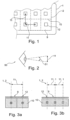
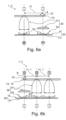
- Fig. 1 shows an enlarged section of a display device 1, in which the proportion of non-illuminating surfaces 9 in the entire display surface 2 is more than 70%.
- the centers of gravity of adjacent luminous surfaces 12 have mutual distances 11 that are smaller than the resolution of an observer.
- a very big advantage is that the luminous surfaces 12 are separated from one another by large separating areas, which are formed by non-luminous surfaces 9, and therefore on the one hand there is no scattered light from one luminous surface 12 to the other (or this is greatly reduced) and that On the other hand, dark areas of an image displayed by the display device 1 can appear even darker, since the non-luminous areas 9 predominate.
- Fig. 2 shows a purely qualitative illustration of a distance 11 which is smaller than the resolution of the viewer 50 and which appears to the viewer at an angle 51 of a maximum of two minutes of arc. At such a distance 11, most viewers 50 can no longer perceive two different pixels 10 and they therefore receive a particularly high-quality and continuous image impression.
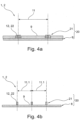
- FIG. 3a and 3b show excerpts from display devices 2 Fig. 1 wherein the display device 1 is a color display device. A side view is shown above a top view of the display surface 2. However, hatching is used here for better illustration and color differentiation. In Fig. 3a two pixels 10 are shown. A luminous area 12 is assigned to a pixel 10, with several colors being emitted to the viewer via the luminous area 12.
- composition of a pixel 10 Two possibilities for the composition of a pixel 10 are shown, on the left a composition of a pixel 10 from the colors red (close hatching from top left to bottom right), green (close hatching from bottom left to top right), blue (close hatching vertically) is preferred in a stripe arrangement and on the right from the colors red, green, blue and white (without hatching) preferably in an approximately square arrangement.
- Components with a wide hatching from top left to bottom left, such as the non-luminous surfaces 9 here, are preferably opaque.
- a pixel 10 is shown, to which three luminous areas 12 are assigned, red being able to be emitted to the viewer via a first luminous area 12, green via a second luminous area 12 and blue via a third luminous area 12.
- the distances 11.1 of the centroids of adjacent luminous areas 12 are 1/ 3 of the distance 11, which is smaller than the resolution of the viewer 50.
- Optical axes are each shown in dashed lines and in some cases a preferred lighting pattern or color of the corresponding light source 21 is indicated at the lower end of the axis and a preferred lighting pattern or color is indicated on the lighting surface 12 at the upper end of the axis.
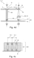
- Fig. 4a to 4e show excerpts of display devices 1 according to the invention Fig. 3a or 3b .
- the display device 1 has a lighting device 20 with a substrate 8 on which a plurality of light sources 21 are arranged, the light sources 21 preferably being small light sources 21 (e.g. VCSEL laser), ie preferably light sources 21 in which the surface area of the active luminous surface 22 is smaller or equal to the area of the corresponding luminous surface 12.
- Fig. 4a and 4d show Light sources 21 that are polychromatic, that is, that are set up to emit different, variable components of light with different wavelengths, for example red, green, blue components.
- Fig. 4b , 4c and 4e show light sources 21 that are monochromatic, ie that emit a non-variable wavelength range or a fixed mix of different wavelengths.
- the luminous surfaces 12 are each formed by one of the light sources 21.
- the non-luminous surfaces 9 of the display surface 2 are formed by surfaces of a filling material between the light sources 21, which is also the case Fig. 4b could be provided like this.
- the luminous surfaces 12 are each formed by one of the light sources 21.
- the non-luminous surfaces 9 of the display surface 2 are formed by surfaces of the substrate 8, which is also the case Fig. 4a could be provided like this.
- the active luminous surface 22 of the respective light source 21 is therefore also a luminous surface 12 of the display surface 2.
- a display device can thus be produced with just a few components, although very high-quality, bright and precisely measured light sources should advantageously be used for this purpose.
- the luminous surfaces 12 are each formed by a transparent cover element that can be illuminated by one of the light sources 21.
- the non-luminous surfaces 9 of the display surface 2 are formed by surfaces of a filling material between the light sources 21.
- Each light source 21 has a phosphor layer and an electron emitter, which is set up to cause the phosphor layer to actively glow by emitting an electron beam.
- the phosphor layer can also be viewed as a scattering element, as it distributes the incident radiation energy from one direction into several directions. There is a vacuum in a vacuum cell between the electron emitter and the phosphor layer.
- the advantage here is that, due to the inventive principle of a large intermediate surface between the luminous surfaces, a very good and economical sealing of the vacuum cells is also possible.
- Fig. 4d are the luminous surfaces 12 each by an optical scattering element 13 that can be illuminated by one of the light sources 21 (wide hatching from bottom left to top right - this type of hatching preferably means that the component hatched in this way, for example later lenses, is translucent, preferably essentially without color filtering , is) formed.
- the non-luminous surfaces 9 of the display surface 2 are formed by surfaces of a filling material between the light sources 21, at the level of the scattering elements 12. Two design options are shown, on the left with a so-called light guide (e.g a glass fiber) as a beam shaping device 30, which also serves as a concentrator 31, on the right with a lens as a concentrator 31.
- a so-called light guide e.g a glass fiber
- the resulting luminous pattern on the luminous surface 12 is as indicated above, on the left approximately the same size as the luminous pattern of the luminous surface 22, on the right slightly reduced .
- the resulting light pattern is more diffuse, preferably with colors mixed together, which occurs due to the scattering element 13, but cannot be represented advantageously in terms of drawing technology. This results in scattered radiation, but at the same time the light is concentrated onto the scattering elements 13.
- the luminous surfaces 12 are each formed by an optical color filter element 14 that can be illuminated by one of the light sources 21.
- the non-luminous surfaces 9 of the display surface 2 are formed by surfaces of a filling material between the light sources 21, at the level of the color filter elements 14.
- Each light source 21 has a UV emitter, which is set up to cause a phosphor layer, which here also acts as a scattering element 13, to actively glow by emitting a UV light beam.
- the different colors, here RGB are thus obtained through the color filter elements 14, for example through quantum dots.
- Three design options are also shown, left and right beam shaping elements 30 as in Fig. 4d and in the middle a variant without beam shaping element 30.
- Fig. 4d and 4e a collimator 34 part of the beam shaping device 30, analogous to e.g Fig. 6a .
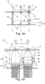
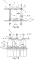
- FIG. 5a to 6d show excerpts of display devices 1 according to the invention Fig. 3a or 3b .
- These show in comparison Figs. 4a-4e larger light sources 21 and in particular optical beam shaping devices 30, which are arranged between the lighting device 20 and the display surface 2, and each beam shaping device 30 is assigned a luminous surface 12 and the beam shaping devices 30 are each set up to direct light from the lighting device 20 to the respective luminous surface 12 focus.
- the active luminous areas 22 of the light sources 21 each have an area that is larger than the respective area of the luminous area 12 of the display area 2.
- the display devices 1 each have optical beam shaping devices 30, which are arranged between the lighting device 20 and the display surface 2, and each beam shaping device 30 is assigned a luminous surface 12 and the beam shaping devices 30 are each set up to direct light from the lighting device 20 to the respective luminous surface 12 focus.
- the optical beam shaping devices 30 each have an optical collimator 34 (eg a semi-spherical collimator lens) and an optical concentrator 31 with curved ones Reflector surfaces and the optical collimator 34 is each arranged in front of the concentrator 31 with respect to a propagation direction of the light from the lighting device 20, so that light can initially be essentially collimated and then concentrated.
- a compound parabolic concentrator is provided as the concentrator 31 (represented by two opposite curved, preferably parabolically curved reflector surfaces and also in perspective Fig. 5c ), alternatively a condenser lens 31 (e.g Fig. 6a right).
- the collimators 34 are, on the one hand, prism collimators 34 (drawn by a pyramidal structure) or, alternatively, reflectors 34 (as in Fig. 6a to Fig. 6d ) available.
- the display devices 1 have light sources 21 that are approximately Lambert radiators.
- luminous surfaces 12 are each formed by an optical scattering element 13 that can be illuminated by the lighting device 20.
- the non-luminous surfaces 9 of the display surface 2 are formed by surfaces of a filling material arranged between the scattering elements 13, the filling material being shown here as a surface, but also being able to completely fill the space between adjacent beam shaping elements 30.
- the light sources are polychromatic and the light sources or their active luminous surfaces have an extent that is more than 50% of the distance 11 of the centers of gravity of the luminous surfaces 12.
- the CPCs 31 have an input 32 and an output 33 (see also Fig.
- the CPC has an optical input angle 37 which is a maximum of 30°-10°, preferably 20°, smaller than the optical output angle 36 of the prism collimator 34. Optical losses 35 can thus be minimized as much as possible.
- the combination of collimator 34 and concentrator 31 results in an effective concentration of light onto the luminous surfaces 12.
- the CPC as a non-imaging optic, achieves a very homogeneous color mixture, which is indicated by the white output light patterns.
- the scattering element 13 allows a large viewing angle.
- the beam path of the light is indicated by dashed arrows.
- Fig. 5b is a variant of the display device Fig. 5a shown, in which the extent of the light source 21 is less than 50% of the distance 11, but greater than the extent of the luminous surface 12.
- Fig. 5d are different from Fig. 5a the light sources are monochromatic and the luminous surfaces 12 are each formed by an optical color filter element that can be illuminated by the lighting device 20 and is at the same time a scattering element 13. Furthermore, there are distances 11.1 between the luminous surfaces 12, which amount to a third of the distance 11.
- the display devices 1 have light sources 21 which are the same size or larger than the luminous areas 12 in terms of area (for example based on the active luminous area of a light source). Otherwise it is Fig. 6a similar to Fig. 5a , where Fig. 6a in contrast to Fig. 5a Collimators 34 shows which surround the light sources 21 as a parabolic reflector. The optical collimator 34 is still arranged in front of the concentrator 31 with respect to a propagation direction of the light from the lighting device 20, so that light can first be essentially collimated and then concentrated.
- an RGBW light source is shown on the right and, instead of a CPC as a concentrator 31, a condenser lens, here a non-imaging condenser lens, which also brings about good homogenization of the light shining through the luminous surface 12.
- Fig. 6b is similar to Fig. 6a , wherein the light sources 21 are monochromatic and the luminous surfaces 12 are each formed by an optical color filter element that can be illuminated by the lighting device 20 and is at the same time a scattering element 13. Furthermore, there are distances 11.1 between the luminous surfaces 12, which amount to a third of the distance 11.
- Fig. 6c is similar to Fig.
- Fig. 6a wherein the light sources 21 are monochromatic, here white, and color filter elements 14 are arranged directly on the light sources 21. Furthermore, a design option with an imaging condenser lens 31 is shown on the right.
- Fig. 6d is similar to Fig. 6a , wherein the light sources 21 are monochromatic, here for example essentially emitting blue and/or UV.
- the luminous surfaces 12 are each formed by an optical color filter element 14 that can be illuminated by the lighting device 20.
- Each light source 21 has a blue and/or UV emitter, which is set up to cause a phosphor layer, which here also acts as a scattering element 13, to actively glow by emitting a blue and/or UV light beam.
- the different colors, here RGB are thus obtained through the color filter elements 14.
- Color filter elements 14 are arranged directly on the light sources 21 (eg quantum dots).
- Fig. 7 With reference to Fig. 7 becomes the description Fig. 1 referred, whereby Fig. 7 differs in that it additionally has functional elements 40.1.
- the functional elements 40.1 shown are arranged between the luminous surfaces 12 or on the non-illuminating surfaces 9.
- the arrangement and size of the functional elements 40.1 shown here is to be understood as an example.
- Functional elements 40.1 can be arranged in a repeating pattern, whereby a large number of areas between the luminous surfaces 12 are used can be.
- the size and shape of the functional elements 40.1 is also variable. Of course, any polygonal shape is also possible.
- the functional elements 40.1 shown can be, for example, a solar element and/or a sensor.
- a sensor can be, for example, a temperature sensor, a distance sensor, a pressure sensor, a gas sensor or an image sensor.
- a solar element is used to convert solar energy into electrical energy, which extends the energy supply to the display device by, for example, charging a battery or makes it possible in the first place.
- 8a and 8b differ only in the functional element 40.1, which is arranged on the non-luminous surface 9.
- the functional element 40.1 is attached to the top of the display surface 2. But it is also possible to arrange the functional elements 40.1 on the underside, i.e. on the side facing away from the viewer.
- the functional element 40.1 is designed as a piezo element, more precisely as a pressure sensor. An altimeter, for example, can be implemented using the pressure sensor. It is also possible to generate haptic feedback in the form of vibration with a piezo element.
- Fig. 9a a functional element 40.1 between two light sources 21 of the lighting device 20.
- the functional element 40.1 is arranged on the non-luminous surface 9 and designed as a gas sensor.
- Fig. 4d also meets the description of Fig. 9b to, whereby Fig. 9b is expanded by two functional elements 40.1 and 40.2. While a functional element 40.1 is arranged on the substrate 8 of the lighting device 20 between two light sources 21 and is designed as a capacitive sensor, the other functional element 40.2 forms a solar element. In order to enlarge the surface of the functional element 40.2 or the solar element and thus increase the energy yield, the functional element 40.2 has a polygonal shape. The polygon-shaped, triangular functional element 40.2 also forms the entire non-illuminating surface 9 of the display surface 2 between two luminous surfaces 12.
- the functional element can 40.2 only take up part of the non-illuminating area 9 of the display area 2.
- the beam shaping element 40.3 which is translucent and made of transparent material, is arranged between the luminous surfaces 12 and between the non-illuminating surfaces 9 and directs passing light onto the beam detector device 40.4 by refraction. In this way it is possible to realize a plenoptic camera, which can be formed by several functional elements 40.3 and 40.4. The available light of a scene, which hits the lens or the beam shaping element 40.3 from more than one direction, is thus imaged onto the beam detector device 40.4 or an image sensor.
- a plenoptic camera In contrast to a conventional camera, a plenoptic camera not only records the position and intensity of a light beam that hits an image sensor or the beam detector device 40.4, but also the direction from which the light beam is incident. A so-called light field measurement can thus be carried out. Consequently, it is using the design shown in Figure 9c , possible to arrange several lenses or beam shaping elements 40.3 in front of several image sensors or beam detector devices 40.4 in a simple manner.
- the advantages of a plenoptic camera are the high depth of field, no waiting for a focusing process and subsequent adjustment of the focal plane of a recorded object or image.
- the beam shaping element 40.3 is in Figure 9c arranged between two luminous surfaces 12 and designed in a hemispherical shape, but it can also have a different shape - depending on the application. So are e.g. B. polygonal shapes are also possible.
- the beam detector device 40.4 is arranged on the substrate 8 and between two light sources 21 and in the present case is a light field sensor which - as described above - detects the position and intensity, but also the direction of a light beam.
- An exemplary light beam is shown with an interrupted dashed line, which occurs on the beam shaping element 40.3, is refracted by it and further directed onto the beam detector device 40.4.
- a functional element 40.1 is arranged below the left non-luminous surface 9 of the display surface 2, the right non-luminous surface 9 being identical to that Figure 9b is designed.
- the polygon-shaped functional element 40.2 the description will be given for the sake of brevity Figure 9b referred to, which is also applicable here.
- the left functional element 40.1 is designed as a piezo element, which can generate haptic feedback and at the same time functions as a pressure sensor. This means that an input from a user can be detected on the display device 1 and at the same time haptic feedback can be generated for the input.
- the non-illuminating surfaces 9, preferably the entire display surface 2, preferably have a reflectance of diffuse reflection and/or specular reflection of less than 50%.
- the non-luminous surfaces 9 preferably have a dark color or are black and/or they have an average roughness in the range of 0.2 ⁇ m and 1.0 ⁇ m and/or are coated using an anti-reflective coating.
- An electronic compensation device is also preferably present, by means of which a minimum brightness of the luminous surfaces 12 can be automatically adjusted for adapting the display of black image pixels depending on the ambient brightness.
- This invention creates a revolutionary improvement in the quality of display devices.
- the image quality is increased by the principle of making the non-illuminating areas between the luminous areas as large as possible, for example by making the proportion of non-illuminating areas of the total display area at least 70%, as this improves the contrast and allows a lot of energy to be saved , which is particularly important for portable devices.
- special intensive light sources e.g.
- lasers or micro-LEDs or micro-OLEDS are used or special beam shaping devices, which are behind the display area as seen from the viewer, are used to concentrate light on the illuminated areas and thus A brightness boost is achieved so that the brightness average is similar to that of normal display devices, but with better contrast and lower energy consumption, depending on the ambient light.
Landscapes
- Physics & Mathematics (AREA)
- Optics & Photonics (AREA)
- General Physics & Mathematics (AREA)
- Nonlinear Science (AREA)
- Mathematical Physics (AREA)
- Chemical & Material Sciences (AREA)
- Crystallography & Structural Chemistry (AREA)
- Devices For Indicating Variable Information By Combining Individual Elements (AREA)
- Engineering & Computer Science (AREA)
- General Engineering & Computer Science (AREA)
- Microelectronics & Electronic Packaging (AREA)
- Electroluminescent Light Sources (AREA)
Applications Claiming Priority (4)
| Application Number | Priority Date | Filing Date | Title |
|---|---|---|---|
| DE102014002272 | 2014-02-19 | ||
| DE102014009677.7A DE102014009677A1 (de) | 2014-02-19 | 2014-06-30 | Anzeigevorrichtung mit verbessertem Kontrast |
| DE102014017764 | 2014-12-03 | ||
| PCT/EP2015/000355 WO2015124292A1 (de) | 2014-02-19 | 2015-02-18 | Anzeigevorrichtung |
Publications (3)
| Publication Number | Publication Date |
|---|---|
| EP3108286A1 EP3108286A1 (de) | 2016-12-28 |
| EP3108286C0 EP3108286C0 (de) | 2024-01-10 |
| EP3108286B1 true EP3108286B1 (de) | 2024-01-10 |
Family
ID=53877647
Family Applications (1)
| Application Number | Title | Priority Date | Filing Date |
|---|---|---|---|
| EP15705502.1A Active EP3108286B1 (de) | 2014-02-19 | 2015-02-18 | Anzeigevorrichtung |
Country Status (6)
| Country | Link |
|---|---|
| US (1) | US9951935B2 (enExample) |
| EP (1) | EP3108286B1 (enExample) |
| JP (1) | JP6535340B2 (enExample) |
| KR (1) | KR102329593B1 (enExample) |
| CN (1) | CN106030371B (enExample) |
| WO (1) | WO2015124292A1 (enExample) |
Families Citing this family (14)
| Publication number | Priority date | Publication date | Assignee | Title |
|---|---|---|---|---|
| US10847755B2 (en) * | 2016-03-02 | 2020-11-24 | Pa.Cotte Family Holding Gmbh | Method for producing a display device, and display device |
| EP3599644B1 (en) | 2018-07-26 | 2020-08-19 | PA.Cotte Family Holding GmbH | Multifunctional display |
| EP3599643B1 (en) | 2018-07-26 | 2020-08-19 | PA.Cotte Family Holding GmbH | Multifunctional display |
| CN109309738B (zh) * | 2018-08-01 | 2021-08-17 | 荣耀终端有限公司 | 接近光传感器组件及电子设备 |
| CN110808263B (zh) | 2018-08-06 | 2020-09-22 | 云谷(固安)科技有限公司 | 显示面板、显示屏及显示终端 |
| JP7110037B2 (ja) * | 2018-09-04 | 2022-08-01 | 株式会社ジャパンディスプレイ | 表示装置 |
| US11181775B2 (en) | 2018-09-11 | 2021-11-23 | Samsung Electronics Co., Ltd. | Illumination device and electronic apparatus including the same |
| KR20210052574A (ko) | 2018-10-01 | 2021-05-10 | 레이아 인코포레이티드 | 홀로그래픽 현실 시스템, 멀티뷰 디스플레이 및 방법 |
| TWI678010B (zh) * | 2018-12-07 | 2019-11-21 | 友達光電股份有限公司 | 顯示陣列面板及顯示裝置 |
| JP7320970B2 (ja) * | 2019-03-28 | 2023-08-04 | 株式会社ジャパンディスプレイ | 表示装置 |
| CN109935600B (zh) * | 2019-03-29 | 2021-03-30 | 京东方科技集团股份有限公司 | 一种Micro LED阵列结构、显示面板和显示装置 |
| CN111739428B (zh) * | 2020-07-23 | 2022-04-22 | 维沃移动通信有限公司 | 显示组件和显示装置 |
| DE102024113840A1 (de) | 2024-05-16 | 2025-11-20 | Alfred Kärcher SE & Co. KG | Reinigungsgerät |
| DE102024113789A1 (de) * | 2024-05-16 | 2025-11-20 | Alfred Kärcher SE & Co. KG | Anzeigevorrichtung für ein elektrisches Gerät und insbesondere Reinigungsgerät und Reinigungsgerät |
Citations (1)
| Publication number | Priority date | Publication date | Assignee | Title |
|---|---|---|---|---|
| US20040051447A1 (en) * | 2002-09-12 | 2004-03-18 | Canon Kabushiki Kaisha | Organic electroluminescent display and apparatus including organic electroluminescent display |
Family Cites Families (24)
| Publication number | Priority date | Publication date | Assignee | Title |
|---|---|---|---|---|
| EP0909972A3 (en) * | 1992-03-13 | 1999-06-09 | Kopin Corporation | Method of forming a high resolution liquid crystal display device |
| JPH1185056A (ja) * | 1997-09-10 | 1999-03-30 | Yazaki Corp | 多機能ディスプレイ装置 |
| US6476783B2 (en) * | 1998-02-17 | 2002-11-05 | Sarnoff Corporation | Contrast enhancement for an electronic display device by using a black matrix and lens array on outer surface of display |
| JP3952618B2 (ja) * | 1998-12-17 | 2007-08-01 | カシオ計算機株式会社 | 表示装置 |
| US6842170B1 (en) * | 1999-03-17 | 2005-01-11 | Motorola, Inc. | Display with aligned optical shutter and backlight cells applicable for use with a touchscreen |
| JP2002287900A (ja) * | 2000-12-12 | 2002-10-04 | Semiconductor Energy Lab Co Ltd | 情報装置 |
| WO2004019120A1 (en) * | 2002-08-21 | 2004-03-04 | Nokia Corporation | Switchable lens display |
| JP2004093602A (ja) * | 2002-08-29 | 2004-03-25 | Casio Comput Co Ltd | 太陽電池付き表示装置 |
| JP4886162B2 (ja) * | 2003-06-18 | 2012-02-29 | キヤノン株式会社 | 撮像装置付き表示装置 |
| GB2404774B (en) * | 2003-08-07 | 2007-02-14 | Pelikon Ltd | Electroluminescent displays |
| US7576915B2 (en) | 2003-12-17 | 2009-08-18 | Koninklijke Philips Electronics N.V. | Display device |
| US7884315B2 (en) | 2006-07-11 | 2011-02-08 | Apple Inc. | Invisible, light-transmissive display system |
| US7498735B2 (en) * | 2005-10-18 | 2009-03-03 | Eastman Kodak Company | OLED device having improved power distribution |
| KR100729047B1 (ko) * | 2005-12-21 | 2007-06-14 | 삼성에스디아이 주식회사 | 포토 다이오드를 구비하는 유기 발광 표시장치 |
| KR100821070B1 (ko) * | 2006-11-07 | 2008-04-08 | 삼성에스디아이 주식회사 | 포토 다이오드 및 이를 이용한 유기 전계 발광표시장치 |
| US8477125B2 (en) * | 2005-12-21 | 2013-07-02 | Samsung Display Co., Ltd. | Photo sensor and organic light-emitting display using the same |
| JP5162885B2 (ja) * | 2006-11-27 | 2013-03-13 | ソニー株式会社 | 面状光源装置及び液晶表示装置組立体 |
| US8128257B2 (en) * | 2007-02-09 | 2012-03-06 | Bright View Technologies Corporation | Curved compact collimating reflectors |
| WO2009098781A1 (ja) * | 2008-02-08 | 2009-08-13 | Fujitsu Limited | 表示装置および情報処理装置 |
| WO2011004841A1 (ja) * | 2009-07-10 | 2011-01-13 | シャープ株式会社 | タッチセンサ機能付き表示装置、及び集光遮光フィルム |
| US9870053B2 (en) * | 2010-02-08 | 2018-01-16 | Immersion Corporation | Systems and methods for haptic feedback using laterally driven piezoelectric actuators |
| TWI647973B (zh) * | 2011-02-11 | 2019-01-11 | Semiconductor Energy Laboratory Co., Ltd. | 發光元件、發光裝置以及顯示裝置 |
| WO2013117760A1 (en) * | 2012-02-10 | 2013-08-15 | University College Cork, National University Of Ireland, Cork | Light emitting diode chip |
| US20130321373A1 (en) * | 2012-05-31 | 2013-12-05 | Semiconductor Energy Laboratory Co., Ltd. | Electronic device, program, and recording medium |
-
2015
- 2015-02-18 WO PCT/EP2015/000355 patent/WO2015124292A1/de not_active Ceased
- 2015-02-18 CN CN201580009664.7A patent/CN106030371B/zh active Active
- 2015-02-18 JP JP2016552639A patent/JP6535340B2/ja active Active
- 2015-02-18 EP EP15705502.1A patent/EP3108286B1/de active Active
- 2015-02-18 US US15/119,628 patent/US9951935B2/en active Active
- 2015-02-18 KR KR1020167025544A patent/KR102329593B1/ko active Active
Patent Citations (1)
| Publication number | Priority date | Publication date | Assignee | Title |
|---|---|---|---|---|
| US20040051447A1 (en) * | 2002-09-12 | 2004-03-18 | Canon Kabushiki Kaisha | Organic electroluminescent display and apparatus including organic electroluminescent display |
Also Published As
| Publication number | Publication date |
|---|---|
| CN106030371B (zh) | 2020-05-05 |
| US20170082273A1 (en) | 2017-03-23 |
| EP3108286A1 (de) | 2016-12-28 |
| WO2015124292A1 (de) | 2015-08-27 |
| JP2017511898A (ja) | 2017-04-27 |
| KR20160122831A (ko) | 2016-10-24 |
| EP3108286C0 (de) | 2024-01-10 |
| JP6535340B2 (ja) | 2019-06-26 |
| KR102329593B1 (ko) | 2021-11-19 |
| CN106030371A (zh) | 2016-10-12 |
| US9951935B2 (en) | 2018-04-24 |
Similar Documents
| Publication | Publication Date | Title |
|---|---|---|
| EP3108286B1 (de) | Anzeigevorrichtung | |
| EP3108285B1 (de) | Anzeigevorrichtung mit verbessertem kontrast | |
| DE112018004945B4 (de) | Head-up-display-vorrichtung und bildprojektionseinheit | |
| DE69723542T2 (de) | Bildsensor | |
| US8941800B2 (en) | Reflective image forming element and optical system | |
| DE102006030541B4 (de) | Optische Anordnung | |
| DE112010003742T5 (de) | Hochschnelles, hochauflösendes, dreidimensionales Solarzellenprüfsystem | |
| EP3440503A1 (de) | Bildschrirm fuer einen freien und einen eingeschraenkten sichtmodus | |
| DE102006023694A1 (de) | Planarlichtquellenvorrichtung und Anzeigevorrichtung, welche dieselbe verwendet | |
| DE112012002308T5 (de) | Hintergrundbeleuchtung und Flüssigkristallanzeigevorrichtung | |
| WO2010081652A1 (de) | Vorrichtung zur optischen navigation | |
| DE112019005191T5 (de) | Bildanzeigevorrichtung | |
| DE102014017281A1 (de) | Optische Detektionsvorrichtung und Verfahren zum Steuern derselben | |
| EP2003443A1 (de) | Vorrichtung zum Erfassen eines Bildes | |
| DE112020004339T5 (de) | Lichtquellenvorrichtung und informationsanzeigesystem, das selbige verwendet | |
| DE102018105569A1 (de) | Leuchteinrichtung | |
| EP3327494A1 (de) | Doppelseitiger bildschirm mit gemeinsamem backlight | |
| DE19623881A1 (de) | Elektrolumineszenzdisplay | |
| DE102008055714B4 (de) | Semitransparente Beleuchtungsvorrichtung | |
| DE112021004550T5 (de) | Bildanzeigevorrichtung und elektronische einrichtung | |
| US20240180007A1 (en) | Display panel and display device | |
| DE602004001633T2 (de) | Lichtleiterplatte, Beleuchtungsvorrichtung und Flüssigkristallanzeige | |
| DE10164033A1 (de) | Optoelektronisches Bauelement | |
| DE202011051449U1 (de) | Waage | |
| DE102014117317A1 (de) | Display-Vorrichtung, Verfahren zum Herstellen einer Display-Vorrichtung und Verfahren zum Betreiben einer Display-Vorrichtung |
Legal Events
| Date | Code | Title | Description |
|---|---|---|---|
| PUAI | Public reference made under article 153(3) epc to a published international application that has entered the european phase |
Free format text: ORIGINAL CODE: 0009012 |
|
| STAA | Information on the status of an ep patent application or granted ep patent |
Free format text: STATUS: REQUEST FOR EXAMINATION WAS MADE |
|
| 17P | Request for examination filed |
Effective date: 20160919 |
|
| AK | Designated contracting states |
Kind code of ref document: A1 Designated state(s): AL AT BE BG CH CY CZ DE DK EE ES FI FR GB GR HR HU IE IS IT LI LT LU LV MC MK MT NL NO PL PT RO RS SE SI SK SM TR |
|
| AX | Request for extension of the european patent |
Extension state: BA ME |
|
| DAX | Request for extension of the european patent (deleted) | ||
| STAA | Information on the status of an ep patent application or granted ep patent |
Free format text: STATUS: EXAMINATION IS IN PROGRESS |
|
| 17Q | First examination report despatched |
Effective date: 20191218 |
|
| GRAP | Despatch of communication of intention to grant a patent |
Free format text: ORIGINAL CODE: EPIDOSNIGR1 |
|
| STAA | Information on the status of an ep patent application or granted ep patent |
Free format text: STATUS: GRANT OF PATENT IS INTENDED |
|
| RIC1 | Information provided on ipc code assigned before grant |
Ipc: G02F 1/1335 20060101ALI20230821BHEP Ipc: H10K 50/00 20230101ALI20230821BHEP Ipc: G02B 26/02 20060101AFI20230821BHEP |
|
| INTG | Intention to grant announced |
Effective date: 20230912 |
|
| GRAS | Grant fee paid |
Free format text: ORIGINAL CODE: EPIDOSNIGR3 |
|
| GRAA | (expected) grant |
Free format text: ORIGINAL CODE: 0009210 |
|
| STAA | Information on the status of an ep patent application or granted ep patent |
Free format text: STATUS: THE PATENT HAS BEEN GRANTED |
|
| AK | Designated contracting states |
Kind code of ref document: B1 Designated state(s): AL AT BE BG CH CY CZ DE DK EE ES FI FR GB GR HR HU IE IS IT LI LT LU LV MC MK MT NL NO PL PT RO RS SE SI SK SM TR |
|
| REG | Reference to a national code |
Ref country code: GB Ref legal event code: FG4D Free format text: NOT ENGLISH |
|
| REG | Reference to a national code |
Ref country code: CH Ref legal event code: EP |
|
| REG | Reference to a national code |
Ref country code: DE Ref legal event code: R096 Ref document number: 502015016730 Country of ref document: DE |
|
| REG | Reference to a national code |
Ref country code: IE Ref legal event code: FG4D Free format text: LANGUAGE OF EP DOCUMENT: GERMAN |
|
| U01 | Request for unitary effect filed |
Effective date: 20240122 |
|
| U07 | Unitary effect registered |
Designated state(s): AT BE BG DE DK EE FI FR IT LT LU LV MT NL PT SE SI Effective date: 20240129 |
|
| U20 | Renewal fee for the european patent with unitary effect paid |
Year of fee payment: 10 Effective date: 20240221 |
|
| PG25 | Lapsed in a contracting state [announced via postgrant information from national office to epo] |
Ref country code: IS Free format text: LAPSE BECAUSE OF FAILURE TO SUBMIT A TRANSLATION OF THE DESCRIPTION OR TO PAY THE FEE WITHIN THE PRESCRIBED TIME-LIMIT Effective date: 20240510 |
|
| PG25 | Lapsed in a contracting state [announced via postgrant information from national office to epo] |
Ref country code: GR Free format text: LAPSE BECAUSE OF FAILURE TO SUBMIT A TRANSLATION OF THE DESCRIPTION OR TO PAY THE FEE WITHIN THE PRESCRIBED TIME-LIMIT Effective date: 20240411 |
|
| PG25 | Lapsed in a contracting state [announced via postgrant information from national office to epo] |
Ref country code: HR Free format text: LAPSE BECAUSE OF FAILURE TO SUBMIT A TRANSLATION OF THE DESCRIPTION OR TO PAY THE FEE WITHIN THE PRESCRIBED TIME-LIMIT Effective date: 20240110 Ref country code: RS Free format text: LAPSE BECAUSE OF FAILURE TO SUBMIT A TRANSLATION OF THE DESCRIPTION OR TO PAY THE FEE WITHIN THE PRESCRIBED TIME-LIMIT Effective date: 20240410 |
|
| PG25 | Lapsed in a contracting state [announced via postgrant information from national office to epo] |
Ref country code: ES Free format text: LAPSE BECAUSE OF FAILURE TO SUBMIT A TRANSLATION OF THE DESCRIPTION OR TO PAY THE FEE WITHIN THE PRESCRIBED TIME-LIMIT Effective date: 20240110 |
|
| PG25 | Lapsed in a contracting state [announced via postgrant information from national office to epo] |
Ref country code: RS Free format text: LAPSE BECAUSE OF FAILURE TO SUBMIT A TRANSLATION OF THE DESCRIPTION OR TO PAY THE FEE WITHIN THE PRESCRIBED TIME-LIMIT Effective date: 20240410 Ref country code: NO Free format text: LAPSE BECAUSE OF FAILURE TO SUBMIT A TRANSLATION OF THE DESCRIPTION OR TO PAY THE FEE WITHIN THE PRESCRIBED TIME-LIMIT Effective date: 20240410 Ref country code: IS Free format text: LAPSE BECAUSE OF FAILURE TO SUBMIT A TRANSLATION OF THE DESCRIPTION OR TO PAY THE FEE WITHIN THE PRESCRIBED TIME-LIMIT Effective date: 20240510 Ref country code: HR Free format text: LAPSE BECAUSE OF FAILURE TO SUBMIT A TRANSLATION OF THE DESCRIPTION OR TO PAY THE FEE WITHIN THE PRESCRIBED TIME-LIMIT Effective date: 20240110 Ref country code: GR Free format text: LAPSE BECAUSE OF FAILURE TO SUBMIT A TRANSLATION OF THE DESCRIPTION OR TO PAY THE FEE WITHIN THE PRESCRIBED TIME-LIMIT Effective date: 20240411 Ref country code: ES Free format text: LAPSE BECAUSE OF FAILURE TO SUBMIT A TRANSLATION OF THE DESCRIPTION OR TO PAY THE FEE WITHIN THE PRESCRIBED TIME-LIMIT Effective date: 20240110 |
|
| PG25 | Lapsed in a contracting state [announced via postgrant information from national office to epo] |
Ref country code: PL Free format text: LAPSE BECAUSE OF FAILURE TO SUBMIT A TRANSLATION OF THE DESCRIPTION OR TO PAY THE FEE WITHIN THE PRESCRIBED TIME-LIMIT Effective date: 20240110 |
|
| PG25 | Lapsed in a contracting state [announced via postgrant information from national office to epo] |
Ref country code: PL Free format text: LAPSE BECAUSE OF FAILURE TO SUBMIT A TRANSLATION OF THE DESCRIPTION OR TO PAY THE FEE WITHIN THE PRESCRIBED TIME-LIMIT Effective date: 20240110 |
|
| REG | Reference to a national code |
Ref country code: DE Ref legal event code: R097 Ref document number: 502015016730 Country of ref document: DE |
|
| PG25 | Lapsed in a contracting state [announced via postgrant information from national office to epo] |
Ref country code: SM Free format text: LAPSE BECAUSE OF FAILURE TO SUBMIT A TRANSLATION OF THE DESCRIPTION OR TO PAY THE FEE WITHIN THE PRESCRIBED TIME-LIMIT Effective date: 20240110 |
|
| PG25 | Lapsed in a contracting state [announced via postgrant information from national office to epo] |
Ref country code: CZ Free format text: LAPSE BECAUSE OF FAILURE TO SUBMIT A TRANSLATION OF THE DESCRIPTION OR TO PAY THE FEE WITHIN THE PRESCRIBED TIME-LIMIT Effective date: 20240110 |
|
| PG25 | Lapsed in a contracting state [announced via postgrant information from national office to epo] |
Ref country code: SK Free format text: LAPSE BECAUSE OF FAILURE TO SUBMIT A TRANSLATION OF THE DESCRIPTION OR TO PAY THE FEE WITHIN THE PRESCRIBED TIME-LIMIT Effective date: 20240110 |
|
| PG25 | Lapsed in a contracting state [announced via postgrant information from national office to epo] |
Ref country code: SM Free format text: LAPSE BECAUSE OF FAILURE TO SUBMIT A TRANSLATION OF THE DESCRIPTION OR TO PAY THE FEE WITHIN THE PRESCRIBED TIME-LIMIT Effective date: 20240110 Ref country code: SK Free format text: LAPSE BECAUSE OF FAILURE TO SUBMIT A TRANSLATION OF THE DESCRIPTION OR TO PAY THE FEE WITHIN THE PRESCRIBED TIME-LIMIT Effective date: 20240110 Ref country code: RO Free format text: LAPSE BECAUSE OF FAILURE TO SUBMIT A TRANSLATION OF THE DESCRIPTION OR TO PAY THE FEE WITHIN THE PRESCRIBED TIME-LIMIT Effective date: 20240110 Ref country code: CZ Free format text: LAPSE BECAUSE OF FAILURE TO SUBMIT A TRANSLATION OF THE DESCRIPTION OR TO PAY THE FEE WITHIN THE PRESCRIBED TIME-LIMIT Effective date: 20240110 |
|
| PG25 | Lapsed in a contracting state [announced via postgrant information from national office to epo] |
Ref country code: MC Free format text: LAPSE BECAUSE OF FAILURE TO SUBMIT A TRANSLATION OF THE DESCRIPTION OR TO PAY THE FEE WITHIN THE PRESCRIBED TIME-LIMIT Effective date: 20240110 |
|
| PLBE | No opposition filed within time limit |
Free format text: ORIGINAL CODE: 0009261 |
|
| STAA | Information on the status of an ep patent application or granted ep patent |
Free format text: STATUS: NO OPPOSITION FILED WITHIN TIME LIMIT |
|
| PG25 | Lapsed in a contracting state [announced via postgrant information from national office to epo] |
Ref country code: MC Free format text: LAPSE BECAUSE OF FAILURE TO SUBMIT A TRANSLATION OF THE DESCRIPTION OR TO PAY THE FEE WITHIN THE PRESCRIBED TIME-LIMIT Effective date: 20240110 |
|
| 26N | No opposition filed |
Effective date: 20241011 |
|
| U20 | Renewal fee for the european patent with unitary effect paid |
Year of fee payment: 11 Effective date: 20241216 |
|
| PG25 | Lapsed in a contracting state [announced via postgrant information from national office to epo] |
Ref country code: IE Free format text: LAPSE BECAUSE OF NON-PAYMENT OF DUE FEES Effective date: 20240218 |
|
| PG25 | Lapsed in a contracting state [announced via postgrant information from national office to epo] |
Ref country code: IE Free format text: LAPSE BECAUSE OF NON-PAYMENT OF DUE FEES Effective date: 20240218 |
|
| PG25 | Lapsed in a contracting state [announced via postgrant information from national office to epo] |
Ref country code: CY Free format text: LAPSE BECAUSE OF FAILURE TO SUBMIT A TRANSLATION OF THE DESCRIPTION OR TO PAY THE FEE WITHIN THE PRESCRIBED TIME-LIMIT; INVALID AB INITIO Effective date: 20150218 |
|
| PG25 | Lapsed in a contracting state [announced via postgrant information from national office to epo] |
Ref country code: HU Free format text: LAPSE BECAUSE OF FAILURE TO SUBMIT A TRANSLATION OF THE DESCRIPTION OR TO PAY THE FEE WITHIN THE PRESCRIBED TIME-LIMIT; INVALID AB INITIO Effective date: 20150218 |
|
| PG25 | Lapsed in a contracting state [announced via postgrant information from national office to epo] |
Ref country code: TR Free format text: LAPSE BECAUSE OF FAILURE TO SUBMIT A TRANSLATION OF THE DESCRIPTION OR TO PAY THE FEE WITHIN THE PRESCRIBED TIME-LIMIT Effective date: 20240110 |
|
| U20 | Renewal fee for the european patent with unitary effect paid |
Year of fee payment: 12 Effective date: 20251218 |
|
| REG | Reference to a national code |
Ref country code: CH Ref legal event code: U11 Free format text: ST27 STATUS EVENT CODE: U-0-0-U10-U11 (AS PROVIDED BY THE NATIONAL OFFICE) Effective date: 20260301 |
|
| PGFP | Annual fee paid to national office [announced via postgrant information from national office to epo] |
Ref country code: GB Payment date: 20260219 Year of fee payment: 12 |
|
| PGFP | Annual fee paid to national office [announced via postgrant information from national office to epo] |
Ref country code: CH Payment date: 20260301 Year of fee payment: 12 |