EP3107128B1 - Preparation method of a non-polar blue led epitaxial wafer based on lao substrate - Google Patents
Preparation method of a non-polar blue led epitaxial wafer based on lao substrate Download PDFInfo
- Publication number
- EP3107128B1 EP3107128B1 EP15769396.1A EP15769396A EP3107128B1 EP 3107128 B1 EP3107128 B1 EP 3107128B1 EP 15769396 A EP15769396 A EP 15769396A EP 3107128 B1 EP3107128 B1 EP 3107128B1
- Authority
- EP
- European Patent Office
- Prior art keywords
- polar
- lao substrate
- range
- layer
- lao
- Prior art date
- Legal status (The legal status is an assumption and is not a legal conclusion. Google has not performed a legal analysis and makes no representation as to the accuracy of the status listed.)
- Active
Links
Images

Classifications
-
- H—ELECTRICITY
- H10—SEMICONDUCTOR DEVICES; ELECTRIC SOLID-STATE DEVICES NOT OTHERWISE PROVIDED FOR
- H10H—INORGANIC LIGHT-EMITTING SEMICONDUCTOR DEVICES HAVING POTENTIAL BARRIERS
- H10H20/00—Individual inorganic light-emitting semiconductor devices having potential barriers, e.g. light-emitting diodes [LED]
- H10H20/01—Manufacture or treatment
-
- C—CHEMISTRY; METALLURGY
- C30—CRYSTAL GROWTH
- C30B—SINGLE-CRYSTAL GROWTH; UNIDIRECTIONAL SOLIDIFICATION OF EUTECTIC MATERIAL OR UNIDIRECTIONAL DEMIXING OF EUTECTOID MATERIAL; REFINING BY ZONE-MELTING OF MATERIAL; PRODUCTION OF A HOMOGENEOUS POLYCRYSTALLINE MATERIAL WITH DEFINED STRUCTURE; SINGLE CRYSTALS OR HOMOGENEOUS POLYCRYSTALLINE MATERIAL WITH DEFINED STRUCTURE; AFTER-TREATMENT OF SINGLE CRYSTALS OR A HOMOGENEOUS POLYCRYSTALLINE MATERIAL WITH DEFINED STRUCTURE; APPARATUS THEREFOR
- C30B11/00—Single-crystal growth by normal freezing or freezing under temperature gradient, e.g. Bridgman-Stockbarger method
- C30B11/14—Single-crystal growth by normal freezing or freezing under temperature gradient, e.g. Bridgman-Stockbarger method characterised by the seed, e.g. its crystallographic orientation
-
- C—CHEMISTRY; METALLURGY
- C30—CRYSTAL GROWTH
- C30B—SINGLE-CRYSTAL GROWTH; UNIDIRECTIONAL SOLIDIFICATION OF EUTECTIC MATERIAL OR UNIDIRECTIONAL DEMIXING OF EUTECTOID MATERIAL; REFINING BY ZONE-MELTING OF MATERIAL; PRODUCTION OF A HOMOGENEOUS POLYCRYSTALLINE MATERIAL WITH DEFINED STRUCTURE; SINGLE CRYSTALS OR HOMOGENEOUS POLYCRYSTALLINE MATERIAL WITH DEFINED STRUCTURE; AFTER-TREATMENT OF SINGLE CRYSTALS OR A HOMOGENEOUS POLYCRYSTALLINE MATERIAL WITH DEFINED STRUCTURE; APPARATUS THEREFOR
- C30B23/00—Single-crystal growth by condensing evaporated or sublimed materials
- C30B23/02—Epitaxial-layer growth
- C30B23/025—Epitaxial-layer growth characterised by the substrate
-
- C—CHEMISTRY; METALLURGY
- C30—CRYSTAL GROWTH
- C30B—SINGLE-CRYSTAL GROWTH; UNIDIRECTIONAL SOLIDIFICATION OF EUTECTIC MATERIAL OR UNIDIRECTIONAL DEMIXING OF EUTECTOID MATERIAL; REFINING BY ZONE-MELTING OF MATERIAL; PRODUCTION OF A HOMOGENEOUS POLYCRYSTALLINE MATERIAL WITH DEFINED STRUCTURE; SINGLE CRYSTALS OR HOMOGENEOUS POLYCRYSTALLINE MATERIAL WITH DEFINED STRUCTURE; AFTER-TREATMENT OF SINGLE CRYSTALS OR A HOMOGENEOUS POLYCRYSTALLINE MATERIAL WITH DEFINED STRUCTURE; APPARATUS THEREFOR
- C30B25/00—Single-crystal growth by chemical reaction of reactive gases, e.g. chemical vapour-deposition growth
- C30B25/02—Epitaxial-layer growth
- C30B25/18—Epitaxial-layer growth characterised by the substrate
-
- C—CHEMISTRY; METALLURGY
- C30—CRYSTAL GROWTH
- C30B—SINGLE-CRYSTAL GROWTH; UNIDIRECTIONAL SOLIDIFICATION OF EUTECTIC MATERIAL OR UNIDIRECTIONAL DEMIXING OF EUTECTOID MATERIAL; REFINING BY ZONE-MELTING OF MATERIAL; PRODUCTION OF A HOMOGENEOUS POLYCRYSTALLINE MATERIAL WITH DEFINED STRUCTURE; SINGLE CRYSTALS OR HOMOGENEOUS POLYCRYSTALLINE MATERIAL WITH DEFINED STRUCTURE; AFTER-TREATMENT OF SINGLE CRYSTALS OR A HOMOGENEOUS POLYCRYSTALLINE MATERIAL WITH DEFINED STRUCTURE; APPARATUS THEREFOR
- C30B25/00—Single-crystal growth by chemical reaction of reactive gases, e.g. chemical vapour-deposition growth
- C30B25/02—Epitaxial-layer growth
- C30B25/18—Epitaxial-layer growth characterised by the substrate
- C30B25/183—Epitaxial-layer growth characterised by the substrate being provided with a buffer layer, e.g. a lattice matching layer
-
- C—CHEMISTRY; METALLURGY
- C30—CRYSTAL GROWTH
- C30B—SINGLE-CRYSTAL GROWTH; UNIDIRECTIONAL SOLIDIFICATION OF EUTECTIC MATERIAL OR UNIDIRECTIONAL DEMIXING OF EUTECTOID MATERIAL; REFINING BY ZONE-MELTING OF MATERIAL; PRODUCTION OF A HOMOGENEOUS POLYCRYSTALLINE MATERIAL WITH DEFINED STRUCTURE; SINGLE CRYSTALS OR HOMOGENEOUS POLYCRYSTALLINE MATERIAL WITH DEFINED STRUCTURE; AFTER-TREATMENT OF SINGLE CRYSTALS OR A HOMOGENEOUS POLYCRYSTALLINE MATERIAL WITH DEFINED STRUCTURE; APPARATUS THEREFOR
- C30B25/00—Single-crystal growth by chemical reaction of reactive gases, e.g. chemical vapour-deposition growth
- C30B25/02—Epitaxial-layer growth
- C30B25/18—Epitaxial-layer growth characterised by the substrate
- C30B25/186—Epitaxial-layer growth characterised by the substrate being specially pre-treated by, e.g. chemical or physical means
-
- C—CHEMISTRY; METALLURGY
- C30—CRYSTAL GROWTH
- C30B—SINGLE-CRYSTAL GROWTH; UNIDIRECTIONAL SOLIDIFICATION OF EUTECTIC MATERIAL OR UNIDIRECTIONAL DEMIXING OF EUTECTOID MATERIAL; REFINING BY ZONE-MELTING OF MATERIAL; PRODUCTION OF A HOMOGENEOUS POLYCRYSTALLINE MATERIAL WITH DEFINED STRUCTURE; SINGLE CRYSTALS OR HOMOGENEOUS POLYCRYSTALLINE MATERIAL WITH DEFINED STRUCTURE; AFTER-TREATMENT OF SINGLE CRYSTALS OR A HOMOGENEOUS POLYCRYSTALLINE MATERIAL WITH DEFINED STRUCTURE; APPARATUS THEREFOR
- C30B29/00—Single crystals or homogeneous polycrystalline material with defined structure characterised by the material or by their shape
- C30B29/10—Inorganic compounds or compositions
- C30B29/40—AIIIBV compounds wherein A is B, Al, Ga, In or Tl and B is N, P, As, Sb or Bi
- C30B29/403—AIII-nitrides
-
- C—CHEMISTRY; METALLURGY
- C30—CRYSTAL GROWTH
- C30B—SINGLE-CRYSTAL GROWTH; UNIDIRECTIONAL SOLIDIFICATION OF EUTECTIC MATERIAL OR UNIDIRECTIONAL DEMIXING OF EUTECTOID MATERIAL; REFINING BY ZONE-MELTING OF MATERIAL; PRODUCTION OF A HOMOGENEOUS POLYCRYSTALLINE MATERIAL WITH DEFINED STRUCTURE; SINGLE CRYSTALS OR HOMOGENEOUS POLYCRYSTALLINE MATERIAL WITH DEFINED STRUCTURE; AFTER-TREATMENT OF SINGLE CRYSTALS OR A HOMOGENEOUS POLYCRYSTALLINE MATERIAL WITH DEFINED STRUCTURE; APPARATUS THEREFOR
- C30B29/00—Single crystals or homogeneous polycrystalline material with defined structure characterised by the material or by their shape
- C30B29/10—Inorganic compounds or compositions
- C30B29/40—AIIIBV compounds wherein A is B, Al, Ga, In or Tl and B is N, P, As, Sb or Bi
- C30B29/403—AIII-nitrides
- C30B29/406—Gallium nitride
-
- H—ELECTRICITY
- H10—SEMICONDUCTOR DEVICES; ELECTRIC SOLID-STATE DEVICES NOT OTHERWISE PROVIDED FOR
- H10H—INORGANIC LIGHT-EMITTING SEMICONDUCTOR DEVICES HAVING POTENTIAL BARRIERS
- H10H20/00—Individual inorganic light-emitting semiconductor devices having potential barriers, e.g. light-emitting diodes [LED]
- H10H20/01—Manufacture or treatment
- H10H20/011—Manufacture or treatment of bodies, e.g. forming semiconductor layers
- H10H20/013—Manufacture or treatment of bodies, e.g. forming semiconductor layers having light-emitting regions comprising only Group III-V materials
- H10H20/0133—Manufacture or treatment of bodies, e.g. forming semiconductor layers having light-emitting regions comprising only Group III-V materials with a substrate not being Group III-V materials
- H10H20/01335—Manufacture or treatment of bodies, e.g. forming semiconductor layers having light-emitting regions comprising only Group III-V materials with a substrate not being Group III-V materials the light-emitting regions comprising nitride materials
-
- H—ELECTRICITY
- H10—SEMICONDUCTOR DEVICES; ELECTRIC SOLID-STATE DEVICES NOT OTHERWISE PROVIDED FOR
- H10H—INORGANIC LIGHT-EMITTING SEMICONDUCTOR DEVICES HAVING POTENTIAL BARRIERS
- H10H20/00—Individual inorganic light-emitting semiconductor devices having potential barriers, e.g. light-emitting diodes [LED]
- H10H20/80—Constructional details
- H10H20/81—Bodies
-
- H—ELECTRICITY
- H10—SEMICONDUCTOR DEVICES; ELECTRIC SOLID-STATE DEVICES NOT OTHERWISE PROVIDED FOR
- H10H—INORGANIC LIGHT-EMITTING SEMICONDUCTOR DEVICES HAVING POTENTIAL BARRIERS
- H10H20/00—Individual inorganic light-emitting semiconductor devices having potential barriers, e.g. light-emitting diodes [LED]
- H10H20/80—Constructional details
- H10H20/81—Bodies
- H10H20/811—Bodies having quantum effect structures or superlattices, e.g. tunnel junctions
-
- H—ELECTRICITY
- H10—SEMICONDUCTOR DEVICES; ELECTRIC SOLID-STATE DEVICES NOT OTHERWISE PROVIDED FOR
- H10H—INORGANIC LIGHT-EMITTING SEMICONDUCTOR DEVICES HAVING POTENTIAL BARRIERS
- H10H20/00—Individual inorganic light-emitting semiconductor devices having potential barriers, e.g. light-emitting diodes [LED]
- H10H20/80—Constructional details
- H10H20/81—Bodies
- H10H20/811—Bodies having quantum effect structures or superlattices, e.g. tunnel junctions
- H10H20/812—Bodies having quantum effect structures or superlattices, e.g. tunnel junctions within the light-emitting regions, e.g. having quantum confinement structures
-
- H—ELECTRICITY
- H10—SEMICONDUCTOR DEVICES; ELECTRIC SOLID-STATE DEVICES NOT OTHERWISE PROVIDED FOR
- H10H—INORGANIC LIGHT-EMITTING SEMICONDUCTOR DEVICES HAVING POTENTIAL BARRIERS
- H10H20/00—Individual inorganic light-emitting semiconductor devices having potential barriers, e.g. light-emitting diodes [LED]
- H10H20/80—Constructional details
- H10H20/81—Bodies
- H10H20/815—Bodies having stress relaxation structures, e.g. buffer layers
-
- H—ELECTRICITY
- H10—SEMICONDUCTOR DEVICES; ELECTRIC SOLID-STATE DEVICES NOT OTHERWISE PROVIDED FOR
- H10H—INORGANIC LIGHT-EMITTING SEMICONDUCTOR DEVICES HAVING POTENTIAL BARRIERS
- H10H20/00—Individual inorganic light-emitting semiconductor devices having potential barriers, e.g. light-emitting diodes [LED]
- H10H20/80—Constructional details
- H10H20/81—Bodies
- H10H20/816—Bodies having carrier transport control structures, e.g. highly-doped semiconductor layers or current-blocking structures
- H10H20/8162—Current-blocking structures
-
- H—ELECTRICITY
- H10—SEMICONDUCTOR DEVICES; ELECTRIC SOLID-STATE DEVICES NOT OTHERWISE PROVIDED FOR
- H10H—INORGANIC LIGHT-EMITTING SEMICONDUCTOR DEVICES HAVING POTENTIAL BARRIERS
- H10H20/00—Individual inorganic light-emitting semiconductor devices having potential barriers, e.g. light-emitting diodes [LED]
- H10H20/80—Constructional details
- H10H20/81—Bodies
- H10H20/822—Materials of the light-emitting regions
- H10H20/824—Materials of the light-emitting regions comprising only Group III-V materials, e.g. GaP
- H10H20/825—Materials of the light-emitting regions comprising only Group III-V materials, e.g. GaP containing nitrogen, e.g. GaN
-
- H—ELECTRICITY
- H10—SEMICONDUCTOR DEVICES; ELECTRIC SOLID-STATE DEVICES NOT OTHERWISE PROVIDED FOR
- H10P—GENERIC PROCESSES OR APPARATUS FOR THE MANUFACTURE OR TREATMENT OF DEVICES COVERED BY CLASS H10
- H10P14/00—Formation of materials, e.g. in the shape of layers or pillars
- H10P14/20—Formation of materials, e.g. in the shape of layers or pillars of semiconductor materials
- H10P14/24—Formation of materials, e.g. in the shape of layers or pillars of semiconductor materials using chemical vapour deposition [CVD]
-
- H—ELECTRICITY
- H10—SEMICONDUCTOR DEVICES; ELECTRIC SOLID-STATE DEVICES NOT OTHERWISE PROVIDED FOR
- H10P—GENERIC PROCESSES OR APPARATUS FOR THE MANUFACTURE OR TREATMENT OF DEVICES COVERED BY CLASS H10
- H10P14/00—Formation of materials, e.g. in the shape of layers or pillars
- H10P14/20—Formation of materials, e.g. in the shape of layers or pillars of semiconductor materials
- H10P14/29—Formation of materials, e.g. in the shape of layers or pillars of semiconductor materials characterised by the substrates
- H10P14/2901—Materials
- H10P14/2918—Materials being semiconductor metal oxides
-
- H—ELECTRICITY
- H10—SEMICONDUCTOR DEVICES; ELECTRIC SOLID-STATE DEVICES NOT OTHERWISE PROVIDED FOR
- H10P—GENERIC PROCESSES OR APPARATUS FOR THE MANUFACTURE OR TREATMENT OF DEVICES COVERED BY CLASS H10
- H10P14/00—Formation of materials, e.g. in the shape of layers or pillars
- H10P14/20—Formation of materials, e.g. in the shape of layers or pillars of semiconductor materials
- H10P14/29—Formation of materials, e.g. in the shape of layers or pillars of semiconductor materials characterised by the substrates
- H10P14/2901—Materials
- H10P14/2921—Materials being crystalline insulating materials
-
- H—ELECTRICITY
- H10—SEMICONDUCTOR DEVICES; ELECTRIC SOLID-STATE DEVICES NOT OTHERWISE PROVIDED FOR
- H10P—GENERIC PROCESSES OR APPARATUS FOR THE MANUFACTURE OR TREATMENT OF DEVICES COVERED BY CLASS H10
- H10P14/00—Formation of materials, e.g. in the shape of layers or pillars
- H10P14/20—Formation of materials, e.g. in the shape of layers or pillars of semiconductor materials
- H10P14/32—Formation of materials, e.g. in the shape of layers or pillars of semiconductor materials characterised by intermediate layers between substrates and deposited layers
- H10P14/3202—Materials thereof
- H10P14/3214—Materials thereof being Group IIIA-VA semiconductors
- H10P14/3216—Nitrides
-
- H—ELECTRICITY
- H10—SEMICONDUCTOR DEVICES; ELECTRIC SOLID-STATE DEVICES NOT OTHERWISE PROVIDED FOR
- H10P—GENERIC PROCESSES OR APPARATUS FOR THE MANUFACTURE OR TREATMENT OF DEVICES COVERED BY CLASS H10
- H10P14/00—Formation of materials, e.g. in the shape of layers or pillars
- H10P14/20—Formation of materials, e.g. in the shape of layers or pillars of semiconductor materials
- H10P14/34—Deposited materials, e.g. layers
- H10P14/3402—Deposited materials, e.g. layers characterised by the chemical composition
- H10P14/3414—Deposited materials, e.g. layers characterised by the chemical composition being group IIIA-VIA materials
- H10P14/3416—Nitrides
-
- H—ELECTRICITY
- H10—SEMICONDUCTOR DEVICES; ELECTRIC SOLID-STATE DEVICES NOT OTHERWISE PROVIDED FOR
- H10P—GENERIC PROCESSES OR APPARATUS FOR THE MANUFACTURE OR TREATMENT OF DEVICES COVERED BY CLASS H10
- H10P14/00—Formation of materials, e.g. in the shape of layers or pillars
- H10P14/20—Formation of materials, e.g. in the shape of layers or pillars of semiconductor materials
- H10P14/34—Deposited materials, e.g. layers
- H10P14/3438—Doping during depositing
- H10P14/3441—Conductivity type
- H10P14/3442—N-type
-
- H—ELECTRICITY
- H10—SEMICONDUCTOR DEVICES; ELECTRIC SOLID-STATE DEVICES NOT OTHERWISE PROVIDED FOR
- H10P—GENERIC PROCESSES OR APPARATUS FOR THE MANUFACTURE OR TREATMENT OF DEVICES COVERED BY CLASS H10
- H10P14/00—Formation of materials, e.g. in the shape of layers or pillars
- H10P14/20—Formation of materials, e.g. in the shape of layers or pillars of semiconductor materials
- H10P14/34—Deposited materials, e.g. layers
- H10P14/3438—Doping during depositing
- H10P14/3441—Conductivity type
- H10P14/3444—P-type
-
- H—ELECTRICITY
- H10—SEMICONDUCTOR DEVICES; ELECTRIC SOLID-STATE DEVICES NOT OTHERWISE PROVIDED FOR
- H10H—INORGANIC LIGHT-EMITTING SEMICONDUCTOR DEVICES HAVING POTENTIAL BARRIERS
- H10H20/00—Individual inorganic light-emitting semiconductor devices having potential barriers, e.g. light-emitting diodes [LED]
- H10H20/80—Constructional details
- H10H20/81—Bodies
- H10H20/817—Bodies characterised by the crystal structures or orientations, e.g. polycrystalline, amorphous or porous
Definitions
- the present invention relates to an LED epitaxial wafer and a preparation method thereof, and in particular, to a non-polar blue light LED epitaxial wafer based on an LAO substrate and a preparation method thereof.
- substrates of LED blue light epitaxial wafers are mainly sapphire.
- the LED technology based on a sapphire substrate has two serious problems. Firstly, the mismatch rate of the sapphire and a GaN crystal lattice is as high as 17%. Such high lattice mismatch results in a high defect density of the sapphire based LED epitaxial wafer, thereby greatly influencing the luminous efficiency of an LED chip. Secondly, the price of the sapphire substrate is very high, resulting in very high production cost of a nitride LED.
- GaN GaN
- the GaN is of a closely packed hexagonal crystal structure, whose crystal faces are divided into a polar face, which is a c face [(0001) face] and non-polar faces, which include an a face [(11-20) face] and an m face [(1-100) face].
- polar face which is a c face [(0001) face]
- non-polar faces which include an a face [(11-20) face] and an m face [(1-100) face.
- most GaN based LEDs are constructed based on the polar face of the GaN.
- the centroid of the Ga atom cluster does not coincide with the centroid of the N atom cluster, thus forming an electric dipole and generating a spontaneous polarization field and a piezoelectric polarization field, and further, causing a Quantum-confined Stark effect (QCSE).
- the QCSE causes electrons being separated from holes, and reduces the radiation recombination efficiency of charge carriers, which in turn influences the luminous efficiency of LED, and causes instability of a light emitting wavelength of the LED.
- EP 1562237 A2 relates to Nitride-based semiconductor light emitting device and its method of manufacturing.
- CN 103268911 A relates to p-NiO/n-ZnO heterojunction light-emitting device and its preparation method.
- CN 203760505 U relates to apparatus for non-polar blue light LED epitaxial wafers for LAO substrates.
- US 2013/0240876 A1 relates to a method of growing a non-polar plane epitaxy layer of wurtzite structure.
- WO 2010/020077 A1 relates to a method of fabricating InGaAlN light-emitting device on a combined substrate.
- CN 103296159 A discloses InGaN/GaN multiple quantum well growing on La0.3Sr1.7AlTaO6 substrate and manufacturing method of InGaN/GaN multiple quantum well.
- US 2009/0008648 A1 discloses a GaN-based semiconductor element which can suppress a leakage current generated during reverse bias application.
- the technical problem to be solved by the present invention is to provide a non-polar blue light LED epitaxial wafer based on an LAO substrate and a preparation method thereof.
- the non-polar blue light LED epitaxial wafer has the advantages of low defect density, good crystalline quality and good luminous performance, and having low preparation cost.
- the technical solution used for solving the above technical problem of the present invention is to provide a non-polar blue light LED epitaxial wafer based on an LAO substrate, including the substrate.
- the substrate is the LAO substrate, and a buffer layer, a first non-doped layer, a first doped layer, a quantum well layer, an electron barrier layer and a second doped layer are sequentially arranged on the LAO substrate.
- the buffer layer is a non-polar m face GaN buffer layer
- the first non-doped layer is a non-polar non-doped u-GaN layer
- the first doped layer is a non-polar n-type doped GaN film
- the quantum well layer is a non-polar InGaN/GaN quantum well layer
- the electron barrier layer is a non-polar m face AlGaN electron barrier layer
- the second doped layer is a non-polar p-type doped GaN film.
- the present invention provides a preparation method of a non-polar blue light LED epitaxial wafer based on an LAO substrate, including the following steps: a) adopting the LAO substrate, selecting the crystal orientation, and cleaning the surface of the LAO substrate; b) annealing the LAO substrate, and forming an AlN seed crystal layer on the surface of the LAO substrate; and c) sequentially forming a non-polar m face GaN buffer layer, a non-polar non-doped u-GaN layer, a non-polar n-type doped GaN film, a non-polar InGaN/GaN quantum well, a non-polar m face AlGaN electron barrier layer and a non-polar p-type doped GaN film on the LAO substrate by adopting metal organic chemical vapor deposition.
- the step b) includes the following processes: baking the LAO substrate at high temperature of 900-1200°C for 1-4 h followed by cooling to the room temperature in air, then passing N2 plasma to keep the temperature for 30-80 minutes, and forming the AlN seed crystal layer on the surface of the LAO substrate by radio frequency plasma enhanced metal organic chemical vapor deposition, wherein the flow of the N plasma is 40-90 sccm, and the radio frequency power for generating the plasma nitrogen is 200-500W.
- the process of forming the non-polar m face GaN buffer layer may be as follows: cooling the LAO substrate to 400-800°C, passing TMGa and the N plasma, and controlling the pressure of a reaction chamber within the range of 53329 - 93326 Pa, the flow of the N plasma within the range of 40-90 sccm, the radio frequency power of generating the plasma nitrogen within the range of 200-700W, and the V/III ratio within the range of 800-1200.
- the process of forming the non-polar non-doped u-GaN layer may be as follows: controlling the temperature of the LAO substrate with the range of 1000-1500°C, passing the TMGa, controlling the pressure of the reaction chamber at 53329 Pa and the V/III ratio at 180.
- the process of forming the non-polar n-type doped GaN film may be as follows: controlling the temperature of the LAO substrate within the range of 1000-1300°C, passing the TMGa and SiH4, maintaining the flow of the SiH4 within the range of 60-100 sccm, and controlling the pressure of the reaction chamber at 31997 Pa, the V/III ratio at 160, and the dopped electron concentration within the range of 1.0 ⁇ 10 17 to 5.3 ⁇ 10 19 cm -3 .
- the process of forming the non-polar InGaN/GaN quantum well may be as follows:
- the process of forming the non-polar m face AlGaN electron barrier layer may be as follows: rising the temperature of the LAO substrate to 900-1050°C, passing the TMGa and the ammonia gas, and controlling the pressure of the reaction chamber at 26664 Pa and the V/III ratio at 986.
- the process of forming the non-polar p-type doped GaN film may be as follows: controlling the temperature of the LAO substrate within the range of 900-1100°C, passing the TMGa, CP2Mg and the ammonia gas, maintaining the flow of the CP2Mg at 250-450 sccm, and controlling the pressure of the reaction chamber at 26664 Pa, the V/III ratio within the range of 1000-1250, and the hole doping concentration within the range of 1.0 ⁇ 10 16 to 2.2 ⁇ 10 18 cm -3 .
- the present invention has the following beneficial effects that: according to the non-polar blue light LED epitaxial wafer based on the LAO substrate and the preparation method thereof provided by the present invention, the LAO substrate is adopted, and the buffer layer, the first non-doped layer, the first doped layer, the quantum well layer, the electron barrier layer and the second doped layer are arranged on the LAO substrate in sequence, so that the non-polar blue light LED epitaxial wafer has the advantages of low defect density, good crystalline quality and good luminous performance, and have low preparation cost.
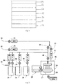
- Fig.1 is a schematic diagram of a structure of a non-polar blue light LED epitaxial wafer based on an LAO substrate of the present invention.
- the non-polar blue light LED epitaxial wafer based on the LAO substrate provided by the present invention includes a substrate.
- the substrate is the LAO substrate, and a buffer layer, a first non-doped layer, a first doped layer, a quantum well layer, an electron barrier layer and a second doped layer are arranged on the LAO substrate in sequence.
- the LAO substrate is also called a lanthanum aluminum oxide substrate which is composed of La, A1 and O elements, and the molecular formula is LaAlxOy.
- the non-polar blue light LED epitaxial wafer includes an LAO substrate 10, a non-polar m face GaN buffer layer 11, a non-polar non-doped u-GaN layer 12, a non-polar n-type doped GaN film 13, a non-polar InGaN/GaN quantum well layer 14, a non-polar m face AlGaN electron barrier layer 15 and a non-polar p-type doped GaN film 16, which are arranged from bottom to top in sequence.
- Fig.2 is a schematic diagram of a structure of a preparation device for a non-polar blue light LED epitaxial wafer based on an LAO substrate of the present invention.
- Fig.2 20 and 21 respectively represent NH3 and SiH4, which are used for providing N and Si; 22 represents H2, which is used as a carrier gas and for conveying Cp2Mg, TMGa and TMIn; 23, 24 and 25 respectively represent the Cp2Mg, the TMGa and the TMIn, which are used for providing Mg, Ga and In necessary for the growth of LED; 26 represents is a mechanical arm, which is used for conveying the substrate and a sample; 27 represents a radio frequency induction heater, which is used for heating and controlling the temperature of the substrate; 28 represents a graphite plate, which is used for bearing the LAO substrate; 29 represents a reaction chamber, which is used for generating chemical reactions on various reactant gases to generate the LED; 30 represents a spray head, which is a device used for uniformly jetting the fully mixed reactant gases onto the surface of the substrate; 31 represents a radio frequency plasma source device, which is used for providing active N; and 32-40 represent valves, which are used for controlling the gas conveyance states
- Fig.3 is a schematic flow chart of a preparation of a non-polar blue light LED epitaxial wafer based an LAO substrate of the present invention.
- the preparation method of the non-polar blue light LED epitaxial wafer grown on the LAO substrate of the present invention specifically includes the following steps:
- Fig.4 is an XRD test diagram of a non-polar blue light LED epitaxial wafer grown on a (001) face of an LAO substrate of the present invention.
- Fig.4 shows a full width at half maximum (FWHM) value of a X ray rocking curve of the LED epitaxial wafer as tested in the present invention.
- the full width at half maximum (FWHM) value is less than 0.1 degree, which indicates that the non-polar blue light LED epitaxial wafer prepared in the present invention has very good performance no matter on defect density or on crystalline quality.
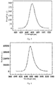
- Fig.5 is a PL spectrum test diagram of a non-polar m face blue light LED epitaxial wafer grown on an LAO substrate of the present invention at the room temperature.
- Fig.5 shows a emission peak having a wavelength of 460nm, and the full width at half maximum of 23nm, as tested by a PL spectrum at a temperature of 293K in the present invention. This indicates that the non-polar GaN film prepared in the present invention has very good performance on optical properties.
- Fig.6 is an EL spectrum test diagram of a non-polar m face blue light LED epitaxial wafer grown on an LAO substrate of the present invention at the room temperature.
- Fig.6 shows a emission peak having a wavelength of 461nm, the full width at half maximum of 22nm and the output power of 7.8mw@20mA, as tested by an EL spectrum at the temperature of 293K in the present invention. This indicates that the non-polar GaN film prepared in the present invention has very good performance on electrical properties.
- the present invention provides a non-polar blue light LED epitaxial wafer based on the LAO substrate and the preparation method thereof.
- the LAO substrate is adopted, and the non-polar m face GaN buffer layer, the non-polar non-doped u-GaN layer, the non-polar n-type doped GaN film, the non-polar InGaN/GaN quantum well, the non-polar m face AlGaN electron barrier layer and the non-polar p-type doped GaN film are arranged on the LAO substrate in sequence.
- the present invention has the advantages of simple growth process and low preparation cost
- the non-polar blue light LED epitaxial wafer prepared has the advantages of low defect density, good crystalline quality and good electrical and optical performances.
Landscapes
- Chemical & Material Sciences (AREA)
- Crystallography & Structural Chemistry (AREA)
- Engineering & Computer Science (AREA)
- Materials Engineering (AREA)
- Metallurgy (AREA)
- Organic Chemistry (AREA)
- Chemical Kinetics & Catalysis (AREA)
- General Chemical & Material Sciences (AREA)
- Inorganic Chemistry (AREA)
- Led Devices (AREA)
- Chemical Vapour Deposition (AREA)
Description
- The present invention relates to an LED epitaxial wafer and a preparation method thereof, and in particular, to a non-polar blue light LED epitaxial wafer based on an LAO substrate and a preparation method thereof.
- At present, substrates of LED blue light epitaxial wafers are mainly sapphire. The LED technology based on a sapphire substrate has two serious problems. Firstly, the mismatch rate of the sapphire and a GaN crystal lattice is as high as 17%. Such high lattice mismatch results in a high defect density of the sapphire based LED epitaxial wafer, thereby greatly influencing the luminous efficiency of an LED chip. Secondly, the price of the sapphire substrate is very high, resulting in very high production cost of a nitride LED.
- Another major reason for the low luminous efficiency of the LED chip is that the current GaN based LEDs in wide use have polarity. At present, the most ideal material for manufacturing of a high efficient LED device is GaN. The GaN is of a closely packed hexagonal crystal structure, whose crystal faces are divided into a polar face, which is a c face [(0001) face] and non-polar faces, which include an a face [(11-20) face] and an m face [(1-100) face]. Currently, most GaN based LEDs are constructed based on the polar face of the GaN. On the polar face of the GaN, the centroid of the Ga atom cluster does not coincide with the centroid of the N atom cluster, thus forming an electric dipole and generating a spontaneous polarization field and a piezoelectric polarization field, and further, causing a Quantum-confined Stark effect (QCSE). The QCSE causes electrons being separated from holes, and reduces the radiation recombination efficiency of charge carriers, which in turn influences the luminous efficiency of LED, and causes instability of a light emitting wavelength of the LED.
-
EP 1562237 A2 relates to Nitride-based semiconductor light emitting device and its method of manufacturing.CN 103268911 A relates to p-NiO/n-ZnO heterojunction light-emitting device and its preparation method.CN 203760505 U relates to apparatus for non-polar blue light LED epitaxial wafers for LAO substrates.US 2013/0240876 A1 relates to a method of growing a non-polar plane epitaxy layer of wurtzite structure.WO 2010/020077 A1 relates to a method of fabricating InGaAlN light-emitting device on a combined substrate.CN 103296159 A discloses InGaN/GaN multiple quantum well growing on La0.3Sr1.7AlTaO6 substrate and manufacturing method of InGaN/GaN multiple quantum well.US 2009/0008648 A1 discloses a GaN-based semiconductor element which can suppress a leakage current generated during reverse bias application. - The technical problem to be solved by the present invention is to provide a non-polar blue light LED epitaxial wafer based on an LAO substrate and a preparation method thereof. The non-polar blue light LED epitaxial wafer has the advantages of low defect density, good crystalline quality and good luminous performance, and having low preparation cost.
- The technical solution used for solving the above technical problem of the present invention is to provide a non-polar blue light LED epitaxial wafer based on an LAO substrate, including the substrate. The substrate is the LAO substrate, and a buffer layer, a first non-doped layer, a first doped layer, a quantum well layer, an electron barrier layer and a second doped layer are sequentially arranged on the LAO substrate.
- According to the non-polar blue light LED epitaxial wafer based on the LAO substrate, the buffer layer is a non-polar m face GaN buffer layer, the first non-doped layer is a non-polar non-doped u-GaN layer, the first doped layer is a non-polar n-type doped GaN film, the quantum well layer is a non-polar InGaN/GaN quantum well layer, the electron barrier layer is a non-polar m face AlGaN electron barrier layer, and the second doped layer is a non-polar p-type doped GaN film.
- To solve the above technical problem, the present invention provides a preparation method of a non-polar blue light LED epitaxial wafer based on an LAO substrate, including the following steps: a) adopting the LAO substrate, selecting the crystal orientation, and cleaning the surface of the LAO substrate; b) annealing the LAO substrate, and forming an AlN seed crystal layer on the surface of the LAO substrate; and c) sequentially forming a non-polar m face GaN buffer layer, a non-polar non-doped u-GaN layer, a non-polar n-type doped GaN film, a non-polar InGaN/GaN quantum well, a non-polar m face AlGaN electron barrier layer and a non-polar p-type doped GaN film on the LAO substrate by adopting metal organic chemical vapor deposition.
- According to the above preparation method of the non-polar blue light LED epitaxial wafer based on the LAO substrate, wherein the step b) includes the following processes: baking the LAO substrate at high temperature of 900-1200°C for 1-4 h followed by cooling to the room temperature in air, then passing N2 plasma to keep the temperature for 30-80 minutes, and forming the AlN seed crystal layer on the surface of the LAO substrate by radio frequency plasma enhanced metal organic chemical vapor deposition, wherein the flow of the N plasma is 40-90 sccm, and the radio frequency power for generating the plasma nitrogen is 200-500W.
- According to the above preparation method of the non-polar blue light LED epitaxial wafer based on the LAO substrate, wherein in the step c), the process of forming the non-polar m face GaN buffer layer may be as follows: cooling the LAO substrate to 400-800°C, passing TMGa and the N plasma, and controlling the pressure of a reaction chamber within the range of 53329 - 93326 Pa, the flow of the N plasma within the range of 40-90 sccm, the radio frequency power of generating the plasma nitrogen within the range of 200-700W, and the V/III ratio within the range of 800-1200.
- According to the above preparation method of the non-polar blue light LED epitaxial wafer based on the LAO substrate, wherein in the step c), the process of forming the non-polar non-doped u-GaN layer may be as follows: controlling the temperature of the LAO substrate with the range of 1000-1500°C, passing the TMGa, controlling the pressure of the reaction chamber at 53329 Pa and the V/III ratio at 180.
- According to the above preparation method of the non-polar blue light LED epitaxial wafer based on the LAO substrate, wherein in the step c), the process of forming the non-polar n-type doped GaN film may be as follows: controlling the temperature of the LAO substrate within the range of 1000-1300°C, passing the TMGa and SiH4, maintaining the flow of the SiH4 within the range of 60-100 sccm, and controlling the pressure of the reaction chamber at 31997 Pa, the V/III ratio at 160, and the dopped electron concentration within the range of 1.0×10¹⁷ to 5.3×1019cm-3.
- According to the above preparation method of the non-polar blue light LED epitaxial wafer based on the LAO substrate, wherein in the step c), the process of forming the non-polar InGaN/GaN quantum well may be as follows:
- forming a barrier layer: controlling the temperature of the LAO substrate within the range of 750-950°C, closing H2, passing the TEGa and ammonia gas, and controlling the pressure of the reaction chamber at 26664 Pa, the V/III ratio at 986, and the thickness within the range of 10-15nm; and
- forming a well layer: controlling the temperature of the LAO substrate within the range of 750-950°C, closing H2, passing the TEGa, TMIn and the ammonia gas, and controlling the pressure of the reaction chamber at 26664 Pa, the V/III ratio at 1439, and the thickness within the range of 2-4nm.
- According to the above preparation method of the non-polar blue light LED epitaxial wafer based on the LAO substrate, wherein in the step c), the process of forming the non-polar m face AlGaN electron barrier layer may be as follows: rising the temperature of the LAO substrate to 900-1050°C, passing the TMGa and the ammonia gas, and controlling the pressure of the reaction chamber at 26664 Pa and the V/III ratio at 986.
- According to the above preparation method of the non-polar blue light LED epitaxial wafer based on the LAO substrate, wherein in the step c), the process of forming the non-polar p-type doped GaN film may be as follows: controlling the temperature of the LAO substrate within the range of 900-1100°C, passing the TMGa, CP2Mg and the ammonia gas, maintaining the flow of the CP2Mg at 250-450 sccm, and controlling the pressure of the reaction chamber at 26664 Pa, the V/III ratio within the range of 1000-1250, and the hole doping concentration within the range of 1.0×10¹⁶ to 2.2×1018cm-3.
- Compared with the prior art, the present invention has the following beneficial effects that: according to the non-polar blue light LED epitaxial wafer based on the LAO substrate and the preparation method thereof provided by the present invention, the LAO substrate is adopted, and the buffer layer, the first non-doped layer, the first doped layer, the quantum well layer, the electron barrier layer and the second doped layer are arranged on the LAO substrate in sequence, so that the non-polar blue light LED epitaxial wafer has the advantages of low defect density, good crystalline quality and good luminous performance, and have low preparation cost.
-
-
Fig.1 is a schematic diagram of a structure of a non-polar blue light LED epitaxial wafer based on an LAO substrate of the present invention; -
Fig.2 is a schematic diagram of a structure of a preparation device for a non-polar blue light LED epitaxial wafer based on an LAO substrate of the present invention; -
Fig.3 is a schematic flow chart of a preparation of a non-polar blue light LED epitaxial wafer based an LAO substrate of the present invention; -
Fig.4 is an XRD test diagram of a non-polar blue light LED epitaxial wafer grown on a (001) face of an LAO substrate of the present invention; -
Fig.5 is a PL spectrum test diagram of a non-polar m face blue light LED epitaxial wafer grown on an LAO substrate of the present invention at the room temperature; -
Fig.6 is an EL spectrum test diagram of a non-polar m face blue light LED epitaxial wafer grown on an LAO substrate of the present invention at the room temperature. - The present invention will be further described below in combination with accompany drawings and embodiments.
-
Fig.1 is a schematic diagram of a structure of a non-polar blue light LED epitaxial wafer based on an LAO substrate of the present invention. - Please refer to
Fig.1 . The non-polar blue light LED epitaxial wafer based on the LAO substrate provided by the present invention includes a substrate. The substrate is the LAO substrate, and a buffer layer, a first non-doped layer, a first doped layer, a quantum well layer, an electron barrier layer and a second doped layer are arranged on the LAO substrate in sequence. According to the non-polar blue light LED epitaxial wafer grown on the LAO substrate provided by the present invention, the LAO substrate is also called a lanthanum aluminum oxide substrate which is composed of La, A1 and O elements, and the molecular formula is LaAlxOy. As shown inFig.1 , the non-polar blue light LED epitaxial wafer provided by the present invention includes anLAO substrate 10, a non-polar m faceGaN buffer layer 11, a non-polar non-doped u-GaNlayer 12, a non-polar n-type dopedGaN film 13, a non-polar InGaN/GaNquantum well layer 14, a non-polar m face AlGaNelectron barrier layer 15 and a non-polar p-type dopedGaN film 16, which are arranged from bottom to top in sequence. -
Fig.2 is a schematic diagram of a structure of a preparation device for a non-polar blue light LED epitaxial wafer based on an LAO substrate of the present invention. - Please refer to
Fig.2 . 20 and 21 respectively represent NH3 and SiH4, which are used for providing N and Si; 22 represents H2, which is used as a carrier gas and for conveying Cp2Mg, TMGa and TMIn; 23, 24 and 25 respectively represent the Cp2Mg, the TMGa and the TMIn, which are used for providing Mg, Ga and In necessary for the growth of LED; 26 represents is a mechanical arm, which is used for conveying the substrate and a sample; 27 represents a radio frequency induction heater, which is used for heating and controlling the temperature of the substrate; 28 represents a graphite plate, which is used for bearing the LAO substrate; 29 represents a reaction chamber, which is used for generating chemical reactions on various reactant gases to generate the LED; 30 represents a spray head, which is a device used for uniformly jetting the fully mixed reactant gases onto the surface of the substrate; 31 represents a radio frequency plasma source device, which is used for providing active N; and 32-40 represent valves, which are used for controlling the gas conveyance states of various pipelines. MFC represents a flow controller, which is used for controlling the gas flow to meet the growth demands. -
Fig.3 is a schematic flow chart of a preparation of a non-polar blue light LED epitaxial wafer based an LAO substrate of the present invention. - Please refer to
Fig.3 . the preparation method of the non-polar blue light LED epitaxial wafer grown on the LAO substrate of the present invention specifically includes the following steps: - step S 1: adopting the LAO substrate, selecting the crystal orientation, and cleaning the surface of the LAO substrate;
- step S2: annealing the LAO substrate, and forming an AlN seed crystal layer on the surface of the LAO substrate; and
- step S3: sequentially forming a non-polar m face GaN buffer layer, a non-polar non-doped u-GaN layer, a non-polar n-type doped GaN film, a non-polar InGaN/GaN quantum well, a non-polar m face AlGaN electron barrier layer and a non-polar p-type doped GaN film on the LAO substrate by metal organic chemical vapor deposition.
- A specific embodiment is provided below with the preparation steps and process conditions as follows:
- (1) adopting an LAO substrate, and selecting the crystal orientation;
- (2) cleaning the surface of the substrate;
- (3) annealing the substrate: baking the substrate at high temperature of 900-1200 °C for 1-4 h followed by cooling the substrate to the room temperature in air, then passing N2 plasma to keep the temperature for 30-80 minutes, and forming an AlN seed crystal layer on the surface of the substrate to provide a template for the growth of a GaN film, wherein the flow of the N plasma is 40-90 sccm, and the radio frequency power for generating the plasma nitrogen is 200-500W;
- (4) growing a non-polar m face GaN buffer layer by radio frequency (RF) plasma enhanced metal organic chemical vapor deposition (MOCVD), wherein the process conditions are as follows: the substrate is cooled to 400-800°C, the TMGa and the N plasma are passed, the pressure of a reaction chamber is 53329 - 93326 Pa, the flow of the N plasma is 40-90 sccm, the radio frequency power of generating the plasma nitrogen is 200-700W, and the V/III ratio is 800-1200;
- (5) growing a non-polar non-doped u-GaN layer by the MOCVD process, wherein the process conditions are as follows: the temperature of the substrate is 1000-1500°C, the TMGa is passed, the pressure of the reaction chamber is 53329 Pa, and the V/III ratio is 180;
- (6) growing a non-polar n-type doped GaN film by the MOCVD process, wherein the process conditions are as follows: the temperature of the substrate is 1000-1300°C, the TMGa and SiH4 are passed, the flow of the SiH4 is maintained at 60-100 sccm, the pressure of the reaction chamber is 26664 Pa, the V/III ratio is 160, and the doped electron concentration is 1.0×10¹⁷ to 5.3×1019cm-3;
- (7) growing a non-polar InGaN/GaN quantum well by the MOCVD process, wherein the process conditions for forming a barrier layer are as follows: , the temperature of the LAO substrate is 750-950 °C, H2 is closed, the TEGa and ammonia gas are passed, the pressure of the reaction chamber is 26664 Pa, the V/III ratio is 986, and the thickness is 10-15nm; and wherein the process conditions for forming a well layer are as follows: the temperature of the LAO substrate is 750-950 °C, H2 is closed, the TEGa, TMIn and the ammonia gas are passed, the pressure of the reaction chamber is 26664 Pa, the V/III ratio is 1439, and the thickness is 2-4nm;
- (8) growing a non-polar m face AlGaN electron barrier layer by the MOCVD process, wherein the process conditions are as follows: the temperature of the LAO substrate is raised to 900-1050°C, the TMGa and the ammonia gas are passed, the pressure of the reaction chamber is 26664 Pa, and the V/III ratio is 986; and
- (9) growing a non-polar p-type doped GaN film by the MOCVD process, wherein the process conditions are as follows: the temperature of the LAO substrate is 900-1100°C, the TMGa, CP2Mg and the ammonia gas are passed, the flow of the CP2Mg is maintained at 250-450 sccm, the pressure of the reaction chamber is 26664 Pa, the V/III ratio is 1000-1250, and the doped hole concentration is 1.0×10¹⁶ to 2.2×1018cm-3.
-
Fig.4 is an XRD test diagram of a non-polar blue light LED epitaxial wafer grown on a (001) face of an LAO substrate of the present invention. -
Fig.4 shows a full width at half maximum (FWHM) value of a X ray rocking curve of the LED epitaxial wafer as tested in the present invention. The full width at half maximum (FWHM) value is less than 0.1 degree, which indicates that the non-polar blue light LED epitaxial wafer prepared in the present invention has very good performance no matter on defect density or on crystalline quality. -
Fig.5 is a PL spectrum test diagram of a non-polar m face blue light LED epitaxial wafer grown on an LAO substrate of the present invention at the room temperature.Fig.5 shows a emission peak having a wavelength of 460nm, and the full width at half maximum of 23nm, as tested by a PL spectrum at a temperature of 293K in the present invention. This indicates that the non-polar GaN film prepared in the present invention has very good performance on optical properties. -
Fig.6 is an EL spectrum test diagram of a non-polar m face blue light LED epitaxial wafer grown on an LAO substrate of the present invention at the room temperature. -
Fig.6 shows a emission peak having a wavelength of 461nm, the full width at half maximum of 22nm and the output power of 7.8mw@20mA, as tested by an EL spectrum at the temperature of 293K in the present invention. This indicates that the non-polar GaN film prepared in the present invention has very good performance on electrical properties. - In summary, the present invention provides a non-polar blue light LED epitaxial wafer based on the LAO substrate and the preparation method thereof. The LAO substrate is adopted, and the non-polar m face GaN buffer layer, the non-polar non-doped u-GaN layer, the non-polar n-type doped GaN film, the non-polar InGaN/GaN quantum well, the non-polar m face AlGaN electron barrier layer and the non-polar p-type doped GaN film are arranged on the LAO substrate in sequence. Compared with the prior art, the present invention has the advantages of simple growth process and low preparation cost, and the non-polar blue light LED epitaxial wafer prepared has the advantages of low defect density, good crystalline quality and good electrical and optical performances.
Claims (7)
- A preparation method of a non-polar blue light LED epitaxial wafer based on a LAO substrate, the wafer having a LAO substrate (10), and a non-polar m face GaN buffer layer (11), a first non-polar non-doped u-GaN layer (12), a first non-polar n-type doped GaN film layer (13), a non-polar InGaN/GaN quantum well layer (14), a non-polar m face AlGaN electron barrier layer (15) and a second non-polar p-type doped GaN film layer (16) being sequentially arranged on the LAO substrate (10), wherein the method comprises the following steps:a) adopting the LAO substrate (10), selecting the crystal orientation, and cleaning the surface of the LAO substrate (10);b) annealing the LAO substrate (10), and forming an AlN seed crystal layer on the surface of the LAO substrate (10); andc) sequentially forming the non-polar m face GaN buffer layer (11), the first non-polar non-doped u-GaN layer (12), the first non-polar n-type doped GaN film (13), the non-polar InGaN/GaN quantum well layer (14), the non-polar m face AlGaN electron barrier layer (15) and the second non-polar p-type doped GaN film layer (16) on the LAO substrate (10) by adopting metal organic chemical vapor deposition; characterised in that said step b) comprises the following process:baking the LAO substrate (10) at high temperature of 900-1200 °C for 1-4 h followed by cooling to the room temperature in air, then passing N2 plasma to keep the temperature for 30-80 minutes, and forming the AlN seed crystal layer on the surface of the LAO substrate (10) by radio frequency plasma enhanced metal organic chemical vapor deposition, the flow of the N plasma is 40-90 sccm, and the radio frequency power for generating the plasma nitrogen is 200-500W.
- The preparation method of the non-polar blue light LED epitaxial wafer based on the LAO substrate according to claim 1, wherein in said step c), the process of forming the non-polar m face GaN buffer layer (11) is as follows: cooling the LAO substrate (10) to 400-800 °C, passing TMGa and the N plasma, and controlling the pressure of a reaction chamber within the range of 53329 - 93326 Pa, the flow of the N plasma within the range of 40-90 sccm, the radio frequency power of generating the plasma nitrogen within the range of 200-700W, and the V/III ratio within the range of 800-1200.
- The preparation method of the non-polar blue light LED epitaxial wafer based on the LAO substrate according to claim 1, wherein in said step c), the process of forming the non-polar non-doped u-GaN layer (12) is as follows: controlling the temperature of the LAO substrate (10) with the range of 1000-1500 °C, passing the TMGa, controlling the pressure of the reaction chamber at 53329 Pa and the V/III ratio at 180.
- The preparation method of the non-polar blue light LED epitaxial wafer based on the LAO substrate according to claim 1, wherein in said step c), the process of forming the non-polar n-type doped GaN film layer (13) is as follows: controlling the temperature of the LAO substrate (10) within the range of 1000-1300 °C, passing the TMGa and SiH4, maintaining the flow of the SiH4 within the range of 60-100 sccm, and controlling the pressure of the reaction chamber at 31997 Pa, the V/III ratio at 160, and the dopped electron concentration within the range of 1.0×10¹⁷ to 5.3×1019cm-3.
- The preparation method of the non-polar blue light LED epitaxial wafer based on the LAO substrate according to claim 1, wherein in said step c), the process of forming the non-polar InGaN/GaN quantum well layer (14) includes:forming a barrier layer: controlling the temperature of the LAO substrate (10) within the range of 750-950 °C, closing H2, passing the TEGa and ammonia gas, and controlling the pressure of the reaction chamber at 26664 Pa, the V/III ratio at 986, and the thickness within the range of 10-15nm; andforming a well layer: controlling the temperature of the LAO substrate (10) within the range of 750-950 °C, closing H2, passing the TEGa, TMIn and the ammonia gas, and controlling the pressure of the reaction chamber at 26664 Pa, the V/III ratio at 1439, and the thickness within the range of 2-4nm.
- The preparation method of the non-polar blue light LED epitaxial wafer based on the LAO substrate according to claim 1, wherein in said step c), the process of forming the non-polar m face AlGaN electron barrier layer (15) is as follows:rising the temperature of the LAO substrate (10) to 900-1050 °C, passing the TMGa and the ammonia gas, and controlling the pressure of the reaction chamber at 26664 Pa and the V/III ratio at 986.
- The preparation method of the non-polar blue light LED epitaxial wafer based on the LAO substrate according to claim 1, wherein in said step c), the process of forming the non-polar p-type doped GaN film layer (16) is as follows: controlling the temperature of the LAO substrate (10) within the range of 900-1100 °C, passing the TMGa, CP2Mg and the ammonia gas, maintaining the flow of the CP2Mg at 250-450 sccm, and controlling the pressure of the reaction chamber at 26664 Pa, the V/III ratio within the range of 1000-1250, and the hole doping concentration within the range of 1.0×10¹⁶ to 2.2×1018cm-3.
Priority Applications (1)
| Application Number | Priority Date | Filing Date | Title |
|---|---|---|---|
| PL15769396T PL3107128T3 (en) | 2014-03-24 | 2015-03-23 | Preparation method of a non-polar blue led epitaxial wafer based on lao substrate |
Applications Claiming Priority (2)
| Application Number | Priority Date | Filing Date | Title |
|---|---|---|---|
| CN201410112151.6A CN104600162B (en) | 2014-03-24 | 2014-03-24 | Preparation method of non-polar blue LED epitaxial wafer based on LAO substrate |
| PCT/CN2015/074828 WO2015144023A1 (en) | 2014-03-24 | 2015-03-23 | Non-polar blue led epitaxial wafer based on lao substrate and preparation method therefor |
Publications (3)
| Publication Number | Publication Date |
|---|---|
| EP3107128A4 EP3107128A4 (en) | 2016-12-21 |
| EP3107128A1 EP3107128A1 (en) | 2016-12-21 |
| EP3107128B1 true EP3107128B1 (en) | 2018-04-18 |
Family
ID=53125803
Family Applications (1)
| Application Number | Title | Priority Date | Filing Date |
|---|---|---|---|
| EP15769396.1A Active EP3107128B1 (en) | 2014-03-24 | 2015-03-23 | Preparation method of a non-polar blue led epitaxial wafer based on lao substrate |
Country Status (9)
| Country | Link |
|---|---|
| US (1) | US9978908B2 (en) |
| EP (1) | EP3107128B1 (en) |
| JP (1) | JP6326154B2 (en) |
| KR (1) | KR20160130411A (en) |
| CN (1) | CN104600162B (en) |
| CA (1) | CA2942999C (en) |
| PL (1) | PL3107128T3 (en) |
| RU (1) | RU2643176C1 (en) |
| WO (1) | WO2015144023A1 (en) |
Families Citing this family (12)
| Publication number | Priority date | Publication date | Assignee | Title |
|---|---|---|---|---|
| CN104600162B (en) | 2014-03-24 | 2016-01-27 | 上海卓霖半导体科技有限公司 | Preparation method of non-polar blue LED epitaxial wafer based on LAO substrate |
| CN106299041A (en) * | 2016-08-29 | 2017-01-04 | 华南理工大学 | The preparation method and application of the nonpolar LED being grown in r surface sapphire substrate |
| CN107170862B (en) * | 2017-06-08 | 2019-03-22 | 中国科学院半导体研究所 | A kind of non-polar plane light emitting diode with quantum dots and preparation method thereof |
| CN107887301B (en) * | 2017-09-27 | 2020-07-07 | 华灿光电(浙江)有限公司 | A kind of manufacturing method of light-emitting diode epitaxial wafer |
| CN108538972A (en) * | 2018-04-28 | 2018-09-14 | 华南理工大学 | Nonpolar ultraviolet LED and its preparation and application on a kind of graphical Si substrates |
| CN111276583A (en) * | 2020-02-12 | 2020-06-12 | 广东省半导体产业技术研究院 | GaN-based LED epitaxial structure, preparation method thereof and light emitting diode |
| CN113571607B (en) * | 2021-06-01 | 2022-08-12 | 华灿光电(浙江)有限公司 | Light-emitting diode epitaxial wafer with high luminous efficiency and its manufacturing method |
| CN114899258B (en) * | 2022-04-08 | 2024-03-12 | 华南理工大学 | Nonpolar AlGaN-based deep ultraviolet photodetector epitaxial structure and preparation method thereof |
| CN114875492B (en) * | 2022-04-18 | 2023-08-22 | 华南理工大学 | Nonpolar p-type GaN thin film epitaxial structure grown on LaAlO3 substrate and its preparation method |
| CN116885050B (en) * | 2023-06-01 | 2025-12-09 | 福建兆元光电有限公司 | Method for supplementing length of LED epitaxial wafer |
| CN116936700B (en) * | 2023-09-15 | 2023-12-22 | 江西兆驰半导体有限公司 | Light-emitting diode epitaxial wafer and preparation method thereof, light-emitting diode |
| CN117525232B (en) * | 2024-01-03 | 2024-03-29 | 江西兆驰半导体有限公司 | Light-emitting diode epitaxial wafer and preparation method thereof, light-emitting diode |
Family Cites Families (30)
| Publication number | Priority date | Publication date | Assignee | Title |
|---|---|---|---|---|
| JPH07201745A (en) * | 1993-12-28 | 1995-08-04 | Hitachi Cable Ltd | Semiconductor wafer and manufacturing method thereof |
| JP2002029896A (en) | 2000-07-05 | 2002-01-29 | National Institute Of Advanced Industrial & Technology | Crystal growth method for nitride semiconductor |
| US7112860B2 (en) * | 2003-03-03 | 2006-09-26 | Cree, Inc. | Integrated nitride-based acoustic wave devices and methods of fabricating integrated nitride-based acoustic wave devices |
| JP2005223165A (en) | 2004-02-06 | 2005-08-18 | Sanyo Electric Co Ltd | Nitride-based light emitting device |
| US7285799B2 (en) * | 2004-04-21 | 2007-10-23 | Philip Lumileds Lighting Company, Llc | Semiconductor light emitting devices including in-plane light emitting layers |
| TWI377602B (en) * | 2005-05-31 | 2012-11-21 | Japan Science & Tech Agency | Growth of planar non-polar {1-100} m-plane gallium nitride with metalorganic chemical vapor deposition (mocvd) |
| CN100399590C (en) * | 2005-06-15 | 2008-07-02 | 上海蓝光科技有限公司 | Method for growing epitaxial wafer with nitride light-emitting diode structure by MOCVD |
| CN100344006C (en) * | 2005-10-13 | 2007-10-17 | 南京大学 | Method for developing structure of LED device of InGaN/GaN quantum trap in M faces |
| JP4765751B2 (en) * | 2006-04-26 | 2011-09-07 | 三菱化学株式会社 | Method of manufacturing nitride semiconductor device |
| JP4770580B2 (en) * | 2006-05-15 | 2011-09-14 | 三菱化学株式会社 | Method of manufacturing nitride semiconductor device |
| TWM314427U (en) * | 2006-08-29 | 2007-06-21 | Sfi Electronics Technology Inc | LED assembly with having ESD protection capacity |
| WO2008073385A1 (en) * | 2006-12-11 | 2008-06-19 | The Regents Of The University Of California | Metalorganic chemical vapor deposition (mocvd) growth of high performance non-polar iii-nitride optical devices |
| JP4962130B2 (en) | 2007-04-04 | 2012-06-27 | 三菱化学株式会社 | GaN-based semiconductor light emitting diode manufacturing method |
| JP2009016467A (en) | 2007-07-03 | 2009-01-22 | Sony Corp | Gallium nitride semiconductor device, optical device using the same, and image display device using the same |
| JP2009283785A (en) | 2008-05-23 | 2009-12-03 | Showa Denko Kk | Group iii nitride semiconductor laminate structure and manufacturing method thereof |
| WO2010020077A1 (en) * | 2008-08-22 | 2010-02-25 | Lattice Power (Jiangxi) Corporation | Method for fabricating ingaain light-emitting device on a combined substrate |
| TWI425559B (en) | 2009-09-17 | 2014-02-01 | 國立交通大學 | Method for growing wurtzite structure semiconductor non-polar m-plane epitaxial layer by using single crystal oxide as substrate |
| CN101901761B (en) * | 2010-06-24 | 2011-10-19 | 西安电子科技大学 | MOCVD Growth Method of Nonpolar m-plane GaN on γ-plane LiAlO2 Substrate |
| TWI433231B (en) * | 2010-12-02 | 2014-04-01 | 晶元光電股份有限公司 | Method for manufacturing semiconductor component |
| US20120171797A1 (en) * | 2010-12-08 | 2012-07-05 | Applied Materials, Inc. | Seasoning of deposition chamber for dopant profile control in led film stacks |
| JP5558454B2 (en) | 2011-11-25 | 2014-07-23 | シャープ株式会社 | Nitride semiconductor light emitting device and method for manufacturing nitride semiconductor light emitting device |
| WO2013132812A1 (en) | 2012-03-05 | 2013-09-12 | パナソニック株式会社 | Nitride semiconductor light-emitting element, light source, and method for manufacturing same |
| TW201337050A (en) | 2012-03-14 | 2013-09-16 | 國立交通大學 | Non-polar crystal face of wurtzite structural material |
| CN203085627U (en) * | 2012-12-11 | 2013-07-24 | 华南理工大学 | Non-polar blue LED epitaxial wafer grown on LiGaO2 substrate |
| CN103268911B (en) | 2013-04-22 | 2016-05-18 | 浙江大学 | P-NiO/n-ZnO hetero-junctions luminescent device and preparation method thereof |
| CN103296159B (en) | 2013-05-31 | 2015-09-16 | 华南理工大学 | Grow the InGaN/GaN Multiple Quantum Well on strontium aluminate tantalum lanthanum substrate and preparation method |
| CN103311100A (en) * | 2013-06-14 | 2013-09-18 | 西安电子科技大学 | Production method of InN semiconductor component with nonpolar m plane GaN buffer layer |
| CN203760505U (en) | 2014-03-24 | 2014-08-06 | 上海卓霖信息科技有限公司 | Preparing apparatus for non-polar blue light LED epitaxial wafers for LAO substrates |
| CN104600162B (en) | 2014-03-24 | 2016-01-27 | 上海卓霖半导体科技有限公司 | Preparation method of non-polar blue LED epitaxial wafer based on LAO substrate |
| CN203850326U (en) * | 2014-03-24 | 2014-09-24 | 上海卓霖信息科技有限公司 | Nonpolar blue LED epitaxial wafer based on LAO substrate |
-
2014
- 2014-03-24 CN CN201410112151.6A patent/CN104600162B/en active Active
-
2015
- 2015-03-23 JP JP2016574326A patent/JP6326154B2/en active Active
- 2015-03-23 KR KR1020167026454A patent/KR20160130411A/en not_active Ceased
- 2015-03-23 WO PCT/CN2015/074828 patent/WO2015144023A1/en not_active Ceased
- 2015-03-23 PL PL15769396T patent/PL3107128T3/en unknown
- 2015-03-23 RU RU2016138668A patent/RU2643176C1/en active
- 2015-03-23 EP EP15769396.1A patent/EP3107128B1/en active Active
- 2015-03-23 US US15/128,639 patent/US9978908B2/en active Active
- 2015-03-23 CA CA2942999A patent/CA2942999C/en active Active
Non-Patent Citations (1)
| Title |
|---|
| None * |
Also Published As
| Publication number | Publication date |
|---|---|
| US9978908B2 (en) | 2018-05-22 |
| CA2942999C (en) | 2019-01-15 |
| JP6326154B2 (en) | 2018-05-16 |
| EP3107128A4 (en) | 2016-12-21 |
| KR20160130411A (en) | 2016-11-11 |
| PL3107128T3 (en) | 2018-09-28 |
| CA2942999A1 (en) | 2015-10-01 |
| CN104600162A (en) | 2015-05-06 |
| RU2643176C1 (en) | 2018-01-31 |
| JP2017513236A (en) | 2017-05-25 |
| EP3107128A1 (en) | 2016-12-21 |
| CN104600162B (en) | 2016-01-27 |
| WO2015144023A1 (en) | 2015-10-01 |
| US20170110627A1 (en) | 2017-04-20 |
Similar Documents
| Publication | Publication Date | Title |
|---|---|---|
| CA2942999C (en) | Non-polar blue led epitaxial wafer based on lao substrate and preparation method thereof | |
| CN101111945B (en) | Nitride semiconductor device and method of growing nitride semiconductor crystal layer | |
| CN109119515B (en) | A light-emitting diode epitaxial wafer and its manufacturing method | |
| CN103227251B (en) | A kind of growing method of GaN base light emitting diode epitaxial structure | |
| CN113410353B (en) | Light emitting diode epitaxial wafer and preparation method thereof | |
| CN106159052B (en) | Light emitting diode epitaxial wafer and manufacturing method thereof | |
| CN106098871A (en) | A kind of preparation method of light-emitting diode epitaxial wafer | |
| CN103811601A (en) | Method for GaN base LED multi-stage buffer layer growth with sapphire substrate serving as substrate | |
| CN108878609B (en) | ALN buffer layer of LED and its epitaxial growth method | |
| CN100403567C (en) | A method of avoiding or reducing V-type defects of blue-green light-emitting diode materials | |
| CN104576853A (en) | Epitaxial method for improving GaN based LED chip current spreading | |
| CN108598233A (en) | A kind of LED outer layer growths method | |
| CN110620168B (en) | LED epitaxial growth method | |
| CN107452841B (en) | LED epitaxial growth method based on graphene | |
| CN106409996A (en) | Epitaxial growth method capable of improving LED chip property uniformity | |
| CN109411573A (en) | A kind of LED epitaxial structure growing method | |
| CN104201257B (en) | Method for regulating and controlling LED epitaxial wafer wavelength uniformity through buffer layer | |
| CN106229397A (en) | A method for growing light-emitting diode epitaxial wafers | |
| CN203760505U (en) | Preparing apparatus for non-polar blue light LED epitaxial wafers for LAO substrates | |
| CN114464709A (en) | LED epitaxial wafer, epitaxial growth method and LED chip | |
| CN105679898A (en) | LED epitaxial structure with warpage adjusting structure layer and growth method thereof | |
| CN203850326U (en) | Nonpolar blue LED epitaxial wafer based on LAO substrate | |
| CN106299057A (en) | A kind of LED epitaxial structure improving brightness band 3D layer | |
| CN103325896A (en) | Gallium nitride-based LED (Light Emitting Diode) epitaxial growth method improving light emitting efficiency | |
| HK1230789B (en) | Preparation method of a non-polar blue led epitaxial wafer based on lao substrate |
Legal Events
| Date | Code | Title | Description |
|---|---|---|---|
| PUAI | Public reference made under article 153(3) epc to a published international application that has entered the european phase |
Free format text: ORIGINAL CODE: 0009012 |
|
| STAA | Information on the status of an ep patent application or granted ep patent |
Free format text: STATUS: REQUEST FOR EXAMINATION WAS MADE |
|
| 17P | Request for examination filed |
Effective date: 20160914 |
|
| A4 | Supplementary search report drawn up and despatched |
Effective date: 20161123 |
|
| AK | Designated contracting states |
Kind code of ref document: A1 Designated state(s): AL AT BE BG CH CY CZ DE DK EE ES FI FR GB GR HR HU IE IS IT LI LT LU LV MC MK MT NL NO PL PT RO RS SE SI SK SM TR |
|
| AX | Request for extension of the european patent |
Extension state: BA ME |
|
| RIN1 | Information on inventor provided before grant (corrected) |
Inventor name: LIU, ZHENGWEI Inventor name: GAO, HAI Inventor name: YIN, XIANGLIN Inventor name: CAI, ZHUORAN Inventor name: LIU, ZHI |
|
| STAA | Information on the status of an ep patent application or granted ep patent |
Free format text: STATUS: EXAMINATION IS IN PROGRESS |
|
| 17Q | First examination report despatched |
Effective date: 20170526 |
|
| DAV | Request for validation of the european patent (deleted) | ||
| DAX | Request for extension of the european patent (deleted) | ||
| REG | Reference to a national code |
Ref country code: HK Ref legal event code: DE Ref document number: 1230789 Country of ref document: HK |
|
| GRAP | Despatch of communication of intention to grant a patent |
Free format text: ORIGINAL CODE: EPIDOSNIGR1 |
|
| STAA | Information on the status of an ep patent application or granted ep patent |
Free format text: STATUS: GRANT OF PATENT IS INTENDED |
|
| RIC1 | Information provided on ipc code assigned before grant |
Ipc: H01L 21/02 20060101ALN20171128BHEP Ipc: C30B 29/40 20060101ALN20171128BHEP Ipc: C30B 25/18 20060101ALN20171128BHEP Ipc: H01L 33/02 20100101AFI20171128BHEP Ipc: H01L 33/16 20100101ALN20171128BHEP Ipc: H01L 33/12 20100101ALN20171128BHEP Ipc: H01L 33/00 20100101ALN20171128BHEP Ipc: H01L 33/32 20100101ALN20171128BHEP |
|
| INTG | Intention to grant announced |
Effective date: 20171213 |
|
| GRAS | Grant fee paid |
Free format text: ORIGINAL CODE: EPIDOSNIGR3 |
|
| GRAA | (expected) grant |
Free format text: ORIGINAL CODE: 0009210 |
|
| STAA | Information on the status of an ep patent application or granted ep patent |
Free format text: STATUS: THE PATENT HAS BEEN GRANTED |
|
| AK | Designated contracting states |
Kind code of ref document: B1 Designated state(s): AL AT BE BG CH CY CZ DE DK EE ES FI FR GB GR HR HU IE IS IT LI LT LU LV MC MK MT NL NO PL PT RO RS SE SI SK SM TR |
|
| REG | Reference to a national code |
Ref country code: GB Ref legal event code: FG4D |
|
| REG | Reference to a national code |
Ref country code: CH Ref legal event code: EP |
|
| REG | Reference to a national code |
Ref country code: DE Ref legal event code: R096 Ref document number: 602015010225 Country of ref document: DE |
|
| REG | Reference to a national code |
Ref country code: AT Ref legal event code: REF Ref document number: 991346 Country of ref document: AT Kind code of ref document: T Effective date: 20180515 |
|
| REG | Reference to a national code |
Ref country code: IE Ref legal event code: FG4D |
|
| REG | Reference to a national code |
Ref country code: NL Ref legal event code: MP Effective date: 20180418 |
|
| REG | Reference to a national code |
Ref country code: LT Ref legal event code: MG4D |
|
| REG | Reference to a national code |
Ref country code: HK Ref legal event code: GR Ref document number: 1230789 Country of ref document: HK |
|
| PG25 | Lapsed in a contracting state [announced via postgrant information from national office to epo] |
Ref country code: NL Free format text: LAPSE BECAUSE OF FAILURE TO SUBMIT A TRANSLATION OF THE DESCRIPTION OR TO PAY THE FEE WITHIN THE PRESCRIBED TIME-LIMIT Effective date: 20180418 |
|
| PG25 | Lapsed in a contracting state [announced via postgrant information from national office to epo] |
Ref country code: ES Free format text: LAPSE BECAUSE OF FAILURE TO SUBMIT A TRANSLATION OF THE DESCRIPTION OR TO PAY THE FEE WITHIN THE PRESCRIBED TIME-LIMIT Effective date: 20180418 Ref country code: LT Free format text: LAPSE BECAUSE OF FAILURE TO SUBMIT A TRANSLATION OF THE DESCRIPTION OR TO PAY THE FEE WITHIN THE PRESCRIBED TIME-LIMIT Effective date: 20180418 Ref country code: BG Free format text: LAPSE BECAUSE OF FAILURE TO SUBMIT A TRANSLATION OF THE DESCRIPTION OR TO PAY THE FEE WITHIN THE PRESCRIBED TIME-LIMIT Effective date: 20180718 Ref country code: FI Free format text: LAPSE BECAUSE OF FAILURE TO SUBMIT A TRANSLATION OF THE DESCRIPTION OR TO PAY THE FEE WITHIN THE PRESCRIBED TIME-LIMIT Effective date: 20180418 Ref country code: AL Free format text: LAPSE BECAUSE OF FAILURE TO SUBMIT A TRANSLATION OF THE DESCRIPTION OR TO PAY THE FEE WITHIN THE PRESCRIBED TIME-LIMIT Effective date: 20180418 Ref country code: SE Free format text: LAPSE BECAUSE OF FAILURE TO SUBMIT A TRANSLATION OF THE DESCRIPTION OR TO PAY THE FEE WITHIN THE PRESCRIBED TIME-LIMIT Effective date: 20180418 Ref country code: NO Free format text: LAPSE BECAUSE OF FAILURE TO SUBMIT A TRANSLATION OF THE DESCRIPTION OR TO PAY THE FEE WITHIN THE PRESCRIBED TIME-LIMIT Effective date: 20180718 |
|
| PG25 | Lapsed in a contracting state [announced via postgrant information from national office to epo] |
Ref country code: GR Free format text: LAPSE BECAUSE OF FAILURE TO SUBMIT A TRANSLATION OF THE DESCRIPTION OR TO PAY THE FEE WITHIN THE PRESCRIBED TIME-LIMIT Effective date: 20180719 Ref country code: LV Free format text: LAPSE BECAUSE OF FAILURE TO SUBMIT A TRANSLATION OF THE DESCRIPTION OR TO PAY THE FEE WITHIN THE PRESCRIBED TIME-LIMIT Effective date: 20180418 Ref country code: RS Free format text: LAPSE BECAUSE OF FAILURE TO SUBMIT A TRANSLATION OF THE DESCRIPTION OR TO PAY THE FEE WITHIN THE PRESCRIBED TIME-LIMIT Effective date: 20180418 Ref country code: HR Free format text: LAPSE BECAUSE OF FAILURE TO SUBMIT A TRANSLATION OF THE DESCRIPTION OR TO PAY THE FEE WITHIN THE PRESCRIBED TIME-LIMIT Effective date: 20180418 |
|
| REG | Reference to a national code |
Ref country code: AT Ref legal event code: MK05 Ref document number: 991346 Country of ref document: AT Kind code of ref document: T Effective date: 20180418 |
|
| PG25 | Lapsed in a contracting state [announced via postgrant information from national office to epo] |
Ref country code: PT Free format text: LAPSE BECAUSE OF FAILURE TO SUBMIT A TRANSLATION OF THE DESCRIPTION OR TO PAY THE FEE WITHIN THE PRESCRIBED TIME-LIMIT Effective date: 20180820 |
|
| REG | Reference to a national code |
Ref country code: DE Ref legal event code: R097 Ref document number: 602015010225 Country of ref document: DE |
|
| PG25 | Lapsed in a contracting state [announced via postgrant information from national office to epo] |
Ref country code: CZ Free format text: LAPSE BECAUSE OF FAILURE TO SUBMIT A TRANSLATION OF THE DESCRIPTION OR TO PAY THE FEE WITHIN THE PRESCRIBED TIME-LIMIT Effective date: 20180418 Ref country code: RO Free format text: LAPSE BECAUSE OF FAILURE TO SUBMIT A TRANSLATION OF THE DESCRIPTION OR TO PAY THE FEE WITHIN THE PRESCRIBED TIME-LIMIT Effective date: 20180418 Ref country code: SK Free format text: LAPSE BECAUSE OF FAILURE TO SUBMIT A TRANSLATION OF THE DESCRIPTION OR TO PAY THE FEE WITHIN THE PRESCRIBED TIME-LIMIT Effective date: 20180418 Ref country code: EE Free format text: LAPSE BECAUSE OF FAILURE TO SUBMIT A TRANSLATION OF THE DESCRIPTION OR TO PAY THE FEE WITHIN THE PRESCRIBED TIME-LIMIT Effective date: 20180418 Ref country code: DK Free format text: LAPSE BECAUSE OF FAILURE TO SUBMIT A TRANSLATION OF THE DESCRIPTION OR TO PAY THE FEE WITHIN THE PRESCRIBED TIME-LIMIT Effective date: 20180418 Ref country code: AT Free format text: LAPSE BECAUSE OF FAILURE TO SUBMIT A TRANSLATION OF THE DESCRIPTION OR TO PAY THE FEE WITHIN THE PRESCRIBED TIME-LIMIT Effective date: 20180418 |
|
| PLBE | No opposition filed within time limit |
Free format text: ORIGINAL CODE: 0009261 |
|
| STAA | Information on the status of an ep patent application or granted ep patent |
Free format text: STATUS: NO OPPOSITION FILED WITHIN TIME LIMIT |
|
| PG25 | Lapsed in a contracting state [announced via postgrant information from national office to epo] |
Ref country code: IT Free format text: LAPSE BECAUSE OF FAILURE TO SUBMIT A TRANSLATION OF THE DESCRIPTION OR TO PAY THE FEE WITHIN THE PRESCRIBED TIME-LIMIT Effective date: 20180418 Ref country code: SM Free format text: LAPSE BECAUSE OF FAILURE TO SUBMIT A TRANSLATION OF THE DESCRIPTION OR TO PAY THE FEE WITHIN THE PRESCRIBED TIME-LIMIT Effective date: 20180418 |
|
| 26N | No opposition filed |
Effective date: 20190121 |
|
| PG25 | Lapsed in a contracting state [announced via postgrant information from national office to epo] |
Ref country code: SI Free format text: LAPSE BECAUSE OF FAILURE TO SUBMIT A TRANSLATION OF THE DESCRIPTION OR TO PAY THE FEE WITHIN THE PRESCRIBED TIME-LIMIT Effective date: 20180418 |
|
| PG25 | Lapsed in a contracting state [announced via postgrant information from national office to epo] |
Ref country code: MC Free format text: LAPSE BECAUSE OF FAILURE TO SUBMIT A TRANSLATION OF THE DESCRIPTION OR TO PAY THE FEE WITHIN THE PRESCRIBED TIME-LIMIT Effective date: 20180418 |
|
| REG | Reference to a national code |
Ref country code: CH Ref legal event code: PL |
|
| PG25 | Lapsed in a contracting state [announced via postgrant information from national office to epo] |
Ref country code: LU Free format text: LAPSE BECAUSE OF NON-PAYMENT OF DUE FEES Effective date: 20190323 |
|
| REG | Reference to a national code |
Ref country code: BE Ref legal event code: MM Effective date: 20190331 |
|
| PG25 | Lapsed in a contracting state [announced via postgrant information from national office to epo] |
Ref country code: IE Free format text: LAPSE BECAUSE OF NON-PAYMENT OF DUE FEES Effective date: 20190323 Ref country code: LI Free format text: LAPSE BECAUSE OF NON-PAYMENT OF DUE FEES Effective date: 20190331 Ref country code: CH Free format text: LAPSE BECAUSE OF NON-PAYMENT OF DUE FEES Effective date: 20190331 |
|
| PG25 | Lapsed in a contracting state [announced via postgrant information from national office to epo] |
Ref country code: BE Free format text: LAPSE BECAUSE OF NON-PAYMENT OF DUE FEES Effective date: 20190331 |
|
| PG25 | Lapsed in a contracting state [announced via postgrant information from national office to epo] |
Ref country code: TR Free format text: LAPSE BECAUSE OF FAILURE TO SUBMIT A TRANSLATION OF THE DESCRIPTION OR TO PAY THE FEE WITHIN THE PRESCRIBED TIME-LIMIT Effective date: 20180418 |
|
| PG25 | Lapsed in a contracting state [announced via postgrant information from national office to epo] |
Ref country code: MT Free format text: LAPSE BECAUSE OF NON-PAYMENT OF DUE FEES Effective date: 20190323 |
|
| PG25 | Lapsed in a contracting state [announced via postgrant information from national office to epo] |
Ref country code: CY Free format text: LAPSE BECAUSE OF FAILURE TO SUBMIT A TRANSLATION OF THE DESCRIPTION OR TO PAY THE FEE WITHIN THE PRESCRIBED TIME-LIMIT Effective date: 20180418 |
|
| PG25 | Lapsed in a contracting state [announced via postgrant information from national office to epo] |
Ref country code: IS Free format text: LAPSE BECAUSE OF FAILURE TO SUBMIT A TRANSLATION OF THE DESCRIPTION OR TO PAY THE FEE WITHIN THE PRESCRIBED TIME-LIMIT Effective date: 20180818 |
|
| PG25 | Lapsed in a contracting state [announced via postgrant information from national office to epo] |
Ref country code: HU Free format text: LAPSE BECAUSE OF FAILURE TO SUBMIT A TRANSLATION OF THE DESCRIPTION OR TO PAY THE FEE WITHIN THE PRESCRIBED TIME-LIMIT; INVALID AB INITIO Effective date: 20150323 |
|
| PG25 | Lapsed in a contracting state [announced via postgrant information from national office to epo] |
Ref country code: MK Free format text: LAPSE BECAUSE OF FAILURE TO SUBMIT A TRANSLATION OF THE DESCRIPTION OR TO PAY THE FEE WITHIN THE PRESCRIBED TIME-LIMIT Effective date: 20180418 |
|
| REG | Reference to a national code |
Ref country code: DE Ref legal event code: R079 Ref document number: 602015010225 Country of ref document: DE Free format text: PREVIOUS MAIN CLASS: H01L0033020000 Ipc: H10H0020810000 |
|
| PGFP | Annual fee paid to national office [announced via postgrant information from national office to epo] |
Ref country code: GB Payment date: 20260323 Year of fee payment: 12 |
|
| PGFP | Annual fee paid to national office [announced via postgrant information from national office to epo] |
Ref country code: DE Payment date: 20260313 Year of fee payment: 12 |
|
| PGFP | Annual fee paid to national office [announced via postgrant information from national office to epo] |
Ref country code: FR Payment date: 20260330 Year of fee payment: 12 |
|
| PGFP | Annual fee paid to national office [announced via postgrant information from national office to epo] |
Ref country code: PL Payment date: 20260227 Year of fee payment: 12 |