EP3091702B1 - Verfahren und vorrichtung für direktumwandungsempfänger zur korrektur von gleichstrom-offset - Google Patents
Verfahren und vorrichtung für direktumwandungsempfänger zur korrektur von gleichstrom-offset Download PDFInfo
- Publication number
- EP3091702B1 EP3091702B1 EP15733140.6A EP15733140A EP3091702B1 EP 3091702 B1 EP3091702 B1 EP 3091702B1 EP 15733140 A EP15733140 A EP 15733140A EP 3091702 B1 EP3091702 B1 EP 3091702B1
- Authority
- EP
- European Patent Office
- Prior art keywords
- variable
- offset
- current control
- current
- control code
- Prior art date
- Legal status (The legal status is an assumption and is not a legal conclusion. Google has not performed a legal analysis and makes no representation as to the accuracy of the status listed.)
- Active
Links
Images



Classifications
-
- H—ELECTRICITY
- H04—ELECTRIC COMMUNICATION TECHNIQUE
- H04L—TRANSMISSION OF DIGITAL INFORMATION, e.g. TELEGRAPHIC COMMUNICATION
- H04L25/00—Baseband systems
- H04L25/02—Details ; arrangements for supplying electrical power along data transmission lines
- H04L25/06—DC level restoring means; Bias distortion correction ; Decision circuits providing symbol by symbol detection
-
- H—ELECTRICITY
- H04—ELECTRIC COMMUNICATION TECHNIQUE
- H04B—TRANSMISSION
- H04B1/00—Details of transmission systems, not covered by a single one of groups H04B3/00 - H04B13/00; Details of transmission systems not characterised by the medium used for transmission
- H04B1/06—Receivers
- H04B1/16—Circuits
- H04B1/30—Circuits for homodyne or synchrodyne receivers
-
- H—ELECTRICITY
- H03—ELECTRONIC CIRCUITRY
- H03D—DEMODULATION OR TRANSFERENCE OF MODULATION FROM ONE CARRIER TO ANOTHER
- H03D2200/00—Indexing scheme relating to details of demodulation or transference of modulation from one carrier to another covered by H03D
- H03D2200/0041—Functional aspects of demodulators
- H03D2200/0047—Offset of DC voltage or frequency
-
- H—ELECTRICITY
- H04—ELECTRIC COMMUNICATION TECHNIQUE
- H04B—TRANSMISSION
- H04B1/00—Details of transmission systems, not covered by a single one of groups H04B3/00 - H04B13/00; Details of transmission systems not characterised by the medium used for transmission
- H04B1/06—Receivers
- H04B1/16—Circuits
- H04B1/30—Circuits for homodyne or synchrodyne receivers
- H04B2001/305—Circuits for homodyne or synchrodyne receivers using DC offset compensation techniques
Definitions
- the present invention relates generally to a method and an apparatus for calibrating a direct current offset in a direct conversion receiver.
- a Radio Frequency (RF) receiver used in a wireless communication system can be divided into a receiver which uses a direct conversion method and a receiver which uses a heterodyne method.
- the direct conversion method indicates a method for directly converting a low frequency baseband signal and a high frequency signal, that is, an RF signal
- the heterodyne method indicates a method for going through an intermediate step which converts to an Intermediate Frequency (IF) and then converting and processing to an intended frequency band signal without directly converting a baseband signal and an RF signal.
- IF Intermediate Frequency
- the direct conversion method compared with the heterodyne method, does not require a part for performing the IF conversion and includes a plurality of gain stages at an analog baseband stage.
- a great Direct Current (DC) offset can generate in proportion to a gain.
- the DC offset increases, a performance of the receiver lowers. In a severe case, it can be difficult to receive a signal.
- the DC offset indicates a common mode voltage difference generated in two signal paths, that is, a DC level difference in a circuit of a differential structure having the two signal paths.
- the related art used a method for cutting off low frequencies using a high pass filter or a low pass filter.
- a method for cutting off low frequencies using a high pass filter or a low pass filter has a disadvantage of causing signal attenuation according to a modulation method or a cutoff frequency of the pass filter and thus degrading the performance of the receiver.
- US2007/230622 A1 discloses a method and apparatus for the correction of direct current offsets in radio output signals.
- US2013/223569 A1 discloses a wireless receiver including a control unit configured to correct a DC offset of a mixer by allowing a current to flow into an amplification circuit.
- US2002/197975 A1 discloses a method for measuring a difference in DC offsets associated with different gain settings in a direct conversion receiver having a variable gain.
- US2005/0075088 A1 discloses a receiving circuit of a direct conversion system that includes a DC offset cancellation operation.
- US2009/0212983 A1 an integrated circuit device and electronic instrument that includes a controller that calculates and sets offset adjustment data for amplifiers of the integrated circuit device.
- the present invention determines the current control code of the variable Digital to Analog Converters (DACs) so as to minimize the Direct Current (DC) offset per variable gain amplifiers in the direct conversion in receiver including the plurality of variable gain amplifiers and the plurality of variable DAC, and calibrates the DC offset based on the determined current control code.
- DACs Digital to Analog Converters
- DC Direct Current
- an expression such as “have”, “can have”, “include” or “can include” refers to presence such as a corresponding function, operation, or component of the disclosure, and does not limit additional one or more functions, operations, or components.
- a term such as “include” or “have” is intended to designate presence of a characteristic, a number, a step, an operation, a component, a part or their combination disclosed in the specification, and it should be appreciated that it does not exclude in advance the presence or addition of one or more other characteristics, numbers, steps, operations, components, parts, or combinations thereof.
- an expression such as “A or B” or “at least one of A or/and B” includes any and every combination of words listed together.
- “A or B” or “at least one of A or/and B” each may include A, B, or both of A and B.
- Expressions such as "1st”, “2nd", “first” or “second” used in various embodiments of the present invention can modify various components of various embodiments, but does not limit the corresponding components.
- the expressions do not limit to sequence and/or importance of the corresponding components.
- the expressions can be used to distinguish one component from another component.
- a first user device and a second user device both are user devices and represent different user devices.
- a first component can be named as a second component, and similarly, a second component can be named as a first component without departing from the scope of various embodiments of the present invention.
- An expression “configured to (or set)” used in the present document can be used interchangeably with, for example, “suitable for,” “having the capacity to,” “designed to,” “adapted to,” “made to,” or “capable of' according to a situation.
- a term “configured to (or set)” does not only mean “specifically designed to” by hardware. Instead, in some situations, an expression “apparatus configured to” can mean that the apparatus “can” operate together with another apparatus or components.
- a phrase "a processor configured (or set) to perform A, B, and C" can represent an exclusive processor (e.g., an embedded processor) for performing a corresponding operation, or a generic-purpose processor (e.g., a Central Processing Unit (CPU) or an application processor) which can perform a corresponding operation by executing one or more software programs stored in a memory device.
- an exclusive processor e.g., an embedded processor
- a generic-purpose processor e.g., a Central Processing Unit (CPU) or an application processor
- the present invention is to explain a method and an apparatus for canceling a Direct Current (DC) offset using a plurality of variable Digital Analog Converters (DACs) in a direct conversion receiver.
- DC Direct Current
- DACs variable Digital Analog Converters
- FIG. 1 shows a structure of a direct conversion receiver 100 according to an embodiment of the present invention.
- the direct conversion receiver 100 can include at least one antenna 101, a Variable Low Noise Amplifier (VLNA) 110, a mixer 120, a plurality of Variable Gain Amplifiers (VGAs) 130-0 through 130-n, a plurality of Variable Digital to Analog Converters (VDACs) 140-0 through 140-n, a DC offset cancellation unit 150, an Analog to Digital Converter (ADC) 160, and a DC offset monitoring unit 170.
- VLNA Variable Low Noise Amplifier
- VGAs Variable Gain Amplifiers
- VDACs Variable Digital to Analog Converters
- ADC Analog to Digital Converter
- the variable low noise amplifier 110 amplifies a high frequency Radio Frequency (RF) signal received from the antenna 101 and provides to the mixer 120.
- the variable low noise amplifier 110 can amplify the high frequency RF signal based on a gain value which is changed according to a preset scheme.
- the mixer 120 converts a signal received from the variable low noise amplifier 110 to a baseband signal and thus provides as an input of the zero-th variable gain amplifier 130-0 disposed at the very front end of the plurality of variable gain amplifiers 130-0 through 130-n.
- the mixer 120 can generate a baseband signal by mixing the signal received from the variable low noise amplifier110 and with a local oscillator signal, and output the generated baseband signal to the 0-th variable gain amplifier 130-0.
- Each of the plurality of variable gain amplifiers 130-0 through 130-n receive an output current from the corresponding variable DACs 140-0 through 140-n, and amplify and output an amplitude of the input signal based on a gain control signal according to an Automatic Gain Control (AGC) code.
- AGC Automatic Gain Control
- each of the plurality of variable gain amplifiers 130-0 through 130-n can be an amplifier of a differential structure having two input paths and two output signal paths.
- the zero-th variable gain amplifier 130-0 receives the baseband signal from the mixer 120, amplifies its amplitude according to the AGC code, and then provides the amplified signal to the first variable gain amplifier 130-1.
- the first variable gain amplifier 130-1 receives the signal output from the zero-th variable gain amplifier 130-0, amplifies the amplitude according to the AGC code, and then provides the amplified signal to the second variable gain amplifier 130-2.
- each of the plurality of variable gain amplifiers 130-0 through 130-n can amplify the baseband signal output from the mixer 120 multiple times, and the signal amplified multiple times is provided as an input of the ADC 160.
- Each of the plurality of variable DACs 140-0 through 140-n include a circuit and switches for generating a base current I B in the form of the power of two.
- Each of the plurality of variable DACs 140-0 through 140-n can change a current output to a corresponding variable gain amplifier by controlling on/off of the switch based on the current control code input from the DC offset cancellation unit 150.
- a DC offset of an output stage of a corresponding variable gain amplifier 130-0 through 130-n can be changed according to the output current of each of the variable DACs 140-0 through 140-n.
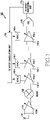
- each variable DAC 140 includes, as shown in FIG. 2 , a plurality of current sources 146-0 through 146-n for generating the base current as the power of two ( I B ,2 I B ,4 I B , ..., 2 n I B ,), and a plurality of switches 144-0 through 144-n connected to the current sources 146-0 through 146-n respectively, and can include a base current control circuit 142 for providing the base current to each of the current sources 146-0 through 146-n.
- the variable DAC 140 receives a base current control code from the DC current cancellation unit 150, and controls the base current provided to the plurality of current sources 146-0 through 146-n according to the input base current control code.
- the plurality of current sources 146-0 through 146-n each generate the current corresponding to the power of two of the base current while a corresponding switch 144-0 through 144-n is turned on.
- a magnitude of the current generated in each of the plurality of current sources 146-0 through 146-n can have a linear increasing form.
- the plurality of switches 144-0 through 144-n each are turned on or off according to the DAC current control code provided from the DC offset cancellation unit 150, and provides a current generated from the current source connected to a corresponding switch, to an output stage.
- the plurality of switches 144-0 through 144-n each may be turned on simultaneously or turned off simultaneously, and some switches may be turned off and the remaining switches may be turned on, according to the DAC current control code.
- the DC offset cancellation unit 150 performs a function for cancelling a DC offset generated by the variable gain amplifiers 130-0 through 130-n according to an embodiment of the present invention. Based on the DC offset of the output stage of the ADC 160 provided from the DC offset monitoring unit 170, the DC offset cancellation unit 150 retrieves and determines the DAC current control code which minimizes the DC offset per AGC code, and stores the determined DAC current control code information per AGC.
- the AGC code indicates a code for controlling the gain value of the plurality of variable gain amplifiers, and can be preset by a designer.
- the DC offset cancellation unit 150 controls, when the system is powered on, the gain of the plurality of variable gain amplifier 130-0 through 130-n per AGC code while the whole receive path of the receiver is turned on and retrieves the current control code of each variable DAC to minimize the DC offset monitored at the output stage of the ADC 160.
- the DC offset cancellation unit 150 controls the gain of the plurality of variable gain amplifiers 130-0 through 130-n based on the AGC code, and sequentially searches the DAC current control code with respect to each of the plurality of variable DACs 140-0 through 140-n.
- the DC offset cancellation unit 150 changes the current control code of the zero-th variable DAC 140-0 disposed at the very front end among the plurality of variable DACs 140-0 through 140-n, and retrieves the current control code of the zero-th DAC 140-0 to minimize the DC offset monitored at the output stage of the ADC.
- the current control code of the zero-th variable DAC 140-0 can be searched through a binary search method, and the current control codes of the other DACs 140-1 through 140-n should be maintained at a constant value during the current control code search of the zero-th variable DAC 140-0.
- the DC offset cancellation unit 150 changes the current control code of the first variable DAC 140-1 and searches for the current control code of the first variable DAC 140-1 to minimize the DC offset monitored at the output stage of the ADC.
- the current control code of the first variable DAC 140-1 can be searched through the binary search method, and the current control codes of the other DACs 140-0 and 140-2 through 14-n should be maintained at a constant value during the current control code search of the first variable DAC 140-1.
- the DC offset cancellation unit 150 determines the current control code for each of the plurality of variable DACs 140-0 through 140-n, and maps and stores the current control codes of the plurality of variable DACs 140-0 through 140-n, that is, a current control code set (or a current control code combination) with the first AGC code.
- the DC offset cancellation unit 150 when retrieving the current control code of each variable DAC to minimize the DC offset, the DC offset cancellation unit 150 outputs a base current control signal so that the variable DAC at the very front end among the plurality of variable DACs 140 uses the smallest base current and the variable DAC at a later end uses a greater base current than the front-end DAC.
- FIG. 4 it is to consider a situation where the DC offset increases in the variable gain amplifier at the later end among the plurality of variable gain amplifiers 130-0 through 130-n according to a feature that the DC offset increases as the gain increases. That is, it is to more precisely control the DC offset generated by the variable gain amplifier at the later end by controlling an output current range provided to the variable gain amplifier at the later end to be wider than an output current range provided to the variable gain amplifier at the front.
- the DC offset cancellation unit 150 obtains the DAC current control code set for all of the preset AGC codes in the above-stated manner, and maps and stores the obtained DAC current control code set with corresponding AGC codes.
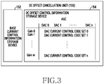
- the DC offset cancellation unit 150 includes, as shown in FIG. 3 , a base current control information storage device 152 and a DC offset control information storage device 154, and can store base current control information and DAC current control code information per AGC code.
- the base current control information storage device 152 can store the base current information to be provided to each of the variable DACs, and store the base current change information according to a temperature change.
- the DC offset control information storage device 154 can, as described above, represent a mapping relationship of the current control codes of the variable DACs for each AGC code by storing the DAC current control code set for the AGC codes respectively.
- the DC offset cancellation unit 150 minimizes the DC offset by controlling the output current of the variable DACs 140-0 through 140-n based on the DAC current control code set corresponding to the selected AGC code.
- the DC offset cancellation unit 150 can periodically monitor the DC offset monitored at the output stage of the ADC 160 during an operation using a preset DAC current control code set, and perform the DC offset calibration process using the base current control when the DC offset is outside a preset threshold range. For example, the DC offset cancellation unit 150 can periodically monitor the DC offset after the initial DC offset calibration process, and when the monitored DC offset is outside the threshold range, sequentially change the base current of each DAC so that the DC offset corresponds to the threshold range without changing the DAC current control code set. This is to prepare for a situation where a current amount of each variable DAC changes because a temperature of the system changes as the time passes and thus the DC offset can change.
- the ADC 160 converts and outputs the amplified analog signal from the n-th variable gain amplifier 130-n to a digital signal.
- the DC offset monitoring unit 170 monitors a DC offset value by monitoring the output signal of the ADC 160. For example, the DC offset monitoring unit 170 can monitor a voltage value output through the two output signal paths of the ADC 160, and determine a difference value of the two monitored voltage values as the DC offset. The DC offset monitoring unit 170 provides the monitored DC offset to the DC offset cancellation unit 150. When the system including the direct conversion receiver 100 is powered on, the DC offset monitoring unit 170 can estimate the DC offset for the DC offset calibration and perform an operation for providing the estimated DC offset value to the DC offset cancellation unit 150. Also, the DC offset monitoring unit 170 may periodically estimate the DC offset and provide it to the DC offset cancellation unit 150.
- an apparatus for DC offset calibration of a direct conversion receiver can include a plurality of variable gain amplifiers for amplifying an input signal based on a gain control value, a DC offset monitoring unit for monitoring a DC offset for an output signal of the plurality of variable gain amplifiers, a plurality of variable DACs for controlling a current applied to each of the plurality of variable gain amplifiers according to a current control code, and a DC offset cancellation unit for determining a current control code set which minimizes the DC offset value per preset gain control value.
- variable DAC can include a plurality of switches for being turned on/off according to the current control code, a plurality of current sources connected to the switches respectively and generating a current corresponding to a power of two, and a base current control circuit for providing a base current to the plurality of current sources.
- the DC offset cancellation unit when the direct conversion receiver is turned on, can obtain the current control code of each DAC to minimize the DC offset value by changing a current control code for each of the plurality of variable DACs, per preset gain control value.
- the DC offset cancellation unit can search for a current control code to minimize the DC offset value from a DAC disposed at a front end among the plurality of variable DACs, configure one current control code set with the current control code searched for the plurality of variable DACs respectively, and map and store the configured current control code set with the particular gain control value.
- the DC offset cancellation unit when searching for the current control code for each of the plurality of variable DACs, can control a base current of a variable DAC disposed at a back end to have a greater value than a base current of a variable DAC disposed at a front end among the plurality of variable DACs.
- the DC offset cancellation unit when searching for the current control code for each of the plurality of variable DACs, can search for the current control code using a binary search method.
- an Analog to Digital Converter for converting a signal output from the plurality of variable gain amplifiers to a digital signal is further included, and the DC offset monitoring unit can monitor a DC offset for an output signal of the ADC.
- ADC Analog to Digital Converter
- the DC offset cancellation unit in a signal reception mode, can control an output current of the variable DAC using the determined current control code set corresponding to a gain control value.
- the DC offset cancellation unit in a signal reception mode, can compare a DC offset value periodically provided from the DC offset monitoring unit with a preset threshold range, and when the DC offset value is outside the preset threshold range, regulate a base current used by the plurality of variable DACs.
- the DC offset cancellation unit when the DC offset value is outside the preset threshold range, can maintain a current control set being used by the plurality of variable DACs without changing.
- FIG. 5 depicts a DC offset calibration process in a direct conversion receiver 100 according to an embodiment of the present invention.
- FIG. 5 illustrates an initial DC offset calibration process which retrieves and stores a DCA current control code set for every AGC code preset when the system including the direct conversion receiver 100 is powered on.
- the direct conversion receiver 100 detects the power-on of the system in step 501. After detecting the system power on, the direct conversion receiver 100 sets the gain value of the plurality of variable gain amplifiers 130-0 through 130-n based on a preset i-th AGC code in step 503.
- the AGC code indicates a code for controlling the gain value of the plurality of variable gain amplifiers 130-0 through 130-n, and can be preset by the designer.
- the direct conversion receiver 100 determines the DAC current control code which minimizes the DC offset by controlling the output current of the j-th variable DAC in step 505. For example, while the gains of the plurality of variable gain amplifiers 130-0 through 130-n are set based on a first AGC code, the direct conversion receiver 100 can change the output current by controlling on/off of the current control switches 144-0 through 144-0 through the current control code change in the j-th variable DAC.
- the direct conversion receiver 100 can monitor the DC offset of the output stage of the ADC 160 per current control code of the j-th variable DAC, and thus determine the current control code which minimizes the DC offset.
- the direct conversion receiver 100 can retrieve and determine the current control code which minimizes the DC offset using the binary search method.
- the direct conversion receiver 100 maintains the current control code of the remaining variable DACs excluding the j-th variable DAC as a constant value so that the DC offset is not changed by other variable DACs during the DAC current control code search for the j-th variable DAC.
- the direct conversion receiver 100 checks whether the current control code is determined for each of m-ary DACs in step 507.
- m indicates the total number of variable DACs connected to the plurality of variable gain amplifiers in the direct conversion receiver 100. That is, with the gain of the plurality of variable gain amplifiers 130-0 through 130-n set based on the i-th AGC code, the direct conversion receiver 100 checks whether the current control code for every variable DAC is determined. When the current control code for every variable DAC is not determined, the direct conversion receiver 100 updates j with j+1 and increases the base current in step 509, and then proceeds to step 505.
- the direct conversion receiver 100 updates the value j so as to retrieve the DAC current control code for a next variable DAC. Also, the direct conversion receiver 100 regulates the magnitude of the base current so that the magnitude of the base current of the next variable DAC is greater than the magnitude of the base current of a front-end variable DAC.
- the direct conversion receiver 100 maps and stores the DAC current control code set determined for the m-ary DACs respectively with the i-th AGC code in step 511. That is, the direct conversion receiver 100 can map and store the DAC current control code set including the current control codes determined for the plurality of variable DACs respectively determined with the determined gain of the plurality of variable gain amplifiers 130-0 through 130-n, with the i-th AGC code. For example, as shown in FIG.
- the i-th AGC code indicating Gain 0 can be mapped and stored with a DAC current control code set which combines a current control code of DAC 0, a current control code of DAC 1, ..., and, a current control code of DAC n.
- the direct conversion receiver 100 checks whether the DAC current control code set is stored for all of the preset AGC codes in step 513. When the DAC current control code set is not stored for all of the preset AGC codes, the direct conversion receiver 100 updates i with i+1 in step 515 and proceeds to step 503. That is, when the DAC current control code set is not obtained for all of the preset AGC codes, the direct conversion receiver 100 updates the value i to search for the DAC current control code with respect to the AGC code not obtaining the DAC current control code set.
- the direct conversion receiver 100 finishes the DC offset calibration process according to an embodiment of the present invention.
- an embodiment of the present invention can prevent performance degradation of the direct conversion receiver 100 by minimizing the DC offset by controlling the output current of each DAC with the pre-stored DAC current control code set according to the AGC code when a signal is actually received.
- FIG. 6 depicts a DC offset calibration process in a direct conversion receiver 100 according to another embodiment of the present invention.
- FIG. 6 illustrates a periodic DC offset calibration process conducted after an initial DC offset calibration process is finished in a system including the direct conversion receiver 100.
- the direct conversion receiver 100 monitors a DC offset of the output stage of the ADC 160 in step 601. Next, the direct conversion receiver 100 determines whether the monitored DC offset is outside a preset threshold range in step 603
- the direct conversion receiver 100 determines that the DC offset calibration is not necessary, stands by for a certain time according to a preset cycle in step 607, and then goes back to step 601.
- the direct conversion receiver 100 determines that the DC offset calibration is necessary and controls the base current of each of the plurality of DAC 140-0 through 140-n in step 605. That is, when the monitored DC offset is outside the preset threshold range, the direct conversion receiver 100 can sequentially control the base current of each DAC so that the DC offset of the ADC output stage corresponds to the threshold range while not changing the DAC current control code which is currently set to each DAC. Next, the direct conversion receiver 100 returns to step 601 and performs the following steps.
- Operation according to an embodiment of the present invention can be implemented by a single controller.
- program instructions for fulfilling operations embodied by various computers can be recorded in a computer-readable medium.
- the computer-readable medium can include program instructions, data files, and data structures, alone or in combination.
- the program instructions may be specially designed and configured for the present invention or known to and used by those of ordinary skilled in the art.
- Examples of the computer-readable recording medium include a hard disk, a magnetic medium such as a floppy disk and a magnetic tape, an optical recording medium such as Compact Disc (CD)-Read Only Memory (ROM) or a Digital Versatile Disc (DVD), magnetooptical medium such as a floptical disk, and hardware devices specially configured to store and execute program instructions such as ROM, Random Access Memory (RAM), and flash memory.
- Examples of the program instructions include not only a machine code made by a compiler but also a high-level language code executable by a computer using an interpreter.
- the computer-readable recording medium storing the computer program is also included in the present invention. Accordingly, the scope of the present invention is not limited and confined to the described embodiments, but is defined by the appended claims.
Landscapes
- Engineering & Computer Science (AREA)
- Computer Networks & Wireless Communication (AREA)
- Signal Processing (AREA)
- Power Engineering (AREA)
- Circuits Of Receivers In General (AREA)
- Control Of Amplification And Gain Control (AREA)
Claims (11)
- Vorrichtung zur Offset-Kalibrierung von Gleichstrom, DC, eines Direktumwandlungsempfängers, die Vorrichtung umfassend:eine Vielzahl von in Reihe geschalteten Verstärkern variabler Verstärkung (VGA 0 - VGA n), die konfiguriert sind, um ein Eingangssignal basierend auf den jeweiligen voreingestellten Verstärkungssteuerwerten zu verstärken;eine DC-Offset-Überwachungseinheit (170), die konfiguriert ist, um ein DC-Offset für ein Ausgangssignal der Vielzahl von Verstärkern variabler Verstärkung (VGA 0 - VGA n) zu überwachen;eine Vielzahl von variabler Digital-Analog-Wandlern, DACs, (140-0 - 140-n), wobei jeder der Vielzahl von variablen DACs konfiguriert ist, um einen Strom, der an einen entsprechenden der Vielzahl von Verstärkern variabler Verstärkung (VGA 0 - VGA n) angelegt wird, gemäß einem jeweiligen Stromsteuercode zu steuern; undeine DC-Offset-Unterdrückungseinheit (150), die konfiguriert ist, um aus einer Vielzahl von Stromsteuercodes einen Stromsteuercodesatz zu bestimmen, der den DC-Offset-Wert für jeden der voreingestellten Verstärkungssteuerwerte minimiert,wobei, in einem Signalempfangsmodus, die DC-Offset-Unterdrückungseinheit (150) ferner zu Folgendem konfiguriert istSteuern der Ausgangsströme der Vielzahl von variablen DACs (140-0 - 140-n) unter Verwendung des Stromsteuercodesatzes, der den Verstärkungssteuerwerten entspricht,Vergleichen des von der DC-Offset-Überwachungseinheit (170) periodisch bereitgestellten DC-Offset-Werts mit einem voreingestellten Schwellenwertbereich, undwenn der DC-Offset-Wert außerhalb des voreingestellten Schwellenbereichs ist, Regulieren eines Basisstroms (IB), der von der Vielzahl von variablen DACs (140-0 - 140-n) verwendet wird, undBeibehalten des Stromsteuercodesatzes, der von der Vielzahl von variablen DACs (140-0 - 140-n) verwendet wird, ohne Änderung.
- Vorrichtung nach Anspruch 1, wobei jeder der Vielzahl von variablen DACs (140-0 - 140-n) Folgendes umfasst:eine Vielzahl von Schaltern (144-0 - 144-n), die konfiguriert sind, um entsprechend dem Stromsteuercode ein- und ausgeschaltet zu werden;eine Vielzahl von Stromquellen (146-0 - 146-n), die jeweils mit der Vielzahl von Schaltern (144-0 - 144-n) verbunden und konfiguriert sind, um einen Strom zu erzeugen, der einer Leistung von zwei Basisströmen (IB) entspricht, die der Vielzahl von Stromquellen zugeführt werden; undeine Basisstrom-Steuerschaltung (142) zum Bereitstellen des Basisstroms an die Vielzahl von Stromquellen (146-0 - 146-n).
- Vorrichtung nach Anspruch 1, wobei, wenn der Direktumwandlungsempfänger eingeschaltet ist, die DC-Offset-Unterdrückungseinheit (150) ferner konfiguriert ist, um einen Stromsteuercode für jeden der Vielzahl von variablen DACs (140-0 - 140-n) zu bestimmen, um den DC-Offset-Wert zu minimieren, indem sie den Stromsteuercode für jeden der Vielzahl von variablen DACs (140-0 - 140-n) pro voreingestelltem Verstärkungssteuerwert ändert.
- Vorrichtung nach Anspruch 3, wobei, wenn eine Verstärkung der Vielzahl von Verstärkern variabler Verstärkung (VGA 0 - VGA n) auf einen bestimmten Verstärkungssteuerwert eingestellt ist, die DC-Offset-Unterdrückungseinheit (150) ferner zu Folgendem konfiguriert ist:Suchen nach dem Stromsteuercode, der den DC-Offset-Wert minimiert, von einem ersten variablen DAC, der an einem vorderen Ende angeordnet ist, bis zu einem letzten variablen DAC, der an einem hinteren Ende angeordnet ist,Konfigurieren eines Stromsteuercodesatzes mit Stromsteuercodes, die jeweils für die Vielzahl von variablen DACs (140-0 - 140-n) gesucht werden, undMappen und Speichern des konfigurierten Stromsteuercodesatzes mit dem jeweiligen Verstärkungssteuerwert.
- Vorrichtung nach Anspruch 3, wobei die DC-Offset-Unterdrückungseinheit (150) beim Bestimmen des Stromsteuercodes für jeden der Vielzahl von variablen DACs (140-0 - 140-n) ferner konfiguriert ist, um einen Basisstrom (IB) eines variablen DACs, der an einem hinteren Ende angeordnet ist, zu steuern, sodass er einen größeren Wert aufweist als ein Basisstrom eines variablen DACs, der an einem vorderen Ende der Vielzahl von variablen DACs (140-0 - 140-n) angeordnet ist.
- Vorrichtung nach Anspruch 1, ferner umfassend:einen Analog-Digital-Wandler, ADC, (160), der konfiguriert ist, um ein Signal, das von der Vielzahl der Verstärker variabler Verstärkung (VGA 0 - VGA n) ausgegeben wird, in ein digitales Signal umzuwandeln,wobei die DC-Offset-Überwachungseinheit (170) ferner konfiguriert ist, um ein DC-Offset für das Ausgangssignal des ADC zu überwachen.
- Verfahren zum Betreiben eines Direktumwandlungsempfängers zur Offset-Kalibrierung von Gleichstrom, DC, das Verfahren umfassend:Steuern, an jedem einer Vielzahl von variablen Digital-Analog-Wandlern, DACs, (140-0 - 140-n), eines Stroms, der an einen entsprechenden einer Vielzahl von in Reihe geschalteten Verstärkern variabler Verstärkung (VGA 0 - VGA n) angelegt wird, gemäß einem jeweiligen Stromsteuercode;Verstärken, an der Vielzahl von Verstärkern variabler Verstärkung, eines Eingangssignals basierend auf den jeweiligen voreingestellten Verstärkungssteuerwerten;Überwachen eines DC-Offsets für ein Ausgangssignal, das durch die Vielzahl von Verstärkern variabler Verstärkung verstärkt wird; undBestimmen eines Stromsteuercodesatzes aus einer Vielzahl von Stromsteuercodes, der den DC-Offset-Wert für jeden der voreingestellten Verstärkungssteuerwerte basierend auf dem DC-Offset-Überwachungsresultat minimiert,wobei ein Überwachen des DC-Offsets für das Ausgangssignal, das durch die Vielzahl von Verstärkern variabler Verstärkung verstärkt wird, Folgendes umfasst:
Umwandeln eines von der Vielzahl von Verstärkern variabler Verstärkung ausgegebenen Signals in ein digitales Signal; undÜberwachen eines DC-Offsets für das in das digitale Signal umgewandelte Signal, das Verfahren ferner umfassend:in einem Signalempfangsmodus, periodisches Überwachen (601) des DC-Offsets für das Ausgangssignal, das durch die Vielzahl von Verstärkern variabler Verstärkung verstärkt wird;Vergleichen des periodisch überwachten DC-Offset-Werts (603) mit einem voreingestellten Schwellenwertbereich; undwenn der DC-Offset-Wert außerhalb des voreingestellten Schwellenwertbereichs ist, Regulieren (605) eines Basisstroms, der von der Vielzahl von variablen DACs verwendet wird, und Beibehaltung des Stromsteuercodesatzes, der von der Vielzahl von variablen DACs verwendet wird, ohne Änderung. - Verfahren nach Anspruch 7, wobei das Steuern, bei jedem der Vielzahl von variablen
DACs, des Stroms, der an einen entsprechenden der Vielzahl von Verstärkern variabler Verstärker angelegt wird, gemäß dem jeweiligen Stromsteuercode Folgendes umfasst:Steuern eines Ein- und Ausschaltens einer Vielzahl von Schaltern gemäß dem jeweiligen Stromsteuercode; undErzeugen eines Stroms, der einer Zweierpotenz eines Basisstroms entspricht, durch eine Vielzahl von Stromquellen, die jeweils mit der Vielzahl von Schaltern verbunden sind. - Verfahren nach Anspruch 7, wobei das Bestimmen des Stromsteuercodesatzes, der den DC-Offset-Wert pro voreingestelltem Verstärkungssteuerwert minimiert, Folgendes umfasst:
Bestimmen eines Stromsteuercodes für jeden der Vielzahl von variablen DACs, um den DC-Offset-Wert zu minimieren, indem der Stromsteuercode für jeden der Vielzahl von variablen DACs gemäß dem voreingestellten Verstärkungssteuerwert geändert wird. - Verfahren nach Anspruch 9, wobei das Bestimmen des Stromsteuercodes von jedem der Vielzahl von variablen DACs Folgendes umfasst:wenn eine Verstärkung der Vielzahl von Verstärkern variabler Verstärkung auf einen bestimmten Verstärkungssteuerwert eingestellt ist, Suche nach dem Stromsteuercode, der den DC-Offset-Wert minimiert, von einem ersten variablen DAC, der an einem vorderen Ende angeordnet ist, bis zu einem letzten variablen DAC, der an einem hinteren Ende angeordnet ist;Konfigurieren eines Stromsteuercodesatzes mit Stromsteuercodes, die jeweils für die Vielzahl von variablen DACs gesucht werden; undMappen und Speichern des konfigurierten Stromsteuercodesatzes mit dem jeweiligen Verstärkungssteuerwert.
- Verfahren nach Anspruch 10, wobei beim Bestimmen des Stromsteuercodes ein Basisstrom eines variablen DACs, der an einem hinteren Ende angeordnet ist, gesteuert wird, um einen größeren Wert aufzuweisen als ein Basisstrom eines variablen DACs, der an einem vorderen Ende unter der Vielzahl von variablen DACs angeordnet ist.
Applications Claiming Priority (2)
| Application Number | Priority Date | Filing Date | Title |
|---|---|---|---|
| KR1020140000777A KR102219849B1 (ko) | 2014-01-03 | 2014-01-03 | 직접 변환 수신기의 직류 전류 오프셋 교정 방법 및 장치 |
| PCT/KR2015/000023 WO2015102431A1 (ko) | 2014-01-03 | 2015-01-02 | 직접 변환 수신기의 직류 전류 오프셋 교정 방법 및 장치 |
Publications (3)
| Publication Number | Publication Date |
|---|---|
| EP3091702A1 EP3091702A1 (de) | 2016-11-09 |
| EP3091702A4 EP3091702A4 (de) | 2017-09-06 |
| EP3091702B1 true EP3091702B1 (de) | 2022-05-11 |
Family
ID=53493697
Family Applications (1)
| Application Number | Title | Priority Date | Filing Date |
|---|---|---|---|
| EP15733140.6A Active EP3091702B1 (de) | 2014-01-03 | 2015-01-02 | Verfahren und vorrichtung für direktumwandungsempfänger zur korrektur von gleichstrom-offset |
Country Status (4)
| Country | Link |
|---|---|
| US (1) | US9948484B2 (de) |
| EP (1) | EP3091702B1 (de) |
| KR (1) | KR102219849B1 (de) |
| WO (1) | WO2015102431A1 (de) |
Families Citing this family (14)
| Publication number | Priority date | Publication date | Assignee | Title |
|---|---|---|---|---|
| US9735894B2 (en) * | 2015-03-23 | 2017-08-15 | Intel IP Corporation | High performance receiver architecture and methods thereof |
| TWI601015B (zh) * | 2016-05-25 | 2017-10-01 | 瑞昱半導體股份有限公司 | 資料處理電路與資料處理方法 |
| US10033333B2 (en) * | 2016-09-07 | 2018-07-24 | Psemi Corporation | Universal RF amplifier controller |
| US10374838B2 (en) * | 2017-06-30 | 2019-08-06 | Futurewei Technologies, Inc. | Image distortion correction in a wireless terminal |
| KR102393572B1 (ko) * | 2018-01-23 | 2022-05-03 | 엘에스전선 주식회사 | 케이블드럼용 위치추적장치 및 그것의 동작 방법 |
| US10498461B1 (en) * | 2018-09-19 | 2019-12-03 | Elenion Technologies, Llc | Optical receivers with dc cancellation bias circuit and embedded offset cancellation |
| US11277272B2 (en) | 2018-11-07 | 2022-03-15 | Samsung Electronics Co., Ltd. | Integrated circuit and method for challenge-response physically unclonable function |
| CN110518929B (zh) * | 2019-07-19 | 2021-06-04 | 广州润芯信息技术有限公司 | 射频接收电路直流失调校准方法、电子设备、介质及装置 |
| DE102020214873A1 (de) | 2019-12-30 | 2021-07-01 | Hyundai Mobis Co., Ltd. | Gerät und verfahren zur aufhebung des empfängereingangsoffsets in einem abstandserfassungssystem |
| KR102424662B1 (ko) * | 2019-12-30 | 2022-07-26 | 현대모비스 주식회사 | 거리 감지 시스템에서의 수신단 입력 오프셋 제거 장치 및 방법 |
| US11509338B2 (en) | 2020-03-18 | 2022-11-22 | Analog Devices, Inc. | Nested feedback for offset cancellation in a wireline receiver |
| TWI812975B (zh) * | 2021-07-13 | 2023-08-21 | 瑞昱半導體股份有限公司 | 具有訊號校正機制的數位至類比轉換電路及方法 |
| US12395386B2 (en) | 2022-10-20 | 2025-08-19 | Samsung Electronics Co., Ltd. | Electronic device and offset calibration method |
| CN116054851B (zh) * | 2023-03-07 | 2023-07-07 | 上海安其威微电子科技有限公司 | 射频芯片 |
Citations (2)
| Publication number | Priority date | Publication date | Assignee | Title |
|---|---|---|---|---|
| US20050075088A1 (en) * | 2003-10-01 | 2005-04-07 | Ikuya Ono | Wireless communication semiconductor integrated circuit device and wireless communication system |
| US20090212983A1 (en) * | 2008-02-21 | 2009-08-27 | Seiko Epson Corporation | Integrated circuit device and electronic instrument |
Family Cites Families (36)
| Publication number | Priority date | Publication date | Assignee | Title |
|---|---|---|---|---|
| US5789974A (en) * | 1996-07-17 | 1998-08-04 | Analog Devices, Inc. | Calibrating the DC-offset of amplifiers |
| ATE297623T1 (de) * | 1998-10-30 | 2005-06-15 | Broadcom Corp | Internet-gigabit-ethernet-sender-architektur |
| JP3479835B2 (ja) * | 2000-09-13 | 2003-12-15 | 日本電気株式会社 | ベースバンド利得制御方法及びベースバンド利得制御回路 |
| US7068987B2 (en) * | 2000-10-02 | 2006-06-27 | Conexant, Inc. | Packet acquisition and channel tracking for a wireless communication device configured in a zero intermediate frequency architecture |
| US6560448B1 (en) * | 2000-10-02 | 2003-05-06 | Intersil Americas Inc. | DC compensation system for a wireless communication device configured in a zero intermediate frequency architecture |
| US6941121B2 (en) * | 2001-05-18 | 2005-09-06 | Rf Micro Devices, Inc. | Method for calibrating a DC offset cancellation level for direct conversion receivers |
| JP4230762B2 (ja) * | 2002-12-20 | 2009-02-25 | 株式会社ルネサステクノロジ | ダイレクトコンバージョン受信機 |
| KR20040071556A (ko) * | 2003-02-06 | 2004-08-12 | 삼성전자주식회사 | 복소 벡터 곱셈을 이용하는 다항식형 전치보상기 및 방법 |
| US6897700B1 (en) * | 2003-03-21 | 2005-05-24 | Applied Micro Circuits Corporation | Amplifier with digital DC offset cancellation feature |
| US7239199B1 (en) * | 2003-05-22 | 2007-07-03 | Marvell International Ltd. | Amplifier calibration |
| US7215722B2 (en) * | 2003-06-09 | 2007-05-08 | Ali Corporation | Device for WLAN baseband processing with DC offset reduction |
| US7215266B2 (en) * | 2004-05-21 | 2007-05-08 | Wionics Research | Hybrid DC offset cancellation scheme for wireless receiver |
| US7323922B1 (en) * | 2004-07-20 | 2008-01-29 | Analog Devices, Inc. | Digitally controlled gain stage having an analogue control input |
| TWI261444B (en) * | 2004-10-08 | 2006-09-01 | Mediatek Inc | DC offset calibration apparatus |
| US7496341B2 (en) * | 2005-03-24 | 2009-02-24 | Integrated System Solution Corp. | Device and method for providing DC-offset estimation |
| KR100652965B1 (ko) * | 2005-06-09 | 2006-12-01 | 삼성전자주식회사 | 수직형 bjt로 구현된 송신기 |
| US7693494B2 (en) * | 2005-12-06 | 2010-04-06 | Texas Instruments Incorporated | High dynamic range pre-power amplifier incorporating digital attenuator |
| US7903761B2 (en) * | 2006-03-31 | 2011-03-08 | Qualcomm Incorporated | UWB radio interface with DC offset |
| US7688880B2 (en) * | 2006-05-31 | 2010-03-30 | Spreadtrum Communications Inc. | Method and apparatus for reduced noise and carrier feedthrough in multimode transmitter |
| US7622987B1 (en) * | 2007-01-25 | 2009-11-24 | Pmc-Sierra, Inc. | Pattern-based DC offset correction |
| US7941106B2 (en) * | 2007-05-10 | 2011-05-10 | Skyworks Solutions, Inc. | Systems and methods for controlling local oscillator feed-through |
| US8666343B2 (en) * | 2008-09-15 | 2014-03-04 | Analog Devices, Inc. | DC-offset-correction system and method for communication receivers |
| US8255183B1 (en) * | 2009-06-30 | 2012-08-28 | Qualcomm Atheros, Inc | Communication unit with analog test unit |
| US9647623B2 (en) * | 2009-09-30 | 2017-05-09 | Silicon Laboratories Inc. | Signal processor suitable for low intermediate frequency (LIF) or zero intermediate frequency (ZIF) operation |
| US8204154B2 (en) * | 2010-05-19 | 2012-06-19 | Qualcomm Incorporated | DC offset calibration |
| JP5286333B2 (ja) * | 2010-08-06 | 2013-09-11 | 株式会社東芝 | 無線装置 |
| JP5611070B2 (ja) * | 2011-01-28 | 2014-10-22 | ルネサスエレクトロニクス株式会社 | 半導体集積回路およびその動作方法 |
| JP5660721B2 (ja) * | 2011-03-10 | 2015-01-28 | パナソニック株式会社 | 受信信号処理装置 |
| KR20120140550A (ko) | 2011-06-21 | 2012-12-31 | 삼성전자주식회사 | 가변 이득 증폭회로 및 이를 포함하는 수신기 |
| US8525586B2 (en) * | 2011-08-15 | 2013-09-03 | Mediatek Inc. | Gain stage with DC offset compensation and method thereof |
| JP2013175801A (ja) * | 2012-02-23 | 2013-09-05 | Goyo Electronics Co Ltd | 無線受信装置 |
| US9136904B2 (en) * | 2012-08-06 | 2015-09-15 | Broadcom Corporation | High bandwidth equalizer and limiting amplifier |
| US8868007B2 (en) * | 2012-08-31 | 2014-10-21 | Broadcom Corporation | DC offset cancellation |
| US8829989B2 (en) * | 2012-12-20 | 2014-09-09 | Hong Kong Applied Science and Technology Research Institute Company Limited | DC offset cancellation for a multi-stage amplifier |
| GB201315389D0 (en) * | 2013-08-29 | 2013-10-16 | Analog Devices Technology | Closed loop control system, and an amplifier in combination with such a loop control system |
| US9780737B1 (en) * | 2016-03-31 | 2017-10-03 | Avago Technologies General Ip (Singapore) Pte. Ltd. | Digitally-controlled transimpedance amplifier (TIA) circuit and methods |
-
2014
- 2014-01-03 KR KR1020140000777A patent/KR102219849B1/ko active Active
-
2015
- 2015-01-02 WO PCT/KR2015/000023 patent/WO2015102431A1/ko not_active Ceased
- 2015-01-02 EP EP15733140.6A patent/EP3091702B1/de active Active
- 2015-01-02 US US15/109,376 patent/US9948484B2/en active Active
Patent Citations (2)
| Publication number | Priority date | Publication date | Assignee | Title |
|---|---|---|---|---|
| US20050075088A1 (en) * | 2003-10-01 | 2005-04-07 | Ikuya Ono | Wireless communication semiconductor integrated circuit device and wireless communication system |
| US20090212983A1 (en) * | 2008-02-21 | 2009-08-27 | Seiko Epson Corporation | Integrated circuit device and electronic instrument |
Also Published As
| Publication number | Publication date |
|---|---|
| EP3091702A4 (de) | 2017-09-06 |
| US20160330049A1 (en) | 2016-11-10 |
| KR20150081118A (ko) | 2015-07-13 |
| EP3091702A1 (de) | 2016-11-09 |
| WO2015102431A1 (ko) | 2015-07-09 |
| KR102219849B1 (ko) | 2021-02-24 |
| US9948484B2 (en) | 2018-04-17 |
Similar Documents
| Publication | Publication Date | Title |
|---|---|---|
| EP3091702B1 (de) | Verfahren und vorrichtung für direktumwandungsempfänger zur korrektur von gleichstrom-offset | |
| JP5254990B2 (ja) | 無線送信器のための閉ループデジタル電力制御 | |
| JP5922177B2 (ja) | 局部発振器信号のためのデューティサイクル調整 | |
| EP2118672B1 (de) | Sps-empfänger mit verstellbarer linearität | |
| EP3399647B1 (de) | Verfahren und system zur steuerung einer signalübertragung einer drahtlosen kommunikationsvorrichtung | |
| US9748912B2 (en) | Method and apparatus for detecting power | |
| KR101309856B1 (ko) | 자체 진단 트랜스시버 아키텍처 및 관련된 방법 | |
| JP2005094178A (ja) | 可変利得制御回路および受信装置 | |
| US20210281332A1 (en) | Calibration system, radio frequency system, and output power linearization method thereof | |
| US8736249B2 (en) | High frequency power detector circuit and radio communication device | |
| US20140119418A1 (en) | Receiver with Enhanced DC Compensation | |
| US9189005B2 (en) | Transmission power control circuit and transmission device, transmission power control method, program | |
| US8823565B2 (en) | Semiconductor device having analog-to-digital converter with gain-dependent dithering and communication apparatus | |
| US7933369B2 (en) | Apparatus for automatic gain control and wireless receiver employing the same | |
| US20090156147A1 (en) | Method and system for on-demand receiver supply voltage and current | |
| US9473186B2 (en) | Method of controlling receiver gain automatically and apparatus for automatic gain control in receiver | |
| US20170012654A1 (en) | Wireless transmission system and signal transmission method | |
| US20200366258A1 (en) | Systems and methods for controlling a power amplifier output | |
| KR101364078B1 (ko) | 자동 이득 제어 방법 및 장치 | |
| CN117607924B (zh) | 卫星定位系统接收电路、芯片和接收机 | |
| KR20150050191A (ko) | 무선 송신 장치에서 신호 이득을 제어하기 위한 장치 및 방법 | |
| US20240313732A1 (en) | Amplifiers | |
| JP2012195724A (ja) | 無線送信機、周波数特性補正方法、温度特性補正方法 | |
| JP5349279B2 (ja) | 送信電力制御装置 | |
| CA2781646C (en) | Sps receiver with adjustable linearity |
Legal Events
| Date | Code | Title | Description |
|---|---|---|---|
| PUAI | Public reference made under article 153(3) epc to a published international application that has entered the european phase |
Free format text: ORIGINAL CODE: 0009012 |
|
| 17P | Request for examination filed |
Effective date: 20160803 |
|
| AK | Designated contracting states |
Kind code of ref document: A1 Designated state(s): AL AT BE BG CH CY CZ DE DK EE ES FI FR GB GR HR HU IE IS IT LI LT LU LV MC MK MT NL NO PL PT RO RS SE SI SK SM TR |
|
| AX | Request for extension of the european patent |
Extension state: BA ME |
|
| DAX | Request for extension of the european patent (deleted) | ||
| REG | Reference to a national code |
Ref country code: DE Ref legal event code: R079 Ref document number: 602015078886 Country of ref document: DE Free format text: PREVIOUS MAIN CLASS: H04L0025030000 Ipc: H04B0001300000 |
|
| A4 | Supplementary search report drawn up and despatched |
Effective date: 20170807 |
|
| RIC1 | Information provided on ipc code assigned before grant |
Ipc: H04B 1/30 20060101AFI20170801BHEP Ipc: H04L 25/06 20060101ALI20170801BHEP |
|
| STAA | Information on the status of an ep patent application or granted ep patent |
Free format text: STATUS: EXAMINATION IS IN PROGRESS |
|
| 17Q | First examination report despatched |
Effective date: 20190118 |
|
| GRAP | Despatch of communication of intention to grant a patent |
Free format text: ORIGINAL CODE: EPIDOSNIGR1 |
|
| STAA | Information on the status of an ep patent application or granted ep patent |
Free format text: STATUS: GRANT OF PATENT IS INTENDED |
|
| INTG | Intention to grant announced |
Effective date: 20220201 |
|
| GRAS | Grant fee paid |
Free format text: ORIGINAL CODE: EPIDOSNIGR3 |
|
| GRAA | (expected) grant |
Free format text: ORIGINAL CODE: 0009210 |
|
| STAA | Information on the status of an ep patent application or granted ep patent |
Free format text: STATUS: THE PATENT HAS BEEN GRANTED |
|
| AK | Designated contracting states |
Kind code of ref document: B1 Designated state(s): AL AT BE BG CH CY CZ DE DK EE ES FI FR GB GR HR HU IE IS IT LI LT LU LV MC MK MT NL NO PL PT RO RS SE SI SK SM TR |
|
| REG | Reference to a national code |
Ref country code: GB Ref legal event code: FG4D |
|
| REG | Reference to a national code |
Ref country code: CH Ref legal event code: EP |
|
| REG | Reference to a national code |
Ref country code: AT Ref legal event code: REF Ref document number: 1492364 Country of ref document: AT Kind code of ref document: T Effective date: 20220515 |
|
| REG | Reference to a national code |
Ref country code: DE Ref legal event code: R096 Ref document number: 602015078886 Country of ref document: DE |
|
| REG | Reference to a national code |
Ref country code: IE Ref legal event code: FG4D |
|
| REG | Reference to a national code |
Ref country code: LT Ref legal event code: MG9D |
|
| REG | Reference to a national code |
Ref country code: NL Ref legal event code: MP Effective date: 20220511 |
|
| REG | Reference to a national code |
Ref country code: AT Ref legal event code: MK05 Ref document number: 1492364 Country of ref document: AT Kind code of ref document: T Effective date: 20220511 |
|
| PG25 | Lapsed in a contracting state [announced via postgrant information from national office to epo] |
Ref country code: SE Free format text: LAPSE BECAUSE OF FAILURE TO SUBMIT A TRANSLATION OF THE DESCRIPTION OR TO PAY THE FEE WITHIN THE PRESCRIBED TIME-LIMIT Effective date: 20220511 Ref country code: PT Free format text: LAPSE BECAUSE OF FAILURE TO SUBMIT A TRANSLATION OF THE DESCRIPTION OR TO PAY THE FEE WITHIN THE PRESCRIBED TIME-LIMIT Effective date: 20220912 Ref country code: NO Free format text: LAPSE BECAUSE OF FAILURE TO SUBMIT A TRANSLATION OF THE DESCRIPTION OR TO PAY THE FEE WITHIN THE PRESCRIBED TIME-LIMIT Effective date: 20220811 Ref country code: NL Free format text: LAPSE BECAUSE OF FAILURE TO SUBMIT A TRANSLATION OF THE DESCRIPTION OR TO PAY THE FEE WITHIN THE PRESCRIBED TIME-LIMIT Effective date: 20220511 Ref country code: LT Free format text: LAPSE BECAUSE OF FAILURE TO SUBMIT A TRANSLATION OF THE DESCRIPTION OR TO PAY THE FEE WITHIN THE PRESCRIBED TIME-LIMIT Effective date: 20220511 Ref country code: HR Free format text: LAPSE BECAUSE OF FAILURE TO SUBMIT A TRANSLATION OF THE DESCRIPTION OR TO PAY THE FEE WITHIN THE PRESCRIBED TIME-LIMIT Effective date: 20220511 Ref country code: GR Free format text: LAPSE BECAUSE OF FAILURE TO SUBMIT A TRANSLATION OF THE DESCRIPTION OR TO PAY THE FEE WITHIN THE PRESCRIBED TIME-LIMIT Effective date: 20220812 Ref country code: FI Free format text: LAPSE BECAUSE OF FAILURE TO SUBMIT A TRANSLATION OF THE DESCRIPTION OR TO PAY THE FEE WITHIN THE PRESCRIBED TIME-LIMIT Effective date: 20220511 Ref country code: ES Free format text: LAPSE BECAUSE OF FAILURE TO SUBMIT A TRANSLATION OF THE DESCRIPTION OR TO PAY THE FEE WITHIN THE PRESCRIBED TIME-LIMIT Effective date: 20220511 Ref country code: BG Free format text: LAPSE BECAUSE OF FAILURE TO SUBMIT A TRANSLATION OF THE DESCRIPTION OR TO PAY THE FEE WITHIN THE PRESCRIBED TIME-LIMIT Effective date: 20220811 Ref country code: AT Free format text: LAPSE BECAUSE OF FAILURE TO SUBMIT A TRANSLATION OF THE DESCRIPTION OR TO PAY THE FEE WITHIN THE PRESCRIBED TIME-LIMIT Effective date: 20220511 |
|
| PG25 | Lapsed in a contracting state [announced via postgrant information from national office to epo] |
Ref country code: RS Free format text: LAPSE BECAUSE OF FAILURE TO SUBMIT A TRANSLATION OF THE DESCRIPTION OR TO PAY THE FEE WITHIN THE PRESCRIBED TIME-LIMIT Effective date: 20220511 Ref country code: PL Free format text: LAPSE BECAUSE OF FAILURE TO SUBMIT A TRANSLATION OF THE DESCRIPTION OR TO PAY THE FEE WITHIN THE PRESCRIBED TIME-LIMIT Effective date: 20220511 Ref country code: LV Free format text: LAPSE BECAUSE OF FAILURE TO SUBMIT A TRANSLATION OF THE DESCRIPTION OR TO PAY THE FEE WITHIN THE PRESCRIBED TIME-LIMIT Effective date: 20220511 Ref country code: IS Free format text: LAPSE BECAUSE OF FAILURE TO SUBMIT A TRANSLATION OF THE DESCRIPTION OR TO PAY THE FEE WITHIN THE PRESCRIBED TIME-LIMIT Effective date: 20220911 |
|
| PG25 | Lapsed in a contracting state [announced via postgrant information from national office to epo] |
Ref country code: SM Free format text: LAPSE BECAUSE OF FAILURE TO SUBMIT A TRANSLATION OF THE DESCRIPTION OR TO PAY THE FEE WITHIN THE PRESCRIBED TIME-LIMIT Effective date: 20220511 Ref country code: SK Free format text: LAPSE BECAUSE OF FAILURE TO SUBMIT A TRANSLATION OF THE DESCRIPTION OR TO PAY THE FEE WITHIN THE PRESCRIBED TIME-LIMIT Effective date: 20220511 Ref country code: RO Free format text: LAPSE BECAUSE OF FAILURE TO SUBMIT A TRANSLATION OF THE DESCRIPTION OR TO PAY THE FEE WITHIN THE PRESCRIBED TIME-LIMIT Effective date: 20220511 Ref country code: EE Free format text: LAPSE BECAUSE OF FAILURE TO SUBMIT A TRANSLATION OF THE DESCRIPTION OR TO PAY THE FEE WITHIN THE PRESCRIBED TIME-LIMIT Effective date: 20220511 Ref country code: DK Free format text: LAPSE BECAUSE OF FAILURE TO SUBMIT A TRANSLATION OF THE DESCRIPTION OR TO PAY THE FEE WITHIN THE PRESCRIBED TIME-LIMIT Effective date: 20220511 Ref country code: CZ Free format text: LAPSE BECAUSE OF FAILURE TO SUBMIT A TRANSLATION OF THE DESCRIPTION OR TO PAY THE FEE WITHIN THE PRESCRIBED TIME-LIMIT Effective date: 20220511 |
|
| PGFP | Annual fee paid to national office [announced via postgrant information from national office to epo] |
Ref country code: GB Payment date: 20221220 Year of fee payment: 9 |
|
| REG | Reference to a national code |
Ref country code: DE Ref legal event code: R097 Ref document number: 602015078886 Country of ref document: DE |
|
| PLBE | No opposition filed within time limit |
Free format text: ORIGINAL CODE: 0009261 |
|
| STAA | Information on the status of an ep patent application or granted ep patent |
Free format text: STATUS: NO OPPOSITION FILED WITHIN TIME LIMIT |
|
| PG25 | Lapsed in a contracting state [announced via postgrant information from national office to epo] |
Ref country code: AL Free format text: LAPSE BECAUSE OF FAILURE TO SUBMIT A TRANSLATION OF THE DESCRIPTION OR TO PAY THE FEE WITHIN THE PRESCRIBED TIME-LIMIT Effective date: 20220511 |
|
| 26N | No opposition filed |
Effective date: 20230214 |
|
| PG25 | Lapsed in a contracting state [announced via postgrant information from national office to epo] |
Ref country code: SI Free format text: LAPSE BECAUSE OF FAILURE TO SUBMIT A TRANSLATION OF THE DESCRIPTION OR TO PAY THE FEE WITHIN THE PRESCRIBED TIME-LIMIT Effective date: 20220511 |
|
| PGFP | Annual fee paid to national office [announced via postgrant information from national office to epo] |
Ref country code: DE Payment date: 20221220 Year of fee payment: 9 |
|
| REG | Reference to a national code |
Ref country code: CH Ref legal event code: PL |
|
| PG25 | Lapsed in a contracting state [announced via postgrant information from national office to epo] |
Ref country code: LU Free format text: LAPSE BECAUSE OF NON-PAYMENT OF DUE FEES Effective date: 20230102 |
|
| REG | Reference to a national code |
Ref country code: BE Ref legal event code: MM Effective date: 20230131 |
|
| PG25 | Lapsed in a contracting state [announced via postgrant information from national office to epo] |
Ref country code: LI Free format text: LAPSE BECAUSE OF NON-PAYMENT OF DUE FEES Effective date: 20230131 Ref country code: CH Free format text: LAPSE BECAUSE OF NON-PAYMENT OF DUE FEES Effective date: 20230131 |
|
| PG25 | Lapsed in a contracting state [announced via postgrant information from national office to epo] |
Ref country code: FR Free format text: LAPSE BECAUSE OF NON-PAYMENT OF DUE FEES Effective date: 20230131 Ref country code: BE Free format text: LAPSE BECAUSE OF NON-PAYMENT OF DUE FEES Effective date: 20230131 |
|
| PG25 | Lapsed in a contracting state [announced via postgrant information from national office to epo] |
Ref country code: IT Free format text: LAPSE BECAUSE OF FAILURE TO SUBMIT A TRANSLATION OF THE DESCRIPTION OR TO PAY THE FEE WITHIN THE PRESCRIBED TIME-LIMIT Effective date: 20220511 Ref country code: IE Free format text: LAPSE BECAUSE OF NON-PAYMENT OF DUE FEES Effective date: 20230102 |
|
| PG25 | Lapsed in a contracting state [announced via postgrant information from national office to epo] |
Ref country code: MC Free format text: LAPSE BECAUSE OF FAILURE TO SUBMIT A TRANSLATION OF THE DESCRIPTION OR TO PAY THE FEE WITHIN THE PRESCRIBED TIME-LIMIT Effective date: 20220511 |
|
| PG25 | Lapsed in a contracting state [announced via postgrant information from national office to epo] |
Ref country code: MC Free format text: LAPSE BECAUSE OF FAILURE TO SUBMIT A TRANSLATION OF THE DESCRIPTION OR TO PAY THE FEE WITHIN THE PRESCRIBED TIME-LIMIT Effective date: 20220511 |
|
| REG | Reference to a national code |
Ref country code: DE Ref legal event code: R119 Ref document number: 602015078886 Country of ref document: DE |
|
| GBPC | Gb: european patent ceased through non-payment of renewal fee |
Effective date: 20240102 |
|
| PG25 | Lapsed in a contracting state [announced via postgrant information from national office to epo] |
Ref country code: DE Free format text: LAPSE BECAUSE OF NON-PAYMENT OF DUE FEES Effective date: 20240801 |
|
| PG25 | Lapsed in a contracting state [announced via postgrant information from national office to epo] |
Ref country code: GB Free format text: LAPSE BECAUSE OF NON-PAYMENT OF DUE FEES Effective date: 20240102 |
|
| PG25 | Lapsed in a contracting state [announced via postgrant information from national office to epo] |
Ref country code: GB Free format text: LAPSE BECAUSE OF NON-PAYMENT OF DUE FEES Effective date: 20240102 Ref country code: DE Free format text: LAPSE BECAUSE OF NON-PAYMENT OF DUE FEES Effective date: 20240801 |
|
| PG25 | Lapsed in a contracting state [announced via postgrant information from national office to epo] |
Ref country code: BG Free format text: LAPSE BECAUSE OF FAILURE TO SUBMIT A TRANSLATION OF THE DESCRIPTION OR TO PAY THE FEE WITHIN THE PRESCRIBED TIME-LIMIT Effective date: 20220511 |
|
| PG25 | Lapsed in a contracting state [announced via postgrant information from national office to epo] |
Ref country code: BG Free format text: LAPSE BECAUSE OF FAILURE TO SUBMIT A TRANSLATION OF THE DESCRIPTION OR TO PAY THE FEE WITHIN THE PRESCRIBED TIME-LIMIT Effective date: 20220511 |
|
| PG25 | Lapsed in a contracting state [announced via postgrant information from national office to epo] |
Ref country code: CY Free format text: LAPSE BECAUSE OF FAILURE TO SUBMIT A TRANSLATION OF THE DESCRIPTION OR TO PAY THE FEE WITHIN THE PRESCRIBED TIME-LIMIT; INVALID AB INITIO Effective date: 20150102 |
|
| PG25 | Lapsed in a contracting state [announced via postgrant information from national office to epo] |
Ref country code: HU Free format text: LAPSE BECAUSE OF FAILURE TO SUBMIT A TRANSLATION OF THE DESCRIPTION OR TO PAY THE FEE WITHIN THE PRESCRIBED TIME-LIMIT; INVALID AB INITIO Effective date: 20150102 |
|
| PG25 | Lapsed in a contracting state [announced via postgrant information from national office to epo] |
Ref country code: TR Free format text: LAPSE BECAUSE OF FAILURE TO SUBMIT A TRANSLATION OF THE DESCRIPTION OR TO PAY THE FEE WITHIN THE PRESCRIBED TIME-LIMIT Effective date: 20220511 |