US9136904B2 - High bandwidth equalizer and limiting amplifier - Google Patents
High bandwidth equalizer and limiting amplifier Download PDFInfo
- Publication number
- US9136904B2 US9136904B2 US13/567,721 US201213567721A US9136904B2 US 9136904 B2 US9136904 B2 US 9136904B2 US 201213567721 A US201213567721 A US 201213567721A US 9136904 B2 US9136904 B2 US 9136904B2
- Authority
- US
- United States
- Prior art keywords
- capacitance
- amplifier
- amplifier stage
- output
- produced
- Prior art date
- Legal status (The legal status is an assumption and is not a legal conclusion. Google has not performed a legal analysis and makes no representation as to the accuracy of the status listed.)
- Active, expires
Links
Images


Classifications
-
- H—ELECTRICITY
- H04—ELECTRIC COMMUNICATION TECHNIQUE
- H04B—TRANSMISSION
- H04B3/00—Line transmission systems
- H04B3/02—Details
- H04B3/04—Control of transmission; Equalising
-
- H—ELECTRICITY
- H04—ELECTRIC COMMUNICATION TECHNIQUE
- H04B—TRANSMISSION
- H04B3/00—Line transmission systems
- H04B3/02—Details
- H04B3/04—Control of transmission; Equalising
- H04B3/14—Control of transmission; Equalising characterised by the equalising network used
-
- H—ELECTRICITY
- H04—ELECTRIC COMMUNICATION TECHNIQUE
- H04L—TRANSMISSION OF DIGITAL INFORMATION, e.g. TELEGRAPHIC COMMUNICATION
- H04L25/00—Baseband systems
- H04L25/02—Details ; arrangements for supplying electrical power along data transmission lines
- H04L25/03—Shaping networks in transmitter or receiver, e.g. adaptive shaping networks
- H04L25/03878—Line equalisers; line build-out devices
-
- H—ELECTRICITY
- H04—ELECTRIC COMMUNICATION TECHNIQUE
- H04L—TRANSMISSION OF DIGITAL INFORMATION, e.g. TELEGRAPHIC COMMUNICATION
- H04L25/00—Baseband systems
- H04L25/02—Details ; arrangements for supplying electrical power along data transmission lines
- H04L25/06—Dc level restoring means; Bias distortion correction ; Decision circuits providing symbol by symbol detection
- H04L25/061—Dc level restoring means; Bias distortion correction ; Decision circuits providing symbol by symbol detection providing hard decisions only; arrangements for tracking or suppressing unwanted low frequency components, e.g. removal of dc offset
- H04L25/063—Setting decision thresholds using feedback techniques only
-
- H—ELECTRICITY
- H04—ELECTRIC COMMUNICATION TECHNIQUE
- H04L—TRANSMISSION OF DIGITAL INFORMATION, e.g. TELEGRAPHIC COMMUNICATION
- H04L27/00—Modulated-carrier systems
- H04L27/0002—Modulated-carrier systems analog front ends; means for connecting modulators, demodulators or transceivers to a transmission line
Definitions
- the present disclosure relates generally to equalization, amplification, and offset compensation.
- FIG. 1 illustrates a portion of a conventional receiver front-end circuit.
- FIG. 3 illustrates a portion of an example receiver front-end circuit according to an embodiment of the present disclosure.
- FIG. 4 is an example that illustrates the Miller effect with respect to an example amplifier according to an embodiment of the present disclosure.
- FIG. 6 illustrates a portion of a receiver front-end circuit according to an embodiment of the present disclosure.
- FIG. 1 illustrates a portion of a conventional receiver front-end circuit 100 .
- receiver front-end circuit 100 includes a peaking equalizer 102 , followed by a plurality of amplifiers 110 and 114 .
- Peaking equalizer 102 is configured to receive differential input data signals 104 a and 104 b , and to generate differential output data signals 106 a and 106 b .
- Differential output data signals 106 a and 106 b are coupled to amplifiers 110 and 114 , before being provided to other circuitry, such as data slicers, for example.
- Amplifiers 110 and 114 may be limiting amplifiers, configured to attenuate or limit the portions of signals 106 a and 106 b that are above a certain level, in order to prevent saturation of subsequent stages.
- differential input data signals 104 a and 104 b may have higher bandwidth than the respective bandwidths of equalizer 102 and amplifiers 110 and 114 .
- large inductors such as inductors 108 , 112 , and 116 shown in FIG. 1 , are placed on-chip after equalizer 102 , amplifier 110 , and amplifier 114 .
- Inductors 108 , 112 , and 116 serve to extend the respective bandwidths of equalizer 102 , amplifier 110 , and amplifier 114 , such that receiver front-end circuit 100 can handle the high bandwidth differential input data signals 104 a and 104 b.
- Embodiments of the present disclosure enable bandwidth extension of receiver front-end circuits without the use of inductors.
- embodiments may be used together with inductors to enable bandwidth extension.
- bandwidth extension of a stage e.g., equalizer, amplifier, etc.
- This concept of the present disclosure is further described below with respect to an example circuit 200 in FIG. 2 .
- example circuit 200 includes equalizer 102 , a capacitor 202 , a resistor 204 , and a negative capacitor 206 .
- Capacitor 202 and resistor 204 represent the parasitic capacitance and resistance of equalizer 102 .
- the load capacitance of the succeeding stage is larger than the parasitic capacitance of equalizer 102 , and thus capacitor 202 represents the combined capacitance of the parasitic capacitance of equalizer 102 and the load capacitance of the succeeding stage.
- the parasitic capacitance and resistance appear as output load capacitance and resistance, respectively, coupled to the output of equalizer 102 .
- the output load capacitance reduces the bandwidth of equalizer 102 .
- Embodiments of the present disclosure emulate the presence of a negative capacitance at the output of the stage whose bandwidth is being extended. For example, as shown in FIG. 2 , embodiments emulate the presence of negative capacitor 206 at the output of equalizer 102 . Capacitor 206 negates the capacitance of capacitor 202 , thereby reducing the bandwidth limiting effect of capacitor 202 .
- bandwidth extension is achieved by virtue of very small floating capacitors that are coupled around amplifier stages of the receiver front-end circuit.
- Each capacitor and associated amplifier stage are configured to generate a negative capacitance for the preceding stage (e.g., equalizer or amplifier), thus extending the bandwidth of the preceding stage.
- a capacitively-degenerated cross-coupled differential pair allows bandwidth extension for the final (e.g., amplifier) stage.
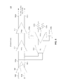
- FIG. 3 illustrates a portion of an example receiver front-end circuit 300 according to an embodiment of the present disclosure.
- Example circuit 300 is provided for the purpose of illustration only and is not limiting of embodiments of the present disclosure.
- receiver front-end circuit 300 includes peaking equalizer 102 , amplifiers 302 and 304 , capacitors 306 a - b and 308 a - b , and a capacitively-degenerated cross-coupled differential pair circuit 310 .
- Peaking equalizer 102 is configured to receive differential input data signals 104 a and 104 b , and to generate differential output data signals 106 a and 106 b .
- Differential output data signals 106 a and 106 b are coupled to amplifiers 302 and 304 , before being provided to other circuitry, such as data slicers, for example.
- Capacitors 306 a - b couple the input terminals and the output terminals of amplifier 302 in a positive feedback manner. As such, for each respectively coupled input terminal and output terminal, a portion of the output signal adds in phase with the input signal, augmenting the input signal (e.g., loop gain is positive). Capacitors 308 a - b couple the input terminals and the output terminals of amplifier 304 in a positive feedback manner. Circuit 310 is coupled to the output terminals of amplifier 304 . In an embodiments, capacitors 306 a - b and 308 a - b are floating metal capacitors.
- example circuit 300 does not use inductors for bandwidth extension of equalizer 102 , amplifier 302 , and amplifier 304 . Instead, as further described below, example circuit 300 relies on amplifier 302 and capacitors 306 a - b to extend the bandwidth of equalizer 102 , on amplifier 304 and capacitors 308 a - b to extend the bandwidth of amplifier 302 , and on circuit 310 to extend the bandwidth of amplifier 304 .
- embodiments operate by emulating a negative capacitance at the output of a stage whose bandwidth is being extended.
- amplifier 302 and capacitors 306 a - b are configured to emulate the presence of a negative capacitance at the outputs of equalizer 102 .
- amplifier 304 and capacitors 308 a - b are configured to emulate the presence of a negative capacitance at the outputs of amplifier 302 .
- This negative capacitance is due to the Miller effect created by the coupling of capacitors 306 a - b (capacitors 308 a - b ) in a positive feedback around amplifier 302 (amplifier 304 ).
- the Miller effect of this coupling is further described below with respect to an example 400 shown in FIG. 4 .
- FIG. 4 is an example 400 that illustrates the Miller effect with respect to an example amplifier according to an embodiment of the present disclosure.
- example 400 illustrates the equivalent circuit of the circuit structure comprised of amplifier 302 and capacitor 306 a , coupled around amplifier 302 in a positive feedback manner.
- the equivalent circuit includes amplifier 302 , a first Miller capacitance 402 , coupled as an input capacitance at an input terminal of amplifier 302 , and a second Miller capacitance 404 , coupled as an output capacitance at an output terminal of amplifier 302 .
- the value of first capacitance 402 is given by C(1 ⁇ A v ), where C is the capacitance of capacitor 306 a and A v , is the gain of amplifier 302 .
- the value of second capacitance 404 is given by C(1 ⁇ 1/A v ).
- the equivalent circuit includes a negative Miller capacitance and a positive Miller capacitance.
- amplifier 302 and capacitors 306 a - b are configured to produce a negative capacitance at each output of equalizer 102 .
- the configuration involves selecting an appropriate gain A v of amplifier 302 and an appropriate value for capacitors 306 a - b such that the resultant Miller negative capacitance (e.g., equivalent to first capacitance 402 in FIG. 4 ) is equal or substantially equal (in absolute value) to the output load capacitance of equalizer 102 (e.g., equivalent to capacitor 202 in FIG. 2 ).
- amplifier 302 and capacitors 306 a - b are configured to produce a negative capacitance that is slightly lower (in absolute value) than the output load capacitance of equalizer 102 . This prevents the negative capacitance from exceeding (e.g., due temperature, process, and part-to-part variations) the output load capacitance being compensated and equalizer 102 from exhibiting peaking behaviors (where high frequencies are amplified significantly more than lower frequencies).
- amplifier 304 and capacitors 308 a - b are configured to produce a negative capacitance at each output of amplifier 302 .
- the configuration involves selecting an appropriate gain A v of amplifier 304 and an appropriate value for capacitors 308 a - b such that the resultant negative capacitance (e.g., equivalent to first capacitance 402 in FIG. 4 ) is equal or substantially equal (in absolute value) to a combined capacitance of the output load capacitance of amplifier 302 (e.g., equivalent to capacitor 202 in FIG. 2 ) and the positive capacitance (e.g., equivalent to second capacitance 404 ) created by amplifier 302 and capacitors 306 a - b.
- the resultant negative capacitance e.g., equivalent to first capacitance 402 in FIG. 4
- the positive capacitance e.g., equivalent to second capacitance 404
- amplifier 304 and capacitors 308 a - b are configured to produce a negative capacitance that is slightly lower (in absolute value) than the combined capacitance, to prevent the negative capacitance from exceeding (e.g., due temperature, process, and part-to-part variations) the combined capacitance and amplifier 304 from exhibiting peaking behaviors (where high frequencies are amplified significantly more than lower frequencies).
- example circuit 300 may include any number of equalizers, such as equalizer 102 , and amplifiers, such as amplifiers 302 and 304 , with each stage (e.g., amplifier 302 or 304 ) used to extend the bandwidth of the stage (or stages) that precedes it by reducing or cancelling its output load capacitance.
- This approach can thus be used to extend the bandwidth of every stage of a receiver front-end circuit, except for the final stage (e.g., amplifier 304 ), which is typically followed by a bit slicer, for example.
- the bandwidth of the final amplifier stage 304 is extended using a circuit 310 , coupled to the output terminals of amplifier 304 .
- Circuit 310 emulates the presence of a negative capacitance at each output terminal of amplifier 304 .
- the negative capacitance is equal or substantially equal to a combined capacitance of the output load capacitance of amplifier 304 (e.g., capacitor 202 in FIG. 2 ) and the positive capacitance (e.g., second capacitance 404 ) created by amplifier 304 and capacitors 308 a - b .
- circuit 310 includes a cross-coupled NMOS differential pair 312 a - b , current sources 316 a - b , and degenerating capacitor 314 .
- Differential pair transistors 312 a - b are capacitively-degenerated by capacitor 314 .
- receiver front-end circuits may require compensation of device offsets. Since device offsets typically change over voltage, temperature, and time, the offset compensation should adjust its correction in a continuous manner. Conventionally, offset compensation is provided by an analog feedback loop. Accordingly, the feedback loop is maintained continuously on, which results in significant power consumption. Further, to reduce the bandwidth of the feedback loop (to pass DC only), large capacitors are typically used in the loop, thus also requiring a large area for the loop circuit implementation.
- FIG. 5 illustrates a portion of a conventional receiver front-end circuit 500 .
- receiver front-end circuit 500 includes a peaking equalizer 102 , followed by a plurality of amplifiers 110 and 114 .
- Peaking equalizer 102 is configured to receive differential input data signals 104 a and 104 b , and to generate differential output data signals 106 a and 106 b .
- Differential output data signals 106 a and 106 b are coupled to amplifiers 110 and 114 , before being provided to other circuitry, such as data slicers, for example.
- Amplifiers 110 and 114 may be limiting amplifiers, configured to attenuate the portions of signals 106 a and 106 b that are above a certain level, in order to prevent saturation of subsequent stages.
- Circuit 500 further includes an analog feedback loop to provide offset compensation.
- the analog feedback loop includes resistors 504 a - b , an amplifier 506 , capacitors 508 a - b , and a transconductance stage 510 .
- Resistors 504 a - b couple outputs 502 a - b of amplifier 114 to respective input terminals of amplifier 506 .
- Capacitors 508 a - b couple respective input terminals of amplifier 506 to respective output terminals of amplifier 506 .
- Transconductance stage 510 is coupled between output terminals of amplifier 506 and input ten finals of amplifier 110 .
- capacitors 508 a - b are selected to be relatively large in order to reduce the bandwidth of the analog feedback loop, thereby passing DC components only of outputs 502 a - b of amplifier 114 .
- the analog feedback loop is both power consuming and large in area.
- Embodiments of the present disclosure enable DC offset compensation with the use of a digital feedback loop.
- the feedback loop can be turned on/off as needed, reducing its power consumption.
- large area capacitors can be eliminated, leading to a reduced circuit implementation size.
- FIG. 6 illustrates a portion of a receiver circuit 600 according to an embodiment of the present disclosure.
- Example circuit 600 is provided for the purpose of illustration only and is not limiting of embodiments of the present disclosure.
- circuit 600 includes equalizer 102 , amplifiers 110 and 114 , a slicer module 602 , a digital offset correction module 604 , and a current digital-to-analog converter (DAC) 610 .
- equalizer 102 equalizer 102
- amplifiers 110 and 114 includes equalizer 102 , amplifiers 110 and 114 , a slicer module 602 , a digital offset correction module 604 , and a current digital-to-analog converter (DAC) 610 .
- DAC current digital-to-analog converter
- amplifiers 110 and 114 may be replaced with the circuit structure provided by amplifiers 302 and 304 , capacitors 306 a - b and 308 a - b , and circuit 310 described above in FIG. 3 , in order to extend the bandwidth of the receiver front-end portion of receiver circuit 600 .
- offset compensation in receiver circuit 600 is performed in the digital domain. Accordingly, the outputs of amplifier 114 are first provided to slicer module 602 .
- Slicer module 602 may include a bit slicer 612 and a demultiplexer 614 .
- Bit slicer 612 generates soft/hard bit decisions based on the outputs of amplifier 114 and provides the bit decisions to demultiplexer 614 .
- Demultiplexer 614 demultiplexes the bit decisions into a parallel bit steam 606 , which is then provided to digital offset correction module 604 .
- Digital offset correction module 604 together with current DAC 610 , form a digital feedback loop.
- digital offset correction module 604 is configured to determine the presence of DC offset based on parallel bit stream 606 .
- module 604 determines the presence of DC offset by monitoring the long-term DC-balance of bit stream 606 .
- data being received by circuit 600 is DC balanced (e.g., the data includes equal or approximately equal numbers of 0's and 1's over a long time interval) due to applied line coding. A DC-unbalance is attributed to the presence of DC offset in the received data.
- module 604 is configured to monitor bit stream 606 over a pre-determined time interval and to determine whether or not bit stream 606 is DC-balanced over the pre-determined time interval.
- the pre-determined time interval is selected based on the line coding applied to the received data.
- bit slicer 612 is part of a clock and data recovery (CDR) timing loop.
- CDR timing loop locks to the input signal phase
- bit sheet 612 samples the output of amplifier 114 with the clock aligned with data transition edges. If an offset exists in the output of amplifier 114 , it will result in an unbalanced number of 0s and 1s in the output of bit slicer 612 .
- Module 604 uses this information to determine the direction and amount of correction needed.
- digital module 604 determines a DC-unbalance (e.g., above a pre-determined threshold) in bit stream 606 , digital module 604 generates and provides a digital offset code 608 to current DAC 610 .
- Digital offset code 608 controls DAC 610 to generate a current 616 .
- Current 616 is applied at the input of amplifier 110 , and is configured to reduce the presence of DC offset at the input of amplifier 110 . In other embodiments, current 616 may be applied to the input of equalizer 102 or amplifier 114 .
- digital module 604 implements hysteresis such that the digital feedback loop is turned off when the DC offset is within a pre-determined range and turned on when the DC offset is outside of the pre-determined range.
- the digital feedback loop is disabled when the offset is within ⁇ 1 ⁇ 2 LSB (least significant bit). This hysteresis implementation prevents excessive corrections that add jitter and degrade the signal waveform at 106 a - b.
Landscapes
- Engineering & Computer Science (AREA)
- Computer Networks & Wireless Communication (AREA)
- Signal Processing (AREA)
- Amplifiers (AREA)
Abstract
Description
Claims (20)
Priority Applications (5)
| Application Number | Priority Date | Filing Date | Title |
|---|---|---|---|
| US13/567,721 US9136904B2 (en) | 2012-08-06 | 2012-08-06 | High bandwidth equalizer and limiting amplifier |
| EP13003596.7A EP2696511B1 (en) | 2012-08-06 | 2013-07-17 | High Bandwidth equalizer and limiting amplifier |
| TW102127522A TWI535225B (en) | 2012-08-06 | 2013-07-31 | High bandwidth equalizer and limiting amplifier |
| KR20130093136A KR20140019246A (en) | 2012-08-06 | 2013-08-06 | High bandwidth equalizer and limiting amplifier |
| CN201310339818.1A CN103580620B (en) | 2012-08-06 | 2013-08-06 | High bandwidth equalizer and limiting amplifier |
Applications Claiming Priority (1)
| Application Number | Priority Date | Filing Date | Title |
|---|---|---|---|
| US13/567,721 US9136904B2 (en) | 2012-08-06 | 2012-08-06 | High bandwidth equalizer and limiting amplifier |
Publications (2)
| Publication Number | Publication Date |
|---|---|
| US20140036982A1 US20140036982A1 (en) | 2014-02-06 |
| US9136904B2 true US9136904B2 (en) | 2015-09-15 |
Family
ID=48795393
Family Applications (1)
| Application Number | Title | Priority Date | Filing Date |
|---|---|---|---|
| US13/567,721 Active 2033-02-20 US9136904B2 (en) | 2012-08-06 | 2012-08-06 | High bandwidth equalizer and limiting amplifier |
Country Status (5)
| Country | Link |
|---|---|
| US (1) | US9136904B2 (en) |
| EP (1) | EP2696511B1 (en) |
| KR (1) | KR20140019246A (en) |
| CN (1) | CN103580620B (en) |
| TW (1) | TWI535225B (en) |
Cited By (2)
| Publication number | Priority date | Publication date | Assignee | Title |
|---|---|---|---|---|
| US20210091736A1 (en) * | 2019-09-19 | 2021-03-25 | Global Unichip Corporation | Amplifier device and offset cancellation method |
| US10979256B2 (en) | 2018-10-15 | 2021-04-13 | Shanghai Zhaoxin Semiconductor Co., Ltd. | Receiving circuits and methods for increasing bandwidth |
Families Citing this family (13)
| Publication number | Priority date | Publication date | Assignee | Title |
|---|---|---|---|---|
| US9184957B2 (en) | 2012-12-27 | 2015-11-10 | Intel Corporation | High speed receivers circuits and methods |
| KR102219849B1 (en) * | 2014-01-03 | 2021-02-24 | 삼성전자주식회사 | Apparatus and method for calibration of a direct current offset in a direct conversion receiver |
| US11162591B2 (en) * | 2016-03-10 | 2021-11-02 | General Electric Company | Seal ring assembly for a dynamoelectric machine |
| CN108880543B (en) * | 2017-05-10 | 2022-04-01 | 深圳清华大学研究院 | Pipeline analog-to-digital converter and operational amplifier self-adaptive configuration circuit and method thereof |
| KR20180062356A (en) * | 2017-11-16 | 2018-06-08 | 서울과학기술대학교 산학협력단 | Adaptive equalizing circuit |
| US20200412316A1 (en) * | 2018-03-07 | 2020-12-31 | Xiamen Ux High-Speed Ic Co., Ltd. | Low-voltage high-speed programmable equalization circuit |
| US11165456B2 (en) | 2018-04-03 | 2021-11-02 | Semiconductor Components Industries, Llc | Methods and apparatus for a continuous time linear equalizer |
| TWI673960B (en) * | 2018-11-29 | 2019-10-01 | Yuan Ze University | Tuning method for improving the quality of broadband RF signals |
| KR102684575B1 (en) * | 2019-02-26 | 2024-07-15 | 에스케이하이닉스 주식회사 | Signal receiver circuit, semiconductor apparatus and semiconductor system including the same |
| WO2021145109A1 (en) * | 2020-01-16 | 2021-07-22 | ソニーセミコンダクタソリューションズ株式会社 | Reception circuit |
| TWI779503B (en) * | 2021-02-25 | 2022-10-01 | 瑞昱半導體股份有限公司 | Image signal transmission apparatus and signal output circuit having bandwidth broadening mechanism thereof |
| US11689201B2 (en) * | 2021-07-26 | 2023-06-27 | Qualcomm Incorporated | Universal serial bus (USB) host data switch with integrated equalizer |
| US20240162874A1 (en) * | 2022-11-16 | 2024-05-16 | Qualcomm Incorporated | Second-Order Equalizer for High-Speed Data Lines |
Citations (10)
| Publication number | Priority date | Publication date | Assignee | Title |
|---|---|---|---|---|
| US20020122504A1 (en) * | 2001-01-04 | 2002-09-05 | Koninklijke Philips Electronics N.V. | Receiver having a variable threshold slicer stage and a method of updating the threshold levels of the slicer stage |
| US6542540B1 (en) * | 1998-12-21 | 2003-04-01 | Analog Devices, Inc. | Integrated analog adaptive equalizer |
| US20030102908A1 (en) * | 2000-06-28 | 2003-06-05 | Udo Ausserlechner | Frequency-compensated, multistage amplifier configuration and method for operating a frequency-compensated amplifier configuration |
| EP1447950A1 (en) | 2003-02-14 | 2004-08-18 | Vrije Universiteit Brussel | Low voltage adaptive equalizer |
| EP1622285A2 (en) | 2004-07-09 | 2006-02-01 | Vrije Universiteit Brussel | Multistage equalizer |
| US20090273370A1 (en) * | 2006-06-28 | 2009-11-05 | Nxp B.V. | Muller-C Element |
| US20100194478A1 (en) * | 2007-07-20 | 2010-08-05 | Xavier Maillard | Equalizer filter with mismatch tolerant detection mechanism for lower and higher frequency gain loops |
| EP2369742A1 (en) | 2010-03-23 | 2011-09-28 | Northrop Grumman LITEF GmbH | Amplifier circuit and method for conditioning an output current signal of a detecting element |
| US20110234312A1 (en) * | 2010-03-24 | 2011-09-29 | Texas Instruments Incorporated | Amplifier with improved stability |
| US20120299654A1 (en) * | 2010-05-06 | 2012-11-29 | Zhaozheng Hou | Power amplifier and method for amplifying signal based on power amplifier |
Family Cites Families (2)
| Publication number | Priority date | Publication date | Assignee | Title |
|---|---|---|---|---|
| TW440767B (en) * | 1998-06-02 | 2001-06-16 | Fujitsu Ltd | Method of and apparatus for correctly transmitting signals at high speed without waveform distortion |
| US6731163B2 (en) * | 2002-03-08 | 2004-05-04 | Texas Instruments Incorporated | Miller de-compensation for differential input, differential output amplifier |
-
2012
- 2012-08-06 US US13/567,721 patent/US9136904B2/en active Active
-
2013
- 2013-07-17 EP EP13003596.7A patent/EP2696511B1/en active Active
- 2013-07-31 TW TW102127522A patent/TWI535225B/en not_active IP Right Cessation
- 2013-08-06 KR KR20130093136A patent/KR20140019246A/en not_active Application Discontinuation
- 2013-08-06 CN CN201310339818.1A patent/CN103580620B/en not_active Expired - Fee Related
Patent Citations (13)
| Publication number | Priority date | Publication date | Assignee | Title |
|---|---|---|---|---|
| US6542540B1 (en) * | 1998-12-21 | 2003-04-01 | Analog Devices, Inc. | Integrated analog adaptive equalizer |
| US20030102908A1 (en) * | 2000-06-28 | 2003-06-05 | Udo Ausserlechner | Frequency-compensated, multistage amplifier configuration and method for operating a frequency-compensated amplifier configuration |
| US20020122504A1 (en) * | 2001-01-04 | 2002-09-05 | Koninklijke Philips Electronics N.V. | Receiver having a variable threshold slicer stage and a method of updating the threshold levels of the slicer stage |
| EP1447950A1 (en) | 2003-02-14 | 2004-08-18 | Vrije Universiteit Brussel | Low voltage adaptive equalizer |
| EP1622285A2 (en) | 2004-07-09 | 2006-02-01 | Vrije Universiteit Brussel | Multistage equalizer |
| US20090273370A1 (en) * | 2006-06-28 | 2009-11-05 | Nxp B.V. | Muller-C Element |
| US20100194478A1 (en) * | 2007-07-20 | 2010-08-05 | Xavier Maillard | Equalizer filter with mismatch tolerant detection mechanism for lower and higher frequency gain loops |
| EP2369742A1 (en) | 2010-03-23 | 2011-09-28 | Northrop Grumman LITEF GmbH | Amplifier circuit and method for conditioning an output current signal of a detecting element |
| CN102281035A (en) | 2010-03-23 | 2011-12-14 | 诺思罗普·格鲁曼·利特夫有限责任公司 | Amplifier circuit and method for conditioning an output current signal of a detecting element |
| US20120326779A1 (en) * | 2010-03-23 | 2012-12-27 | Ernst Rau | Amplifier circuit and method for conditioning an output current signal of a detector element |
| US8466748B2 (en) | 2010-03-23 | 2013-06-18 | Northrop Grumman Litef Gmbh | Amplifier circuit and method for conditioning an output current signal of a detector element |
| US20110234312A1 (en) * | 2010-03-24 | 2011-09-29 | Texas Instruments Incorporated | Amplifier with improved stability |
| US20120299654A1 (en) * | 2010-05-06 | 2012-11-29 | Zhaozheng Hou | Power amplifier and method for amplifying signal based on power amplifier |
Non-Patent Citations (3)
| Title |
|---|
| European Search Report directed toward European Patent Application No. 13003596.7, dated Dec. 3, 2013, European Patent Office, The Hague; 3 pages. |
| Korean Office Action directed toward related KR Application No. 10-2013-0093136, dated Jul. 25, 2014 from the Korean Intellectual Property Office; 9 pages. |
| Office Action directed to related Taiwanese Patent Application No. 102127522, mailed Feb. 12, 2015. 6 pages. |
Cited By (3)
| Publication number | Priority date | Publication date | Assignee | Title |
|---|---|---|---|---|
| US10979256B2 (en) | 2018-10-15 | 2021-04-13 | Shanghai Zhaoxin Semiconductor Co., Ltd. | Receiving circuits and methods for increasing bandwidth |
| US20210091736A1 (en) * | 2019-09-19 | 2021-03-25 | Global Unichip Corporation | Amplifier device and offset cancellation method |
| US11101781B2 (en) * | 2019-09-19 | 2021-08-24 | Global Unichip Corporation | Amplifier device and offset cancellation method |
Also Published As
| Publication number | Publication date |
|---|---|
| CN103580620B (en) | 2016-12-28 |
| US20140036982A1 (en) | 2014-02-06 |
| KR20140019246A (en) | 2014-02-14 |
| EP2696511B1 (en) | 2018-09-19 |
| EP2696511A1 (en) | 2014-02-12 |
| TWI535225B (en) | 2016-05-21 |
| CN103580620A (en) | 2014-02-12 |
| TW201412032A (en) | 2014-03-16 |
Similar Documents
| Publication | Publication Date | Title |
|---|---|---|
| US9136904B2 (en) | High bandwidth equalizer and limiting amplifier | |
| EP3437187B1 (en) | System and method for controlling common mode voltage via replica circuit and feedback control | |
| US7538606B2 (en) | Constant bandwidth DC offset correction in an amplifier | |
| KR101127461B1 (en) | Highly Linear Variable Gain Amplifier | |
| US8410846B2 (en) | Variable gain amplifier | |
| US10637695B1 (en) | High-speed low-voltage serial link receiver and method thereof | |
| US20090072861A1 (en) | Wireline transmission circuit | |
| US7969218B2 (en) | Receiver for reducing intersymbol interference of a channel and compensating for signal gain loss, and method thereof | |
| US9800218B1 (en) | Apparatus and method for correcting baseline wander and offset insertion in AC coupling circuits | |
| US20110133837A1 (en) | Variable gain amplifier | |
| US6538513B2 (en) | Common mode output current control circuit and method | |
| US7532045B1 (en) | Low-complexity active transconductance circuit | |
| US11522505B2 (en) | Semiconductor integrated circuit and receiver device | |
| EP1435693A1 (en) | Amplification circuit | |
| CN113497603B (en) | Device for baseline wander correction by means of differential wander current sensing | |
| JP2010220195A (en) | Current conveyor based instrumentation amplifier | |
| US7633343B2 (en) | Fully differential amplifier | |
| US20180069514A1 (en) | Low voltage high speed cmos line driver without tail current source | |
| US8633767B2 (en) | Amplifier circuit with noise suppression and related noise suppression method thereof | |
| US9871495B2 (en) | Thermal compensation for amplifiers | |
| US7312658B2 (en) | Differential amplifier with two outputs and a single input of improved linearity | |
| US11349442B2 (en) | Low-noise differential to single-ended converter | |
| WO2021124450A1 (en) | Differential amplification circuit, reception circuit and semiconductor integrated circuit | |
| JP4369820B2 (en) | Switched capacitor amplifier circuit | |
| WO2018180111A1 (en) | Noise removal circuit |
Legal Events
| Date | Code | Title | Description |
|---|---|---|---|
| AS | Assignment |
Owner name: BROADCOM CORPORATION, CALIFORNIA Free format text: ASSIGNMENT OF ASSIGNORS INTEREST;ASSIGNORS:ALI, TAMER;NAZEMI, ALI;KOCAMAN, NAMIK;SIGNING DATES FROM 20120801 TO 20120802;REEL/FRAME:028732/0052 |
|
| STCF | Information on status: patent grant |
Free format text: PATENTED CASE |
|
| AS | Assignment |
Owner name: BANK OF AMERICA, N.A., AS COLLATERAL AGENT, NORTH CAROLINA Free format text: PATENT SECURITY AGREEMENT;ASSIGNOR:BROADCOM CORPORATION;REEL/FRAME:037806/0001 Effective date: 20160201 Owner name: BANK OF AMERICA, N.A., AS COLLATERAL AGENT, NORTH Free format text: PATENT SECURITY AGREEMENT;ASSIGNOR:BROADCOM CORPORATION;REEL/FRAME:037806/0001 Effective date: 20160201 |
|
| AS | Assignment |
Owner name: AVAGO TECHNOLOGIES GENERAL IP (SINGAPORE) PTE. LTD., SINGAPORE Free format text: ASSIGNMENT OF ASSIGNORS INTEREST;ASSIGNOR:BROADCOM CORPORATION;REEL/FRAME:041706/0001 Effective date: 20170120 Owner name: AVAGO TECHNOLOGIES GENERAL IP (SINGAPORE) PTE. LTD Free format text: ASSIGNMENT OF ASSIGNORS INTEREST;ASSIGNOR:BROADCOM CORPORATION;REEL/FRAME:041706/0001 Effective date: 20170120 |
|
| AS | Assignment |
Owner name: BROADCOM CORPORATION, CALIFORNIA Free format text: TERMINATION AND RELEASE OF SECURITY INTEREST IN PATENTS;ASSIGNOR:BANK OF AMERICA, N.A., AS COLLATERAL AGENT;REEL/FRAME:041712/0001 Effective date: 20170119 |
|
| AS | Assignment |
Owner name: AVAGO TECHNOLOGIES INTERNATIONAL SALES PTE. LIMITE Free format text: MERGER;ASSIGNOR:AVAGO TECHNOLOGIES GENERAL IP (SINGAPORE) PTE. LTD.;REEL/FRAME:047229/0408 Effective date: 20180509 |
|
| AS | Assignment |
Owner name: AVAGO TECHNOLOGIES INTERNATIONAL SALES PTE. LIMITE Free format text: CORRECTIVE ASSIGNMENT TO CORRECT THE EFFECTIVE DATE PREVIOUSLY RECORDED ON REEL 047229 FRAME 0408. ASSIGNOR(S) HEREBY CONFIRMS THE THE EFFECTIVE DATE IS 09/05/2018;ASSIGNOR:AVAGO TECHNOLOGIES GENERAL IP (SINGAPORE) PTE. LTD.;REEL/FRAME:047349/0001 Effective date: 20180905 |
|
| MAFP | Maintenance fee payment |
Free format text: PAYMENT OF MAINTENANCE FEE, 4TH YEAR, LARGE ENTITY (ORIGINAL EVENT CODE: M1551); ENTITY STATUS OF PATENT OWNER: LARGE ENTITY Year of fee payment: 4 |
|
| AS | Assignment |
Owner name: AVAGO TECHNOLOGIES INTERNATIONAL SALES PTE. LIMITE Free format text: CORRECTIVE ASSIGNMENT TO CORRECT THE PATENT NUMBER 9,385,856 TO 9,385,756 PREVIOUSLY RECORDED AT REEL: 47349 FRAME: 001. ASSIGNOR(S) HEREBY CONFIRMS THE MERGER;ASSIGNOR:AVAGO TECHNOLOGIES GENERAL IP (SINGAPORE) PTE. LTD.;REEL/FRAME:051144/0648 Effective date: 20180905 |
|
| MAFP | Maintenance fee payment |
Free format text: PAYMENT OF MAINTENANCE FEE, 8TH YEAR, LARGE ENTITY (ORIGINAL EVENT CODE: M1552); ENTITY STATUS OF PATENT OWNER: LARGE ENTITY Year of fee payment: 8 |