WO2021124450A1 - Differential amplification circuit, reception circuit and semiconductor integrated circuit - Google Patents
Differential amplification circuit, reception circuit and semiconductor integrated circuit Download PDFInfo
- Publication number
- WO2021124450A1 WO2021124450A1 PCT/JP2019/049423 JP2019049423W WO2021124450A1 WO 2021124450 A1 WO2021124450 A1 WO 2021124450A1 JP 2019049423 W JP2019049423 W JP 2019049423W WO 2021124450 A1 WO2021124450 A1 WO 2021124450A1
- Authority
- WO
- WIPO (PCT)
- Prior art keywords
- replica
- transistor
- gate
- drain
- amplifier circuit
- Prior art date
Links
Images


Classifications
-
- H—ELECTRICITY
- H03—ELECTRONIC CIRCUITRY
- H03F—AMPLIFIERS
- H03F3/00—Amplifiers with only discharge tubes or only semiconductor devices as amplifying elements
- H03F3/45—Differential amplifiers
- H03F3/45071—Differential amplifiers with semiconductor devices only
- H03F3/45076—Differential amplifiers with semiconductor devices only characterised by the way of implementation of the active amplifying circuit in the differential amplifier
- H03F3/45179—Differential amplifiers with semiconductor devices only characterised by the way of implementation of the active amplifying circuit in the differential amplifier using MOSFET transistors as the active amplifying circuit
-
- H—ELECTRICITY
- H04—ELECTRIC COMMUNICATION TECHNIQUE
- H04L—TRANSMISSION OF DIGITAL INFORMATION, e.g. TELEGRAPHIC COMMUNICATION
- H04L25/00—Baseband systems
- H04L25/02—Details ; arrangements for supplying electrical power along data transmission lines
- H04L25/03—Shaping networks in transmitter or receiver, e.g. adaptive shaping networks
- H04L25/03006—Arrangements for removing intersymbol interference
- H04L25/03012—Arrangements for removing intersymbol interference operating in the time domain
- H04L25/03114—Arrangements for removing intersymbol interference operating in the time domain non-adaptive, i.e. not adjustable, manually adjustable, or adjustable only during the reception of special signals
- H04L25/03146—Arrangements for removing intersymbol interference operating in the time domain non-adaptive, i.e. not adjustable, manually adjustable, or adjustable only during the reception of special signals with a recursive structure
-
- H—ELECTRICITY
- H03—ELECTRONIC CIRCUITRY
- H03F—AMPLIFIERS
- H03F1/00—Details of amplifiers with only discharge tubes, only semiconductor devices or only unspecified devices as amplifying elements
- H03F1/30—Modifications of amplifiers to reduce influence of variations of temperature or supply voltage or other physical parameters
- H03F1/301—Modifications of amplifiers to reduce influence of variations of temperature or supply voltage or other physical parameters in MOSFET amplifiers
-
- H—ELECTRICITY
- H03—ELECTRONIC CIRCUITRY
- H03F—AMPLIFIERS
- H03F3/00—Amplifiers with only discharge tubes or only semiconductor devices as amplifying elements
- H03F3/189—High frequency amplifiers, e.g. radio frequency amplifiers
- H03F3/19—High frequency amplifiers, e.g. radio frequency amplifiers with semiconductor devices only
- H03F3/195—High frequency amplifiers, e.g. radio frequency amplifiers with semiconductor devices only in integrated circuits
-
- H—ELECTRICITY
- H03—ELECTRONIC CIRCUITRY
- H03F—AMPLIFIERS
- H03F3/00—Amplifiers with only discharge tubes or only semiconductor devices as amplifying elements
- H03F3/45—Differential amplifiers
- H03F3/45071—Differential amplifiers with semiconductor devices only
- H03F3/45076—Differential amplifiers with semiconductor devices only characterised by the way of implementation of the active amplifying circuit in the differential amplifier
- H03F3/45179—Differential amplifiers with semiconductor devices only characterised by the way of implementation of the active amplifying circuit in the differential amplifier using MOSFET transistors as the active amplifying circuit
- H03F3/45197—Pl types
- H03F3/45201—Non-folded cascode stages
-
- H—ELECTRICITY
- H03—ELECTRONIC CIRCUITRY
- H03F—AMPLIFIERS
- H03F3/00—Amplifiers with only discharge tubes or only semiconductor devices as amplifying elements
- H03F3/45—Differential amplifiers
- H03F3/45071—Differential amplifiers with semiconductor devices only
- H03F3/45479—Differential amplifiers with semiconductor devices only characterised by the way of common mode signal rejection
- H03F3/45632—Differential amplifiers with semiconductor devices only characterised by the way of common mode signal rejection in differential amplifiers with FET transistors as the active amplifying circuit
- H03F3/45636—Differential amplifiers with semiconductor devices only characterised by the way of common mode signal rejection in differential amplifiers with FET transistors as the active amplifying circuit by using feedback means
-
- H—ELECTRICITY
- H04—ELECTRIC COMMUNICATION TECHNIQUE
- H04L—TRANSMISSION OF DIGITAL INFORMATION, e.g. TELEGRAPHIC COMMUNICATION
- H04L25/00—Baseband systems
- H04L25/02—Details ; arrangements for supplying electrical power along data transmission lines
- H04L25/0264—Arrangements for coupling to transmission lines
- H04L25/0272—Arrangements for coupling to multiple lines, e.g. for differential transmission
-
- H—ELECTRICITY
- H03—ELECTRONIC CIRCUITRY
- H03F—AMPLIFIERS
- H03F2200/00—Indexing scheme relating to amplifiers
- H03F2200/453—Controlling being realised by adding a replica circuit or by using one among multiple identical circuits as a replica circuit
-
- H—ELECTRICITY
- H03—ELECTRONIC CIRCUITRY
- H03F—AMPLIFIERS
- H03F2200/00—Indexing scheme relating to amplifiers
- H03F2200/75—Indexing scheme relating to amplifiers the amplifier stage being a common source configuration MOSFET
-
- H—ELECTRICITY
- H03—ELECTRONIC CIRCUITRY
- H03F—AMPLIFIERS
- H03F2203/00—Indexing scheme relating to amplifiers with only discharge tubes or only semiconductor devices as amplifying elements covered by H03F3/00
- H03F2203/45—Indexing scheme relating to differential amplifiers
- H03F2203/45374—Indexing scheme relating to differential amplifiers the AAC comprising one or more discrete resistors
Definitions
- the present invention relates to a differential amplifier circuit, a receiving circuit and a semiconductor integrated circuit.
- Patent Document 1 discloses a high-speed differential amplifier having a differential amplifier and a control signal generator.
- the differential amplifier amplifies the voltage difference between the first input signal and the second input signal to generate an output signal.
- the control signal generator includes a replica differential amplifier, which is a replica of the differential amplifier, and generates a control signal that controls the gain of the differential amplifier and the replica differential amplifier.
- Patent Document 2 discloses a gain amplifier having a first transistor, a second transistor, a register, and a third transistor.
- the first transistor has a first control port, a first input port, and a first output port.
- the second transistor has a second control port, a second input port, and a second output port.
- the register has a first end connected to a first output port and a second end connected to a second output port.
- the third transistor is connected to the first output port and the second output port, and is connected in parallel with the register.
- Patent Document 3 discloses a variable gain amplifier circuit having a first amplifier circuit, a second amplifier circuit, a third amplifier circuit, and a current mirror circuit.
- the first amplification circuit is connected between the first and second transistors in which the differential input voltage is input to the control terminal, and between the first transistor and the second transistor, and a gain control signal is sent to the control terminal.
- An output unit that outputs the differential currents of the first output current and the second output current corresponding to the input third transistor, the current flowing through the first transistor, and the current flowing through the second transistor, respectively.
- the second amplification circuit is connected between the fourth and fifth transistors, in which the first and second voltages are input to the control terminals, respectively, and the fourth and fifth transistors, and is connected to the control terminals.
- the third amplification circuit includes the seventh and eighth transistors in which the third and fourth voltages are input to the control terminals, respectively, and the resistance element connected between the seventh transistor and the eighth transistor. It has an output unit that outputs a differential current of a third current corresponding to the current flowing through the seventh transistor and the current flowing through the eighth transistor, and a fourth current smaller than the third current, respectively. ..
- the current mirror circuit generates the above-mentioned gain control signal according to the combined current of the first current and the fourth current and the combined current of the second current and the third current.
- the gain of the differential amplifier circuit fluctuates according to the temperature.
- the parameters are used to control the gain of the differential amplifier circuit so as to be constant, there is a problem that the number of parameters increases, the control becomes complicated, and the response speed becomes low.
- An object of the present invention is to keep the gain of the differential amplifier circuit unit constant while maintaining the high speed of operation with simple control in the differential amplifier circuit.
- the differential amplification circuit includes a differential amplification circuit unit and a replica amplification circuit unit, and the differential amplification circuit unit is provided between a current source circuit and a load circuit and receives a differential input signal at a gate. It has first and second transistors that generate differential output signals at the drain and a third transistor that is connected between the sources of the first and second transistors and receives control signals at the gate.
- the replica amplification circuit unit is a replica of the voltage generation circuit that generates the first and second reference voltages and the first and second transistors, and receives the first and second reference voltages at the gate.
- a third replica transistor connected between the first and second replica transistors that generate a replica output signal at the drain and the source of the first and second replica transistors and that receives the control signal at the gate. It has an operational transistor that generates the control signal according to the difference between at least one of the first and second reference voltages and the replica output signal, and the operational amplifier has a constant gain of the replica amplification circuit unit. The control signal is generated so as to be.
- the gain of the differential amplifier circuit unit can be made constant while maintaining the high speed of operation with simple control.
- FIG. 1 is a diagram showing a configuration example of a semiconductor integrated circuit according to the first embodiment.
- FIG. 2 is a circuit diagram showing a configuration example of the differential amplifier circuit unit in the CTLE of FIG.
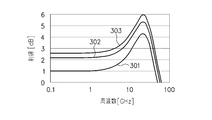
- FIG. 3 is a diagram showing the characteristics of the gain with respect to the frequency of the differential amplifier circuit unit of FIG.
- FIG. 4 is a circuit diagram showing a configuration example of the differential amplifier circuit according to the first embodiment.
- FIG. 5 is a circuit diagram showing a configuration example of the differential amplifier circuit according to the second embodiment.
- FIG. 6 is a circuit diagram showing a configuration example of the differential amplifier circuit according to the third embodiment.
- FIG. 1 is a diagram showing a configuration example of the semiconductor integrated circuit 100 according to the first embodiment.
- the semiconductor integrated circuit 100 has a receiving circuit 101 and an internal circuit 102.
- the receiving circuit 101 includes a terminal circuit 113, a continuous time linear equalizer (CTLE) 114, a determination feedback equalizer (DFE) 115, a clock generator 116, and a display. It has a multiplexer 117 and.
- CLE continuous time linear equalizer
- DFE determination feedback equalizer
- the differential input terminals 111 and 112 receive the differential signal.
- the termination circuit 113 is connected between the differential input terminals 111 and 112.
- the termination circuit 113 is composed of, for example, a resistance element.
- the CTLE 114 continuously performs equivalent processing on the time axis with respect to the differential signals received by the differential input terminals 111 and 112.
- the DFE 115 inputs the output signal of the CTLE 114, and performs equalization processing and binary determination by a feedback loop on the output signal of the CTLE 114.
- the clock generator 116 outputs a clock signal to the DFE 115.
- the demultiplexer 117 inputs the output signal of the DFE 115 and converts the output signal of the DFE 115 from serial data to parallel data.
- the internal circuit 102 processes the output signal of the demultiplexer 117.
- FIG. 2 is a circuit diagram showing a configuration example of the differential amplifier circuit unit in the CTLE 114 of FIG.
- the differential amplifier circuit unit includes current sources 201 and 202, a variable capacitance 203, resistors 204, p-channel field effect transistors 205 and 206, inductors 207 and 208, and resistors 209 and 210.
- the differential amplifier circuit unit amplifies the differential signal input to the differential input terminals Vip and Vin, and outputs the amplified differential signal from the differential output terminals Vop and Von.
- FIG. 3 is a diagram showing the characteristics of the gain with respect to the frequency of the differential amplifier circuit unit of FIG.
- the differential amplifier circuit unit is a high frequency equalizer and has a high gain in the high frequency band.
- the gain characteristic 301 is a characteristic at ⁇ 40 ° C.
- the gain characteristic 302 is a characteristic at 25 ° C.
- the gain characteristic 303 is a characteristic at 125 ° C.
- the gain of the differential amplifier circuit unit fluctuates according to the temperature. If the gain of the differential amplifier circuit unit fluctuates depending on the temperature, it causes a reception error in the reception circuit 101.
- the gain of the differential amplifier circuit unit is preferably constant regardless of the temperature.
- the differential amplifier circuit unit can control the gain in the high frequency band by controlling the value of the variable capacitance 203. Further, the differential amplifier circuit unit can control the DC gain by controlling the value of the resistor 204.
- the resistance value of the resistor 204 is made variable and the value of the resistor 204 is controlled so that the DC gain of the differential amplifier circuit unit becomes constant, the number of parameters for setting the resistance value variably increases. There is a problem that the control becomes complicated and the response speed becomes low.
- a differential amplifier circuit capable of making the DC gain of the differential amplifier circuit unit constant with simple control and at high speed will be described.
- FIG. 4 is a circuit diagram showing a configuration example of the differential amplifier circuit 400 according to the first embodiment.
- the CTLE 114 of FIG. 1 has a differential amplifier circuit 400.
- the differential amplifier circuit 400 includes a differential amplifier circuit unit 401, a replica amplifier circuit unit 402, a p-channel field effect transistor 403, an n-channel field effect transistor 404, and a BGR (bandgap reference) bias generator 405. Have.
- the differential amplifier circuit unit 401 is provided with the p-channel field effect transistors 431 and 432 corresponding to the current sources 201 and 202 in the differential amplifier circuit unit of FIG. 2, and the p-channel field effect transistor corresponding to the resistor 204 is provided. A transistor 433 is provided.
- the differential amplifier circuit unit 401 includes p-channel field-effect transistors 431 to 433, a variable capacitance 203, p-channel field-effect transistors 205 and 206, inductors 207 and 208, and resistors 209 and 210.
- the p-channel field effect transistor 431 is a current source circuit, and the source is connected to the power potential node.
- the p-channel field effect transistor 432 is a current source circuit, the source is connected to the power potential node, and the gate is connected to the gate of the p-channel field effect transistor 431.
- the variable capacitance 203 is connected between the drain of the p-channel field effect transistor 431 and the drain of the p-channel field effect transistor 432.
- the source is connected to the source of the p-channel field-effect transistor 205
- the gate is connected to the output terminal of the operational amplifier 422
- the drain is connected to the source of the p-channel field-effect transistor 206.
- the p-channel field effect transistor 433 receives a control signal output by the operational amplifier 422, and the resistance between the drain and the source changes according to the control signal.
- the source is connected to the drain of the p-channel field-effect transistor 431, the gate is connected to the differential input terminal Vip, and the drain is connected to the differential output terminal Von.
- the source is connected to the drain of the p-channel field-effect transistor 432, the gate is connected to the differential input terminal Vin, and the drain is connected to the differential output terminal Vop.
- the series connection circuit of the inductor 207 and the resistor 209 is a load circuit, and is connected between the drain of the p-channel field effect transistor 205 and the reference potential node.
- the reference potential node is, for example, a ground potential node, which is a node having a lower potential than the power potential node.
- the series connection circuit of the inductor 208 and the resistor 210 is a load circuit, and is connected between the drain of the p-channel field effect transistor 206 and the reference potential node.
- the p-channel field effects 205 and 206 receive differential input signals at the gate differential input terminals Vip and Vin, and generate differential output signals at the drain output terminals Vop and Von.
- the control signal of the gate of the p-channel field-effect transistor 433 by the operational amplifier 422, the resistance between the drain and the source of the p-channel field-effect transistor 433 is controlled, and the DC gain of the differential amplifier circuit unit 401 becomes constant. Be controlled.
- the replica amplifier circuit unit 402 is a replica of the differential amplifier circuit unit 401.
- the replica amplifier circuit unit 402 includes p-channel field effect transistors 411 to 417, resistors 418 to 421, and an operational amplifier 422.
- the p-channel field-effect transistor 412 is a replica transistor of the p-channel field-effect transistor 431, the source is connected to the power potential node, and the gate is connected to the gates of the p-channel field-effect transistors 431 and 432.
- the p-channel field-effect transistor 413 is a replica transistor of the p-channel field-effect transistor 432, the source is connected to the power potential node, and the gate is connected to the gates of the p-channel field-effect transistors 431 and 432.
- the p-channel field-effect transistor 415 is a replica transistor of the p-channel field-effect transistor 433, the source is connected to the source of the p-channel field-effect transistor 416, the gate is connected to the output terminal of the operational amplifier 422, and the drain is the p-channel field effect transistor. It is connected to the source of the effect transistor 417.
- the p-channel field-effect transistor 416 is a replica transistor of the p-channel field-effect transistor 205, and the source is connected to the drain of the p-channel field-effect transistor 412.
- the p-channel field-effect transistor 417 is a replica transistor of the p-channel field-effect transistor 206, and the source is connected to the drain of the p-channel field-effect transistor 413.
- the resistor 419 is a load circuit and is a replica of the resistor 209.
- the resistor 419 is connected between the drain of the p-channel field effect transistor 416 and the reference potential node.
- the resistor 420 is a load circuit and is a replica of the resistor 210.
- the resistor 420 is connected between the drain of the p-channel field effect transistor 417 and the reference potential node.
- the p-channel field effect transistor 411 and the resistor 418 are voltage generation circuits and generate a reference voltage V1.
- the gate of the p-channel field effect transistor 416 receives a reference voltage V1.
- the source is connected to the power potential node
- the gate is connected to the gates of the p-channel field-effect transistors 431 and 432
- the drain is connected to the gate of the p-channel field-effect transistor 416.
- the resistor 418 is connected between the drain of the p-channel field effect transistor 411 and the reference potential node.
- the p-channel field effect transistor 414 and the resistor 421 are voltage generation circuits and generate a reference voltage V2.
- the gate of the p-channel field effect transistor 417 receives a reference voltage V2.
- the source is connected to the power potential node
- the gate is connected to the gates of the p-channel field-effect transistors 431 and 432
- the drain is connected to the gate of the p-channel field-effect transistor 417.
- the resistor 421 is connected between the drain of the p-channel field effect transistor 414 and the reference potential node.
- the-input terminal is connected to the gate of the p-channel field-effect transistor 416
- the + input terminal is connected to the drain of the p-channel field-effect transistor 417
- the output terminal is connected to the gate of the p-channel field-effect transistors 415 and 433. Be connected.
- the source is connected to the power potential node, and the gate and drain are connected to each other.
- the p-channel field-effect transistor 404 has a drain connected to the drain of the p-channel field-effect transistor 403, a gate connected to the BGR bias generator 405, and a source connected to the reference potential node. Further, the gate of the p-channel field-effect transistor 403 is connected to the gate of the p-channel field-effect transistors 431 and 432.
- the BGR bias generator 405 generates a BGR (Band Gap Reference) voltage, and supplies the generated BGR voltage as a bias voltage (second bias voltage) to the gate of the p-channel field effect transistor 404.
- a bias voltage (first bias voltage) for the current source circuit is generated at the gate of the p-channel field-effect transistor 403, and the generated bias voltage is the p-channel field-effect transistor 411 to 414, 431, 432. It is supplied to each gate.
- the p-channel field effect transistors 403, 411 to 414, 431 and 432 are current mirror circuits.
- a current Ib flows through the p-channel field effect transistors 412, 413, 431 and 432.
- a current Ib ⁇ 1/2 whose current amount is 1/2 times that of the current Ib flows through the p-channel field effect transistor 414, for example, by adjusting the transistor size.
- a reference voltage V1 is input to the gate of the p-channel field effect transistor 416.
- a reference voltage V2 is input to the gate of the p-channel electric field effect transistor 417.
- the reference voltages V1 and V2 are different voltages from each other.
- the reference voltage V1 is higher than the reference voltage V2.
- the p-channel field effect transistors 416 and 417 receive reference voltages V1 and V2 at the gate and generate replica output signals V3 and V4 at the drain.
- the replica output signal V3 is a signal of the drain of the p-channel field effect transistor 417.
- the replica output signal V4 is a signal of the drain of the p-channel field effect transistor 416.
- the replica amplifier circuit unit 402 amplifies the differential input signals of the reference voltages V1 and V2, and outputs the differential output signals of the replica output signals V3 and V4. Since the replica amplifier circuit unit 402 does not have a replica of the variable capacitance 203 and the inductors 207 and 208, the gain is substantially constant with respect to the frequency.
- the operational amplifier 422 supplies a control signal to the gates of the p-channel field effect transistors 415 and 433 according to the difference between the replica output signal V3 and the reference voltage V1.
- the operational amplifier 422 generates a control signal so that the gain of the replica amplifier circuit unit 402 becomes constant.
- the operational amplifier 422 may output a control signal according to the difference between the replica output signal V4 and the reference voltage V2.
- the gain of the amplifier circuit unit 401 and the replica amplifier circuit unit 402 fluctuates depending on the temperature. For example, the gains of the amplifier circuit unit 401 and the replica amplifier circuit unit 402 increase, and the signal of the differential output terminal Vop and the replica output signal V3 increase. Then, the difference between the replica output signal V3 and the reference voltage V1 becomes large, and the control signal output by the operational amplifier 422 rises. Then, the resistance between the drain and the source of the p-channel field effect transistor 415 increases, and the gain of the replica amplifier circuit unit 402 decreases. As a result, the replica output signal V3 drops. By the above control, the operational amplifier 422 generates a control signal so that the gain of the replica amplifier circuit unit 402 becomes constant.
- the resistance between the drain and the source of the p-channel field effect transistor 433 increases, and the gain of the differential amplifier circuit unit 401 decreases. As a result, the signal of the differential output terminal Vop drops.
- the DC gain of the amplifier circuit unit 401 is controlled to be constant regardless of the temperature.
- the direct current gain of the differential amplifier circuit unit 401 can be made constant by simple control. Further, since the differential amplifier circuit unit 401 controls the gain of DC by using the p-channel field effect transistor 433, there is no element to be additionally connected to the pair of input nodes Vip and Vin, and the input load is increased. Since it does not increase, the high speed of operation can be maintained in the differential amplifier circuit 400.
- FIG. 5 is a circuit diagram showing a configuration example of the differential amplifier circuit 500 according to the second embodiment.
- the CTLE 114 of FIG. 1 has a differential amplifier circuit 500.
- the differential amplifier circuit 500 provides the differential amplifier circuit 400 of FIG. 4 with an n-channel field-effect transistor instead of the p-channel field-effect transistor and a p-channel field-effect transistor instead of the n-channel field-effect transistor. It is a transistor.
- the differential amplifier circuit 500 includes a differential amplifier circuit unit 501, a replica amplifier circuit unit 502, an n-channel field effect transistor 503, a p-channel field effect transistor 504, and a BGR bias generator 405.
- the differential amplifier circuit unit 501 includes n-channel field-effect transistors 531 to 533, variable capacitance 203, n-channel field-effect transistors 534 and 535, inductors 207 and 208, and resistors 209 and 210.
- the n-channel field effect transistor 531 is a current source circuit, and the source is connected to the reference potential node.
- the n-channel field-effect transistor 532 is a current source circuit in which the source is connected to the reference potential node and the gate is connected to the gate of the n-channel field-effect transistor 531.
- the variable capacitance 203 is connected between the drain of the n-channel field-effect transistor 531 and the drain of the n-channel field-effect transistor 532.
- the source is connected to the source of the n-channel field-effect transistor 535
- the gate is connected to the output terminal of the operational amplifier 422
- the drain is connected to the source of the n-channel field-effect transistor 534.
- the n-channel field effect transistor 533 receives a control signal output from the operational amplifier 422 at the gate, and the resistance between the drain and the source changes according to the control signal.
- the series connection circuit of the inductor 207 and the resistor 209 is a load circuit, and is connected between the drain of the n-channel field effect transistor 534 and the power potential node.
- the series connection circuit of the inductor 208 and the resistor 210 is a load circuit, and is connected between the drain of the n-channel field effect transistor 535 and the power potential node.
- the n-channel field effects 534 and 535 receive the differential input signal at the gate differential input terminals Vip and Vin, and generate the differential output signal at the drain output terminals Vop and Von.
- the control signal of the gate of the n-channel field-effect transistor 533 by the operational amplifier 422, the resistance between the drain and the source of the n-channel field-effect transistor 533 is controlled, and the DC gain of the differential amplifier circuit unit 501 becomes constant. Be controlled.
- the replica amplifier circuit unit 502 is a replica of the differential amplifier circuit unit 501.
- the replica amplifier circuit unit 502 includes n-channel field effect transistors 511 to 517, resistors 418 to 421, and an operational amplifier 422.
- the n-channel field-effect transistor 512 is a replica transistor of the n-channel field-effect transistor 531.
- the source is connected to the reference potential node, and the gate is connected to the gates of the n-channel field-effect transistors 531 and 532.
- the n-channel field-effect transistor 513 is a replica transistor of the n-channel field-effect transistor 532, with the source connected to the reference potential node and the gate connected to the gates of the n-channel field-effect transistors 531 and 532.
- the n-channel field-effect transistor 515 is a replica transistor of the n-channel field-effect transistor 533, the source is connected to the source of the n-channel field-effect transistor 517, the gate is connected to the output terminal of the operational amplifier 422, and the drain is the n-channel field effect transistor. It is connected to the source of the effect transistor 516.
- the n-channel field-effect transistor 516 is a replica transistor of the n-channel field-effect transistor 534, and the source is connected to the drain of the n-channel field-effect transistor 512.
- the n-channel field-effect transistor 517 is a replica transistor of the n-channel field-effect transistor 535, and the source is connected to the drain of the n-channel field-effect transistor 513.
- the resistor 419 is a load circuit and is a replica of the resistor 209.
- the resistor 419 is connected between the drain of the n-channel field effect transistor 516 and the power potential node.
- the resistor 420 is a load circuit and is a replica of the resistor 210.
- the resistor 420 is connected between the drain of the n-channel field effect transistor 517 and the power potential node.
- the n-channel field effect transistor 511 and the resistor 418 are voltage generation circuits and generate a reference voltage V1.
- the gate of the n-channel field effect transistor 516 receives a reference voltage V1.
- the source is connected to the reference potential node
- the gate is connected to the gates of the n-channel field-effect transistors 531 and 532
- the drain is connected to the gate of the n-channel field-effect transistor 516.
- the resistor 418 is connected between the drain of the n-channel field effect transistor 511 and the power potential node.
- the n-channel field effect transistor 514 and the resistor 421 are voltage generation circuits and generate a reference voltage V2.
- the gate of the n-channel field effect transistor 517 receives a reference voltage V2.
- the source is connected to the reference potential node
- the gate is connected to the gates of the n-channel field-effect transistors 531 and 532
- the drain is connected to the gate of the n-channel field-effect transistor 517.
- the resistor 421 is connected between the drain of the n-channel field effect transistor 514 and the power potential node.
- the-input terminal is connected to the gate of the n-channel field-effect transistor 516
- the + input terminal is connected to the drain of the n-channel field-effect transistor 517
- the output terminal is connected to the gate of the n-channel field-effect transistors 515 and 533. Be connected.
- the source is connected to the reference potential node, and the gate and drain are connected to the gate of the n-channel field-effect transistor 514.
- the drain is connected to the drain of the n-channel field effect transistor 503
- the gate is connected to the BGR bias generator 405, and the source is connected to the power potential node.
- the BGR bias generator 405 generates a BGR voltage and supplies the generated BGR voltage as a bias voltage (third bias voltage) to the n-channel field effect transistor 504 gate.
- a bias voltage (first bias voltage) for the current source circuit is generated at the gate of the n-channel field-effect transistor 503, and the generated bias voltage is the n-channel field-effect transistor 511 to 514, 513, 532. It is supplied to each gate.
- the n-channel field effect transistors 503, 511 to 514, 513 and 532 are current mirror circuits.
- a current Ib flows through the n-channel field effect transistors 512, 513, 513 and 532.
- a current Ib ⁇ 3/2 flows through the n-channel field effect transistor 511.
- a current Ib ⁇ 1/2 flows through the n-channel field effect transistor 514.
- a reference voltage V1 is input to the gate of the n-channel field effect transistor 516.
- a reference voltage V2 is input to the gate of the n-channel field effect transistor 517.
- the reference voltages V1 and V2 are different voltages from each other.
- the reference voltage V1 is lower than the reference voltage V2.
- the n-channel field effect transistors 516 and 517 receive reference voltages V1 and V2 at the gate and generate replica output signals V3 and V4 at the drain.
- the replica output signal V3 is a signal of the drain of the n-channel field effect transistor 517.
- the replica output signal V4 is a signal of the drain of the n-channel field effect transistor 516.
- the replica amplifier circuit unit 502 amplifies the differential input signals of the reference voltages V1 and V2, and outputs the differential output signals of the replica output signals V3 and V4. Since the replica amplifier circuit unit 502 does not have a replica of the variable capacitance 203 and the inductors 207 and 208, the gain is substantially constant with respect to the frequency.
- the operational amplifier 422 supplies a control signal to the gates of the n-channel field effect transistors 515 and 533 according to the difference between the replica output signal V3 and the reference voltage V1.
- the operational amplifier 422 generates a control signal so that the gain of the replica amplifier circuit unit 502 becomes constant.
- the operational amplifier 422 may output a control signal according to the difference between the replica output signal V4 and the reference voltage V2.
- the gains of the amplifier circuit unit 501 and the replica amplifier circuit unit 502 vary depending on the temperature. For example, the gains of the amplifier circuit unit 501 and the replica amplifier circuit unit 502 decrease, and the signal of the differential output terminal Vop and the replica output signal V3 increase. Then, the difference between the replica output signal V3 and the reference voltage V1 becomes large, and the control signal output by the operational amplifier 422 rises. Then, the resistance between the drain and the source of the n-channel field effect transistor 515 becomes low, and the gain of the replica amplifier circuit unit 502 increases. As a result, the replica output signal V3 drops. By the above control, the operational amplifier 422 generates a control signal so that the gain of the replica amplifier circuit unit 502 becomes constant.
- the resistance between the drain and source of the n-channel field effect transistor 533 decreases, and the gain of the differential amplifier circuit unit 501 increases. As a result, the signal of the differential output terminal Vop drops.
- the DC gain of the amplifier circuit unit 501 is controlled to be constant regardless of the temperature.
- the direct current gain of the differential amplifier circuit unit 501 can be made constant by simple control. Further, since the differential amplifier circuit unit 501 controls the gain of DC by using the n-channel field effect transistor 533, there is no element to be additionally connected to the pair of input nodes Vip and Vin, and the input load is increased. Since it does not increase, the high speed of operation can be maintained in the differential amplifier circuit 500.
- FIG. 6 is a circuit diagram showing a configuration example of the differential amplifier circuit 400 according to the third embodiment.
- the differential amplifier circuit 400 of FIG. 6 is obtained by removing the variable capacitance 203 and the inductors 207 and 208 from the differential amplifier circuit 400 of FIG.
- the resistor 209 is a load circuit and is connected between the drain of the p-channel field effect transistor 205 and the reference potential node.
- the resistor 210 is a load circuit and is connected between the drain of the p-channel field effect transistor 206 and the reference potential node.
- the gain of the differential amplifier circuit unit 401 becomes substantially constant with respect to the frequency.
- the operational amplifier 422 generates a control signal so that the gains of the differential amplifier circuit unit 401 and the replica amplifier circuit unit 402 are constant regardless of the temperature. ..
- the gain of the differential amplifier circuit unit 401 can be made constant by simple control.
- the differential amplifier circuit unit 401 controls the gain of DC by using the p-channel field effect transistor 433, there is no element to be additionally connected to the pair of input nodes Vip and Vin, and the input load is increased. Since it does not increase, the high speed of operation can be maintained in the differential amplifier circuit 400.
- variable capacitance 203 and the inductors 207 and 208 can be deleted.
- the gain of the differential amplifier circuit unit can be made constant while maintaining the high speed of operation with simple control.
Abstract
According to the present invention, a differential amplification circuit unit comprises: first and second transistors (205, 206) that are located between a current source circuit and a load circuit and receive differential input signals at the gates to generate differential output signals at the drains; and a third transistor (433) that is connected between the sources of the first and second transistors and receives a control signal at the gate, while a replica amplification circuit unit comprises: a voltage generation circuit that generates first and second reference voltages; first and second replica transistors (416, 417) that are replicas of the first and second transistors and receive the first and second reference voltages at the gates to generate replica output signals at the drains; a third replica transistor (415) that is connected between the sources of the first and second replica transistors and receives the control signal at the gate; and an operational amplifier (422) that generates the control signal in accordance with the difference between at least one of the first and second reference voltages and the replica output signal.
Description
本発明は、差動増幅回路、受信回路及び半導体集積回路に関する。
The present invention relates to a differential amplifier circuit, a receiving circuit and a semiconductor integrated circuit.
特許文献1には、差動増幅器と制御信号生成器を有する高速差動増幅器が開示されている。差動増幅器は、第1の入力信号と第2の入力信号との間の電圧差を増幅し、出力信号を生成する。制御信号生成器は、差動増幅器のレプリカであるレプリカ差動増幅器を含み、差動増幅器及びレプリカ差動増幅器の利得を制御する制御信号を生成する。
Patent Document 1 discloses a high-speed differential amplifier having a differential amplifier and a control signal generator. The differential amplifier amplifies the voltage difference between the first input signal and the second input signal to generate an output signal. The control signal generator includes a replica differential amplifier, which is a replica of the differential amplifier, and generates a control signal that controls the gain of the differential amplifier and the replica differential amplifier.
特許文献2には、第1のトランジスタと、第2のトランジスタと、レジスタと、第3のトランジスタを有する利得増幅器が開示されている。第1のトランジスタは、第1の制御ポート、第1の入力ポート、及び、第1の出力ポートを有する。第2のトランジスタは、第2の制御ポート、第2の入力ポート、及び、第2の出力ポートを有する。レジスタは、第1の出力ポートに接続された第1端、及び、第2の出力ポートに接続された第2端を有する。第3のトランジスタは、第1の出力ポート及び第2の出力ポートに接続され、かつ、レジスタと並列に接続される。第3のトランジスタに制御電圧を印加し、第1の制御ポートに入力電圧を印加したとき、第2の制御ポートは、第1の入力ポート及び第2の入力ポートにおいて、所望の出力を生成するべく、制御電圧によって選択的に修正される。
Patent Document 2 discloses a gain amplifier having a first transistor, a second transistor, a register, and a third transistor. The first transistor has a first control port, a first input port, and a first output port. The second transistor has a second control port, a second input port, and a second output port. The register has a first end connected to a first output port and a second end connected to a second output port. The third transistor is connected to the first output port and the second output port, and is connected in parallel with the register. When a control voltage is applied to the third transistor and an input voltage is applied to the first control port, the second control port produces the desired output at the first input port and the second input port. Therefore, it is selectively corrected by the control voltage.
特許文献3には、第1の増幅回路と、第2の増幅回路と、第3の増幅回路と、カレントミラー回路とを有する可変利得増幅回路が開示されている。第1の増幅回路は、差動入力電圧が制御端子に入力される第1及び第2のトランジスタと、第1のトランジスタと第2のトランジスタとの間に接続され、制御端子に利得制御信号が入力される第3のトランジスタと、第1のトランジスタに流れる電流と第2のトランジスタに流れる電流とにそれぞれ対応する第1の出力電流と第2の出力電流との差動電流を出力する出力部とを有する。第2の増幅回路は、第1及び第2の電圧がそれぞれ制御端子に入力される第4及び第5のトランジスタと、第4のトランジスタと第5のトランジスタとの間に接続され、制御端子に上記の利得制御信号が入力される第6のトランジスタと、第4のトランジスタに流れる電流と第5のトランジスタに流れる電流とにそれぞれ対応する第1の電流と第1の電流よりも小さい第2の電流との差動電流を出力する出力部とを有する。第3の増幅回路は、第3及び第4の電圧がそれぞれ制御端子に入力される第7及び第8のトランジスタと、第7のトランジスタと第8のトランジスタとの間に接続された抵抗素子と、第7のトランジスタに流れる電流と第8のトランジスタに流れる電流とにそれぞれ対応する第3の電流と第3の電流よりも小さい第4の電流との差動電流を出力する出力部とを有する。カレントミラー回路は、第1の電流と第4の電流との合成電流と第2の電流と第3の電流との合成電流とに応じて上記の利得制御信号を生成する。
Patent Document 3 discloses a variable gain amplifier circuit having a first amplifier circuit, a second amplifier circuit, a third amplifier circuit, and a current mirror circuit. The first amplification circuit is connected between the first and second transistors in which the differential input voltage is input to the control terminal, and between the first transistor and the second transistor, and a gain control signal is sent to the control terminal. An output unit that outputs the differential currents of the first output current and the second output current corresponding to the input third transistor, the current flowing through the first transistor, and the current flowing through the second transistor, respectively. And have. The second amplification circuit is connected between the fourth and fifth transistors, in which the first and second voltages are input to the control terminals, respectively, and the fourth and fifth transistors, and is connected to the control terminals. The first current corresponding to the sixth transistor to which the above gain control signal is input, the current flowing through the fourth transistor, and the current flowing through the fifth transistor, and the second current smaller than the first current, respectively. It has an output unit that outputs a differential current from the current. The third amplification circuit includes the seventh and eighth transistors in which the third and fourth voltages are input to the control terminals, respectively, and the resistance element connected between the seventh transistor and the eighth transistor. It has an output unit that outputs a differential current of a third current corresponding to the current flowing through the seventh transistor and the current flowing through the eighth transistor, and a fourth current smaller than the third current, respectively. .. The current mirror circuit generates the above-mentioned gain control signal according to the combined current of the first current and the fourth current and the combined current of the second current and the third current.
差動増幅回路の利得は、温度に応じて変動する。パラメータを用いて、差動増幅回路の利得が一定になるように制御する場合には、パラメータ数が増え、制御が複雑になり、応答速度が低くなる課題がある。
The gain of the differential amplifier circuit fluctuates according to the temperature. When the parameters are used to control the gain of the differential amplifier circuit so as to be constant, there is a problem that the number of parameters increases, the control becomes complicated, and the response speed becomes low.
本発明の目的は、差動増幅回路において、簡単な制御で、かつ、動作の高速性を保ちながら、差動増幅回路部の利得を一定にすることである。
An object of the present invention is to keep the gain of the differential amplifier circuit unit constant while maintaining the high speed of operation with simple control in the differential amplifier circuit.
差動増幅回路は、差動増幅回路部と、レプリカ増幅回路部とを有し、前記差動増幅回路部は、電流源回路と負荷回路の間に設けられ、ゲートにおいて差動入力信号を受け、ドレインにおいて差動出力信号を生成する第1及び第2のトランジスタと、前記第1及び第2のトランジスタのソースの間に接続され、ゲートにおいて制御信号を受ける第3のトランジスタとを有し、前記レプリカ増幅回路部は、第1及び第2の基準電圧を生成する電圧生成回路と、前記第1及び第2のトランジスタのレプリカであって、ゲートにおいて前記第1及び第2の基準電圧を受け、ドレインにおいてレプリカ出力信号を生成する第1及び第2のレプリカトランジスタと、前記第1及び第2のレプリカトランジスタのソースの間に接続され、ゲートにおいて前記制御信号を受ける第3のレプリカトランジスタと、前記第1及び第2の基準電圧の少なくとも一方と前記レプリカ出力信号との差に応じて、前記制御信号を生成するオペアンプとを有し、前記オペアンプは、前記レプリカ増幅回路部の利得が一定になるように前記制御信号を生成する。
The differential amplification circuit includes a differential amplification circuit unit and a replica amplification circuit unit, and the differential amplification circuit unit is provided between a current source circuit and a load circuit and receives a differential input signal at a gate. It has first and second transistors that generate differential output signals at the drain and a third transistor that is connected between the sources of the first and second transistors and receives control signals at the gate. The replica amplification circuit unit is a replica of the voltage generation circuit that generates the first and second reference voltages and the first and second transistors, and receives the first and second reference voltages at the gate. A third replica transistor connected between the first and second replica transistors that generate a replica output signal at the drain and the source of the first and second replica transistors and that receives the control signal at the gate. It has an operational transistor that generates the control signal according to the difference between at least one of the first and second reference voltages and the replica output signal, and the operational amplifier has a constant gain of the replica amplification circuit unit. The control signal is generated so as to be.
差動増幅回路において、簡単な制御で、かつ、動作の高速性を保ちつつ、差動増幅回路部の利得を一定にすることができる。
In the differential amplifier circuit, the gain of the differential amplifier circuit unit can be made constant while maintaining the high speed of operation with simple control.
(第1の実施形態)
図1は、第1の実施形態による半導体集積回路100の構成例を示す図である。半導体集積回路100は、受信回路101と、内部回路102とを有する。受信回路101は、終端回路113と、連続時間線形等化器(Continuous Time Linear Equalizer、CTLE)114と、判定帰還型等化器(Decision Feedback Equalizer、DFE)115と、クロック生成器116と、デマルチプレクサ117とを有する。 (First Embodiment)
FIG. 1 is a diagram showing a configuration example of the semiconductor integratedcircuit 100 according to the first embodiment. The semiconductor integrated circuit 100 has a receiving circuit 101 and an internal circuit 102. The receiving circuit 101 includes a terminal circuit 113, a continuous time linear equalizer (CTLE) 114, a determination feedback equalizer (DFE) 115, a clock generator 116, and a display. It has a multiplexer 117 and.
図1は、第1の実施形態による半導体集積回路100の構成例を示す図である。半導体集積回路100は、受信回路101と、内部回路102とを有する。受信回路101は、終端回路113と、連続時間線形等化器(Continuous Time Linear Equalizer、CTLE)114と、判定帰還型等化器(Decision Feedback Equalizer、DFE)115と、クロック生成器116と、デマルチプレクサ117とを有する。 (First Embodiment)
FIG. 1 is a diagram showing a configuration example of the semiconductor integrated
差動入力端子111及び112は、差動信号を受信する。終端回路113は、差動入力端子111及び112間に接続される。終端回路113は例えば、抵抗素子により構成される。CTLE114は、差動入力端子111及び112が受信する差動信号に対して、時間軸上連続的に等価処理を行う。DFE115は、CTLE114の出力信号を入力し、CTLE114の出力信号に対して、帰還ループによる等化処理と2値判定を行う。クロック生成器116は、DFE115にクロック信号を出力する。デマルチプレクサ117は、DFE115の出力信号を入力し、DFE115の出力信号をシリアルデータからパラレルデータに変換する。内部回路102は、デマルチプレクサ117の出力信号を処理する。
The differential input terminals 111 and 112 receive the differential signal. The termination circuit 113 is connected between the differential input terminals 111 and 112. The termination circuit 113 is composed of, for example, a resistance element. The CTLE 114 continuously performs equivalent processing on the time axis with respect to the differential signals received by the differential input terminals 111 and 112. The DFE 115 inputs the output signal of the CTLE 114, and performs equalization processing and binary determination by a feedback loop on the output signal of the CTLE 114. The clock generator 116 outputs a clock signal to the DFE 115. The demultiplexer 117 inputs the output signal of the DFE 115 and converts the output signal of the DFE 115 from serial data to parallel data. The internal circuit 102 processes the output signal of the demultiplexer 117.
図2は、図1のCTLE114内の差動増幅回路部の構成例を示す回路図である。差動増幅回路部は、電流源201,202と、可変容量203と、抵抗204と、pチャネル電界効果トランジスタ205,206と、インダクタ207,208と、抵抗209,210を有する。差動増幅回路部は、差動入力端子Vip及びVinに入力される差動信号を増幅し、増幅した差動信号を差動出力端子Vop及びVonから出力する。
FIG. 2 is a circuit diagram showing a configuration example of the differential amplifier circuit unit in the CTLE 114 of FIG. The differential amplifier circuit unit includes current sources 201 and 202, a variable capacitance 203, resistors 204, p-channel field effect transistors 205 and 206, inductors 207 and 208, and resistors 209 and 210. The differential amplifier circuit unit amplifies the differential signal input to the differential input terminals Vip and Vin, and outputs the amplified differential signal from the differential output terminals Vop and Von.
図3は、図2の差動増幅回路部の周波数に対する利得の特性を示す図である。差動増幅回路部は、高周波数等化器であり、高周波数帯域の利得が高い。利得の特性301は、-40℃の場合の特性である。利得の特性302は、25℃の場合の特性である。利得の特性303は、125℃の場合の特性である。差動増幅回路部の利得は、温度に応じて変動する。温度により差動増幅回路部の利得が変動すると、受信回路101の受信エラーの原因になる。差動増幅回路部の利得は、温度にかかわらず、一定であることが好ましい。
FIG. 3 is a diagram showing the characteristics of the gain with respect to the frequency of the differential amplifier circuit unit of FIG. The differential amplifier circuit unit is a high frequency equalizer and has a high gain in the high frequency band. The gain characteristic 301 is a characteristic at −40 ° C. The gain characteristic 302 is a characteristic at 25 ° C. The gain characteristic 303 is a characteristic at 125 ° C. The gain of the differential amplifier circuit unit fluctuates according to the temperature. If the gain of the differential amplifier circuit unit fluctuates depending on the temperature, it causes a reception error in the reception circuit 101. The gain of the differential amplifier circuit unit is preferably constant regardless of the temperature.
差動増幅回路部は、可変容量203の値を制御することにより、高周波数帯域の利得を制御することができる。また、差動増幅回路部は、抵抗204の値を制御することにより、直流の利得を制御することができる。抵抗204の抵抗値を可変として、差動増幅回路部の直流の利得が一定になるように抵抗204の値を制御する場合には、抵抗値を可変に設定するためのパラメータの数が増え、制御が複雑になり、応答速度が低くなる課題がある。以下、図4を参照しながら、簡単な制御で、かつ高速に、差動増幅回路部の直流の利得を一定にすることができる差動増幅回路を説明する。
The differential amplifier circuit unit can control the gain in the high frequency band by controlling the value of the variable capacitance 203. Further, the differential amplifier circuit unit can control the DC gain by controlling the value of the resistor 204. When the resistance value of the resistor 204 is made variable and the value of the resistor 204 is controlled so that the DC gain of the differential amplifier circuit unit becomes constant, the number of parameters for setting the resistance value variably increases. There is a problem that the control becomes complicated and the response speed becomes low. Hereinafter, with reference to FIG. 4, a differential amplifier circuit capable of making the DC gain of the differential amplifier circuit unit constant with simple control and at high speed will be described.
図4は、第1の実施形態による差動増幅回路400の構成例を示す回路図である。図1のCTLE114は、差動増幅回路400を有する。差動増幅回路400は、差動増幅回路部401と、レプリカ増幅回路部402と、pチャネル電界効果トランジスタ403と、nチャネル電界効果トランジスタ404と、BGR(バンドギャップリファレンス)バイアス生成器405とを有する。
FIG. 4 is a circuit diagram showing a configuration example of the differential amplifier circuit 400 according to the first embodiment. The CTLE 114 of FIG. 1 has a differential amplifier circuit 400. The differential amplifier circuit 400 includes a differential amplifier circuit unit 401, a replica amplifier circuit unit 402, a p-channel field effect transistor 403, an n-channel field effect transistor 404, and a BGR (bandgap reference) bias generator 405. Have.
差動増幅回路部401は、図2の差動増幅回路部に対して、電流源201及び202に相当する、pチャネル電界効果トランジスタ431及び432を設け、抵抗204に相当する、pチャネル電界効果トランジスタ433を設けたものである。差動増幅回路部401は、pチャネル電界効果トランジスタ431~433と、可変容量203と、pチャネル電界効果トランジスタ205,206と、インダクタ207,208と、抵抗209,210とを有する。
The differential amplifier circuit unit 401 is provided with the p-channel field effect transistors 431 and 432 corresponding to the current sources 201 and 202 in the differential amplifier circuit unit of FIG. 2, and the p-channel field effect transistor corresponding to the resistor 204 is provided. A transistor 433 is provided. The differential amplifier circuit unit 401 includes p-channel field-effect transistors 431 to 433, a variable capacitance 203, p-channel field- effect transistors 205 and 206, inductors 207 and 208, and resistors 209 and 210.
pチャネル電界効果トランジスタ431は、電流源回路であり、ソースが電源電位ノードに接続される。pチャネル電界効果トランジスタ432は、電流源回路であり、ソースが電源電位ノードに接続され、ゲートがpチャネル電界効果トランジスタ431のゲートに接続される。
The p-channel field effect transistor 431 is a current source circuit, and the source is connected to the power potential node. The p-channel field effect transistor 432 is a current source circuit, the source is connected to the power potential node, and the gate is connected to the gate of the p-channel field effect transistor 431.
可変容量203は、pチャネル電界効果トランジスタ431のドレインとpチャネル電界効果トランジスタ432のドレインとの間に接続される。pチャネル電界効果トランジスタ433は、ソースがpチャネル電界効果トランジスタ205のソースに接続され、ゲートがオペアンプ422の出力端子に接続され、ドレインがpチャネル電界効果トランジスタ206のソースに接続される。pチャネル電界効果トランジスタ433は、ゲートにおいて、オペアンプ422が出力する制御信号を受け、その制御信号に応じて、ドレイン及びソース間の抵抗が変わる。
The variable capacitance 203 is connected between the drain of the p-channel field effect transistor 431 and the drain of the p-channel field effect transistor 432. In the p-channel field-effect transistor 433, the source is connected to the source of the p-channel field-effect transistor 205, the gate is connected to the output terminal of the operational amplifier 422, and the drain is connected to the source of the p-channel field-effect transistor 206. At the gate, the p-channel field effect transistor 433 receives a control signal output by the operational amplifier 422, and the resistance between the drain and the source changes according to the control signal.
pチャネル電界効果トランジスタ205は、ソースがpチャネル電界効果トランジスタ431のドレインに接続され、ゲートが差動入力端子Vipに接続され、ドレインが差動出力端子Vonに接続される。pチャネル電界効果トランジスタ206は、ソースがpチャネル電界効果トランジスタ432のドレインに接続され、ゲートが差動入力端子Vinに接続され、ドレインが差動出力端子Vopに接続される。
In the p-channel field-effect transistor 205, the source is connected to the drain of the p-channel field-effect transistor 431, the gate is connected to the differential input terminal Vip, and the drain is connected to the differential output terminal Von. In the p-channel field-effect transistor 206, the source is connected to the drain of the p-channel field-effect transistor 432, the gate is connected to the differential input terminal Vin, and the drain is connected to the differential output terminal Vop.
インダクタ207と抵抗209の直列接続回路は、負荷回路であり、pチャネル電界効果トランジスタ205のドレインと、基準電位ノードとの間に接続される。基準電位ノードは例えば、グランド電位ノードであり、電源電位ノードより電位が低いノードである。インダクタ208と抵抗210の直列接続回路は、負荷回路であり、pチャネル電界効果トランジスタ206のドレインと、基準電位ノードとの間に接続される。
The series connection circuit of the inductor 207 and the resistor 209 is a load circuit, and is connected between the drain of the p-channel field effect transistor 205 and the reference potential node. The reference potential node is, for example, a ground potential node, which is a node having a lower potential than the power potential node. The series connection circuit of the inductor 208 and the resistor 210 is a load circuit, and is connected between the drain of the p-channel field effect transistor 206 and the reference potential node.
pチャネル電界効果205及び206は、ゲートの差動入力端子Vip及びVinにおいて差動入力信号を受け、ドレインの出力端子Vop及びVonにおいて差動出力信号を生成する。オペアンプ422がpチャネル電界効果トランジスタ433のゲートの制御信号を制御することにより、pチャネル電界効果トランジスタ433のドレイン及びソース間の抵抗が制御され、差動増幅回路部401の直流の利得が一定に制御される。
The p- channel field effects 205 and 206 receive differential input signals at the gate differential input terminals Vip and Vin, and generate differential output signals at the drain output terminals Vop and Von. By controlling the control signal of the gate of the p-channel field-effect transistor 433 by the operational amplifier 422, the resistance between the drain and the source of the p-channel field-effect transistor 433 is controlled, and the DC gain of the differential amplifier circuit unit 401 becomes constant. Be controlled.
レプリカ増幅回路部402は、差動増幅回路部401のレプリカである。レプリカ増幅回路部402は、pチャネル電界効果トランジスタ411~417と、抵抗418~421と、オペアンプ422とを有する。
The replica amplifier circuit unit 402 is a replica of the differential amplifier circuit unit 401. The replica amplifier circuit unit 402 includes p-channel field effect transistors 411 to 417, resistors 418 to 421, and an operational amplifier 422.
pチャネル電界効果トランジスタ412は、pチャネル電界効果トランジスタ431のレプリカトランジスタであり、ソースが電源電位ノードに接続され、ゲートがpチャネル電界効果トランジスタ431及び432のゲートに接続される。pチャネル電界効果トランジスタ413は、pチャネル電界効果トランジスタ432のレプリカトランジスタであり、ソースが電源電位ノードに接続され、ゲートがpチャネル電界効果トランジスタ431及び432のゲートに接続される。
The p-channel field-effect transistor 412 is a replica transistor of the p-channel field-effect transistor 431, the source is connected to the power potential node, and the gate is connected to the gates of the p-channel field- effect transistors 431 and 432. The p-channel field-effect transistor 413 is a replica transistor of the p-channel field-effect transistor 432, the source is connected to the power potential node, and the gate is connected to the gates of the p-channel field- effect transistors 431 and 432.
pチャネル電界効果トランジスタ415は、pチャネル電界効果トランジスタ433のレプリカトランジスタであり、ソースがpチャネル電界効果トランジスタ416のソースに接続され、ゲートがオペアンプ422の出力端子に接続され、ドレインがpチャネル電界効果トランジスタ417のソースに接続される。
The p-channel field-effect transistor 415 is a replica transistor of the p-channel field-effect transistor 433, the source is connected to the source of the p-channel field-effect transistor 416, the gate is connected to the output terminal of the operational amplifier 422, and the drain is the p-channel field effect transistor. It is connected to the source of the effect transistor 417.
pチャネル電界効果トランジスタ416は、pチャネル電界効果トランジスタ205のレプリカトランジスタであり、ソースがpチャネル電界効果トランジスタ412のドレインに接続される。pチャネル電界効果トランジスタ417は、pチャネル電界効果トランジスタ206のレプリカトランジスタであり、ソースがpチャネル電界効果トランジスタ413のドレインに接続される。
The p-channel field-effect transistor 416 is a replica transistor of the p-channel field-effect transistor 205, and the source is connected to the drain of the p-channel field-effect transistor 412. The p-channel field-effect transistor 417 is a replica transistor of the p-channel field-effect transistor 206, and the source is connected to the drain of the p-channel field-effect transistor 413.
抵抗419は、負荷回路であり、抵抗209のレプリカである。抵抗419は、pチャネル電界効果トランジスタ416のドレインと基準電位ノードとの間に接続される。
The resistor 419 is a load circuit and is a replica of the resistor 209. The resistor 419 is connected between the drain of the p-channel field effect transistor 416 and the reference potential node.
抵抗420は、負荷回路であり、抵抗210のレプリカである。抵抗420は、pチャネル電界効果トランジスタ417のドレインと基準電位ノードとの間に接続される。
The resistor 420 is a load circuit and is a replica of the resistor 210. The resistor 420 is connected between the drain of the p-channel field effect transistor 417 and the reference potential node.
pチャネル電界効果トランジスタ411と抵抗418は、電圧生成回路であり、基準電圧V1を生成する。pチャネル電界効果トランジスタ416のゲートは、基準電圧V1を受ける。pチャネル電界効果トランジスタ411は、ソースが電源電位ノードに接続され、ゲートがpチャネル電界効果トランジスタ431及び432のゲートに接続され、ドレインがpチャネル電界効果トランジスタ416のゲートに接続される。抵抗418は、pチャネル電界効果トランジスタ411のドレインと基準電位ノードとの間に接続される。
The p-channel field effect transistor 411 and the resistor 418 are voltage generation circuits and generate a reference voltage V1. The gate of the p-channel field effect transistor 416 receives a reference voltage V1. In the p-channel field-effect transistor 411, the source is connected to the power potential node, the gate is connected to the gates of the p-channel field- effect transistors 431 and 432, and the drain is connected to the gate of the p-channel field-effect transistor 416. The resistor 418 is connected between the drain of the p-channel field effect transistor 411 and the reference potential node.
pチャネル電界効果トランジスタ414と抵抗421は、電圧生成回路であり、基準電圧V2を生成する。pチャネル電界効果トランジスタ417のゲートは、基準電圧V2を受ける。pチャネル電界効果トランジスタ414は、ソースが電源電位ノードに接続され、ゲートがpチャネル電界効果トランジスタ431及び432のゲートに接続され、ドレインがpチャネル電界効果トランジスタ417のゲートに接続される。抵抗421は、pチャネル電界効果トランジスタ414のドレインと基準電位ノードとの間に接続される。
The p-channel field effect transistor 414 and the resistor 421 are voltage generation circuits and generate a reference voltage V2. The gate of the p-channel field effect transistor 417 receives a reference voltage V2. In the p-channel field-effect transistor 414, the source is connected to the power potential node, the gate is connected to the gates of the p-channel field- effect transistors 431 and 432, and the drain is connected to the gate of the p-channel field-effect transistor 417. The resistor 421 is connected between the drain of the p-channel field effect transistor 414 and the reference potential node.
オペアンプ422は、-入力端子がpチャネル電界効果トランジスタ416のゲートに接続され、+入力端子がpチャネル電界効果トランジスタ417のドレインに接続され、出力端子がpチャネル電界効果トランジスタ415及び433のゲートに接続される。
In the operational amplifier 422, the-input terminal is connected to the gate of the p-channel field-effect transistor 416, the + input terminal is connected to the drain of the p-channel field-effect transistor 417, and the output terminal is connected to the gate of the p-channel field- effect transistors 415 and 433. Be connected.
pチャネル電界効果トランジスタ403は、ソースが電源電位ノードに接続され、ゲート及びドレインが互いに接続される。pチャネル電界効果トランジスタ404は、ドレインがpチャネル電界効果トランジスタ403のドレインに接続され、ゲートがBGRバイアス生成器405に接続され、ソースが基準電位ノードに接続される。また、pチャネル電界効果トランジスタ403のゲートは、pチャネル電界効果トランジスタ431及び432のゲートに接続される。
In the p-channel field effect transistor 403, the source is connected to the power potential node, and the gate and drain are connected to each other. The p-channel field-effect transistor 404 has a drain connected to the drain of the p-channel field-effect transistor 403, a gate connected to the BGR bias generator 405, and a source connected to the reference potential node. Further, the gate of the p-channel field-effect transistor 403 is connected to the gate of the p-channel field- effect transistors 431 and 432.
BGRバイアス生成器405は、BGR(Band Gap Reference)電圧を生成し、生成したBGR電圧をバイアス電圧(第2のバイアス電圧)としてpチャネル電界効果トランジスタ404のゲートに供給する。これによって、pチャネル電界効果トランジスタ403のゲートにおいて、電流源回路用のバイアス電圧(第1のバイアス電圧)が生成され、生成されたバイアス電圧がpチャネル電界効果トランジスタ411~414、431、432の各ゲートに供給される。
The BGR bias generator 405 generates a BGR (Band Gap Reference) voltage, and supplies the generated BGR voltage as a bias voltage (second bias voltage) to the gate of the p-channel field effect transistor 404. As a result, a bias voltage (first bias voltage) for the current source circuit is generated at the gate of the p-channel field-effect transistor 403, and the generated bias voltage is the p-channel field-effect transistor 411 to 414, 431, 432. It is supplied to each gate.
pチャネル電界効果トランジスタ403、411~414、431及び432は、カレントミラー回路である。pチャネル電界効果トランジスタ412、413、431及び432には、電流Ibが流れる。pチャネル電界効果トランジスタ411には、例えばトランジスタサイズの調整によって、電流量が電流Ibの3/2倍である電流Ib×3/2が流れる。pチャネル電界効果トランジスタ414には、例えばトランジスタサイズの調整によって、電流量が電流Ibの1/2倍である電流Ib×1/2が流れる。
The p-channel field effect transistors 403, 411 to 414, 431 and 432 are current mirror circuits. A current Ib flows through the p-channel field effect transistors 412, 413, 431 and 432. A current Ib × 3/2, whose current amount is 3/2 times that of the current Ib, flows through the p-channel field effect transistor 411, for example, by adjusting the transistor size. A current Ib × 1/2 whose current amount is 1/2 times that of the current Ib flows through the p-channel field effect transistor 414, for example, by adjusting the transistor size.
pチャネル電界効果トランジスタ416のゲートには、基準電圧V1が入力される。pチャネル電界効果トランジスタ417のゲートには、基準電圧V2が入力される。基準電圧V1及びV2は、相互に異なる電圧である。基準電圧V1は、基準電圧V2より高い。
A reference voltage V1 is input to the gate of the p-channel field effect transistor 416. A reference voltage V2 is input to the gate of the p-channel electric field effect transistor 417. The reference voltages V1 and V2 are different voltages from each other. The reference voltage V1 is higher than the reference voltage V2.
pチャネル電界効果トランジスタ416及び417は、ゲートにおいて基準電圧V1及びV2を受け、ドレインにおいてレプリカ出力信号V3及びV4を生成する。レプリカ出力信号V3は、pチャネル電界効果トランジスタ417のドレインの信号である。レプリカ出力信号V4は、pチャネル電界効果トランジスタ416のドレインの信号である。レプリカ増幅回路部402は、基準電圧V1及びV2の差動入力信号を増幅し、レプリカ出力信号V3及びV4の差動出力信号を出力する。レプリカ増幅回路部402は、可変容量203及びインダクタ207,208のレプリカを有しないので、周波数に対して利得が略一定である。
The p-channel field effect transistors 416 and 417 receive reference voltages V1 and V2 at the gate and generate replica output signals V3 and V4 at the drain. The replica output signal V3 is a signal of the drain of the p-channel field effect transistor 417. The replica output signal V4 is a signal of the drain of the p-channel field effect transistor 416. The replica amplifier circuit unit 402 amplifies the differential input signals of the reference voltages V1 and V2, and outputs the differential output signals of the replica output signals V3 and V4. Since the replica amplifier circuit unit 402 does not have a replica of the variable capacitance 203 and the inductors 207 and 208, the gain is substantially constant with respect to the frequency.
オペアンプ422は、レプリカ出力信号V3と基準電圧V1との差に応じて、制御信号をpチャネル電界効果トランジスタ415及び433のゲートに供給する。オペアンプ422は、レプリカ増幅回路部402の利得が一定になるように制御信号を生成する。
The operational amplifier 422 supplies a control signal to the gates of the p-channel field effect transistors 415 and 433 according to the difference between the replica output signal V3 and the reference voltage V1. The operational amplifier 422 generates a control signal so that the gain of the replica amplifier circuit unit 402 becomes constant.
なお、オペアンプ422は、レプリカ出力信号V4と基準電圧V2との差に応じて、制御信号を出力してもよい。
Note that the operational amplifier 422 may output a control signal according to the difference between the replica output signal V4 and the reference voltage V2.
増幅回路部401及びレプリカ増幅回路部402の利得は、温度により変動する。例えば、増幅回路部401及びレプリカ増幅回路部402の利得が上昇し、差動出力端子Vopの信号及びレプリカ出力信号V3が上昇する。すると、レプリカ出力信号V3と基準電圧V1の差が大きくなり、オペアンプ422が出力する制御信号が上昇する。すると、pチャネル電界効果トランジスタ415のドレイン及びソース間の抵抗が高くなり、レプリカ増幅回路部402の利得が下がる。その結果、レプリカ出力信号V3が下降する。上記の制御により、オペアンプ422は、レプリカ増幅回路部402の利得が一定になるように制御信号を生成する。
The gain of the amplifier circuit unit 401 and the replica amplifier circuit unit 402 fluctuates depending on the temperature. For example, the gains of the amplifier circuit unit 401 and the replica amplifier circuit unit 402 increase, and the signal of the differential output terminal Vop and the replica output signal V3 increase. Then, the difference between the replica output signal V3 and the reference voltage V1 becomes large, and the control signal output by the operational amplifier 422 rises. Then, the resistance between the drain and the source of the p-channel field effect transistor 415 increases, and the gain of the replica amplifier circuit unit 402 decreases. As a result, the replica output signal V3 drops. By the above control, the operational amplifier 422 generates a control signal so that the gain of the replica amplifier circuit unit 402 becomes constant.
同様に、pチャネル電界効果トランジスタ433のドレイン及びソース間の抵抗が高くなり、差動増幅回路部401の利得が下がる。その結果、差動出力端子Vopの信号が下降する。増幅回路部401の直流の利得は、温度にかかわらず、一定に制御される。
Similarly, the resistance between the drain and the source of the p-channel field effect transistor 433 increases, and the gain of the differential amplifier circuit unit 401 decreases. As a result, the signal of the differential output terminal Vop drops. The DC gain of the amplifier circuit unit 401 is controlled to be constant regardless of the temperature.
差動増幅回路400は、レプリカ増幅回路部402を用いることにより、簡単な制御で、差動増幅回路部401の直流の利得を一定にすることができる。また、差動増幅回路部401は、pチャネル電界効果トランジスタ433を用いて直流の利得を制御するので、一対の入力ノードVip及びVinに対して、追加して接続する素子がなく、入力負荷が増加しないため、差動増幅回路400において動作の高速性を保つことができる。
By using the replica amplifier circuit unit 402 in the differential amplifier circuit 400, the direct current gain of the differential amplifier circuit unit 401 can be made constant by simple control. Further, since the differential amplifier circuit unit 401 controls the gain of DC by using the p-channel field effect transistor 433, there is no element to be additionally connected to the pair of input nodes Vip and Vin, and the input load is increased. Since it does not increase, the high speed of operation can be maintained in the differential amplifier circuit 400.
(第2の実施形態)
図5は、第2の実施形態による差動増幅回路500の構成例を示す回路図である。図1のCTLE114は、差動増幅回路500を有する。差動増幅回路500は、図4の差動増幅回路400に対して、pチャネル電界効果トランジスタの代わりにnチャネル電界効果トランジスタを設け、nチャネル電界効果トランジスタの代わりにpチャネル電界効果トランジスタを設けたものである。 (Second embodiment)
FIG. 5 is a circuit diagram showing a configuration example of thedifferential amplifier circuit 500 according to the second embodiment. The CTLE 114 of FIG. 1 has a differential amplifier circuit 500. The differential amplifier circuit 500 provides the differential amplifier circuit 400 of FIG. 4 with an n-channel field-effect transistor instead of the p-channel field-effect transistor and a p-channel field-effect transistor instead of the n-channel field-effect transistor. It is a transistor.
図5は、第2の実施形態による差動増幅回路500の構成例を示す回路図である。図1のCTLE114は、差動増幅回路500を有する。差動増幅回路500は、図4の差動増幅回路400に対して、pチャネル電界効果トランジスタの代わりにnチャネル電界効果トランジスタを設け、nチャネル電界効果トランジスタの代わりにpチャネル電界効果トランジスタを設けたものである。 (Second embodiment)
FIG. 5 is a circuit diagram showing a configuration example of the
差動増幅回路500は、差動増幅回路部501と、レプリカ増幅回路部502と、nチャネル電界効果トランジスタ503と、pチャネル電界効果トランジスタ504と、BGRバイアス生成器405とを有する。
The differential amplifier circuit 500 includes a differential amplifier circuit unit 501, a replica amplifier circuit unit 502, an n-channel field effect transistor 503, a p-channel field effect transistor 504, and a BGR bias generator 405.
差動増幅回路部501は、nチャネル電界効果トランジスタ531~533と、可変容量203と、nチャネル電界効果トランジスタ534,535と、インダクタ207,208と、抵抗209,210とを有する。
The differential amplifier circuit unit 501 includes n-channel field-effect transistors 531 to 533, variable capacitance 203, n-channel field- effect transistors 534 and 535, inductors 207 and 208, and resistors 209 and 210.
nチャネル電界効果トランジスタ531は、電流源回路であり、ソースが基準電位ノードに接続される。nチャネル電界効果トランジスタ532は、電流源回路であり、ソースが基準電位ノードに接続され、ゲートがnチャネル電界効果トランジスタ531のゲートに接続される。
The n-channel field effect transistor 531 is a current source circuit, and the source is connected to the reference potential node. The n-channel field-effect transistor 532 is a current source circuit in which the source is connected to the reference potential node and the gate is connected to the gate of the n-channel field-effect transistor 531.
可変容量203は、nチャネル電界効果トランジスタ531のドレインとnチャネル電界効果トランジスタ532のドレインとの間に接続される。nチャネル電界効果トランジスタ533は、ソースがnチャネル電界効果トランジスタ535のソースに接続され、ゲートがオペアンプ422の出力端子に接続され、ドレインがnチャネル電界効果トランジスタ534のソースに接続される。nチャネル電界効果トランジスタ533は、ゲートにおいて、オペアンプ422が出力する制御信号を受け、その制御信号に応じて、ドレイン及びソース間の抵抗が変わる。
The variable capacitance 203 is connected between the drain of the n-channel field-effect transistor 531 and the drain of the n-channel field-effect transistor 532. In the n-channel field-effect transistor 533, the source is connected to the source of the n-channel field-effect transistor 535, the gate is connected to the output terminal of the operational amplifier 422, and the drain is connected to the source of the n-channel field-effect transistor 534. The n-channel field effect transistor 533 receives a control signal output from the operational amplifier 422 at the gate, and the resistance between the drain and the source changes according to the control signal.
nチャネル電界効果トランジスタ534は、ソースがnチャネル電界効果トランジスタ531のドレインに接続され、ゲートが差動入力端子Vipに接続され、ドレインが差動出力端子Vonに接続される。nチャネル電界効果トランジスタ535は、ソースがnチャネル電界効果トランジスタ532のドレインに接続され、ゲートが差動入力端子Vinに接続され、ドレインが差動出力端子Vopに接続される。
In the n-channel field-effect transistor 534, the source is connected to the drain of the n-channel field-effect transistor 531, the gate is connected to the differential input terminal Vip, and the drain is connected to the differential output terminal Von. In the n-channel field-effect transistor 535, the source is connected to the drain of the n-channel field-effect transistor 532, the gate is connected to the differential input terminal Vin, and the drain is connected to the differential output terminal Vop.
インダクタ207と抵抗209の直列接続回路は、負荷回路であり、nチャネル電界効果トランジスタ534のドレインと、電源電位ノードとの間に接続される。インダクタ208と抵抗210の直列接続回路は、負荷回路であり、nチャネル電界効果トランジスタ535のドレインと、電源電位ノードとの間に接続される。
The series connection circuit of the inductor 207 and the resistor 209 is a load circuit, and is connected between the drain of the n-channel field effect transistor 534 and the power potential node. The series connection circuit of the inductor 208 and the resistor 210 is a load circuit, and is connected between the drain of the n-channel field effect transistor 535 and the power potential node.
nチャネル電界効果534及び535は、ゲートの差動入力端子Vip及びVinにおいて差動入力信号を受け、ドレインの出力端子Vop及びVonにおいて差動出力信号を生成する。オペアンプ422がnチャネル電界効果トランジスタ533のゲートの制御信号を制御することにより、nチャネル電界効果トランジスタ533のドレイン及びソース間の抵抗が制御され、差動増幅回路部501の直流の利得が一定に制御される。
The n- channel field effects 534 and 535 receive the differential input signal at the gate differential input terminals Vip and Vin, and generate the differential output signal at the drain output terminals Vop and Von. By controlling the control signal of the gate of the n-channel field-effect transistor 533 by the operational amplifier 422, the resistance between the drain and the source of the n-channel field-effect transistor 533 is controlled, and the DC gain of the differential amplifier circuit unit 501 becomes constant. Be controlled.
レプリカ増幅回路部502は、差動増幅回路部501のレプリカである。レプリカ増幅回路部502は、nチャネル電界効果トランジスタ511~517と、抵抗418~421と、オペアンプ422とを有する。
The replica amplifier circuit unit 502 is a replica of the differential amplifier circuit unit 501. The replica amplifier circuit unit 502 includes n-channel field effect transistors 511 to 517, resistors 418 to 421, and an operational amplifier 422.
nチャネル電界効果トランジスタ512は、nチャネル電界効果トランジスタ531のレプリカトランジスタであり、ソースが基準電位ノードに接続され、ゲートがnチャネル電界効果トランジスタ531及び532のゲートに接続される。nチャネル電界効果トランジスタ513は、nチャネル電界効果トランジスタ532のレプリカトランジスタであり、ソースが基準電位ノードに接続され、ゲートがnチャネル電界効果トランジスタ531及び532のゲートに接続される。
The n-channel field-effect transistor 512 is a replica transistor of the n-channel field-effect transistor 531. The source is connected to the reference potential node, and the gate is connected to the gates of the n-channel field- effect transistors 531 and 532. The n-channel field-effect transistor 513 is a replica transistor of the n-channel field-effect transistor 532, with the source connected to the reference potential node and the gate connected to the gates of the n-channel field- effect transistors 531 and 532.
nチャネル電界効果トランジスタ515は、nチャネル電界効果トランジスタ533のレプリカトランジスタであり、ソースがnチャネル電界効果トランジスタ517のソースに接続され、ゲートがオペアンプ422の出力端子に接続され、ドレインがnチャネル電界効果トランジスタ516のソースに接続される。
The n-channel field-effect transistor 515 is a replica transistor of the n-channel field-effect transistor 533, the source is connected to the source of the n-channel field-effect transistor 517, the gate is connected to the output terminal of the operational amplifier 422, and the drain is the n-channel field effect transistor. It is connected to the source of the effect transistor 516.
nチャネル電界効果トランジスタ516は、nチャネル電界効果トランジスタ534のレプリカトランジスタであり、ソースがnチャネル電界効果トランジスタ512のドレインに接続される。nチャネル電界効果トランジスタ517は、nチャネル電界効果トランジスタ535のレプリカトランジスタであり、ソースがnチャネル電界効果トランジスタ513のドレインに接続される。
The n-channel field-effect transistor 516 is a replica transistor of the n-channel field-effect transistor 534, and the source is connected to the drain of the n-channel field-effect transistor 512. The n-channel field-effect transistor 517 is a replica transistor of the n-channel field-effect transistor 535, and the source is connected to the drain of the n-channel field-effect transistor 513.
抵抗419は、負荷回路であり、抵抗209のレプリカである。抵抗419は、nチャネル電界効果トランジスタ516のドレインと電源電位ノードとの間に接続される。
The resistor 419 is a load circuit and is a replica of the resistor 209. The resistor 419 is connected between the drain of the n-channel field effect transistor 516 and the power potential node.
抵抗420は、負荷回路であり、抵抗210のレプリカである。抵抗420は、nチャネル電界効果トランジスタ517のドレインと電源電位ノードとの間に接続される。
The resistor 420 is a load circuit and is a replica of the resistor 210. The resistor 420 is connected between the drain of the n-channel field effect transistor 517 and the power potential node.
nチャネル電界効果トランジスタ511と抵抗418は、電圧生成回路であり、基準電圧V1を生成する。nチャネル電界効果トランジスタ516のゲートは、基準電圧V1を受ける。nチャネル電界効果トランジスタ511は、ソースが基準電位ノードに接続され、ゲートがnチャネル電界効果トランジスタ531及び532のゲートに接続され、ドレインがnチャネル電界効果トランジスタ516のゲートに接続される。抵抗418は、nチャネル電界効果トランジスタ511のドレインと電源電位ノードとの間に接続される。
The n-channel field effect transistor 511 and the resistor 418 are voltage generation circuits and generate a reference voltage V1. The gate of the n-channel field effect transistor 516 receives a reference voltage V1. In the n-channel field-effect transistor 511, the source is connected to the reference potential node, the gate is connected to the gates of the n-channel field- effect transistors 531 and 532, and the drain is connected to the gate of the n-channel field-effect transistor 516. The resistor 418 is connected between the drain of the n-channel field effect transistor 511 and the power potential node.
nチャネル電界効果トランジスタ514と抵抗421は、電圧生成回路であり、基準電圧V2を生成する。nチャネル電界効果トランジスタ517のゲートは、基準電圧V2を受ける。nチャネル電界効果トランジスタ514は、ソースが基準電位ノードに接続され、ゲートがnチャネル電界効果トランジスタ531及び532のゲートに接続され、ドレインがnチャネル電界効果トランジスタ517のゲートに接続される。抵抗421は、nチャネル電界効果トランジスタ514のドレインと電源電位ノードとの間に接続される。
The n-channel field effect transistor 514 and the resistor 421 are voltage generation circuits and generate a reference voltage V2. The gate of the n-channel field effect transistor 517 receives a reference voltage V2. In the n-channel field-effect transistor 514, the source is connected to the reference potential node, the gate is connected to the gates of the n-channel field- effect transistors 531 and 532, and the drain is connected to the gate of the n-channel field-effect transistor 517. The resistor 421 is connected between the drain of the n-channel field effect transistor 514 and the power potential node.
オペアンプ422は、-入力端子がnチャネル電界効果トランジスタ516のゲートに接続され、+入力端子がnチャネル電界効果トランジスタ517のドレインに接続され、出力端子がnチャネル電界効果トランジスタ515及び533のゲートに接続される。
In the operational amplifier 422, the-input terminal is connected to the gate of the n-channel field-effect transistor 516, the + input terminal is connected to the drain of the n-channel field-effect transistor 517, and the output terminal is connected to the gate of the n-channel field- effect transistors 515 and 533. Be connected.
nチャネル電界効果トランジスタ503は、ソースが基準電位ノードに接続され、ゲート及びドレインがnチャネル電界効果トランジスタ514のゲートに接続される。pチャネル電界効果トランジスタ504は、ドレインがnチャネル電界効果トランジスタ503のドレインに接続され、ゲートがBGRバイアス生成器405に接続され、ソースが電源電位ノードに接続される。
In the n-channel field-effect transistor 503, the source is connected to the reference potential node, and the gate and drain are connected to the gate of the n-channel field-effect transistor 514. In the p-channel field effect transistor 504, the drain is connected to the drain of the n-channel field effect transistor 503, the gate is connected to the BGR bias generator 405, and the source is connected to the power potential node.
BGRバイアス生成器405は、BGR電圧を生成し、生成したBGR電圧をバイアス電圧(第3のバイアス電圧)としてnチャネル電界効果トランジスタ504ゲートに供給する。これによって、nチャネル電界効果トランジスタ503のゲートにおいて、電流源回路用のバイアス電圧(第1のバイアス電圧)が生成され、生成されたバイアス電圧がnチャネル電界効果トランジスタ511~514、531、532の各ゲートに供給される。
The BGR bias generator 405 generates a BGR voltage and supplies the generated BGR voltage as a bias voltage (third bias voltage) to the n-channel field effect transistor 504 gate. As a result, a bias voltage (first bias voltage) for the current source circuit is generated at the gate of the n-channel field-effect transistor 503, and the generated bias voltage is the n-channel field-effect transistor 511 to 514, 513, 532. It is supplied to each gate.
nチャネル電界効果トランジスタ503、511~514、531及び532は、カレントミラー回路である。nチャネル電界効果トランジスタ512、513、531及び532には、電流Ibが流れる。nチャネル電界効果トランジスタ511には、電流Ib×3/2が流れる。nチャネル電界効果トランジスタ514には、電流Ib×1/2が流れる。
The n-channel field effect transistors 503, 511 to 514, 513 and 532 are current mirror circuits. A current Ib flows through the n-channel field effect transistors 512, 513, 513 and 532. A current Ib × 3/2 flows through the n-channel field effect transistor 511. A current Ib × 1/2 flows through the n-channel field effect transistor 514.
nチャネル電界効果トランジスタ516のゲートには、基準電圧V1が入力される。nチャネル電界効果トランジスタ517のゲートには、基準電圧V2が入力される。基準電圧V1及びV2は、相互に異なる電圧である。基準電圧V1は、基準電圧V2より低い。
A reference voltage V1 is input to the gate of the n-channel field effect transistor 516. A reference voltage V2 is input to the gate of the n-channel field effect transistor 517. The reference voltages V1 and V2 are different voltages from each other. The reference voltage V1 is lower than the reference voltage V2.
nチャネル電界効果トランジスタ516及び517は、ゲートにおいて基準電圧V1及びV2を受け、ドレインにおいてレプリカ出力信号V3及びV4を生成する。レプリカ出力信号V3は、nチャネル電界効果トランジスタ517のドレインの信号である。レプリカ出力信号V4は、nチャネル電界効果トランジスタ516のドレインの信号である。レプリカ増幅回路部502は、基準電圧V1及びV2の差動入力信号を増幅し、レプリカ出力信号V3及びV4の差動出力信号を出力する。レプリカ増幅回路部502は、可変容量203及びインダクタ207,208のレプリカを有しないので、周波数に対して利得が略一定である。
The n-channel field effect transistors 516 and 517 receive reference voltages V1 and V2 at the gate and generate replica output signals V3 and V4 at the drain. The replica output signal V3 is a signal of the drain of the n-channel field effect transistor 517. The replica output signal V4 is a signal of the drain of the n-channel field effect transistor 516. The replica amplifier circuit unit 502 amplifies the differential input signals of the reference voltages V1 and V2, and outputs the differential output signals of the replica output signals V3 and V4. Since the replica amplifier circuit unit 502 does not have a replica of the variable capacitance 203 and the inductors 207 and 208, the gain is substantially constant with respect to the frequency.
オペアンプ422は、レプリカ出力信号V3と基準電圧V1との差に応じて、制御信号をnチャネル電界効果トランジスタ515及び533のゲートに供給する。オペアンプ422は、レプリカ増幅回路部502の利得が一定になるように制御信号を生成する。
The operational amplifier 422 supplies a control signal to the gates of the n-channel field effect transistors 515 and 533 according to the difference between the replica output signal V3 and the reference voltage V1. The operational amplifier 422 generates a control signal so that the gain of the replica amplifier circuit unit 502 becomes constant.
なお、オペアンプ422は、レプリカ出力信号V4と基準電圧V2との差に応じて、制御信号を出力してもよい。
Note that the operational amplifier 422 may output a control signal according to the difference between the replica output signal V4 and the reference voltage V2.
増幅回路部501及びレプリカ増幅回路部502の利得は、温度により変動する。例えば、増幅回路部501及びレプリカ増幅回路部502の利得が減少し、差動出力端子Vopの信号及びレプリカ出力信号V3が上昇する。すると、レプリカ出力信号V3と基準電圧V1の差が大きくなり、オペアンプ422が出力する制御信号が上昇する。すると、nチャネル電界効果トランジスタ515のドレイン及びソース間の抵抗が低くなり、レプリカ増幅回路部502の利得が上がる。その結果、レプリカ出力信号V3が下降する。上記の制御により、オペアンプ422は、レプリカ増幅回路部502の利得が一定になるように制御信号を生成する。
The gains of the amplifier circuit unit 501 and the replica amplifier circuit unit 502 vary depending on the temperature. For example, the gains of the amplifier circuit unit 501 and the replica amplifier circuit unit 502 decrease, and the signal of the differential output terminal Vop and the replica output signal V3 increase. Then, the difference between the replica output signal V3 and the reference voltage V1 becomes large, and the control signal output by the operational amplifier 422 rises. Then, the resistance between the drain and the source of the n-channel field effect transistor 515 becomes low, and the gain of the replica amplifier circuit unit 502 increases. As a result, the replica output signal V3 drops. By the above control, the operational amplifier 422 generates a control signal so that the gain of the replica amplifier circuit unit 502 becomes constant.
同様に、nチャネル電界効果トランジスタ533のドレイン及びソース間の抵抗が低くなり、差動増幅回路部501の利得が上がる。その結果、差動出力端子Vopの信号が下降する。増幅回路部501の直流の利得は、温度にかかわらず、一定に制御される。
Similarly, the resistance between the drain and source of the n-channel field effect transistor 533 decreases, and the gain of the differential amplifier circuit unit 501 increases. As a result, the signal of the differential output terminal Vop drops. The DC gain of the amplifier circuit unit 501 is controlled to be constant regardless of the temperature.
差動増幅回路500は、レプリカ増幅回路部502を用いることにより、簡単な制御で、差動増幅回路部501の直流の利得を一定にすることができる。また、差動増幅回路部501は、nチャネル電界効果トランジスタ533を用いて直流の利得を制御するので、一対の入力ノードVip及びVinに対して、追加して接続する素子がなく、入力負荷が増加しないため、差動増幅回路500において動作の高速性を保つことができる。
By using the replica amplifier circuit unit 502 in the differential amplifier circuit 500, the direct current gain of the differential amplifier circuit unit 501 can be made constant by simple control. Further, since the differential amplifier circuit unit 501 controls the gain of DC by using the n-channel field effect transistor 533, there is no element to be additionally connected to the pair of input nodes Vip and Vin, and the input load is increased. Since it does not increase, the high speed of operation can be maintained in the differential amplifier circuit 500.
(第3の実施形態)
図6は、第3の実施形態による差動増幅回路400の構成例を示す回路図である。図6の差動増幅回路400は、図4の差動増幅回路400に対して、可変容量203とインダクタ207,208を削除したものである。抵抗209は、負荷回路であり、pチャネル電界効果トランジスタ205のドレインと基準電位ノードとの間に接続される。抵抗210は、負荷回路であり、pチャネル電界効果トランジスタ206のドレインと基準電位ノードとの間に接続される。差動増幅回路部401は、周波数に対して利得が略一定になる。 (Third Embodiment)
FIG. 6 is a circuit diagram showing a configuration example of thedifferential amplifier circuit 400 according to the third embodiment. The differential amplifier circuit 400 of FIG. 6 is obtained by removing the variable capacitance 203 and the inductors 207 and 208 from the differential amplifier circuit 400 of FIG. The resistor 209 is a load circuit and is connected between the drain of the p-channel field effect transistor 205 and the reference potential node. The resistor 210 is a load circuit and is connected between the drain of the p-channel field effect transistor 206 and the reference potential node. The gain of the differential amplifier circuit unit 401 becomes substantially constant with respect to the frequency.
図6は、第3の実施形態による差動増幅回路400の構成例を示す回路図である。図6の差動増幅回路400は、図4の差動増幅回路400に対して、可変容量203とインダクタ207,208を削除したものである。抵抗209は、負荷回路であり、pチャネル電界効果トランジスタ205のドレインと基準電位ノードとの間に接続される。抵抗210は、負荷回路であり、pチャネル電界効果トランジスタ206のドレインと基準電位ノードとの間に接続される。差動増幅回路部401は、周波数に対して利得が略一定になる。 (Third Embodiment)
FIG. 6 is a circuit diagram showing a configuration example of the
第3の実施形態では、第1の実施形態と同様に、オペアンプ422は、温度にかかわらず、差動増幅回路部401とレプリカ増幅回路部402の利得が一定になるように制御信号を生成する。差動増幅回路400は、レプリカ増幅回路部402を用いることにより、簡単な制御で、差動増幅回路部401の利得を一定にすることができる。また、差動増幅回路部401は、pチャネル電界効果トランジスタ433を用いて直流の利得を制御するので、一対の入力ノードVip及びVinに対して、追加して接続する素子がなく、入力負荷が増加しないため、差動増幅回路400において動作の高速性を保つことができる。
In the third embodiment, as in the first embodiment, the operational amplifier 422 generates a control signal so that the gains of the differential amplifier circuit unit 401 and the replica amplifier circuit unit 402 are constant regardless of the temperature. .. By using the replica amplifier circuit unit 402 in the differential amplifier circuit 400, the gain of the differential amplifier circuit unit 401 can be made constant by simple control. Further, since the differential amplifier circuit unit 401 controls the gain of DC by using the p-channel field effect transistor 433, there is no element to be additionally connected to the pair of input nodes Vip and Vin, and the input load is increased. Since it does not increase, the high speed of operation can be maintained in the differential amplifier circuit 400.
なお、図5の差動増幅回路500においても、可変容量203とインダクタ207,208を削除することができる。
Also in the differential amplifier circuit 500 of FIG. 5, the variable capacitance 203 and the inductors 207 and 208 can be deleted.
上記実施形態は、何れも本発明を実施するにあたっての具体化の例を示したものに過ぎず、これらによって本発明の技術的範囲が限定的に解釈されてはならないものである。すなわち、本発明はその技術思想、又はその主要な特徴から逸脱することなく、様々な形で実施することができる。
The above embodiments are merely examples of embodiment of the present invention, and the technical scope of the present invention should not be construed in a limited manner by these. That is, the present invention can be implemented in various forms without departing from the technical idea or its main features.
差動増幅回路において、簡単な制御で、かつ、動作の高速性を保ちつつ差動増幅回路部の利得を一定にすることができる。
In the differential amplifier circuit, the gain of the differential amplifier circuit unit can be made constant while maintaining the high speed of operation with simple control.
Claims (15)
- 差動増幅回路部と、
レプリカ増幅回路部とを有し、
前記差動増幅回路部は、
電流源回路と負荷回路の間に設けられ、ゲートにおいて差動入力信号を受け、ドレインにおいて差動出力信号を生成する第1及び第2のトランジスタと、
前記第1及び第2のトランジスタのソースの間に接続され、ゲートにおいて制御信号を受ける第3のトランジスタとを有し、
前記レプリカ増幅回路部は、
第1及び第2の基準電圧を生成する電圧生成回路と、
前記第1及び第2のトランジスタのレプリカであって、ゲートにおいて前記第1及び第2の基準電圧を受け、ドレインにおいてレプリカ出力信号を生成する第1及び第2のレプリカトランジスタと、
前記第1及び第2のレプリカトランジスタのソースの間に接続され、ゲートにおいて前記制御信号を受ける第3のレプリカトランジスタと、
前記第1及び第2の基準電圧の少なくとも一方と前記レプリカ出力信号との差に応じて、前記制御信号を生成するオペアンプとを有し、
前記オペアンプは、前記レプリカ増幅回路部の利得が一定になるように前記制御信号を生成する差動増幅回路。 Differential amplifier circuit section and
It has a replica amplifier circuit section
The differential amplifier circuit unit
First and second transistors, which are provided between the current source circuit and the load circuit, receive a differential input signal at the gate and generate a differential output signal at the drain.
It has a third transistor connected between the sources of the first and second transistors and receiving a control signal at the gate.
The replica amplifier circuit unit
A voltage generation circuit that generates the first and second reference voltages,
A replica of the first and second transistors, the first and second replica transistors that receive the first and second reference voltages at the gate and generate replica output signals at the drain.
A third replica transistor connected between the sources of the first and second replica transistors and receiving the control signal at the gate.
It has an operational amplifier that generates the control signal according to the difference between at least one of the first and second reference voltages and the replica output signal.
The operational amplifier is a differential amplifier circuit that generates the control signal so that the gain of the replica amplifier circuit unit becomes constant. - 前記電流源回路は、第4及び第5のトランジスタを有し、
前記負荷回路は、第1及び第2の負荷回路を有し、
前記第1のトランジスタのソースは、前記第4のトランジスタのドレインに接続され、
前記第1のトランジスタのドレインは、前記第1の負荷回路に接続され、
前記第2のトランジスタのソースは、前記第5のトランジスタのドレインに接続され、
前記第2のトランジスタのドレインは、前記第2の負荷回路に接続され、
前記第4のトランジスタのゲートと前記第5のトランジスタのゲートは互いに接続され、第1のバイアス電圧が供給される請求項1に記載の差動増幅回路。 The current source circuit has fourth and fifth transistors.
The load circuit has first and second load circuits.
The source of the first transistor is connected to the drain of the fourth transistor.
The drain of the first transistor is connected to the first load circuit.
The source of the second transistor is connected to the drain of the fifth transistor.
The drain of the second transistor is connected to the second load circuit and is connected to the second load circuit.
The differential amplifier circuit according to claim 1, wherein the gate of the fourth transistor and the gate of the fifth transistor are connected to each other and a first bias voltage is supplied. - 前記レプリカ増幅回路部は、
ドレインが前記第1のレプリカトランジスタのソースに接続される第4のレプリカトランジスタと、
ドレインが前記第2のレプリカトランジスタのソースに接続される第5のレプリカトランジスタと、
前記第1のレプリカトランジスタのドレインに接続される第3の負荷回路と、
前記第2のレプリカトランジスタのドレインに接続される第4の負荷回路とを有し、
前記第4のレプリカトランジスタのゲートと前記第5のレプリカトランジスタのゲートは互いに接続され、前記第1のバイアス電圧が供給される請求項2に記載の差動増幅回路。 The replica amplifier circuit unit
A fourth replica transistor whose drain is connected to the source of the first replica transistor,
A fifth replica transistor whose drain is connected to the source of the second replica transistor,
A third load circuit connected to the drain of the first replica transistor,
It has a fourth load circuit connected to the drain of the second replica transistor.
The differential amplifier circuit according to claim 2, wherein the gate of the fourth replica transistor and the gate of the fifth replica transistor are connected to each other and the first bias voltage is supplied. - 前記電圧生成回路は、
ドレインが前記第1のレプリカトランジスタのゲートに接続され、ゲートが前記第4のレプリカトランジスタのゲートに接続される第6のトランジスタと、
前記第1のレプリカトランジスタのゲートに接続される第1の抵抗と、
ドレインが前記第2のレプリカトランジスタのゲートに接続され、ゲートが前記第5のレプリカトランジスタのゲートに接続される第7のトランジスタと、
前記第2のレプリカトランジスタのゲートに接続される第2の抵抗とを有する請求項3に記載の差動増幅回路。 The voltage generation circuit
A sixth transistor in which the drain is connected to the gate of the first replica transistor and the gate is connected to the gate of the fourth replica transistor.
A first resistor connected to the gate of the first replica transistor,
A seventh transistor in which the drain is connected to the gate of the second replica transistor and the gate is connected to the gate of the fifth replica transistor.
The differential amplifier circuit according to claim 3, further comprising a second resistor connected to the gate of the second replica transistor. - 前記第6のトランジスタのゲートと前記第7のトランジスタのゲートは前記第1のバイアス電圧が供給される請求項4に記載の差動増幅回路。 The differential amplifier circuit according to claim 4, wherein the gate of the sixth transistor and the gate of the seventh transistor are supplied with the first bias voltage.
- 前記第1~第7のトランジスタと前記第1~第5のレプリカトランジスタは、pチャネル電界効果トランジスタであり、
前記第4~第7のトランジスタのソースと前記第4及び第5のレプリカトランジスタのソースは、電源電位ノードに接続され、
前記第1の負荷回路は、前記第1のトランジスタのドレインと前記電源電位ノードより電位が低い基準電位ノードとの間に接続され、
前記第2の負荷回路は、前記第2のトランジスタのドレインと前記基準電位ノードとの間に接続され、
前記第3の負荷回路は、前記第1のレプリカトランジスタのドレインと前記基準電位ノードとの間に接続され、
前記第4の負荷回路は、前記第2のレプリカトランジスタのドレインと前記基準電位ノードとの間に接続される請求項4に記載の差動増幅回路。 The first to seventh transistors and the first to fifth replica transistors are p-channel field effect transistors, and are
The sources of the 4th to 7th transistors and the sources of the 4th and 5th replica transistors are connected to the power potential node.
The first load circuit is connected between the drain of the first transistor and a reference potential node whose potential is lower than that of the power potential node.
The second load circuit is connected between the drain of the second transistor and the reference potential node.
The third load circuit is connected between the drain of the first replica transistor and the reference potential node.
The differential amplifier circuit according to claim 4, wherein the fourth load circuit is connected between the drain of the second replica transistor and the reference potential node. - さらに、ソースが前記電源電位ノードに接続され、ゲート及びドレインが互いに接続される第8のトランジスタと、
ドレインが前記第8のトランジスタのドレインに接続され、ソースが前記基準電位ノードに接続される第9のトランジスタと、
前記第9のトランジスタのゲートに第2のバイアス電圧を供給するバイアス生成器とを有し、
前記第8のトランジスタのゲートにおいて、前記第1のバイアス電圧が生成される請求項6に記載の差動増幅回路。 Further, with an eighth transistor in which the source is connected to the power potential node and the gate and drain are connected to each other.
A ninth transistor whose drain is connected to the drain of the eighth transistor and whose source is connected to the reference potential node,
It has a bias generator that supplies a second bias voltage to the gate of the ninth transistor.
The differential amplifier circuit according to claim 6, wherein the first bias voltage is generated at the gate of the eighth transistor. - 前記第1~第7のトランジスタと前記第1~第5のレプリカトランジスタは、nチャネル電界効果トランジスタであり、
前記第4~第7のトランジスタのソースと前記第4及び第5のレプリカトランジスタのソースは、基準電位ノードに接続され、
前記第1の負荷回路は、前記第1のトランジスタのドレインと前記基準電位ノードより電位が高い電源電位ノードとの間に接続され、
前記第2の負荷回路は、前記第2のトランジスタのドレインと前記電源電位ノードとの間に接続され、
前記第3の負荷回路は、前記第1のレプリカトランジスタのドレインと前記電源電位ノードとの間に接続され、
前記第4の負荷回路は、前記第2のレプリカトランジスタのドレインと前記電源電位ノードとの間に接続される請求項4に記載の差動増幅回路。 The first to seventh transistors and the first to fifth replica transistors are n-channel field effect transistors, and are
The sources of the 4th to 7th transistors and the sources of the 4th and 5th replica transistors are connected to the reference potential node.
The first load circuit is connected between the drain of the first transistor and a power supply potential node having a potential higher than that of the reference potential node.
The second load circuit is connected between the drain of the second transistor and the power potential node.
The third load circuit is connected between the drain of the first replica transistor and the power potential node.
The differential amplifier circuit according to claim 4, wherein the fourth load circuit is connected between the drain of the second replica transistor and the power potential node. - さらに、ソースが前記基準電位ノードに接続され、ゲート及びドレインが互いに接続される第8のトランジスタと、
ドレインが前記第8のトランジスタのドレインに接続され、ソースが前記電源電位ノードに接続される第9のトランジスタと、
前記第9のトランジスタのゲートに第3のバイアス電圧を供給するバイアス生成器とを有し、
前記第8のトランジスタのゲートにおいて前記第1のバイアス電圧が生成される請求項8に記載の差動増幅回路。 Further, with an eighth transistor in which the source is connected to the reference potential node and the gate and drain are connected to each other,
A ninth transistor whose drain is connected to the drain of the eighth transistor and whose source is connected to the power potential node,
It has a bias generator that supplies a third bias voltage to the gate of the ninth transistor.
The differential amplifier circuit according to claim 8, wherein the first bias voltage is generated at the gate of the eighth transistor. - 前記差動増幅回路部は、前記第1のトランジスタのドレインと前記第2のトランジスタのドレインとの間に接続される容量を有する請求項1~9のいずれか1項に記載の差動増幅回路。 The differential amplifier circuit according to any one of claims 1 to 9, wherein the differential amplifier circuit unit has a capacitance connected between the drain of the first transistor and the drain of the second transistor. ..
- 前記第1の負荷回路は、第3の抵抗と第1のインダクタの直列接続回路であり、
前記第2の負荷回路は、第4の抵抗と第2のインダクタの直列接続回路であり、
前記第3の負荷回路は、第5の抵抗であり、
前記第4の負荷回路は、第6の抵抗である請求項3~10のいずれか1項に記載の差動増幅回路。 The first load circuit is a series connection circuit of a third resistor and a first inductor.
The second load circuit is a series connection circuit of a fourth resistor and a second inductor.
The third load circuit is a fifth resistor.
The differential amplifier circuit according to any one of claims 3 to 10, wherein the fourth load circuit is a sixth resistor. - 前記第1の負荷回路は、第3の抵抗であり、
前記第2の負荷回路は、第4の抵抗であり、
前記第3の負荷回路は、第5の抵抗であり、
前記第4の負荷回路は、第6の抵抗である請求項3~9のいずれか1項に記載の差動増幅回路。 The first load circuit is a third resistor.
The second load circuit is a fourth resistor.
The third load circuit is a fifth resistor.
The differential amplifier circuit according to any one of claims 3 to 9, wherein the fourth load circuit is a sixth resistor. - 前記第1及び第2の基準電圧は、相互に異なる電圧である請求項1~12のいずれか1項に記載の差動増幅回路。 The differential amplifier circuit according to any one of claims 1 to 12, wherein the first and second reference voltages are different voltages from each other.
- 連続時間線形等化器と、
前記連続時間線形等化器の出力信号を入力する判定帰還型等化器と、
前記判定帰還型等化器にクロック信号を出力するクロック生成器と、
前記判定帰還型等化器の出力信号を入力するデマルチプレクサとを有し、
前記連続時間線形等化器は、差動増幅回路を有し、
前記差動増幅回路は、
差動増幅回路部と、
レプリカ増幅回路部とを有し、
前記差動増幅回路部は、
電流源回路と負荷回路の間に設けられ、ゲートにおいて差動入力信号を受け、ドレインにおいて差動出力信号を生成する第1及び第2のトランジスタと、
前記第1及び第2のトランジスタのソースの間に接続され、ゲートにおいて制御信号を受ける第3のトランジスタとを有し、
前記レプリカ増幅回路部は、
第1及び第2の基準電圧を生成する電圧生成回路と、
前記第1及び第2のトランジスタのレプリカであって、ゲートにおいて前記第1及び第2の基準電圧を受け、ドレインにおいてレプリカ出力信号を生成する第1及び第2のレプリカトランジスタと、
前記第1及び第2のレプリカトランジスタのソースの間に接続され、ゲートにおいて前記制御信号を受ける第3のレプリカトランジスタと、
前記第1及び第2の基準電圧の少なくとも一方と前記レプリカ出力信号との差に応じて、前記制御信号を生成するオペアンプとを有し、
前記オペアンプは、前記レプリカ増幅回路部の利得が一定になるように前記制御信号を生成する受信回路。 Continuous time linear equalizer and
A judgment feedback type equalizer that inputs the output signal of the continuous time linear equalizer, and
A clock generator that outputs a clock signal to the judgment feedback type equalizer, and
It has a demultiplexer that inputs the output signal of the determination feedback type equalizer.
The continuous time linear equalizer has a differential amplifier circuit.
The differential amplifier circuit
Differential amplifier circuit section and
It has a replica amplifier circuit section
The differential amplifier circuit unit
First and second transistors, which are provided between the current source circuit and the load circuit, receive a differential input signal at the gate and generate a differential output signal at the drain.
It has a third transistor connected between the sources of the first and second transistors and receiving a control signal at the gate.
The replica amplifier circuit unit
A voltage generation circuit that generates the first and second reference voltages,
A replica of the first and second transistors, the first and second replica transistors that receive the first and second reference voltages at the gate and generate replica output signals at the drain.
A third replica transistor connected between the sources of the first and second replica transistors and receiving the control signal at the gate.
It has an operational amplifier that generates the control signal according to the difference between at least one of the first and second reference voltages and the replica output signal.
The operational amplifier is a receiving circuit that generates the control signal so that the gain of the replica amplifier circuit unit becomes constant. - 受信回路と、
前記受信回路の出力信号を処理する内部回路とを有し、
前記受信回路は、
連続時間線形等化器と、
前記連続時間線形等化器の出力信号を入力する判定帰還型等化器と、
前記判定帰還型等化器にクロック信号を出力するクロック生成器と、
前記判定帰還型等化器の出力信号を入力するデマルチプレクサとを有し、
前記連続時間線形等化器は、差動増幅回路を有し、
前記差動増幅回路は、
差動増幅回路部と、
レプリカ増幅回路部とを有し、
前記差動増幅回路部は、
電流源回路と負荷回路の間に設けられ、ゲートにおいて差動入力信号を受け、ドレインにおいて差動出力信号を生成する第1及び第2のトランジスタと、
前記第1及び第2のトランジスタのソースの間に接続され、ゲートにおいて制御信号を受ける第3のトランジスタとを有し、
前記レプリカ増幅回路部は、
第1及び第2の基準電圧を生成する電圧生成回路と、
前記第1及び第2のトランジスタのレプリカであって、ゲートにおいて前記第1及び第2の基準電圧を受け、ドレインにおいてレプリカ出力信号を生成する第1及び第2のレプリカトランジスタと、
前記第1及び第2のレプリカトランジスタのソースの間に接続され、ゲートにおいて前記制御信号を受ける第3のレプリカトランジスタと、
前記第1及び第2の基準電圧の少なくとも一方と前記レプリカ出力信号との差に応じて、前記制御信号を生成するオペアンプとを有し、
前記オペアンプは、前記レプリカ増幅回路部の利得が一定になるように前記制御信号を生成する半導体集積回路。 With the receiving circuit
It has an internal circuit that processes the output signal of the receiving circuit.
The receiving circuit
Continuous time linear equalizer and
A judgment feedback type equalizer that inputs the output signal of the continuous time linear equalizer, and
A clock generator that outputs a clock signal to the judgment feedback type equalizer, and
It has a demultiplexer that inputs the output signal of the determination feedback type equalizer.
The continuous time linear equalizer has a differential amplifier circuit.
The differential amplifier circuit
Differential amplifier circuit section and
It has a replica amplifier circuit section
The differential amplifier circuit unit
First and second transistors, which are provided between the current source circuit and the load circuit, receive a differential input signal at the gate and generate a differential output signal at the drain.
It has a third transistor connected between the sources of the first and second transistors and receiving a control signal at the gate.
The replica amplifier circuit unit
A voltage generation circuit that generates the first and second reference voltages,
A replica of the first and second transistors, the first and second replica transistors that receive the first and second reference voltages at the gate and generate replica output signals at the drain.
A third replica transistor connected between the sources of the first and second replica transistors and receiving the control signal at the gate.
It has an operational amplifier that generates the control signal according to the difference between at least one of the first and second reference voltages and the replica output signal.
The operational amplifier is a semiconductor integrated circuit that generates the control signal so that the gain of the replica amplifier circuit unit becomes constant.
Priority Applications (4)
| Application Number | Priority Date | Filing Date | Title |
|---|---|---|---|
| JP2021565208A JP7453562B2 (en) | 2019-12-17 | 2019-12-17 | Differential amplifier circuits, receiving circuits, and semiconductor integrated circuits |
| PCT/JP2019/049423 WO2021124450A1 (en) | 2019-12-17 | 2019-12-17 | Differential amplification circuit, reception circuit and semiconductor integrated circuit |
| CN201980102950.6A CN114788174A (en) | 2019-12-17 | 2019-12-17 | Differential amplifier circuit, receiver circuit, and semiconductor integrated circuit |
| US17/836,709 US20220302889A1 (en) | 2019-12-17 | 2022-06-09 | Differential amplifier circuit, reception circuit, and semiconductor integrated circuit |
Applications Claiming Priority (1)
| Application Number | Priority Date | Filing Date | Title |
|---|---|---|---|
| PCT/JP2019/049423 WO2021124450A1 (en) | 2019-12-17 | 2019-12-17 | Differential amplification circuit, reception circuit and semiconductor integrated circuit |
Related Child Applications (1)
| Application Number | Title | Priority Date | Filing Date |
|---|---|---|---|
| US17/836,709 Continuation US20220302889A1 (en) | 2019-12-17 | 2022-06-09 | Differential amplifier circuit, reception circuit, and semiconductor integrated circuit |
Publications (1)
| Publication Number | Publication Date |
|---|---|
| WO2021124450A1 true WO2021124450A1 (en) | 2021-06-24 |
Family
ID=76477285
Family Applications (1)
| Application Number | Title | Priority Date | Filing Date |
|---|---|---|---|
| PCT/JP2019/049423 WO2021124450A1 (en) | 2019-12-17 | 2019-12-17 | Differential amplification circuit, reception circuit and semiconductor integrated circuit |
Country Status (4)
| Country | Link |
|---|---|
| US (1) | US20220302889A1 (en) |
| JP (1) | JP7453562B2 (en) |
| CN (1) | CN114788174A (en) |
| WO (1) | WO2021124450A1 (en) |
Citations (4)
| Publication number | Priority date | Publication date | Assignee | Title |
|---|---|---|---|---|
| US20090015328A1 (en) * | 2007-07-11 | 2009-01-15 | Axiom Microdevices, Inc. | Low offset envelope detector and method of use |
| JP2010034733A (en) * | 2008-07-28 | 2010-02-12 | Kawasaki Microelectronics Inc | Squelch detection circuit |
| US20110001562A1 (en) * | 2009-07-06 | 2011-01-06 | Young-Soo Sohn | High speed linear differential amplifier |
| JP2017538363A (en) * | 2014-12-15 | 2017-12-21 | ノルディック セミコンダクタ アーエスアーNordic Semiconductor ASA | Differential amplifier |
-
2019
- 2019-12-17 JP JP2021565208A patent/JP7453562B2/en active Active
- 2019-12-17 WO PCT/JP2019/049423 patent/WO2021124450A1/en active Application Filing
- 2019-12-17 CN CN201980102950.6A patent/CN114788174A/en active Pending
-
2022
- 2022-06-09 US US17/836,709 patent/US20220302889A1/en active Pending
Patent Citations (4)
| Publication number | Priority date | Publication date | Assignee | Title |
|---|---|---|---|---|
| US20090015328A1 (en) * | 2007-07-11 | 2009-01-15 | Axiom Microdevices, Inc. | Low offset envelope detector and method of use |
| JP2010034733A (en) * | 2008-07-28 | 2010-02-12 | Kawasaki Microelectronics Inc | Squelch detection circuit |
| US20110001562A1 (en) * | 2009-07-06 | 2011-01-06 | Young-Soo Sohn | High speed linear differential amplifier |
| JP2017538363A (en) * | 2014-12-15 | 2017-12-21 | ノルディック セミコンダクタ アーエスアーNordic Semiconductor ASA | Differential amplifier |
Also Published As
| Publication number | Publication date |
|---|---|
| JPWO2021124450A1 (en) | 2021-06-24 |
| US20220302889A1 (en) | 2022-09-22 |
| JP7453562B2 (en) | 2024-03-21 |
| CN114788174A (en) | 2022-07-22 |
Similar Documents
| Publication | Publication Date | Title |
|---|---|---|
| CN108886346B (en) | System and method for controlling common mode voltage via replica circuit and feedback control | |
| US9746864B1 (en) | Fast transient low drop-out voltage regulator for a voltage-mode driver | |
| US10523165B2 (en) | Common mode feedback circuit with backgate control | |
| EP3494639A1 (en) | Impedance and swing control for voltage-mode driver | |
| JP2009105810A (en) | Amplifying apparatus and bias circuit | |
| US4069431A (en) | Amplifier circuit | |
| TW201412032A (en) | High bandwidth equalizer and limiting amplifier | |
| US20230361735A1 (en) | Common adjustment circuit | |
| CN109004935B (en) | Single stage differential operational amplifier with improved electrical characteristics | |
| US8169263B2 (en) | Differential gm-boosting circuit and applications | |
| US8400214B2 (en) | Class AB output stage | |
| CN113259279B (en) | Equalizer | |
| JPWO2022162943A5 (en) | ||
| US7453104B2 (en) | Operational amplifier including low DC gain wideband feed forward circuit and high DC gain narrowband gain circuit | |
| US10122337B2 (en) | Programmable gain amplifier | |
| JP7453562B2 (en) | Differential amplifier circuits, receiving circuits, and semiconductor integrated circuits | |
| US6529036B1 (en) | Low noise, reduced swing differential output buffer design | |
| CN108781062B (en) | Variable gain amplifier | |
| US9531326B2 (en) | Limiting amplifiers | |
| US9998120B1 (en) | Circuit for and method of shifting a high range input common mode voltage | |
| GB2336958A (en) | A comparator with a built-in offset | |
| Centurelli et al. | A very low-voltage differential amplifier for opamp design | |
| CN108075739B (en) | Variable gain amplifier | |
| KR100668455B1 (en) | Variable gain amplifier | |
| US11671085B2 (en) | Circuit to correct duty cycle and phase error of a differential signal with low added noise |
Legal Events
| Date | Code | Title | Description |
|---|---|---|---|
| 121 | Ep: the epo has been informed by wipo that ep was designated in this application |
Ref document number: 19956928 Country of ref document: EP Kind code of ref document: A1 |
|
| ENP | Entry into the national phase |
Ref document number: 2021565208 Country of ref document: JP Kind code of ref document: A |
|
| NENP | Non-entry into the national phase |
Ref country code: DE |
|
| 122 | Ep: pct application non-entry in european phase |
Ref document number: 19956928 Country of ref document: EP Kind code of ref document: A1 |