EP3091613A2 - Dispositif de raccordement pour un conducteur hf, en particulier pour un cable coaxial et procede de fabrication dudit dispositif de raccordement - Google Patents
Dispositif de raccordement pour un conducteur hf, en particulier pour un cable coaxial et procede de fabrication dudit dispositif de raccordement Download PDFInfo
- Publication number
- EP3091613A2 EP3091613A2 EP16163895.2A EP16163895A EP3091613A2 EP 3091613 A2 EP3091613 A2 EP 3091613A2 EP 16163895 A EP16163895 A EP 16163895A EP 3091613 A2 EP3091613 A2 EP 3091613A2
- Authority
- EP
- European Patent Office
- Prior art keywords
- conductor
- insert sleeve
- receiving
- receiving element
- solder deposit
- Prior art date
- Legal status (The legal status is an assumption and is not a legal conclusion. Google has not performed a legal analysis and makes no representation as to the accuracy of the status listed.)
- Granted
Links
Images


Classifications
-
- H—ELECTRICITY
- H01—ELECTRIC ELEMENTS
- H01R—ELECTRICALLY-CONDUCTIVE CONNECTIONS; STRUCTURAL ASSOCIATIONS OF A PLURALITY OF MUTUALLY-INSULATED ELECTRICAL CONNECTING ELEMENTS; COUPLING DEVICES; CURRENT COLLECTORS
- H01R13/00—Details of coupling devices of the kinds covered by groups H01R12/70 or H01R24/00 - H01R33/00
- H01R13/648—Protective earth or shield arrangements on coupling devices, e.g. anti-static shielding
- H01R13/658—High frequency shielding arrangements, e.g. against EMI [Electro-Magnetic Interference] or EMP [Electro-Magnetic Pulse]
- H01R13/6591—Specific features or arrangements of connection of shield to conductive members
- H01R13/6592—Specific features or arrangements of connection of shield to conductive members the conductive member being a shielded cable
-
- H—ELECTRICITY
- H01—ELECTRIC ELEMENTS
- H01P—WAVEGUIDES; RESONATORS, LINES, OR OTHER DEVICES OF THE WAVEGUIDE TYPE
- H01P5/00—Coupling devices of the waveguide type
- H01P5/08—Coupling devices of the waveguide type for linking dissimilar lines or devices
-
- H—ELECTRICITY
- H01—ELECTRIC ELEMENTS
- H01P—WAVEGUIDES; RESONATORS, LINES, OR OTHER DEVICES OF THE WAVEGUIDE TYPE
- H01P1/00—Auxiliary devices
- H01P1/04—Fixed joints
- H01P1/045—Coaxial joints
-
- H—ELECTRICITY
- H01—ELECTRIC ELEMENTS
- H01P—WAVEGUIDES; RESONATORS, LINES, OR OTHER DEVICES OF THE WAVEGUIDE TYPE
- H01P1/00—Auxiliary devices
- H01P1/20—Frequency-selective devices, e.g. filters
- H01P1/201—Filters for transverse electromagnetic waves
- H01P1/202—Coaxial filters
-
- H—ELECTRICITY
- H01—ELECTRIC ELEMENTS
- H01P—WAVEGUIDES; RESONATORS, LINES, OR OTHER DEVICES OF THE WAVEGUIDE TYPE
- H01P11/00—Apparatus or processes specially adapted for manufacturing waveguides or resonators, lines, or other devices of the waveguide type
- H01P11/007—Manufacturing frequency-selective devices
-
- H—ELECTRICITY
- H01—ELECTRIC ELEMENTS
- H01R—ELECTRICALLY-CONDUCTIVE CONNECTIONS; STRUCTURAL ASSOCIATIONS OF A PLURALITY OF MUTUALLY-INSULATED ELECTRICAL CONNECTING ELEMENTS; COUPLING DEVICES; CURRENT COLLECTORS
- H01R24/00—Two-part coupling devices, or either of their cooperating parts, characterised by their overall structure
- H01R24/38—Two-part coupling devices, or either of their cooperating parts, characterised by their overall structure having concentrically or coaxially arranged contacts
-
- H—ELECTRICITY
- H01—ELECTRIC ELEMENTS
- H01R—ELECTRICALLY-CONDUCTIVE CONNECTIONS; STRUCTURAL ASSOCIATIONS OF A PLURALITY OF MUTUALLY-INSULATED ELECTRICAL CONNECTING ELEMENTS; COUPLING DEVICES; CURRENT COLLECTORS
- H01R4/00—Electrically-conductive connections between two or more conductive members in direct contact, i.e. touching one another; Means for effecting or maintaining such contact; Electrically-conductive connections having two or more spaced connecting locations for conductors and using contact members penetrating insulation
- H01R4/02—Soldered or welded connections
- H01R4/023—Soldered or welded connections between cables or wires and terminals
- H01R4/024—Soldered or welded connections between cables or wires and terminals comprising preapplied solder
-
- H—ELECTRICITY
- H01—ELECTRIC ELEMENTS
- H01R—ELECTRICALLY-CONDUCTIVE CONNECTIONS; STRUCTURAL ASSOCIATIONS OF A PLURALITY OF MUTUALLY-INSULATED ELECTRICAL CONNECTING ELEMENTS; COUPLING DEVICES; CURRENT COLLECTORS
- H01R43/00—Apparatus or processes specially adapted for manufacturing, assembling, maintaining, or repairing of line connectors or current collectors or for joining electric conductors
- H01R43/02—Apparatus or processes specially adapted for manufacturing, assembling, maintaining, or repairing of line connectors or current collectors or for joining electric conductors for soldered or welded connections
- H01R43/0207—Ultrasonic-, H.F.-, cold- or impact welding
-
- H—ELECTRICITY
- H01—ELECTRIC ELEMENTS
- H01R—ELECTRICALLY-CONDUCTIVE CONNECTIONS; STRUCTURAL ASSOCIATIONS OF A PLURALITY OF MUTUALLY-INSULATED ELECTRICAL CONNECTING ELEMENTS; COUPLING DEVICES; CURRENT COLLECTORS
- H01R2103/00—Two poles
-
- H—ELECTRICITY
- H01—ELECTRIC ELEMENTS
- H01R—ELECTRICALLY-CONDUCTIVE CONNECTIONS; STRUCTURAL ASSOCIATIONS OF A PLURALITY OF MUTUALLY-INSULATED ELECTRICAL CONNECTING ELEMENTS; COUPLING DEVICES; CURRENT COLLECTORS
- H01R9/00—Structural associations of a plurality of mutually-insulated electrical connecting elements, e.g. terminal strips or terminal blocks; Terminals or binding posts mounted upon a base or in a case; Bases therefor
- H01R9/03—Connectors arranged to contact a plurality of the conductors of a multiconductor cable, e.g. tapping connections
- H01R9/05—Connectors arranged to contact a plurality of the conductors of a multiconductor cable, e.g. tapping connections for coaxial cables
Definitions
- the invention relates to a connection connection for receiving and contacting for RF conductors, in particular for those of a coaxial cable.
- Connection connections such as plug connections in general, are used for disconnecting or connecting electrical lines in order to transmit current and / or, above all, electrical signals. This can be a multiple or single plug.
- coaxial plug-in connections which comprise an inner conductor and an outer conductor and, as a rule, an outer conductor shield, the inner conductor being electrically / galvanically isolated from the outer conductor, generally using a dielectric.
- coaxial cable as easy as possible be brought into contact with the connector can.
- This contact should be as reproducible as possible.
- the DE 693 07 329 T2 describes a connection device for a cable.
- the terminal device includes a connector having a hollow portion into which a solder deposit is inserted. Subsequently, a sleeve-shaped Stopf Maisl is used, which is electrically conductive and elastic. In this Stopf Maisl to be contacted inner conductor of the male cable is inserted.
- a connector that can be used to terminate a coaxial cable.
- the connector has a holding device on which a spring is supported by its first end.
- the spring is also in the circumferential direction also partially against an inner wall of a receiving bore of the connector.
- the spring includes a second end and tapers in diameter from the first end to the second end.
- the inner conductor of the male coaxial cable is inserted through the retainer and held centered in the bore by the second end of the spring.
- the connector comprises a holding element and a contacting element.
- the retaining element consists of a dielectric and holds an inner conductor of the male coaxial cable centered in a receiving opening of the connector.
- the contacting element contacts the inner conductor galvanically and is additionally supported on the holding element.
- the connector consisting of a coaxial connector and a male coaxial cable known.
- the connector has an outer conductor socket, which serves for contacting an outer conductor of the male coaxial cable.
- the connector also has an inner conductor receiving element which has an inner conductor receiving bore. This inner conductor receiving element serves to receive an inner conductor of the male coaxial cable.
- a solder depot is disposed within the connector.
- the solder deposit can be arranged, for example, within the inner conductor receiving bore.
- the inner conductor receiving bore can also have a region with an enlarged diameter, wherein the solder deposit is arranged within this region.
- the solder deposit After insertion of the exposed inner conductor of the coaxial cable into the connector, for example, by means of an induction loop, the solder deposit can be made to melt, whereby an electrically conductive connection between the inner conductor of the coaxial cable and the inner conductor receiving element of the connector is formed.
- connection device it is therefore the object of the present invention to provide a terminal connection, by which a connection device can be connected to an RF inner conductor in the simplest possible way, and this with different cables.
- the electrical contact between the RF inner conductor and the connection device should also be reproducible and as simple as possible.
- connection connection according to the independent claim 1 describes an electronic device, in particular an RF filter comprising the connection of the invention.
- a method for producing such a connection connection is additionally described.
- connection of the invention allows the recording and contacting of an RF conductor with a connection device, for example in the form of a connector.
- the connection device has an HF conductor and an HF conductor receiving element with an HF conductor receiving bore for receiving the HF conductor.
- the connection connection also provides for the use of at least one solder deposit, which serves for producing an electrically conductive connection between the HF conductor and the HF conductor receiving element of the connection device.
- connection connection also provides an insert sleeve which has a receiving opening. In the receiving opening while the RF conductor is inserted.
- the insert sleeve is inserted via an insertion-side insertion opening in the RF conductor receiving bore of the RF conductor receiving element.
- the at least one solder deposit is arranged either in the insert sleeve or on at least one of the two end sides of the insert sleeve or on the RF conductor.
- the insert sleeve is either undeformable and / or it consists of a dielectric.
- the insert sleeve is adapted with respect to its peripheral side surface to an inner surface of the RF conductor receiving bore and is supported on this and is displaceable only in the longitudinal direction within the RF conductor receiving bore. Additionally or alternatively, the insert sleeve has at least one receiving channel which extends from the outside to the inside into the receiving opening, wherein the at least one receiving channel serves to receive the at least one solder deposit.
- insert sleeve which is inserted into the RF conductor receiving bore of the RF conductor receiving element.
- This insert sleeve can have a solder deposit directly or a solder deposit is arranged on the insert sleeve, ie adjacent to it. When melting this solder deposit then connects the RF conductor with the RF conductor receiving element.
- the insert sleeve causes the solder deposit to be arranged at a precisely prescribed location, whereby an exact and reproducible contacting of the HF conductor with the HF conductor receiving element takes place.
- connection device itself can therefore be stored for any length of time and is provided only in the course of association with the RF conductor with an insert sleeve, which preferably has a fresh, that is not aged, solder deposit.
- connection device is equally suitable for accommodating inner conductors with different diameters.
- an electronic device which is in particular an HF filter, has the connection device according to the invention.
- the RF conductor receiving bore is, for example, in a resonator inner conductor of the RF filter formed, in which the insert sleeve is introduced together with the solder deposit. Finally, the RF conductor is inserted into the insert sleeve and soldered to the RF conductor receiving element.
- the insert sleeve is undeformable, that is inelastic, because thereby the distance between the RF conductor towards the RF conductor receiving element is constant and a high reproducibility of the solder joint is ensured.
- the insert sleeve consists of a dielectric, in particular a plastic.
- a plastic has a low heat capacity, so that when an inductive heating of the solder deposit less energy is needed, or the melting process can be done in less time than if the insert sleeve would be made of a metal, which could also be possible.
- the insert sleeve is also adapted with respect to its peripheral side surface to the inner surface of the RF conductor receiving bore, both the diameter, as well as the shape and therefore supports this and is displaceable only in the longitudinal direction within the RF conductor receiving bore.
- the insert sleeve and the RF conductor receiving element which has the RF conductor receiving bore, are two separate elements. This means that the insert sleeve and the RF conductor receiving element are formed in two parts.
- the RF conductor receiving bore is left unchanged by attaching the insert sleeve.
- solder deposit is made of a solid or elastic material and preferably in the form of a partially open or closed Rings, or if the solder deposit is viscous.
- solder deposit which consists of a solid or elastic material in the form of an open or closed ring, causes this solder depot can be very easily placed on the RF conductor.
- the insert sleeve likewise preferably has at least one coding element on its circumference, as a result of which the insert sleeve can only be inserted into the HF conductor receiving element so that it can not rotate in a specific position.
- the insert sleeve may optionally or additionally have at its circumference at least one contrary to the direction of insertion into the RF conductor receiving element protruding barb acting portion, whereby slipping out of the insert sleeve is prevented from the RF conductor receiving element. This causes the solder deposit to always be inserted in the same position together with the insert sleeve in the connection device.
- the coding element can also be seen in the form of the insert sleeve.
- the insert sleeve does not have a round cross-section, but an oval or n-shaped cross-section, with n ⁇ 3, already twisting can be prevented. However, then the RF conductor receiving bore must be made with another process. As a result, the reproducibility of the electrical contact is further increased.
- the insert sleeve is preferably arranged stop-limited within the RF conductor receiving element, so that a reproducibility of the electrical contact is also increased, because the distance of the at least one solder deposit to the RF conductor receiving element is the same for a plurality of connection devices.
- the receiving channel has in particular the form of a bore.
- the receiving channel preferably extends radially from the outside inwards into the receiving opening, wherein the at least one receiving channel serves for receiving the at least one solder depot. It is particularly advantageous in this case that the insert sleeve can be prepared appropriately together with the solder depot until it finally comes to unification of the connection device with the RF conductor.
- the receiving channel has the shape of a cutout, which in plan view of a cross section through the insert sleeve, a range of more than 180 °, preferably more than 220 °, more preferably more than 260 °, more preferably more than 300 °, more preferably more than 340 ° but less than 360 °.
- a solder deposit can be arranged, which comprises the shape of an open ring and consists of a solid or partially elastic material. This solder deposit can simply be "clipped" into the pick-up channel, which has the shape of a cut-out.
- the RF conductor is also surrounded by a solid dielectric over at least part of its length, which is surrounded by an outer conductor over at least part of its length, so that the RF conductor constitutes the inner conductor of a coaxial cable to be picked up or received.
- the connection device in this case is a connector.
- the connector has an outer conductor socket for receiving the coaxial cable.
- the outer conductor bushing has an outer conductor contacting section, at which the outer conductor of the male or female coaxial cable is electrically contacted with the outer conductor socket of the connecting device.
- the connection connection has at least one matching element.
- the at least one matching element is arranged between the outer conductor contacting section and the HF conductor receiving element and preferably radially surrounds the HF conductor alone or together with the dielectric of the coaxial cable to be picked up or received. This allows the characteristic impedance of the coaxial cable to be adjusted to a desired value.
- the RF conductor is inserted together with the insert sleeve and with the at least one solder deposit in the RF conductor receiving element of the connection device.
- the RF conductor is inserted into the receiving opening of the insert sleeve or into the receiving opening of the insert sleeve and the annular solder depot.
- the RF conductor is inserted into the receiving opening of the insert sleeve.
- the solder deposit is heated until it is molten.
- An electrical contact between the RF conductor and the RF conductor receiving element is therefore made. It is particularly advantageous that on the one hand the insert sleeve can be slipped over the RF conductor or on the other hand, the insert sleeve can be inserted into the RF conductor receiving bore of the RF conductor receiving element. This allows either the RF conductor together with the insert sleeve and the solder deposit to be prepared as a separate element, or the terminal device can be prepared together with the insert sleeve and optionally the solder deposit.
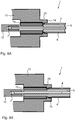
- FIG 1A shows a simplified sectional view of an electrical device 17 in which the connection of the invention 1 for receiving and contacting an RF conductor 4 is used.
- an electrical device 17 may be an RF filter that modifies an electrical signal.
- an RF filter depending on the design, for example, a resonator inner conductor 18, as in Figure 1A is shown.
- Such a resonator inner conductor 18 preferably extends from a housing bottom to a housing cover.
- Such resonator inner conductors 18 are not only capacitive, coupled as non-contact, but also depending on the application galvanic, or inductive.
- the signal to be coupled in or out is supplied via an electrical line, that is to say an HF conductor 4.
- Figure 1A shows how an RF conductor 4 can be connected to the resonator inner conductor 18 in a reproducible manner by means of the connection connection 1 according to the invention, quickly and simply and as far as its electrical properties are concerned.
- the HF conductor 4 consists in the simplest case of a simple wire, or a stranded wire. Dashed lines indicate that the RF conductor 4 may be surrounded by a dielectric 5. In the further embodiments, which are described in the later figures, it is at the RF conductor 4 to an inner conductor 4 of a coaxial cable.
- the resonator inner conductor 18 has a connection device 2, which comprises an HF conductor receiving element 10 with an HF conductor receiving bore 15.
- an RF conductor receiving bore 15 is introduced in the resonator inner conductor 18. In this case, this also represents the RF conductor receiving element 10. It may be that, for better electrical contacting, the HF conductor receiving bore 15 is galvanized together with the HF filter.
- connection connection 1 comprises an insert sleeve 7, which has a receiving opening 8 into which the HF conductor 4 can be introduced or inserted.
- connection connection 1 still has at least one solder deposit 9 for producing an electrically conductive connection.
- the at least one solder deposit 9 is in the embodiment of Figure 1A arranged on one end face of the insert sleeve 7.
- the at least one solder deposit 9 can be firmly pressed with the insert sleeve 7.
- the insert sleeve 7 may be inserted alone or together with the at least one solder deposit 9 in the RF conductor receiving bore 15 of the RF conductor receiving element 10.
- the outer diameter of the insert sleeve 7 is preferably selected such that the insert sleeve 7 frictionally or positively in the RF conductor receiving bore 15th is applied and only axially, ie in the direction of a insertion-side insertion opening 16 or against this insertion-side insertion opening 16 are moved.
- the insert sleeve 7 is preferably made of a plastic and is not deformable. This ensures that the distance of the RF conductor 4 to the RF conductor receiving element 10 for a plurality of connection connections 1, which are produced in a series, is constant.
- FIG. 1B shows a simplified sectional view of the electrical device 17 having an RF conductor receiving bore 15 into which the insert sleeve 7 is already used together with a solder deposit 9.
- the solder deposit 9 is in turn located on the end face of the insert sleeve 7, which is the insertion-side insertion opening 16 of the RF conductor receiving bore 15 closest.
- the at least one solder deposit 9 preferably does not protrude beyond the HF conductor receiving bore 15 after completion of the soldering operation, but terminates flush with its end. This preferably also applies before the melting of the at least one solder deposit 9.
- the HF conductor 4 can be easily inserted into the receiving opening 8 of the insert sleeve 7 in the next step.
- the arrangement of the at least one solder deposit 9 causes the RF conductor 4 is contacted only radially with the RF conductor receiving element 10.
- FIG. 2 shows a simplified sectional view of a connection connection 1 in the form of a connector 1, wherein the connection device 2 is designed as a connector 2.
- the RF conductor 4 is surrounded by the dielectric 5 and the outer conductor 6 and therefore represents an inner conductor 4 of a coaxial cable 3.
- connection device 1 in the form of the connector 1 also has the insert sleeve 7.
- This insert sleeve 7 has the receiving opening 8, which has a diameter which preferably corresponds to the diameter of the RF conductor 4 or is slightly larger.
- the receiving opening 8 is formed in the form of a blind hole and has a bottom.
- connection connection 1 likewise has at least one solder deposit 9 which serves to produce an electrically conductive connection between the HF conductor 4 of the coaxial cable 3 and an HF conductor receiving element 10 of the connection device 2.
- the solder deposit 9 has the shape of a partially open or closed ring made of a solid or elastic material.
- the solder deposit 9 is placed on the RF conductor 4 of the coaxial cable 3, so plugged and although preferably so far until the solder deposit 9 touches an end face 11 of the dielectric 5.
- the insert sleeve 7 is then also on the HF conductor 4 is placed until it is in contact with the solder deposit 9.
- the solder deposit 9 is therefore arranged between the insert sleeve 7 and the end face 11 of the dielectric 5 of the male or female coaxial cable 3.
- the solder deposit 9 can be fixed to the HF conductor 4, for example by crimping. Slipping along the RF conductor 4 is then no longer possible.
- the HF conductor 4 may also have small projections or indentations on which the at least one solder deposit is secured against slipping.
- the insert sleeve 7 is preferably a hollow cylinder. In order to achieve the lowest possible heat capacity, the insert sleeve 7 is preferably made of a plastic. The insert sleeve 7 can be produced for example in an injection molding process. By contrast, the RF conductor receiving element 10 is made of a metal.
- connection device 2 in the form of a connector 2 also has an outer conductor socket 12 which serves to receive the coaxial cable 3.
- the outer conductor bushing 12 has for this purpose a cable receiving opening 13.
- the outer conductor socket 12 is preferably formed from or coated with a conductive material and has an outer conductor contacting portion 14, with which an electrically conductive contact with the outer conductor 6 of the male coaxial cable 3 is produced becomes.
- the cable receiving opening 13 has a diameter which preferably corresponds to the diameter of the coaxial cable 3 to its outer conductor 6.
- An outer protective sheath of the coaxial cable 3 is preferably stripped in the region of the cable receiving opening 13.
- the HF conductor receiving element 10 has an HF conductor receiving bore 15.
- the HF conductor receiving bore 15 serves to receive the HF conductor 4 of the coaxial cable 3, wherein the HF conductor receiving element 10 is preferably centered within the outer conductor socket 12.
- the diameter of the RF conductor receiving bore 15 is selected such that it corresponds to the outer diameter of the insert sleeve 7 or is slightly larger.
- the insert sleeve 7 can be inserted via an insertion-side insertion opening 16 in the RF conductor receiving bore 15 of the RF conductor receiving element 10.
- the diameter of the RF conductor receiving bore 15 is preferably constant. It changes, in particular it does not preferably increase over its axial length.
- FIG. 3 shows a simplified sectional view of the terminal connection 1 according to the invention in the form of the connector 1, which is caused by an insertion of the coaxial cable 3 together with the insert sleeve 7 and the solder deposit 9 in the RF conductor receiving element 10 of the connection device 2.
- the insert sleeve 7 is arranged within the RF conductor receiving bore 15, so within the RF conductor receiving element 10 stop limited.
- An end face of the RF conductor receiving element 10 protrudes beyond an end face of the insert sleeve 7 so far that the at least one solder deposit 9 is arranged on the end face of the insert sleeve 7 and preferably ends flush with the end face of the RF conductor receiving element 10.
- the at least one solder deposit 9 can also project beyond the front side of the HF conductor receiving element 10. However, after completion of the soldering operation, it should lie flush against the end face of the HF conductor receiving element 10 or not project beyond it. A part of the end face 11 of the dielectric 5 of the male or female coaxial cable 3 is supported in the embodiment according to FIG FIG. 3 on the front side of the RF conductor receiving element 10 from.
- the RF conductor 4 of the coaxial cable 3 extends in the receiving opening 8 of the insert sleeve 7 only over part of the length of the receiving opening 8, that is, only over a part of the length of the insert sleeve 7. However, it would also be possible for the RF conductor 4 of the coaxial cable 3 extends over the entire length of the receiving opening 8 or even slightly beyond it.
- At least one solder deposit 9 already melted.
- the at least one solder deposit 9 can be heated, for example, by means of an induction loop.
- the HF conductor 4 of the accommodated coaxial cable 3 is already connected in an electrically conductive manner to the HF conductor receiving element 10.
- the outer conductor contacting section 14 of the outer conductor bush 12 with the outer conductor 6 of the accommodated coaxial cable 3 becomes electrically conductive connected. This can be done for example by pressing and / or crimping. Preferably, the electrical contact between the outer conductor 6 and the réelleleiter gleich istsabites 14 is separated from an additional, preferably purely mechanical fixation.
- the outer conductor 6 of the coaxial cable 3 is in this case on a support shoulder 20.
- a further dielectric to be arranged between an end face of the outer conductor 6 of the coaxial cable 3 and the support shoulder 20 of the outer conductor socket 12, so that electrical contact between the end face of the outer conductor 6 of the coaxial cable 3 and the support shoulder 20 of the outer conductor socket 12 is prevented. It is precisely such front-side contacts that pose problems in terms of reproducibility of the electrical contact. It is therefore advantageous if the outer conductor 6 is electrically contacted solely with a radial component.
- FIG. 4A shows a further simplified sectional view of the connection device 2, in the RF conductor receiving element 10, the insert sleeve 7 is already used.
- the insert sleeve 7 is not placed on the RF conductor 4 of the coaxial cable 3, but is inserted directly into the RF conductor receiving bore 15 of the RF conductor receiving element 10 of the connection device 2.
- Connection device 2 can subsequently be inserted into the space 30 of RF conductor receiving bore 15 remaining towards insertion opening 16, at least one solder deposit 9, which is preferably an annular solder deposit 9.
- At least one solder deposit 9 which is preferably an annular solder deposit 9.
- An end face of the at least one solder deposit 9 preferably terminates flush with the end face of the HF conductor receiving element 10. It is also possible that the end face of the RF conductor receiving element 10 projects slightly beyond an end face of the at least one solder depot 9, or vice versa, that the end face of the at least one solder depot 9 projects beyond the end face of the RF conductor receiving element 10.
- the RF conductor 4 of the male coaxial cable 3 can be guided both through the solder deposit 9 and through the receiving opening 8 of the insert sleeve 7.
- FIG. 5A shows a longitudinal section through a further embodiment of the insert sleeve 7.
- the solder deposit 9 is preferably not arranged in such insert sleeve 7 between the insert sleeve 7 and the end face 11 of the dielectric 5 of the male coaxial cable 3, but in the insert sleeve 7 itself at least one receiving channel 40, which in particular has the shape of a bore.
- the receiving channel 40 preferably extends radially from outside to inside the receiving opening 8.
- the receiving channel 40 serves to receive the at least one solder depot 9.
- the receiving channel 40 may have a constant diameter. However, it can also be made variable in its diameter. For example, can a longitudinal section through the receiving channel 40 have a conical shape.
- the solder deposit 9, which in this case preferably has a viscous consistency, is introduced into the at least one receiving channel 40. Subsequently, the insert sleeve 7 can be placed on the RF conductor 4 of the coaxial cable 3 and used with this directly in the RF conductor receiving bore 15. It is also possible that the at least one receiving channel 40 is filled with the solder deposit 9 only when the insert sleeve 7 is placed on the RF conductor 4 of the coaxial cable 3. In this case, it is ensured that only non-aged solder is used to produce the solder deposit 9.
- the solder deposit 9 can also be preferably introduced on half the length of the insert sleeve 7 in this. In the case of several solder deposits 9, these are preferably arranged symmetrically with respect to an imaginary straight line which runs transversely through the longitudinal section through the center of the insert sleeve 7. This ensures that the solder deposits 9 always contact the RF conductor 4 at the same location with the RF conductor receiving element 10, regardless of the direction in which the insert sleeve 7 is inserted into the RF conductor receiving bore 15.
- the insert sleeve 7 off FIG. 5A also has a beveled section 42 in longitudinal section.
- This section 42 facilitates the insertion of the insert sleeve 7 in the RF conductor receiving bore 15.
- the insert sleeve 7 is therefore preferably formed conically at its insertion end in longitudinal section.
- the bevel can in Longitudinal section, however, also parabolic.
- the insert sleeve 7 may also have at both ends about such a chamfer 42. In this case, it does not matter in which direction the insert sleeve 7 is placed on the RF conductor 4 or in the RF conductor receiving bore 15, or used.
- the insert sleeve 7 has on its circumference at least one section 41 protruding counter to the direction of insertion into the HF conductor receiving element 10, which can be referred to as a barb 41.
- This protruding portion 41 can also be guided around the circumference of the insert sleeve 7 radially, thus extending without interruption on the circumference.
- the protruding portion 41 is preferably elastic, so that it conforms to the circumference of the insert sleeve 7 when inserted into the RF conductor receiving bore 15 and only in the case in which the insert sleeve 7 arrives at the desired position within the RF conductor receiving bore 15 is engaged in a corresponding groove or crack.
- the insert sleeve 7 has at least one coding element on its circumference, as a result of which the insert sleeve 7 can be inserted only at a specific position into the HF conductor receiving element 10, that is to say into the RF conductor receiving bore 15 and is mounted so as to be secure against rotation within this limit stop is.
- FIG. 5C shows a longitudinal section through a further embodiment of the insert sleeve 7, which has various receiving channels 40 which are spaced apart in the longitudinal direction within the insert sleeve 7.
- the longitudinal direction is the Z-axis
- the individual receiving channels 40 have the same dimensions and the same position with regard to an imaginary X / Y coordinate system, but with regard to their position in the Z axis differ from each other.
- the individual receiving channels 40 would be "congruent” arranged one above the other.
- the individual receiving channels 40 are arranged "offset" one above the other.
- the at least two receiving channels 40 are spaced apart in the longitudinal direction and in plan view congruent, partially congruent or completely offset from one another are arranged one above the other.
- the receiving channels 40 are in the FIGS. 5A to 5C already filled with a solder deposit 9.
- FIG. 5D shows a cross section through the insert sleeve 7, which has four receiving channels 40 for receiving a respective Lotdepots 9.
- the receiving channels 40 are preferably formed in the form of a bore, which in the embodiment of FIG. 5D extend radially from outside to inside the receiving opening 8.
- the insert sleeve 7 preferably has X receiving channels 40, wherein X is preferably ⁇ 2.
- There are four receiving channels 40. This means that each receiving channel 40 is offset from the other receiving channel by ⁇ 90 °.
- FIG. 5E shows a cross section through the insert sleeve 7, wherein the receiving channel 40 has the shape of a cutout.
- This section comprises, in plan view of the cross section through the insert sleeve 7, a range of more than 180 °, preferably more than 220 °, more preferably more than 260 °, more preferably more than 300 °, further preferably more than 340 ° but less than 350 °.
- the cut-out covers a range of 270 °.
- the solder deposit 9 in this case preferably has the form of an open ring which can be "clipped" or "inserted” into the cutout.
- the thickness of the cutout corresponds approximately to the diameter of the receiving channels 40 from the FIGS. 5A to 5D ,
- the diameter of each receiving channel 40 may be greater than the length of the corresponding receiving channel 40. However, it may also be that the length of a receiving channel 40 is greater than the diameter of the receiving channel.
- FIG. 6 shows a simplified sectional view of another embodiment of the connection connection 1 according to the invention in the form of a connector 1, wherein the insert sleeve 7 is disposed between the solder depot 9 and the dielectric 5 of the coaxial cable 3.
- the solder deposit 9 is inserted in front of the insert sleeve 7 in the RF conductor receiving bore 15 of the RF conductor receiving element 10.
- the insert sleeve 7 and then or at the same time the solder deposit 9 plugged onto the RF conductor 4 of the coaxial cable 3.
- the RF conductor 4 it is also possible for the RF conductor 4 to extend through the solder deposit 9, ending within this. In this case, the RF conductor 4 does not touch the HF conductor receiving element 10 with its front side. An electrical contact between the RF conductor 4 and the RF conductor receiving element 10 takes place in contrast to the previous embodiments, which show a predominant radial contact, also the front side.
- FIG. 6 Within FIG. 6 is the dielectric 5 of the coaxial cable 3 on an end face of the RF conductor receiving element 10.
- the outer conductor 6 rests with its end face against the support shoulder 20 of the outer conductor bushing 12.
- FIG. 7 shows a simplified sectional view of another embodiment of the connection connection 1 according to the invention in the form of a connector 1.
- An insert sleeve 7 is not used.
- the dielectric 5 of the coaxial cable 3 is inserted directly into the RF conductor receiving bore 15 together with the above RF conductor 4.
- the solder deposit 9 can first be inserted into the HF conductor receiving bore 15, with the HF conductor 4 and the dielectric 5 of the male coaxial cable 3 subsequently being introduced into the HF conductor receiving bore 15.
- a placement of the solder depot 9 on the RF conductor 4 is also possible, both of which are subsequently introduced into the RF conductor receiving bore 15.
- the solder deposit 9 preferably has the form of a partially open or closed ring.
- the outer diameter of the preferably annular Lotdepots 9 is preferably equal to the outer diameter of the dielectric 5. It may also be possible that the part of the dielectric 5, which is inserted into the RF conductor receiving bore 15 has a smaller outer diameter than the part of the Dielectric 5, which is still surrounded by the outer conductor 6.
- FIGS. 6 and 7 allow a soldering of the RF conductor 4 at its front without mechanical stresses to damage them.
- Figure 8A shows a simplified sectional view of another embodiment of the terminal connection 1 according to the invention in the form of a connector 1, wherein at least one matching element 70 is disposed within the connection device 2 to adjust the characteristic impedance of the coaxial cable 3. Due to the reproducibility of the RF conductor soldering inter alia by means of the insert sleeve 7 and "long connector" can be produced inexpensively.
- the RF conductor 4 such a connector 1 is preferably made of beryllium copper.
- connection device 2 Due to the great length of the connection device 2 in the form of a connector 2, the distance between the electrical contact of the RF conductor 4 with the RF conductor receiving element 10 to the Jardinleiter gleich istsabites 14, where the outer conductor 4 is electrically connected to the outer conductor socket 12, large , This may cause problems with the adjustment (VSWR, Voltage Standing Wave Ratio). arise. This is compensated by a suitable dielectric, which is the matching element 70.
- the at least one matching element 70 is arranged between the outer conductor contacting section 14 and the HF conductor receiving element 10. It preferably has the shape of a hollow cylinder, wherein the RF conductor 4 of the coaxial cable 3 is guided therethrough.
- the matching element 70 preferably surrounds the RF conductor 4 radially. However, it is also possible that the at least one matching element 70 surrounds the RF conductor 4 not on its entire circumference, ie in the range of 360 °, but only in a certain section.
- FIG. 8B shows a simplified sectional view of another embodiment of the connection connection 1 according to the invention in the form of a connector 1, wherein the at least one matching element 70 within the connection device 2, which has the shape of a connector 2 is arranged to adjust the characteristic impedance of the coaxial cable 3.
- the matching element 70 also surrounds the dielectric 5 of the coaxial cable 3.
- the outer radius of the dielectric 5 changes within FIG. 8B ,
- the region of the dielectric 5 which is surrounded by the matching element 70 has a smaller outer diameter than the region of the dielectric 5 on which the outer conductor 6 rests.
- the outer diameter of the dielectric 5 preferably changes in the region of the support shoulder 20.
- the adaptation element 70 can be used, for example, prior to the assembly of the connection device 2 or, alternatively, be introduced via the cable receiving opening 13. In the latter case, however, the outer conductor bush 12 has no support shoulder 20.
- FIGS 9A and 9B show a simplified sectional view of another embodiment of the connection connection 1 according to the invention in the form of an electrical device 17, wherein the cross section of the RF conductor 4 is square.
- FIG. 9B shows a cross section along the line BB 'from Figure 9A .
- the male or female RF conductor 4 may also have a cross-section that corresponds or approximates in plan view a square, a rectangle, an oval, a circle, or a regular or irregular n-polygon.
- the cross section of the receiving opening 8 of the insert sleeve 7 is preferably adapted to the cross section of the RF conductor 4. This prevents twisting of the RF conductor 4 in the insert sleeve 7, whereby the solder connection is not damaged.
- Figure 10A shows a simplified sectional view of the electrical device 17, in which the connection connection 1 of the invention for receiving and contacting the RF conductor 4 is used, wherein the RF conductor 4 is partially surrounded by a dielectric 5 and an outer conductor 6 and thereby the inner conductor. 4 of the coaxial cable 3 represents.
- the electrical device 17 is, for example, an HF filter.
- the RF filter points as in FIGS. 1A and 1B a resonator inner conductor 18.
- Within Figure 10A is still a housing wall 50 shown.
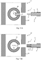
- the resonator inner conductor 18 has a circular recess 51, which preferably extends in the direction of a housing cover, not shown.
- the RF conductor receiving bore 15 is in contrast to that of FIGS.
- the RF conductor 4 is also surrounded by a dielectric 5 and an outer conductor 6.
- the RF conductor 4 and the dielectric 5 protrude through the housing wall 50 into the RF filter.
- the outer conductor 6 ends in the middle of the housing wall 50 and is at least with its end face in electrical contact therewith. It is also possible that the outer conductor 6 is additionally in electrical contact with the housing wall 50 with a part of its so,swandung.
- the dielectric 5 lies with its end face against the solder deposit 9.
- FIG. 10B shows, as well Figure 10A a simplified sectional view of the electrical device 17.
- the outer conductor 6 of the coaxial cable 3 does not end within the housing wall 50. Therefore, only the RF conductor 4 and the dielectric 5 are guided through the bore, which runs through the housing wall 50.
- the outer conductor 6 rests with its end face against the outer surface of the housing wall 50.
- the bore through the housing wall 50 has a diameter corresponding to the outer diameter of the dielectric 5, or is slightly larger. The diameter is smaller, however, than the diameter of the outer conductor. 6
- the Figures 11A and 11B show a simplified sectional view of the electrical device 17, in which the terminal connection 1 according to the invention for receiving and contacting the RF conductor 4 is used, wherein the RF conductor 4 is partially surrounded by a dielectric 5 and an outer conductor 6 and thereby the inner conductor. 4 a coaxial cable 3 represents.
- the RF conductor 4 protrudes beyond the surrounding dielectric 5.
- the dielectric 5 also projects beyond the outer conductor 6, which surrounds it.
- the insert sleeve 7 is already used together with the solder deposit 9 in the RF conductor receiving bore 15 of the RF conductor receiving element 10.
- the insert sleeve 7 is placed together with the at least one solder deposit 9 on the RF conductor 4 of the coaxial cable 3.
- the coaxial cable 3 is therefore at least partially inserted together with the insert sleeve 7 and the at least one solder deposit 9 through the opening in the housing wall 50 in the RF conductor receiving bore 15 of the RF conductor receiving element 10.
- FIG. 12 shows a flow chart, which illustrates the production of the connection connection 1 according to the invention in the form of a connector 1 in more detail.
- the male RF conductor 4 must be prepared accordingly. This can be done through different steps. It is possible, for example, a successive or simultaneous placement of a preferably annular Lotdepots 9 and the insert sleeve 7 on the RF conductor 4. The preferably annular Lotdepot 9 is then located between the end face of the insert sleeve 7 and the end face 11 of the dielectric 5 of the coaxial cable 3. Im In contrast thereto, sequential or simultaneous placement of the insert sleeve 7 and the preferably annular solder depot 9 on the HF conductor 4. The solder depot 9 is therefore arranged at the end of the HF conductor 4. The HF conductor 4 extends through the insert sleeve 7 and ends within the solder deposit 9.
- the insert sleeve 7 is placed on the RF conductor 4, wherein the at least one solder deposit 9 already arranged on or in the insert sleeve 7 is.
- the insert sleeve 7 could, for example, have receiving channels 40.
- the insert sleeve 7 it would also be possible for the insert sleeve 7 to be placed on the HF conductor 4 and for at least one solder deposit 9 to be arranged thereafter in the insert sleeve 7. Subsequently, the male RF conductor 4 can be introduced together with the insert sleeve 7 and the at least one solder deposit 9 in the RF conductor receiving element 10, ie in the RF conductor receiving bore 15 of the connection device 2.
- method step S 2 could also be carried out.
- the connection device 2 is instead prepared accordingly. This succeeds, for example in that the at least one solder deposit 9 is arranged in the insert sleeve 7, and that subsequently the insert sleeve 7 with the at least one solder deposit 9 is introduced into the HF conductor receiving bore 15 of the HF conductor receiving element 10 of the connection device 2.
- the insert sleeve 7 is inserted into the HF conductor receiving bore 15 of the RF conductor receiving element 10 of the connection device 2, and that subsequently a preferably annular solder depot 9 in the remaining to the HF conductor receiving bore 15 back space 30 of the HF Conductor receiving bore 15 of the RF conductor receiving element 10 of the connection device 2 is introduced. It would also be possible for the preferably annular solder deposit 9 to be introduced into the HF conductor receiving bore 15 of the HF conductor receiving element 10 of the connecting device 2 and furthermore for the insert sleeve 7 to be inserted or introduced into the HF conductor receiving bore 15 of the RF conductor receiving element 10 of the connecting device 2 becomes. Furthermore, the RF conductor 4 of the male coaxial cable 3 would have to be inserted into the receiving opening 8 of the insert sleeve 7 or into the receiving opening 8 of the insert sleeve 7 and into the annular solder deposit 9.
- the method step S 3 could also be carried out.
- both the RF conductor 4 and the connection device 2 are prepared.
- the Eisatzhülse 7 is inserted into the RF conductor receiving bore 15 of the RF conductor receiving element 10 of the connecting device 2 and at the same time or alternately to the preferably annular solder deposit 9th placed on the RF conductor 4.
- the RF conductor 4 is inserted into the receiving opening 8 of the insert sleeve 7.
- the method step S 4 is carried out.
- the solder deposit 9 is heated until it is molten and thus the RF conductor 4 electrically conductively connects to the RF conductor receiving element 10.
- an induction loop can be used, which melts the solder deposit 9.
- the RF conductor 4 In the event that the RF conductor 4 is still surrounded by a dielectric 5 and optionally also by an outer conductor 6, ie it represents the inner conductor 4 of a coaxial cable, must for the first or second or third process step S 1 , S 2 or S 3 nor the method step S 0 are executed. In this method step S 0 , the RF conductor 4 of the male coaxial cable 3 is exposed. This is best done by appropriate stripping tools. The RF conductor 4 therefore protrudes beyond the dielectric 5 and the optional outer conductor 6.
- the outer conductor contacting section 14 of the outer conductor socket 12 can be pressed and / or crimped with the outer conductor 6 of the accommodated coaxial cable 3, so that electrical contact is also established between the outer conductor 6 of the coaxial cable 3 and the outer conductor socket 12.
- the insert sleeve 7 has at least one receiving channel 40 or the like, in which the solder deposit 9 is arranged.
Landscapes
- Engineering & Computer Science (AREA)
- Manufacturing & Machinery (AREA)
- Physics & Mathematics (AREA)
- Electromagnetism (AREA)
- Coupling Device And Connection With Printed Circuit (AREA)
- Manufacturing Of Electrical Connectors (AREA)
- Multi-Conductor Connections (AREA)
Applications Claiming Priority (1)
| Application Number | Priority Date | Filing Date | Title |
|---|---|---|---|
| DE102015006070.8A DE102015006070B3 (de) | 2015-05-07 | 2015-05-07 | Anschlussverbindung mit einem HF-Leiter, insbesondere für ein Koaxialkabel und Verfahren zur Herstellung dieser Anschlussverbindung |
Publications (3)
| Publication Number | Publication Date |
|---|---|
| EP3091613A2 true EP3091613A2 (fr) | 2016-11-09 |
| EP3091613A3 EP3091613A3 (fr) | 2017-03-29 |
| EP3091613B1 EP3091613B1 (fr) | 2018-05-09 |
Family
ID=55661339
Family Applications (1)
| Application Number | Title | Priority Date | Filing Date |
|---|---|---|---|
| EP16163895.2A Active EP3091613B1 (fr) | 2015-05-07 | 2016-04-05 | Dispositif de raccordement pour un conducteur hf, en particulier pour un câble coaxial et procédé de fabrication dudit dispositif de raccordement |
Country Status (6)
| Country | Link |
|---|---|
| US (1) | US9780430B2 (fr) |
| EP (1) | EP3091613B1 (fr) |
| KR (1) | KR101697721B1 (fr) |
| CN (1) | CN106129655B (fr) |
| DE (1) | DE102015006070B3 (fr) |
| MX (1) | MX353533B (fr) |
Families Citing this family (6)
| Publication number | Priority date | Publication date | Assignee | Title |
|---|---|---|---|---|
| KR101848259B1 (ko) | 2016-09-09 | 2018-04-16 | 주식회사 이너트론 | 공진기 및 이를 포함하는 필터 |
| US10708979B2 (en) | 2016-10-07 | 2020-07-07 | De-Ice Technologies | Heating a bulk medium |
| CN106785244B (zh) * | 2016-12-20 | 2020-11-27 | 中国航空工业集团公司雷华电子技术研究所 | 一种微波连接器连接结构 |
| DE102018212789A1 (de) * | 2018-07-31 | 2020-02-06 | Astyx Gmbh | Vorrichtung Verbindungsstruktur zwischen Auswerteelektronik und Sonde in Zylindersystemen |
| EP4223643A1 (fr) * | 2018-08-27 | 2023-08-09 | De-Ice Technologies, Inc. | Systèmes de dégivrage |
| CN212991534U (zh) * | 2020-10-16 | 2021-04-16 | 张家港友诚新能源科技股份有限公司 | 一种电源芯线的液冷装置 |
Citations (4)
| Publication number | Priority date | Publication date | Assignee | Title |
|---|---|---|---|---|
| DE69307329T2 (de) | 1992-09-14 | 1997-08-21 | Raychem Sa Nv | Anschlussvorrichtung und verfahren |
| US20100144200A1 (en) | 2004-08-27 | 2010-06-10 | Holliday Randall A | Universal cable connector with interchangeable color bands |
| DE10251905C5 (de) | 2001-11-17 | 2012-06-14 | Spinner Gmbh | Lötbarer koaxialer Steckverbinder |
| WO2015000749A1 (fr) | 2013-07-04 | 2015-01-08 | Huber+Suhner Ag | Connecteur pour câble coaxial haute fréquence |
Family Cites Families (8)
| Publication number | Priority date | Publication date | Assignee | Title |
|---|---|---|---|---|
| US4487999A (en) * | 1983-01-10 | 1984-12-11 | Isotronics, Inc. | Microwave chip carrier |
| DE3715594C2 (de) * | 1987-05-09 | 1994-07-14 | Broadcast Television Syst | Anordnung zum Anschluß von Ausgangs- und Eingangsstufen einer Sende/Empfangseinrichtung |
| US5046966A (en) * | 1990-10-05 | 1991-09-10 | International Business Machines Corporation | Coaxial cable connector assembly |
| US6118353A (en) * | 1999-02-17 | 2000-09-12 | Hughes Electronics Corporation | Microwave power divider/combiner having compact structure and flat coupling |
| ATE542272T1 (de) * | 2004-02-05 | 2012-02-15 | Tyco Electronics Belgium Ec Bv | Verbinder für koaxialkabel |
| CN100546122C (zh) | 2004-08-03 | 2009-09-30 | 泰科电子Amp有限责任公司 | 电气插头和配合该插头的方法 |
| DE102012110217B4 (de) * | 2012-10-25 | 2016-03-24 | Ims Connector Systems Gmbh | Koaxialkabelbuchse mit Lotdepot und Verfahren zur Herstellung |
| DE102013100438B3 (de) * | 2013-01-16 | 2014-07-17 | Telegärtner Karl Gärtner GmbH | Koaxialkabelverbinder mit Lotdepot |
-
2015
- 2015-05-07 DE DE102015006070.8A patent/DE102015006070B3/de not_active Expired - Fee Related
-
2016
- 2016-04-05 EP EP16163895.2A patent/EP3091613B1/fr active Active
- 2016-05-04 MX MX2016005842A patent/MX353533B/es active IP Right Grant
- 2016-05-04 KR KR1020160055251A patent/KR101697721B1/ko active IP Right Grant
- 2016-05-06 CN CN201610298054.XA patent/CN106129655B/zh active Active
- 2016-05-06 US US15/148,335 patent/US9780430B2/en active Active
Patent Citations (4)
| Publication number | Priority date | Publication date | Assignee | Title |
|---|---|---|---|---|
| DE69307329T2 (de) | 1992-09-14 | 1997-08-21 | Raychem Sa Nv | Anschlussvorrichtung und verfahren |
| DE10251905C5 (de) | 2001-11-17 | 2012-06-14 | Spinner Gmbh | Lötbarer koaxialer Steckverbinder |
| US20100144200A1 (en) | 2004-08-27 | 2010-06-10 | Holliday Randall A | Universal cable connector with interchangeable color bands |
| WO2015000749A1 (fr) | 2013-07-04 | 2015-01-08 | Huber+Suhner Ag | Connecteur pour câble coaxial haute fréquence |
Also Published As
| Publication number | Publication date |
|---|---|
| KR101697721B1 (ko) | 2017-01-18 |
| US20160329619A1 (en) | 2016-11-10 |
| EP3091613A3 (fr) | 2017-03-29 |
| DE102015006070B3 (de) | 2016-06-23 |
| US9780430B2 (en) | 2017-10-03 |
| MX2016005842A (es) | 2016-11-07 |
| CN106129655A (zh) | 2016-11-16 |
| MX353533B (es) | 2018-01-18 |
| KR20160131930A (ko) | 2016-11-16 |
| CN106129655B (zh) | 2018-04-10 |
| EP3091613B1 (fr) | 2018-05-09 |
Similar Documents
| Publication | Publication Date | Title |
|---|---|---|
| EP3091613B1 (fr) | Dispositif de raccordement pour un conducteur hf, en particulier pour un câble coaxial et procédé de fabrication dudit dispositif de raccordement | |
| EP3251180B1 (fr) | Ensemble connecteur enfichable à manchon compensateur | |
| EP3251174B1 (fr) | Ensemble connecteur avec sertissage de compensation | |
| DE3505189C2 (de) | Steckverbinder für Koaxialkabel | |
| WO2016120006A1 (fr) | Dispositif connecteur avec partie formant manchon | |
| EP3396793A1 (fr) | Corps de contact pour connecteur à fiche | |
| DE102014109720A1 (de) | Elektrische Heizvorrichtung mit Steckkontakt | |
| EP2456013B1 (fr) | Connexion par sertissage à complémentarité de forme et de force pour un connecteur à fiche coaxial et outil de sertissage associé | |
| EP3387710A1 (fr) | Agencement de conducteur extérieur pour fiche coaxiale | |
| EP3361826A1 (fr) | Cartouche de chauffage | |
| EP0470924B1 (fr) | Raccordement à fiche pour des câbles | |
| EP2725659B1 (fr) | Manchon de câble coaxial | |
| EP3837741B1 (fr) | Ensemble de câble | |
| EP3364507A1 (fr) | Connecteur électrique pour un câble électrique multi-fils | |
| DE102010052627A1 (de) | Mantelleitungscrimpverbindung für Zug- und Druckentlastung einschließlich Schirmübertragung zur Metallhülse | |
| DE19528235C2 (de) | Vorrichtung zur Verbindung der Abschirmung eines Kabels mit dem Gehäuse eines elektrischen Verbinders | |
| EP3140883B1 (fr) | Élément de contact | |
| DE102021112505A1 (de) | Crimpkontakt, Crimpverbindung und Verfahren zur Herstellung einer Crimpverbindung | |
| DE102015003579A1 (de) | HF-Steckverbinder zur lotfreien Kontaktierung eines Koaxialkabels | |
| DE102011077886B4 (de) | Verfahren zur Leitungskonfektionierung | |
| EP2993737B1 (fr) | Dispositif de connexion a fiches haute frequence, en particulier dispositif de connexion coaxial pour des prises d'antenne | |
| DE102006049966A1 (de) | Aufdopplung im Crimpbereich eines Steckers oder eines Kupplers | |
| EP4092844A1 (fr) | Connecteur enfichable électrique et procédé de montage d'un agencement de connecteur enfichable électrique | |
| WO2024068558A1 (fr) | Élément de contact hybride | |
| EP3382825A1 (fr) | Étanchéification lors du moulage par injection sur un assemblage par soudure entre des contacts de douille et un grillage estampé |
Legal Events
| Date | Code | Title | Description |
|---|---|---|---|
| PUAI | Public reference made under article 153(3) epc to a published international application that has entered the european phase |
Free format text: ORIGINAL CODE: 0009012 |
|
| AK | Designated contracting states |
Kind code of ref document: A2 Designated state(s): AL AT BE BG CH CY CZ DE DK EE ES FI FR GB GR HR HU IE IS IT LI LT LU LV MC MK MT NL NO PL PT RO RS SE SI SK SM TR |
|
| AX | Request for extension of the european patent |
Extension state: BA ME |
|
| PUAL | Search report despatched |
Free format text: ORIGINAL CODE: 0009013 |
|
| AK | Designated contracting states |
Kind code of ref document: A3 Designated state(s): AL AT BE BG CH CY CZ DE DK EE ES FI FR GB GR HR HU IE IS IT LI LT LU LV MC MK MT NL NO PL PT RO RS SE SI SK SM TR |
|
| AX | Request for extension of the european patent |
Extension state: BA ME |
|
| RIC1 | Information provided on ipc code assigned before grant |
Ipc: H01R 4/02 20060101AFI20170220BHEP Ipc: H01R 24/40 20110101ALN20170220BHEP Ipc: H01R 9/05 20060101ALN20170220BHEP |
|
| STAA | Information on the status of an ep patent application or granted ep patent |
Free format text: STATUS: REQUEST FOR EXAMINATION WAS MADE |
|
| 17P | Request for examination filed |
Effective date: 20170725 |
|
| RBV | Designated contracting states (corrected) |
Designated state(s): AL AT BE BG CH CY CZ DE DK EE ES FI FR GB GR HR HU IE IS IT LI LT LU LV MC MK MT NL NO PL PT RO RS SE SI SK SM TR |
|
| GRAP | Despatch of communication of intention to grant a patent |
Free format text: ORIGINAL CODE: EPIDOSNIGR1 |
|
| STAA | Information on the status of an ep patent application or granted ep patent |
Free format text: STATUS: GRANT OF PATENT IS INTENDED |
|
| RIC1 | Information provided on ipc code assigned before grant |
Ipc: H01R 24/40 20110101ALN20171204BHEP Ipc: H01R 9/05 20060101ALN20171204BHEP Ipc: H01R 4/02 20060101AFI20171204BHEP |
|
| INTG | Intention to grant announced |
Effective date: 20171220 |
|
| GRAS | Grant fee paid |
Free format text: ORIGINAL CODE: EPIDOSNIGR3 |
|
| GRAA | (expected) grant |
Free format text: ORIGINAL CODE: 0009210 |
|
| STAA | Information on the status of an ep patent application or granted ep patent |
Free format text: STATUS: THE PATENT HAS BEEN GRANTED |
|
| AK | Designated contracting states |
Kind code of ref document: B1 Designated state(s): AL AT BE BG CH CY CZ DE DK EE ES FI FR GB GR HR HU IE IS IT LI LT LU LV MC MK MT NL NO PL PT RO RS SE SI SK SM TR |
|
| REG | Reference to a national code |
Ref country code: GB Ref legal event code: FG4D Free format text: NOT ENGLISH |
|
| REG | Reference to a national code |
Ref country code: CH Ref legal event code: EP Ref country code: AT Ref legal event code: REF Ref document number: 998353 Country of ref document: AT Kind code of ref document: T Effective date: 20180515 |
|
| REG | Reference to a national code |
Ref country code: IE Ref legal event code: FG4D Free format text: LANGUAGE OF EP DOCUMENT: GERMAN |
|
| REG | Reference to a national code |
Ref country code: DE Ref legal event code: R096 Ref document number: 502016001010 Country of ref document: DE |
|
| REG | Reference to a national code |
Ref country code: DE Ref legal event code: R082 Ref document number: 502016001010 Country of ref document: DE Representative=s name: FLACH BAUER & PARTNER PATENTANWAELTE MBB, DE Ref country code: DE Ref legal event code: R082 Ref document number: 502016001010 Country of ref document: DE Representative=s name: FLACH BAUER STAHL PATENTANWAELTE PARTNERSCHAFT, DE |
|
| REG | Reference to a national code |
Ref country code: SE Ref legal event code: TRGR |
|
| REG | Reference to a national code |
Ref country code: NL Ref legal event code: MP Effective date: 20180509 |
|
| REG | Reference to a national code |
Ref country code: DE Ref legal event code: R081 Ref document number: 502016001010 Country of ref document: DE Owner name: ERICSSON AB, SE Free format text: FORMER OWNER: KATHREIN-WERKE KG, 83022 ROSENHEIM, DE Ref country code: DE Ref legal event code: R081 Ref document number: 502016001010 Country of ref document: DE Owner name: TELEFONAKTIEBOLAGET LM ERICSSON (PUBL), SE Free format text: FORMER OWNER: KATHREIN-WERKE KG, 83022 ROSENHEIM, DE Ref country code: LT Ref legal event code: MG4D Ref country code: DE Ref legal event code: R082 Ref document number: 502016001010 Country of ref document: DE Representative=s name: FLACH BAUER STAHL PATENTANWAELTE PARTNERSCHAFT, DE Ref country code: DE Ref legal event code: R081 Ref document number: 502016001010 Country of ref document: DE Owner name: KATHREIN SE, DE Free format text: FORMER OWNER: KATHREIN-WERKE KG, 83022 ROSENHEIM, DE |
|
| PG25 | Lapsed in a contracting state [announced via postgrant information from national office to epo] |
Ref country code: NO Free format text: LAPSE BECAUSE OF FAILURE TO SUBMIT A TRANSLATION OF THE DESCRIPTION OR TO PAY THE FEE WITHIN THE PRESCRIBED TIME-LIMIT Effective date: 20180809 Ref country code: ES Free format text: LAPSE BECAUSE OF FAILURE TO SUBMIT A TRANSLATION OF THE DESCRIPTION OR TO PAY THE FEE WITHIN THE PRESCRIBED TIME-LIMIT Effective date: 20180509 Ref country code: LT Free format text: LAPSE BECAUSE OF FAILURE TO SUBMIT A TRANSLATION OF THE DESCRIPTION OR TO PAY THE FEE WITHIN THE PRESCRIBED TIME-LIMIT Effective date: 20180509 Ref country code: BG Free format text: LAPSE BECAUSE OF FAILURE TO SUBMIT A TRANSLATION OF THE DESCRIPTION OR TO PAY THE FEE WITHIN THE PRESCRIBED TIME-LIMIT Effective date: 20180809 |
|
| PG25 | Lapsed in a contracting state [announced via postgrant information from national office to epo] |
Ref country code: LV Free format text: LAPSE BECAUSE OF FAILURE TO SUBMIT A TRANSLATION OF THE DESCRIPTION OR TO PAY THE FEE WITHIN THE PRESCRIBED TIME-LIMIT Effective date: 20180509 Ref country code: RS Free format text: LAPSE BECAUSE OF FAILURE TO SUBMIT A TRANSLATION OF THE DESCRIPTION OR TO PAY THE FEE WITHIN THE PRESCRIBED TIME-LIMIT Effective date: 20180509 Ref country code: NL Free format text: LAPSE BECAUSE OF FAILURE TO SUBMIT A TRANSLATION OF THE DESCRIPTION OR TO PAY THE FEE WITHIN THE PRESCRIBED TIME-LIMIT Effective date: 20180509 Ref country code: GR Free format text: LAPSE BECAUSE OF FAILURE TO SUBMIT A TRANSLATION OF THE DESCRIPTION OR TO PAY THE FEE WITHIN THE PRESCRIBED TIME-LIMIT Effective date: 20180810 Ref country code: HR Free format text: LAPSE BECAUSE OF FAILURE TO SUBMIT A TRANSLATION OF THE DESCRIPTION OR TO PAY THE FEE WITHIN THE PRESCRIBED TIME-LIMIT Effective date: 20180509 |
|
| RAP2 | Party data changed (patent owner data changed or rights of a patent transferred) |
Owner name: KATHREIN SE |
|
| PG25 | Lapsed in a contracting state [announced via postgrant information from national office to epo] |
Ref country code: PL Free format text: LAPSE BECAUSE OF FAILURE TO SUBMIT A TRANSLATION OF THE DESCRIPTION OR TO PAY THE FEE WITHIN THE PRESCRIBED TIME-LIMIT Effective date: 20180509 Ref country code: EE Free format text: LAPSE BECAUSE OF FAILURE TO SUBMIT A TRANSLATION OF THE DESCRIPTION OR TO PAY THE FEE WITHIN THE PRESCRIBED TIME-LIMIT Effective date: 20180509 Ref country code: DK Free format text: LAPSE BECAUSE OF FAILURE TO SUBMIT A TRANSLATION OF THE DESCRIPTION OR TO PAY THE FEE WITHIN THE PRESCRIBED TIME-LIMIT Effective date: 20180509 Ref country code: SK Free format text: LAPSE BECAUSE OF FAILURE TO SUBMIT A TRANSLATION OF THE DESCRIPTION OR TO PAY THE FEE WITHIN THE PRESCRIBED TIME-LIMIT Effective date: 20180509 Ref country code: RO Free format text: LAPSE BECAUSE OF FAILURE TO SUBMIT A TRANSLATION OF THE DESCRIPTION OR TO PAY THE FEE WITHIN THE PRESCRIBED TIME-LIMIT Effective date: 20180509 Ref country code: CZ Free format text: LAPSE BECAUSE OF FAILURE TO SUBMIT A TRANSLATION OF THE DESCRIPTION OR TO PAY THE FEE WITHIN THE PRESCRIBED TIME-LIMIT Effective date: 20180509 |
|
| REG | Reference to a national code |
Ref country code: DE Ref legal event code: R097 Ref document number: 502016001010 Country of ref document: DE |
|
| PG25 | Lapsed in a contracting state [announced via postgrant information from national office to epo] |
Ref country code: SM Free format text: LAPSE BECAUSE OF FAILURE TO SUBMIT A TRANSLATION OF THE DESCRIPTION OR TO PAY THE FEE WITHIN THE PRESCRIBED TIME-LIMIT Effective date: 20180509 Ref country code: IT Free format text: LAPSE BECAUSE OF FAILURE TO SUBMIT A TRANSLATION OF THE DESCRIPTION OR TO PAY THE FEE WITHIN THE PRESCRIBED TIME-LIMIT Effective date: 20180509 |
|
| PLBE | No opposition filed within time limit |
Free format text: ORIGINAL CODE: 0009261 |
|
| STAA | Information on the status of an ep patent application or granted ep patent |
Free format text: STATUS: NO OPPOSITION FILED WITHIN TIME LIMIT |
|
| 26N | No opposition filed |
Effective date: 20190212 |
|
| PG25 | Lapsed in a contracting state [announced via postgrant information from national office to epo] |
Ref country code: SI Free format text: LAPSE BECAUSE OF FAILURE TO SUBMIT A TRANSLATION OF THE DESCRIPTION OR TO PAY THE FEE WITHIN THE PRESCRIBED TIME-LIMIT Effective date: 20180509 |
|
| PG25 | Lapsed in a contracting state [announced via postgrant information from national office to epo] |
Ref country code: AL Free format text: LAPSE BECAUSE OF FAILURE TO SUBMIT A TRANSLATION OF THE DESCRIPTION OR TO PAY THE FEE WITHIN THE PRESCRIBED TIME-LIMIT Effective date: 20180509 |
|
| REG | Reference to a national code |
Ref country code: CH Ref legal event code: PL |
|
| REG | Reference to a national code |
Ref country code: BE Ref legal event code: MM Effective date: 20190430 |
|
| PG25 | Lapsed in a contracting state [announced via postgrant information from national office to epo] |
Ref country code: LU Free format text: LAPSE BECAUSE OF NON-PAYMENT OF DUE FEES Effective date: 20190405 Ref country code: MC Free format text: LAPSE BECAUSE OF FAILURE TO SUBMIT A TRANSLATION OF THE DESCRIPTION OR TO PAY THE FEE WITHIN THE PRESCRIBED TIME-LIMIT Effective date: 20180509 |
|
| PG25 | Lapsed in a contracting state [announced via postgrant information from national office to epo] |
Ref country code: CH Free format text: LAPSE BECAUSE OF NON-PAYMENT OF DUE FEES Effective date: 20190430 Ref country code: LI Free format text: LAPSE BECAUSE OF NON-PAYMENT OF DUE FEES Effective date: 20190430 |
|
| PG25 | Lapsed in a contracting state [announced via postgrant information from national office to epo] |
Ref country code: BE Free format text: LAPSE BECAUSE OF NON-PAYMENT OF DUE FEES Effective date: 20190430 Ref country code: FR Free format text: LAPSE BECAUSE OF NON-PAYMENT OF DUE FEES Effective date: 20190430 |
|
| REG | Reference to a national code |
Ref country code: DE Ref legal event code: R082 Ref document number: 502016001010 Country of ref document: DE Representative=s name: FLACH BAUER STAHL PATENTANWAELTE PARTNERSCHAFT, DE Ref country code: DE Ref legal event code: R081 Ref document number: 502016001010 Country of ref document: DE Owner name: ERICSSON AB, SE Free format text: FORMER OWNER: KATHREIN SE, 83022 ROSENHEIM, DE Ref country code: DE Ref legal event code: R081 Ref document number: 502016001010 Country of ref document: DE Owner name: TELEFONAKTIEBOLAGET LM ERICSSON (PUBL), SE Free format text: FORMER OWNER: KATHREIN SE, 83022 ROSENHEIM, DE |
|
| PG25 | Lapsed in a contracting state [announced via postgrant information from national office to epo] |
Ref country code: TR Free format text: LAPSE BECAUSE OF FAILURE TO SUBMIT A TRANSLATION OF THE DESCRIPTION OR TO PAY THE FEE WITHIN THE PRESCRIBED TIME-LIMIT Effective date: 20180509 |
|
| PG25 | Lapsed in a contracting state [announced via postgrant information from national office to epo] |
Ref country code: IE Free format text: LAPSE BECAUSE OF NON-PAYMENT OF DUE FEES Effective date: 20190405 |
|
| REG | Reference to a national code |
Ref country code: DE Ref legal event code: R082 Ref document number: 502016001010 Country of ref document: DE Representative=s name: FLACH BAUER STAHL PATENTANWAELTE PARTNERSCHAFT, DE Ref country code: DE Ref legal event code: R081 Ref document number: 502016001010 Country of ref document: DE Owner name: TELEFONAKTIEBOLAGET LM ERICSSON (PUBL), SE Free format text: FORMER OWNER: ERICSSON AB, STOCKHOLM, SE |
|
| PG25 | Lapsed in a contracting state [announced via postgrant information from national office to epo] |
Ref country code: PT Free format text: LAPSE BECAUSE OF FAILURE TO SUBMIT A TRANSLATION OF THE DESCRIPTION OR TO PAY THE FEE WITHIN THE PRESCRIBED TIME-LIMIT Effective date: 20180910 |
|
| GBPC | Gb: european patent ceased through non-payment of renewal fee |
Effective date: 20200405 |
|
| PG25 | Lapsed in a contracting state [announced via postgrant information from national office to epo] |
Ref country code: GB Free format text: LAPSE BECAUSE OF NON-PAYMENT OF DUE FEES Effective date: 20200405 |
|
| PG25 | Lapsed in a contracting state [announced via postgrant information from national office to epo] |
Ref country code: CY Free format text: LAPSE BECAUSE OF FAILURE TO SUBMIT A TRANSLATION OF THE DESCRIPTION OR TO PAY THE FEE WITHIN THE PRESCRIBED TIME-LIMIT Effective date: 20180509 |
|
| REG | Reference to a national code |
Ref country code: FI Ref legal event code: PCE Owner name: TELEFONAKTIEBOLAGET LM ERICSSON (PUBL) |
|
| PG25 | Lapsed in a contracting state [announced via postgrant information from national office to epo] |
Ref country code: IS Free format text: LAPSE BECAUSE OF FAILURE TO SUBMIT A TRANSLATION OF THE DESCRIPTION OR TO PAY THE FEE WITHIN THE PRESCRIBED TIME-LIMIT Effective date: 20180909 |
|
| PG25 | Lapsed in a contracting state [announced via postgrant information from national office to epo] |
Ref country code: HU Free format text: LAPSE BECAUSE OF FAILURE TO SUBMIT A TRANSLATION OF THE DESCRIPTION OR TO PAY THE FEE WITHIN THE PRESCRIBED TIME-LIMIT; INVALID AB INITIO Effective date: 20160405 Ref country code: MT Free format text: LAPSE BECAUSE OF FAILURE TO SUBMIT A TRANSLATION OF THE DESCRIPTION OR TO PAY THE FEE WITHIN THE PRESCRIBED TIME-LIMIT Effective date: 20180509 |
|
| PGFP | Annual fee paid to national office [announced via postgrant information from national office to epo] |
Ref country code: FI Payment date: 20210428 Year of fee payment: 6 |
|
| PGFP | Annual fee paid to national office [announced via postgrant information from national office to epo] |
Ref country code: SE Payment date: 20210428 Year of fee payment: 6 |
|
| REG | Reference to a national code |
Ref country code: AT Ref legal event code: MM01 Ref document number: 998353 Country of ref document: AT Kind code of ref document: T Effective date: 20210405 |
|
| PG25 | Lapsed in a contracting state [announced via postgrant information from national office to epo] |
Ref country code: MK Free format text: LAPSE BECAUSE OF FAILURE TO SUBMIT A TRANSLATION OF THE DESCRIPTION OR TO PAY THE FEE WITHIN THE PRESCRIBED TIME-LIMIT Effective date: 20180509 |
|
| PG25 | Lapsed in a contracting state [announced via postgrant information from national office to epo] |
Ref country code: AT Free format text: LAPSE BECAUSE OF NON-PAYMENT OF DUE FEES Effective date: 20210405 |
|
| REG | Reference to a national code |
Ref country code: SE Ref legal event code: EUG |
|
| PG25 | Lapsed in a contracting state [announced via postgrant information from national office to epo] |
Ref country code: SE Free format text: LAPSE BECAUSE OF NON-PAYMENT OF DUE FEES Effective date: 20220406 Ref country code: FI Free format text: LAPSE BECAUSE OF NON-PAYMENT OF DUE FEES Effective date: 20220405 |
|
| PGFP | Annual fee paid to national office [announced via postgrant information from national office to epo] |
Ref country code: DE Payment date: 20230427 Year of fee payment: 8 |