EP3086146B1 - Display device including a wire grid polarizer plate and method of manufacturing - Google Patents
Display device including a wire grid polarizer plate and method of manufacturing Download PDFInfo
- Publication number
- EP3086146B1 EP3086146B1 EP16163992.7A EP16163992A EP3086146B1 EP 3086146 B1 EP3086146 B1 EP 3086146B1 EP 16163992 A EP16163992 A EP 16163992A EP 3086146 B1 EP3086146 B1 EP 3086146B1
- Authority
- EP
- European Patent Office
- Prior art keywords
- layer
- conductive
- simple closed
- guide
- closed curves
- Prior art date
- Legal status (The legal status is an assumption and is not a legal conclusion. Google has not performed a legal analysis and makes no representation as to the accuracy of the status listed.)
- Active
Links
- 238000004519 manufacturing process Methods 0.000 title claims description 5
- 239000000758 substrate Substances 0.000 claims description 40
- 229920001400 block copolymer Polymers 0.000 claims description 34
- 238000000034 method Methods 0.000 claims description 34
- 238000000059 patterning Methods 0.000 claims description 15
- 239000002086 nanomaterial Substances 0.000 claims description 9
- 238000001338 self-assembly Methods 0.000 claims description 3
- 238000005192 partition Methods 0.000 description 77
- -1 acryl Chemical group 0.000 description 25
- 229920000642 polymer Polymers 0.000 description 24
- 230000008569 process Effects 0.000 description 19
- 239000013067 intermediate product Substances 0.000 description 14
- 239000010408 film Substances 0.000 description 12
- 239000000463 material Substances 0.000 description 12
- 125000006850 spacer group Chemical group 0.000 description 12
- 239000010936 titanium Substances 0.000 description 9
- 238000000137 annealing Methods 0.000 description 8
- 239000002904 solvent Substances 0.000 description 8
- 238000009966 trimming Methods 0.000 description 8
- 229920003171 Poly (ethylene oxide) Polymers 0.000 description 7
- 239000004973 liquid crystal related substance Substances 0.000 description 7
- 230000007935 neutral effect Effects 0.000 description 7
- PXHVJJICTQNCMI-UHFFFAOYSA-N Nickel Chemical compound [Ni] PXHVJJICTQNCMI-UHFFFAOYSA-N 0.000 description 6
- RTAQQCXQSZGOHL-UHFFFAOYSA-N Titanium Chemical compound [Ti] RTAQQCXQSZGOHL-UHFFFAOYSA-N 0.000 description 6
- 229910052782 aluminium Inorganic materials 0.000 description 6
- XAGFODPZIPBFFR-UHFFFAOYSA-N aluminium Chemical compound [Al] XAGFODPZIPBFFR-UHFFFAOYSA-N 0.000 description 6
- 229920003229 poly(methyl methacrylate) Polymers 0.000 description 6
- 229910052719 titanium Inorganic materials 0.000 description 6
- ZOKXTWBITQBERF-UHFFFAOYSA-N Molybdenum Chemical compound [Mo] ZOKXTWBITQBERF-UHFFFAOYSA-N 0.000 description 5
- 239000004698 Polyethylene Substances 0.000 description 5
- 239000007789 gas Substances 0.000 description 5
- 230000005661 hydrophobic surface Effects 0.000 description 5
- 239000011733 molybdenum Substances 0.000 description 5
- 229910052750 molybdenum Inorganic materials 0.000 description 5
- 229920003062 Poly(ferrocenyldimethylsilane) Polymers 0.000 description 4
- 229920000265 Polyparaphenylene Polymers 0.000 description 4
- 239000010949 copper Substances 0.000 description 4
- 229920000435 poly(dimethylsiloxane) Polymers 0.000 description 4
- 239000004417 polycarbonate Substances 0.000 description 4
- 239000004926 polymethyl methacrylate Substances 0.000 description 4
- 229920000089 Cyclic olefin copolymer Polymers 0.000 description 3
- 230000008901 benefit Effects 0.000 description 3
- 239000004020 conductor Substances 0.000 description 3
- 238000005259 measurement Methods 0.000 description 3
- 230000010287 polarization Effects 0.000 description 3
- 229920003207 poly(ethylene-2,6-naphthalate) Polymers 0.000 description 3
- 239000011112 polyethylene naphthalate Substances 0.000 description 3
- 238000012545 processing Methods 0.000 description 3
- 239000004065 semiconductor Substances 0.000 description 3
- VYPSYNLAJGMNEJ-UHFFFAOYSA-N silicon dioxide Inorganic materials O=[Si]=O VYPSYNLAJGMNEJ-UHFFFAOYSA-N 0.000 description 3
- 238000004381 surface treatment Methods 0.000 description 3
- 239000010409 thin film Substances 0.000 description 3
- RGDDVTHQUAQTIE-UHFFFAOYSA-N 2-pentadecylphenol Chemical compound CCCCCCCCCCCCCCCC1=CC=CC=C1O RGDDVTHQUAQTIE-UHFFFAOYSA-N 0.000 description 2
- VYZAMTAEIAYCRO-UHFFFAOYSA-N Chromium Chemical compound [Cr] VYZAMTAEIAYCRO-UHFFFAOYSA-N 0.000 description 2
- RYGMFSIKBFXOCR-UHFFFAOYSA-N Copper Chemical compound [Cu] RYGMFSIKBFXOCR-UHFFFAOYSA-N 0.000 description 2
- 239000004713 Cyclic olefin copolymer Substances 0.000 description 2
- 229910020486 P2VP Inorganic materials 0.000 description 2
- 239000005062 Polybutadiene Substances 0.000 description 2
- 239000004695 Polyether sulfone Substances 0.000 description 2
- 239000004721 Polyphenylene oxide Substances 0.000 description 2
- 229910052581 Si3N4 Inorganic materials 0.000 description 2
- 229910004205 SiNX Inorganic materials 0.000 description 2
- BQCADISMDOOEFD-UHFFFAOYSA-N Silver Chemical compound [Ag] BQCADISMDOOEFD-UHFFFAOYSA-N 0.000 description 2
- 238000007792 addition Methods 0.000 description 2
- 239000000956 alloy Substances 0.000 description 2
- 229910045601 alloy Inorganic materials 0.000 description 2
- QVGXLLKOCUKJST-UHFFFAOYSA-N atomic oxygen Chemical compound [O] QVGXLLKOCUKJST-UHFFFAOYSA-N 0.000 description 2
- 238000000576 coating method Methods 0.000 description 2
- 229910017052 cobalt Inorganic materials 0.000 description 2
- 239000010941 cobalt Substances 0.000 description 2
- GUTLYIVDDKVIGB-UHFFFAOYSA-N cobalt atom Chemical compound [Co] GUTLYIVDDKVIGB-UHFFFAOYSA-N 0.000 description 2
- 229920001577 copolymer Polymers 0.000 description 2
- 229910052802 copper Inorganic materials 0.000 description 2
- 239000004205 dimethyl polysiloxane Substances 0.000 description 2
- 238000001312 dry etching Methods 0.000 description 2
- 230000000694 effects Effects 0.000 description 2
- 238000005530 etching Methods 0.000 description 2
- 229940117927 ethylene oxide Drugs 0.000 description 2
- 125000001153 fluoro group Chemical group F* 0.000 description 2
- NBVXSUQYWXRMNV-UHFFFAOYSA-N fluoromethane Chemical compound FC NBVXSUQYWXRMNV-UHFFFAOYSA-N 0.000 description 2
- 239000004446 fluoropolymer coating Substances 0.000 description 2
- 239000011521 glass Substances 0.000 description 2
- 239000011159 matrix material Substances 0.000 description 2
- 238000012986 modification Methods 0.000 description 2
- 230000004048 modification Effects 0.000 description 2
- 229910052759 nickel Inorganic materials 0.000 description 2
- 230000003287 optical effect Effects 0.000 description 2
- 239000001301 oxygen Substances 0.000 description 2
- 229910052760 oxygen Inorganic materials 0.000 description 2
- 238000002161 passivation Methods 0.000 description 2
- 229920002120 photoresistant polymer Polymers 0.000 description 2
- 238000004987 plasma desorption mass spectroscopy Methods 0.000 description 2
- 229920000885 poly(2-vinylpyridine) Polymers 0.000 description 2
- 229920003228 poly(4-vinyl pyridine) Polymers 0.000 description 2
- 229920000075 poly(4-vinylpyridine) Polymers 0.000 description 2
- 229920005590 poly(ferrocenyl dimethylsilane) Polymers 0.000 description 2
- 229920002857 polybutadiene Polymers 0.000 description 2
- 229920000515 polycarbonate Polymers 0.000 description 2
- 229920006393 polyether sulfone Polymers 0.000 description 2
- 229920000573 polyethylene Polymers 0.000 description 2
- 229920001195 polyisoprene Polymers 0.000 description 2
- 229920001451 polypropylene glycol Polymers 0.000 description 2
- 229920005604 random copolymer Polymers 0.000 description 2
- 239000011347 resin Substances 0.000 description 2
- 229920005989 resin Polymers 0.000 description 2
- 238000000926 separation method Methods 0.000 description 2
- HQVNEWCFYHHQES-UHFFFAOYSA-N silicon nitride Chemical compound N12[Si]34N5[Si]62N3[Si]51N64 HQVNEWCFYHHQES-UHFFFAOYSA-N 0.000 description 2
- 229910052814 silicon oxide Inorganic materials 0.000 description 2
- 229910052709 silver Inorganic materials 0.000 description 2
- 239000004332 silver Substances 0.000 description 2
- 229920002284 Cellulose triacetate Polymers 0.000 description 1
- KRHYYFGTRYWZRS-UHFFFAOYSA-N Fluorane Chemical compound F KRHYYFGTRYWZRS-UHFFFAOYSA-N 0.000 description 1
- XPDWGBQVDMORPB-UHFFFAOYSA-N Fluoroform Chemical compound FC(F)F XPDWGBQVDMORPB-UHFFFAOYSA-N 0.000 description 1
- 229920000361 Poly(styrene)-block-poly(ethylene glycol) Polymers 0.000 description 1
- 239000004642 Polyimide Substances 0.000 description 1
- NNLVGZFZQQXQNW-ADJNRHBOSA-N [(2r,3r,4s,5r,6s)-4,5-diacetyloxy-3-[(2s,3r,4s,5r,6r)-3,4,5-triacetyloxy-6-(acetyloxymethyl)oxan-2-yl]oxy-6-[(2r,3r,4s,5r,6s)-4,5,6-triacetyloxy-2-(acetyloxymethyl)oxan-3-yl]oxyoxan-2-yl]methyl acetate Chemical compound O([C@@H]1O[C@@H]([C@H]([C@H](OC(C)=O)[C@H]1OC(C)=O)O[C@H]1[C@@H]([C@@H](OC(C)=O)[C@H](OC(C)=O)[C@@H](COC(C)=O)O1)OC(C)=O)COC(=O)C)[C@@H]1[C@@H](COC(C)=O)O[C@@H](OC(C)=O)[C@H](OC(C)=O)[C@H]1OC(C)=O NNLVGZFZQQXQNW-ADJNRHBOSA-N 0.000 description 1
- 238000010521 absorption reaction Methods 0.000 description 1
- 230000004308 accommodation Effects 0.000 description 1
- 230000001154 acute effect Effects 0.000 description 1
- 238000013459 approach Methods 0.000 description 1
- 238000005229 chemical vapour deposition Methods 0.000 description 1
- 150000001875 compounds Chemical class 0.000 description 1
- RWRIWBAIICGTTQ-UHFFFAOYSA-N difluoromethane Chemical compound FCF RWRIWBAIICGTTQ-UHFFFAOYSA-N 0.000 description 1
- 230000005684 electric field Effects 0.000 description 1
- 238000001704 evaporation Methods 0.000 description 1
- 230000008020 evaporation Effects 0.000 description 1
- 230000014509 gene expression Effects 0.000 description 1
- 230000009477 glass transition Effects 0.000 description 1
- 238000010438 heat treatment Methods 0.000 description 1
- AMGQUBHHOARCQH-UHFFFAOYSA-N indium;oxotin Chemical compound [In].[Sn]=O AMGQUBHHOARCQH-UHFFFAOYSA-N 0.000 description 1
- 239000011810 insulating material Substances 0.000 description 1
- 229910052751 metal Inorganic materials 0.000 description 1
- 239000002184 metal Substances 0.000 description 1
- 238000002156 mixing Methods 0.000 description 1
- 239000000178 monomer Substances 0.000 description 1
- 239000012788 optical film Substances 0.000 description 1
- 230000000149 penetrating effect Effects 0.000 description 1
- 230000035699 permeability Effects 0.000 description 1
- 239000012466 permeate Substances 0.000 description 1
- 238000000206 photolithography Methods 0.000 description 1
- 238000001020 plasma etching Methods 0.000 description 1
- 229920003023 plastic Polymers 0.000 description 1
- 239000004033 plastic Substances 0.000 description 1
- 229920001230 polyarylate Polymers 0.000 description 1
- 229920001721 polyimide Polymers 0.000 description 1
- 239000010453 quartz Substances 0.000 description 1
- 230000009467 reduction Effects 0.000 description 1
- 238000004544 sputter deposition Methods 0.000 description 1
- 239000000126 substance Substances 0.000 description 1
- 238000006467 substitution reaction Methods 0.000 description 1
- 230000008961 swelling Effects 0.000 description 1
- YVTHLONGBIQYBO-UHFFFAOYSA-N zinc indium(3+) oxygen(2-) Chemical compound [O--].[Zn++].[In+3] YVTHLONGBIQYBO-UHFFFAOYSA-N 0.000 description 1
Images


Classifications
-
- G—PHYSICS
- G02—OPTICS
- G02B—OPTICAL ELEMENTS, SYSTEMS OR APPARATUS
- G02B5/00—Optical elements other than lenses
- G02B5/30—Polarising elements
- G02B5/3025—Polarisers, i.e. arrangements capable of producing a definite output polarisation state from an unpolarised input state
- G02B5/3058—Polarisers, i.e. arrangements capable of producing a definite output polarisation state from an unpolarised input state comprising electrically conductive elements, e.g. wire grids, conductive particles
-
- G—PHYSICS
- G02—OPTICS
- G02F—OPTICAL DEVICES OR ARRANGEMENTS FOR THE CONTROL OF LIGHT BY MODIFICATION OF THE OPTICAL PROPERTIES OF THE MEDIA OF THE ELEMENTS INVOLVED THEREIN; NON-LINEAR OPTICS; FREQUENCY-CHANGING OF LIGHT; OPTICAL LOGIC ELEMENTS; OPTICAL ANALOGUE/DIGITAL CONVERTERS
- G02F1/00—Devices or arrangements for the control of the intensity, colour, phase, polarisation or direction of light arriving from an independent light source, e.g. switching, gating or modulating; Non-linear optics
- G02F1/01—Devices or arrangements for the control of the intensity, colour, phase, polarisation or direction of light arriving from an independent light source, e.g. switching, gating or modulating; Non-linear optics for the control of the intensity, phase, polarisation or colour
- G02F1/13—Devices or arrangements for the control of the intensity, colour, phase, polarisation or direction of light arriving from an independent light source, e.g. switching, gating or modulating; Non-linear optics for the control of the intensity, phase, polarisation or colour based on liquid crystals, e.g. single liquid crystal display cells
- G02F1/133—Constructional arrangements; Operation of liquid crystal cells; Circuit arrangements
- G02F1/1333—Constructional arrangements; Manufacturing methods
- G02F1/1335—Structural association of cells with optical devices, e.g. polarisers or reflectors
- G02F1/133528—Polarisers
- G02F1/133548—Wire-grid polarisers
-
- G—PHYSICS
- G02—OPTICS
- G02F—OPTICAL DEVICES OR ARRANGEMENTS FOR THE CONTROL OF LIGHT BY MODIFICATION OF THE OPTICAL PROPERTIES OF THE MEDIA OF THE ELEMENTS INVOLVED THEREIN; NON-LINEAR OPTICS; FREQUENCY-CHANGING OF LIGHT; OPTICAL LOGIC ELEMENTS; OPTICAL ANALOGUE/DIGITAL CONVERTERS
- G02F1/00—Devices or arrangements for the control of the intensity, colour, phase, polarisation or direction of light arriving from an independent light source, e.g. switching, gating or modulating; Non-linear optics
- G02F1/01—Devices or arrangements for the control of the intensity, colour, phase, polarisation or direction of light arriving from an independent light source, e.g. switching, gating or modulating; Non-linear optics for the control of the intensity, phase, polarisation or colour
- G02F1/13—Devices or arrangements for the control of the intensity, colour, phase, polarisation or direction of light arriving from an independent light source, e.g. switching, gating or modulating; Non-linear optics for the control of the intensity, phase, polarisation or colour based on liquid crystals, e.g. single liquid crystal display cells
- G02F1/133—Constructional arrangements; Operation of liquid crystal cells; Circuit arrangements
- G02F1/1333—Constructional arrangements; Manufacturing methods
- G02F1/1335—Structural association of cells with optical devices, e.g. polarisers or reflectors
- G02F1/133528—Polarisers
- G02F1/13355—Polarising beam splitters [PBS]
Definitions
- the invention relates to a wire grid polarizer plate and a display device including the same.
- a parallel conductive wire array in which parallel conductor wires are arranged to polarize only a specific polarized light in an electromagnetic wave is generally referred to as a wire grid.
- a wire grid structure having a period that is shorter than a wavelength of corresponding light has a polarization characteristic that it reflects a polarized light in a wire direction and permeates a polarized light that is perpendicular to the wire direction with respect to a non-polarized incident light. Accordingly, the wire grid structure has the advantage that it can reuse the reflected polarized light in comparison to an absorption type polarizer.
- Japanese patent application JP 2010 224232 is directed to a liquid crystal display comprising a polarizing plate, wherein the polarizing plate comprises a polarization film having concentric circular patterns arranged at regular intervals from each other in a longitudinal direction and a transverse direction.
- patent documents US 2015/070762 A1 and US 2014/028956 A1 disclose a polarizer comprising conductive patterns arranged in a display area and reflective patterns arranged on non-display areas, wherein a block-copolymer layer comprising first and second domains is formed, wherein the second domains are then removed and the first domains are used as a mask for patterning the conductive patterns.
- the invention has been made to solve the above-mentioned problems occurring in the related art, and one subject to be solved by the invention is to provide a wire grid polarizer plate having an improved light efficiency and a display device including the same.
- a wire grid polarizer plate comprised in an embodiment of the invention includes a light permeable substrate and a conductive pattern layer arranged on one surface of the light permeable substrate, the conductive pattern layer includes window regions and at least one reflective region arranged in a rectangular region which is circumscribed to the window regions, the window regions have target patterns including conductive simple closed curves surrounding in piles, spaced apart from each other at an interval of a period which is shorter than a wavelength of incident light, transmit first polarized light of the incident light and reflect second polarized light which is perpendicular to the first polarized light and the reflective regions reflect both of the first polarized light and the second polarized light.
- the target patterns include first linear structures which extend in a first direction and second structures which do not extend along the first direction.
- a display device includes the wire grid polarizer plate and an opaque layer arranged on an upper portion of the wire grid polarizer plate.
- the conductive simple closed curves may comprise polygonal simple closed curves which include two first linear structures that extend in one direction and three or more second linear structures that do not extend in the one direction.
- the polygonal simple closed curves may be straight hexagonal simple closed curves.
- the conductive simple closed curves may comprise non-polygonal simple closed curves which include two first linear structures that extend in one direction and two or more second structures that do not extend in the one direction.
- the non-polygonal simple closed curves may comprise arch structures.
- the non-polygonal simple closed curve may comprise modified straight hexagonal simple closed curves of which at least one short side is a curve.
- the wire grid polarizer plate may further comprise third linear structures that extend in the one direction.
- the third linear structures may be arranged between the reflective regions.
- a method of manufacturing a wire grid polarizer plate comprises: providing a light permeable substrate, providing at least one conductive layer on the light permeable substrate, providing a guide layer on the at least one conductive layer, patterning the guide layer to form second guide patterns spaced apart from each other and fourth guide patterns spaced apart from each other, wherein a second width of the second guide patterns is smaller than a fourth width of the fourth guide patterns, forming a block-copolymer layer in the trenches separating the second guide patterns from each other and separating the second guide patterns from the fourth guide patterns, the block-copolymer including first repetition units and second repetition units, performing self-assembly of the block copolymer, so that it forms nanostructures comprising first domains and second domains forming alternately arranged conductive simple closed curves, selectively removing the second domains, patterning the at least one conductive layer to form a conductive pattern layer using the second guide patterns, the fourth guide patterns, and the first domains as
- the conductive pattern layer includes window regions and at least one reflective region arranged in a rectangular region surrounding the window regions, the window regions having target patterns forming conductive simple closed curves spaced apart from each other at an interval of a period which is shorter than a wavelength of incident light, for transmitting first polarized light of the incident light and reflecting second polarized light which is perpendicular to the first polarized light and wherein the reflective regions are configured to reflect both the first polarized light and the second polarized light.
- the target patterns include first linear structures which extend in a first direction and second structures which do not extend along the first direction.
- first,” “second,” “third,” etc. may be used herein to describe various elements, components, regions, layers and/or sections, the elements, components, regions, layers and/or sections should not be limited by those terms. Instead, those terms are merely used to distinguish one element, component, region, layer or section from another element, component, region, layer or section. Thus, a first element, component, region, layer or section described below could be easily termed a second element, component, region, layer or section without departing from the teachings of the present disclosure.
- spatially relative terms such as “below,” “lower,” “under,” “above,” “upper” and the like, may be used herein to describe the spatial relationship of one element or feature to another element(s) or feature(s) as illustrated in the figures. It will be understood that the spatially relative terms are intended to encompass different orientations of the device during use or operation, in addition to the orientation depicted in the figures. For example, if the device in the figures is turned over, elements described as “below” or “beneath” relative to other elements or features would then be oriented “above” relative to the other elements or features. Thus, the example term “below” can encompass both an orientation of above and below, depending on the orientation of the elements. The device may be otherwise oriented (rotated 90 degrees or at other orientations) and the spatially relative descriptors used herein interpreted accordingly.
- relative terms such as “lower” or “bottom” and “upper” or “top,” may be used herein to describe one element's relationship to another element as illustrated in the Figures. It will be understood that relative terms are intended to encompass different orientations of the device in addition to the orientation depicted in the Figures. For example, if the device in one of the figures is turned over, elements described as being on the “lower” side of other elements would then be oriented on “upper” sides of the other elements. The exemplary term “lower,” can therefore, encompasses both an orientation of “lower” and “upper,” depending on the particular orientation of the figure.
- Exemplary embodiments are described herein with reference to cross section illustrations that are schematic illustrations of idealized embodiments. As such, variations from the shapes of the illustrations as a result, for example, of manufacturing techniques and/or tolerances, are to be expected. Thus, embodiments described herein should not be construed as limited to the particular shapes of regions as illustrated herein but are to include deviations in shapes that result, for example, from manufacturing. For example, a region illustrated or described as flat may, typically, have rough and/or nonlinear features. Moreover, sharp angles that are illustrated may be rounded. Thus, the regions illustrated in the figures are schematic in nature and their shapes are not intended to illustrate the precise shape of a region and are not intended to limit the scope of the present claims.
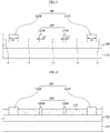
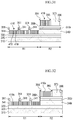
- FIGS. 1 to 10 are cross-sectional views explaining a method for fabricating a wire grid polarizer plate according to a first embodiment of the invention.
- a base substrate may include a light permeable substrate 110, a conductive layer 120, and a guide layer 130.
- the light permeable substrate 110 can transmit visible light and the material of the light permeable substrate 110 can be properly selected to match the purpose or processing thereof.
- the light permeable substrate 110 may include various polymer compounds, such as glass, quartz, acryl, triacetylcellulose ("TAC”), cyclic olefin copolymer (“COP”), cyclic olefin polymer (“COC”), polycarbonate (“PC”), polyethylene naphthalate (“PET”), polyimide (“PI”), polyethylene naphthalate (“PEN”), polyether sulfone (“PES”), and polyarylate (“PAR”), but is not limited thereto.
- the light permeable substrate 110 may include an optical film base material having a predetermined degree of flexibility.
- the conductive layer 120 may be disposed on the light permeable substrate 110.
- the conductive layer 120 may cover the whole surface of the light permeable substrate 110.
- the conductive layer 120 may include any conductive material without limitation.
- the conductive layer 120 may include a metal, and specifically, may include one of aluminum (Al), chrome (Cr), silver (Ag), copper (Cu), nickel (Ni), titanium (Ti), cobalt (Co), molybdenum (Mo), and an alloy thereof, but is not limited thereto.
- the conductive layer 120 may have a multilayer structure that includes two or more layers.
- a first conductive layer may include aluminum
- a second conductive layer may include titanium or molybdenum, but the first and second conductive layers are not limited thereto.
- the first conductive layer (not illustrated) includes aluminum
- hillocks may form or an upper surface thereof may become nonuniform depending on a processing temperature in the subsequent process, and this may cause the optical characteristic of a display device to deteriorate.
- the second conductive layer (not illustrated) that includes titanium or molybdenum may be disposed on the first conductive layer (not illustrated) so as to prevent the generation of hillocks in the process.
- the conductive layer 120 may be provided using sputtering, chemical vapor deposition, or evaporation, for example, but is not limited thereto.
- the guide layer 130 may be disposed on the conductive layer 120.
- the guide layer 130 may be a resin layer and the resin layer may be a photoresist layer, but it is not limited thereto.
- the guide layer 130 may cover the whole surface of the conductive layer 120.
- first guide pattern layers 1GP, 3GP, and T may include first and third guide patterns 1GP and 3GP and first trenches T.
- first guide partitions 131W and third guide partitions 131R may be formed by exposing and developing the guide layer 130 to match the pattern using a mask or the like.
- this is merely exemplary, and various patterning techniques may be used.
- the first guide pattern 1GP may include the first guide partitions 131W that are spaced apart from each other.
- the third guide pattern 3GP may include the third guide partitions 131R that are spaced apart from each other.
- the first trenches T may expose parts of the conductive layer 120 between the first guide partitions 131W, between the third guide partitions 131R, and between the first guide partitions 131W and the third guide partitions 131R.
- the first guide partitions 131W may be provided with a first width L1
- the third guide partitions 131R may be provided with a third width L3.
- the first width L1 may be narrower than the third width L3.
- the third width L3 of the third guide partitions 131R is wider than the first width L1 of the first guide partitions 131W.
- a trimming process may be performed to provide second and fourth guide patterns 2GP and 4GP through reduction of the widths of the first and third guide patterns 1GP and 3GP, for example.
- the first guide pattern layers 1GP, 3GP, and T may become the second guide pattern layers 2GP, 4GP, and T'.
- the first guide partitions 131W may become second guide partitions 131W'
- the third guide partitions 131R may become fourth guide partitions 131R'.
- the first trench T may become the second trench T'.
- a second width L2 of the second guide partitions 131W' becomes narrower than the first width L1 of the first guide partitions 131W
- a fourth width L4 of the fourth guide partitions 131R' becomes narrower than the third width L3 of the third guide partitions 131R.
- the width of the second trench T' becomes wider than the width of the first trench T. According to circumstances, through the trimming process, the width of the second guide partitions 131W' may be reduced even to a level which approaches or is substantially equal to the width of domains 141 and 142 (in FIG. 5 ) having self-aligned block copolymer nanostructures to be described later.
- the aperture ratio and the permeability of the wire grid polarizer plate may become heightened.
- the number of domains 141 and 142 (in FIG. 5 ) having self-assembled block copolymer nanostructures, which are to be provided in the second trench T' between the second and fourth guide partitions 131W' and 131R' may be increased, and thus the aperture ratio of the wire grid polarizer plate may be increased.
- the domains having the self-assembled block copolymer nanostructures will be described later with reference to FIG. 5 .
- the trimming process may be performed using a plasma etching process, for example.
- Plasma that is used in the trimming process is not specially limited so far as it can reduce the first and third widths L1 and L3 of the first and third guide partitions 131W and 131R.
- the trimming process may be performed using oxygen (O 2 ) plasma, for example.
- the second guide pattern 2GP may serve as a mask for forming third linear structures 3WS (in FIG. 13 ) of linear lattice patterns to be described later, and the fourth guide pattern 4GP may serve as a mask for forming reflective patterns RF (in FIG. 13 ) to be described later.
- the second guide pattern 2GP may include the second guide partitions 131W' that are spaced apart from each other, and the fourth guide pattern 4GP may include the fourth guide partitions 131R' that are spaced apart from each other.
- a block copolymer layer 140 may be provided in the second trench T' between the second and fourth guide partitions 131W' and 131R'.
- the block copolymer may include first repetition units and second repetition units.
- the block copolymer may include at least one of PS-b-PB(polystyrene-b-polybutadiene), PS-b-PI(polystyrene-b-polyisoprene), PS-b-PMMA(polystyrene-b-poly(methyl methacrylate)), PS-b-P2VP(polystyrene-b-poly(2-vinylpyridine)), PS-b-PFDMS(polystyrene-b-poly(ferrocenyl-dimethylsilane)), PS-b-PtBA(polystyrene-b-poly(tert-butylacrylate)), PS-b-PF
- the first repetition units and the second repetition units have different chemical properties.
- the first repetition units and the second repetition units may be microphase-separated through self-assembly.
- the first repetition units and the second repetition units have different etch rates.
- One of the first repetition units and the second repetition units may have a selective affinity with respect to the second and fourth guide partitions 131W' and 131R'. As described later, one of the first domains in which the first repetition units are self-aligned and the second domains in which the second repetition units are self-aligned may be selectively removed.
- a neutral layer may be disposed on a bottom portion of the second trench T', i.e., on the conductive layer 120 in the second trench T'.
- the neutral layer may be provided using a material that is almost similar to surface energy of the block copolymer. Since the neutral layer (not illustrated) does not have the selective affinity with respect to the first repetition units or the second repetition units of the block copolymer, it becomes possible to control vertical alignment of the first repetition units and the second repetition units of the block copolymer.
- the neutral layer may be random copolymers of monomers of the block copolymer, for example, but is not limited thereto.
- the random copolymer may include at least one of PS-r-PB(polystyrene-r-polybutadiene)), PS-r-PI(polystyrene-r-polyisoprene), PS-r-PMMA(polystyrene-r-poly(methyl methacrylate)), PS-r-P2VP(polystyrene-r-poly(2-vinylpyridine)), PS-r-PFDMS(polystyrene-r-poly(ferrocenyl-dimethylsilane)), PS-r-PtBA(polystyrene-r-poly(tert-butylacrylate)), PS-r-PFEMS(polystyrene-r-poly(ferrocenylethylmethylsilane)), PI-r-PEO(polyisoprene-r-poly(ethyleneoxide)), PB-r-PVP(polyr-
- surfaces of the second and fourth guide partitions 131W' and 131R' may be treated as hydrophobic surfaces.
- the hydrophobic surface treatment of the second and fourth guide partitions 131W' and 131R' may be performed through a fluoro polymer coating process or a fluoro gas plasma process, but is not limited thereto.
- the hydrophobic surface treatment of the second and fourth guide partitions 131W' and 131R' may be performed before the neutral layer (not illustrated) is provided.
- a self-assembled block copolymer nanostructure in which the first domains 141 and the second domains 142 are alternately arranged, may be provided.
- the self-assembled block copolymer nanostructure may include the first domains 141 and the second domains 142.
- the first domains 141 may include the first repetition units, and the second domains 142 may include the second repetition units.
- the first domains 141 may be provided through self-assembling of the first repetition units, and the second domains 142 may be provided through self-assembling of the second repetition units.
- the self-assembling process of the block copolymer 140 may be performed, for example, through annealing.
- the annealing includes thermal annealing and solvent annealing, for example.
- the thermal annealing is a method to guide microphase separation through heating over a glass transition temperature Tg of the block copolymer
- the solvent annealing is a method to guide microphase separation by exposing a polymer thin film including the block copolymer to solvent vapor.
- the first and third guide partitions 131W and 131R may be provided so that the height thereof after the trimming process thereof becomes equal to or higher than 2.5 times the height of the block copolymer layer 140, for example. Since swelling occurs as the solvent vaporized in the solvent annealing process infiltrates into the block copolymer, it is required to secure the above-described height so as to prevent the block copolymer from flowing out of the second trench T' (in FIG. 3 ) over the second and fourth guide partitions 131W' and 131R' (in FIG. 3 ).
- only the second domains 142 among the first domains 141 and the second domains 142 may be selectively removed.
- a process of selectively removing the second domains 142 among the first domains 141 and the second domains 142 may be performed using a solvent having high affinity to the second domains 142, but is not limited thereto.
- the second domains 142 may be selectively removed through a dry etching process.
- a gas that can be used in the dry etching may include at least one of oxygen (O 2 ), fluorocarbon gas, and hydrogen fluoride (HF), for example, but is not limited thereto.
- the fluorocarbon gas may include at least one of C 4 F 8 , CHF 3 , CH 2 F 2 , C 4 F 8 , CF 4 , and C 2 F 6 , for example, but is not limited thereto.
- a conductive pattern layer may be provided by patterning the conductive layer 120 using the second and fourth guide partitions 131W' and 131R' and the first domains 141 as a mask.
- the conductive pattern layer may include linear lattice patterns PT and reflective patterns RF.
- the linear lattice patterns PT may be provided so that conductive partitions 121D and 121W are spaced apart from each other at an interval of a period that is shorter than the wavelength of an incident light.
- the linear lattice patterns PT may transmit a first polarized light of the incident light and may reflect a second polarized light that is perpendicular to the first polarized light.
- the first polarized light may be a P-wave polarized light that is perpendicular to the conductive partitions 121D and 121W
- the second polarized light may be an S-wave polarized light that is in parallel to the conductive partitions 121W and 121D, for example.
- the conductive partitions 121W and 121D may have a line width of about 50 nanometers (nm) or less, a thickness of about 150 nm or more, and a pitch of about 100 nm, for example.
- the conductive partitions 121D may be provided through patterning of the conductive layer 120 of a region that is protected by the first domains 141, and the conductive partitions 121W may be provided through patterning of the conductive layer 120 of a region that is protected by the second guide partitions 131W'.
- the reflective patterns RF may be provided through patterning of the conductive layer 120 of a region that is protected by the fourth guide partitions 131R'.
- the reflective patterns RF may reflect both the first polarized light and the second polarized light of the incident light.
- the second polarized light that is reflected by the linear lattice patterns PT may be re-reflected by the reflective patterns RF to be incident to the linear lattice patterns PT.
- the reflective patterns RF may be arranged between the linear lattice patterns PT. This will be described in detail with reference to FIGS. 11 to 13 .
- the wire grid polarizer plate of FIG. 7 may include the light permeable substrate 110, the conductive partitions 121D, 121W, and 121R that are arranged in parallel to project from the light permeable substrate 110, the second and fourth guide partitions 131W' and 131R' positioned on the conductive partitions 121W and 121R, and the first domains 141 positioned on the conductive partitions 121D.
- the second and fourth guide partitions 131W' and 131R' and the first domains 141 may remain on the conductive partitions 121D, 121W, and 121R.
- the first domains 141 may be repeatedly arranged to be adjacent to each other between the second guide partitions 131W'.
- the first domains 141 may be repeatedly arranged to be adjacent to each other between the second guide partitions 131W' and the fourth guide partitions 131R'.
- the wire grid polarizer plate of FIG. 8 may include the light permeable substrate 110, the conductive partitions 121D, 121W, and 121R that are arranged in parallel to project from the light permeable substrate 110, the second and fourth guide partitions 131W' and 131R' positioned on the conductive partitions 121W and 121R.
- the wire grid polarizer plate of FIG. 8 is different from the wire grid polarizer plate of FIG. 7 on the point that the first domains 141 are not arranged on the conductive partitions 121D.
- the second and fourth guide partitions 131W' and 131R' may be arranged so that the conductive partitions 121D are interposed between them.
- the wire grid polarizer plate of FIG. 9 may include the light permeable substrate 110, the conductive partitions 121D, 121W, and 121R that are arranged in parallel to project from the light permeable substrate 110, and the first domains 141 positioned on the conductive partitions 121D.
- the wire grid polarizer plate of FIG. 9 is different from the wire grid polarizer plate of FIG. 7 on the point that the second and fourth guide partitions 131W' and 131R' are not arranged on the conductive partitions 121W and 121R.
- the first domains 141 may be arranged at a predetermined interval between the conductive partitions 121W and 121R.
- the wire grid polarizer plate of FIG. 10 may include the light permeable substrate 110, and the conductive partitions 121D, 121W, and 121R that are arranged in parallel to project from the light permeable substrate 110.
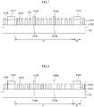
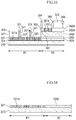
- FIG. 11 is a plan view of an intermediate product of FIG. 5
- FIG. 12 is an enlarged view of region A of FIG. 11 .
- second guide patterns 2GP including second guide partitions 131W' may be spaced apart from each other in a first direction D1
- fourth guide patterns 4GP including fourth guide partitions 131R' may be spaced apart from each other in the first direction D1 or second direction D2 so that second trenches T' are interposed between the fourth guide patterns 4GP.
- the second guide patterns 2GP may be connected to the fourth guide patterns 4GP.
- the second trench T' may be provided in a region that is surrounded by the second guide pattern 2GP and the fourth guide pattern 4GP, and may be provided, for example, in a straight hexagonal shape.
- the invention is not limited thereto, and the second trench T' may include various other shapes.
- self-aligned block copolymer nanostructures may be provided in the second trench T'.
- the self-aligned block copolymer nanostructure may include the first domains 141 and the second domains 142.
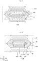
- the first domains 141 and the second domains 142 may provide first target patterns including polymer simple closed curves alternately arranged in the second trench T' from the center to the periphery.
- straight hexagonal polymer simple closed curves of the first domains 141 and straight hexagonal polymer simple closed curves of the second domains 142 may be alternately arranged in piles, in the second trench T' to provide the first target patterns, for example.
- the straight hexagonal polymer simple closed curves of the second domains 142 may surround outlines of the straight hexagonal polymer simple closed curves of the first domains 141 that are arranged on the inside, and the straight hexagonal polymer simple closed curves of the first domains 141 may surround outlines of the straight hexagonal polymer simple closed curves of the second domains 142 that are arranged on the inside so as to provide the first target patterns.
- the linear first domains 141, the linear second domains 142, or the linear first and second domains 141 and 142 may be arranged. That is, parts of the first domains 141 and the second domains 142 may not provide the straight hexagonal polymer simple closed curve.
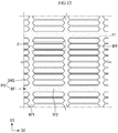
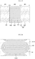
- FIG. 13 is a plan view of a wire grid polarizer plate of FIG. 10
- FIG. 14 is an enlarged view of region A of FIG. 13 .
- second target patterns may be provided in window regions WR using the first domains 141 as a mask
- third linear structures 3WS may be provided using the second guide partitions 131W' as a mask
- the reflective patterns RF may be provided using the fourth guide partitions 131R' as a mask.
- the wire grid polarizer plate may include the window regions WR and a frame region PR arranged on outlines of the window regions WR.
- the window regions WR are regions that correspond to the second trench T' (in FIG. 11 ), and in the window regions WR, the second target patterns including conductive simple closed curves surrounding in piles, spaced apart from each other at an interval of a period which is shorter than a wavelength of incident light may be provided..
- the second target patterns may include two or more polygonal conductive simple closed curves in which two first linear structures 1WS that extend in one direction and are spaced apart from each other and two or more second linear structures 2WS that do not extend in the one direction are connected to each other.
- the second target patterns may include the straight hexagonal conductive simple closed curves that are arranged in piles and spaced apart from each other.
- the straight hexagonal conductive simple closed curve may be a simple closed curve in which two first linear structures 1WS that extend in the second direction D2 and are spaced apart from each other in parallel, and four second linear structures 2WS that do not extend in the second direction D2 are connected to each other.
- the second linear structures 2WS may include two (2-1)-th linear structures 2-1WS that extend in a third direction D3 and two (2-2)-th linear structures 2-2WS that extend in a fourth direction D4.
- an angle ⁇ that is defined between the first linear structures 1WS and the second linear structures 2WS may be an obtuse angle, for example.
- an angle ⁇ that is defined between the (2-1)-th linear structures 2-1WS and the (2-2)-th linear structures 2-2WS may be an acute angle, for example.
- the conductive simple closed curves of the first and second linear structures 1WS and 2WS may be provided in the same shape as the polymer simple closed curve of the first domains 141. Accordingly, the conductive simple closed curves of the first and second linear structures 1WS and 2WS may be changed in accordance with the shape of the polymer simple closed curve of the first domains 141. In an exemplary embodiment, in the case where the shape of the polymer simple closed curve of the first domains 141 is a straight octagon, the conductive simple closed curve of the first and second linear structures 1WS and 2WS may be a straight octagon, for example.
- the frame region PR may include the third linear structures 3WS and the reflective patterns RF.
- the third linear structures 3WS may be arranged between the window regions WR. Since the second target patterns may be provided in the window regions WR, the third linear structures 3WS may be arranged between the second target patterns.
- the third linear structures 3WS may extend in the second direction D2 in which the first linear structures 1WS extend.
- the reflective patterns RF may include a first reflective region RF1 extending in the first direction D1, a second reflective region RF2 extending in the second direction D2, and a third reflective region Re disposed in a rectangular region (dotted line) that is circumscribed to the conductive simple closed curve on the outermost side of second target patterns.
- data wirings may extend in a direction that is in parallel to the first direction D1
- gate wirings may extend in a direction that is in parallel to the second direction D2.
- the first reflective region RF1 may overlap the data wirings (not illustrated)
- the second reflective region RF2 may overlap the gate wirings (not illustrated).
- the third reflective region Re may be connected to the first reflective region RF1 or the second reflective region RF2.
- the third reflective region Re may extend areas of the reflective patterns as large as areas that are obtained by subtracting areas of the conductive simple closed curves of the second target patterns from an area of the rectangular region (dotted line), and such extension of the areas of the reflective patterns RF may heighten the reflection efficiency of the second polarized light.
- the reflective patterns RF may be provided by patterning the conductive layer of the region that is protected by the fourth guide pattern 4GP, and may be connected to the third linear structures 3WS.
- the reflective patterns RF may be arranged between the linear lattice patterns PT.
- the wire grid polarizer plate may further include fourth linear structures (not illustrated) that correspond to the linear first domains 141, the linear second domains 142, or the linear first and second domains 141 and 142 which may be arranged on the inner side of the rectangular polymer simple closed curves on the innermost side of the first target patterns.
- the fourth linear structures (not illustrated) may be arranged in the arrangement direction of the first linear structures 1WS.
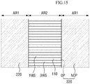
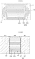
- FIG. 15 is a plan view illustrating an arrangement of a wire grid polarizer plate and an opaque layer of FIG. 11 .
- an opaque layer 220 may be arranged on an upper portion of a wire grid polarizer plate, and may include a non-opening portion NOP and openings OP.
- the opaque layer 220 may be a black matrix, for example.
- the non-opening portion NOP may cover the second linear structures 2WS of the second target patterns and the reflective patterns RF.
- First regions AR1 of the second target patterns may be covered by the non-opening portion NOP, and a second region AR2 may overlap the openings OP. Since the opaque layer 220 intercepts the incident light, the first polarized light that has penetrated the first regions AR1 of the second target patterns that are covered by the non-opening portion NOP is not emitted to an outside of the display device.
- the first regions AR1 and the second region AR2 may be divided on the basis of the second linear structures 2WS of the conductive simple closed curves on the innermost side of the second target patterns as boundaries, and the first regions AR1 may include regions in which the second linear structures 2WS of the conductive simple closed curves on the innermost side of the second target patterns are arranged.
- the second linear structures 2WS may be covered by the non-opening portion NOP. According to circumstances, parts of the first linear structures 1WS that are connected to the second linear structures 2WS may be covered by the non-opening portion NOP.
- the second region AR2 is a region in which the second linear structures 2WS of the conductive simple closed curves on the innermost side of the second target patterns are not arranged, and is arranged between the first regions AR1.
- the first linear structures 1WS are spaced apart from each other in a period that is shorter than the wavelength of the incident light in the second region AR2, and extend parallel to the second direction D2.
- the third linear structures 3WS may be spaced apart from the first linear structures 1WS in a period that is shorter than the wavelength of the incident light in a region that overlaps the opening OP, and may extend along the second direction D2.
- the light permeable substrate 110 may be arranged between the first linear structures 1WS and the third linear structures 3WS in the region that overlaps the opening OP.
- FIG. 16 is a partial cross-sectional view of a display device illustrating an arrangement of a wire grid polarizer plate and an opaque layer 220 of FIG. 10 .
- a wire grid polarizer plate may be arranged on a light permeable substrate 110, and a gate electrode G may be arranged on the wire grid polarizer plate.
- An insulating layer 150 may be arranged between the wire grid polarizer plate and the gate electrode G.
- the wire grid polarizer plate may be configured to include reflective patterns RF and linear lattice patterns PT, and the reflective patterns RF may be arranged in a region that overlaps an opaque layer 220.
- Linear lattice patterns PT that include conductive partitions 121W may be arranged in a region that overlaps a color filter 230.
- a thin film transistor may be configured as below.
- the gate electrode G is positioned on the transparent substrate 110, and a gate insulating layer GI is positioned on the gate electrode G.
- a semiconductor layer ACT is positioned in a region of which at least a part overlaps the gate electrode G on the gate insulating layer GI, and a source electrode S and a drain electrode D are positioned on the semiconductor layer ACT and spaced apart from each other.
- a passivation layer PL is positioned on the gate insulating layer GI, the source electrode S, the semiconductor layer ACT, and the drain electrode D, and a pixel electrode PE is positioned on the passivation layer PL and electrically connected to the drain electrode D via a contact hole that exposes at least a part of the drain electrode D.
- a liquid crystal layer 300 that includes liquid crystal molecules 301 may be arranged on an upper portion of the thin film transistor, and a color filter substrate may be arranged on an upper portion of the liquid crystal layer 300.
- the color filter substrate may have a structure in which the opaque layer 220 and red, green, and blue color filters 230 are disposed on the light permeable substrate 210.
- An overcoat layer 240 may be arranged on the opaque layer 220 and the color filters 230.
- the light permeable substrate 220 may include a transparent insulating material, such as glass or plastic, and the opaque layer 220 may be a black matrix for preventing light leakage.
- the color filters 230 may be arranged on both ends of the opaque layer 220.
- a common electrode which is an electric field generation electrode that includes a transparent conductive oxide, such as indium tin oxide ("ITO") or indium zinc oxide (“IZO”), may be further disposed on the overcoat layer 240.
- ITO indium tin oxide
- IZO indium
- the liquid crystal layer 300 serves to rotate the polarization axis of an incident light, and may be in a twisted nematic ("TN") mode having positive dielectric anisotropy, a vertical alignment (“VA”) mode, or a horizontal alignment (in-plane switching (“IPS”) or fringe field switching (“FFS”) mode, but is not limited thereto.
- TN twisted nematic
- VA vertical alignment
- IPS horizontal alignment
- FFS fringe field switching
- the display device may additionally include a backlight unit (not illustrated) that emits light, and an upper polarizer plate (not illustrated) that is arranged on an upper portion of the substrate 210.
- the backlight unit may further include, for example, a light guide plate, a light source portion, a reflective member, and optical sheets.
- the light guide plate is a portion that changes a path of light that is generated by the light source portion toward the liquid crystal layer, and may be provided with a light incident surface that is provided to make the light that is generated by the light source portion incident thereto and a light emission surface that is directed to the liquid crystal layer.
- the light guide plate may include a material having a predetermined refraction index, such as Poly Methyl Methacrylate (“PMMA”) that is one of light penetrating materials or Polycarbonate (“PC”), but is not limited thereto.
- the light which is incident to one side or both sides of the light guide plate that includes the above-described material has an angle that is within a critical angle of the light guide plate, it is incident to the inside of the light guide plate.
- the angle of the light deviates from the critical angle, and thus the light is not emitted to the outside of the light guide plate, but is uniformly transferred to the inside of the light guide plate.
- a scattering pattern may be disposed on any one of the upper and lower surfaces of the light guide plate, for example, on the lower surface that is opposite to the light emission surface, so that the guided light can be emitted to the upper portion thereof. That is, the scattering pattern may be printed, for example, with ink, on one surface of the light guide plate so that the light that is transferred from the inside of the light guide plate can be emitted to the upper portion thereof.
- the scattering pattern may be provided by printing ink, but is not limited thereto. Micro grooves or projections may be defined in the light guide plate, or various modifications thereof can be made.
- a reflective member may be further provided between the light guide plate and a bottom portion of a lower accommodation member.
- the reflective member serves to re-reflect the light that is emitted to the lower surface of the light guide plate, i.e., to an opposite surface that faces the light emission surface, and to supply the reflected light to the light guide plate.
- the reflective member may be in a film shape, but is not limited thereto.
- the light source portion may face the light incident surface of the light guide plate.
- the number of light source portions may be appropriately changed.
- one light source portion may be provided only on one side surface of the light guide plate, or three or more light source portions may be provided to correspond to three or more of four side surfaces of the light guide plate.
- a side light type that is a type in which light sources are positioned on the side surfaces of the light guide plate has been exemplified.
- a direct type or a surface-shaped light source type may be provided depending on the backlight configuration.
- the light source may include a white LED that emits white light, or a plurality of LEDs that emits red (R) light, green (G) light, and blue (B) light, respectively, for example.
- a plurality of light sources is implemented by LEDs that emit the red (R) light, green (G) light, and blue (B) light, respectively, the LEDs may be simultaneously turned on to implement white light through color mixing.
- the second target patterns may be non-polygonal simple closed curves of two first linear structures that extend in one direction and two or more second structures that do not extend in the one direction.
- the non-polygonal simple closed curve may include a modified straight hexagonal simple closed curve of which at least one short side is a curve.
- FIG. 17 is a view illustrating a first modified example of FIG. 12
- FIG. 18 is a view illustrating a first modified example of a wire grid polarizer plate of FIG. 14 .
- the first target patterns may have a structure in which the first domains 141 that include modified straight hexagonal polymer simple closed curves and the second domains 142 that include modified straight hexagonal polymer simple closed curves are alternately arranged in piles.
- the modified straight hexagonal polymer simple closed curve may be a modified straight hexagonal simple closed curve of which short sides are modified into curves.
- the second target patterns of FIG. 18 may include modified straight hexagonal simple closed curves having the same shape as the polymer simple closed curves of the first domains 141.
- the second target patterns may include at least two conductive simple closed curves including two first linear structures 1WS that are in parallel to each other, two (2-1)-th structures 2-1WS that are in a curved shape, and two (2-2)-th structures 2-2WS that are in a curved shape.
- the second target patterns of FIG. 18 are different from the second target patterns of FIG. 14 on the point that the (2-1)-th structures 2-1WS and the (2-2)-th structures 2-2WS are in a curved shape whereas the second linear structures 2WS are in a linear shape.
- FIG. 19 is a plan view illustrating an arrangement of a wire grid polarizer plate and an opaque layer of FIG. 18 .
- the arrangement of the wire grid polarizer plate and the opaque layer of FIG. 18 is the same as the arrangement of the wire grid polarizer plate and the opaque layer of FIG. 14 as described above with reference to FIG. 15 except that the (2-1)-th structures 2-1WS and the (2-2)-th structures 2-2WS, which are in a curved shape, are arranged in the first regions AR1, and the non-opening portion NOP covers the (2-1)-th structures 2-1WS and the (2-2)-th structures 2-2WS, which are in a curved shape.
- FIG. 20 is a view illustrating a second modified example of FIG. 12
- FIG. 21 is a view illustrating a second modified example of a wire grid polarizer plate of FIG. 14 .
- the first and second target patterns may have a structure in which at least two simple closed curves including two circular arch type structures are arranged in piles and spaced apart from each other.
- the first and second target patterns of FIGS. 20 and 21 are different from the first and second target patterns of FIGS. 12 and 14 on the point that the target patterns of FIGS. 20 and 21 include the simple closed curves of the two circular arch type structures whereas the target patterns of FIGS. 12 and 14 include the straight hexagonal simple closed curves.
- the arch type structure may have a structure that includes a curved portion and a support portion that supports the curved portion, and for example, the support portion may be in a linear shape.
- non-polygonal simple closed curves of the arch type structures are not limited to the simple closed curves of the two circular arch type structures, but may be two or more simple closed curves among a circular arch structure, a segment arch structure, a horseshoe arch structure, a pointed arch structure, and an ogee arch structure, circular simple closed curves, or elliptical simple closed curves.
- the first target patterns may have a structure in which the first domains 141 that include modified rectangular polymer simple closed curves and the second domains 142 that include modified rectangular polymer simple closed curves are alternately arranged in piles.
- the modified rectangular polymer simple closed curve may be a modified rectangular simple closed curve of which short sides are modified into curves.
- the second target patterns of FIG. 21 may include modified rectangular simple closed curves having the same shape as the polymer simple closed curves of the first domains 141.
- the second target patterns may include at least two conductive simple closed curves including two first linear structures 1WS that are in parallel to each other and two second linear structures 2WS that are in a circular arc shape.
- the second target patterns of FIG. 21 are different from the second target patterns of FIG. 14 on the point that the second linear structures 2WS are in a circular arc shape whereas the second linear structures 2WS of the second target patterns of FIG. 14 are in a linear shape.
- FIG. 22 is a plan view illustrating an arrangement of a wire grid polarizer plate and an opaque layer 220 of FIG. 21 .
- the arrangement of the wire grid polarizer plate and the opaque layer of FIG. 21 is the same as the arrangement of the wire grid polarizer plate and the opaque layer of FIG. 14 as described above with reference to FIG. 15 except that the second linear structures 2WS in a circular arc shape are arranged in the first regions AR1, and the non-opening portion NOP covers the second linear structures 2WS in a circular arc shape.
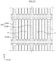
- FIG. 23 is a plan view of a first modified example of an intermediate product of FIG. 11 .
- An intermediate product of FIG. 23 is different from the intermediate product of FIG. 11 on the point that the second guide partitions 131W' and the second trenches T' are arranged in parallel to the first direction D1 in the intermediate product of FIG. 23 whereas the second guide partitions 131W' and the second trenches T' are arranged in parallel to the second direction D2 in the intermediate product of FIG. 11 .
- FIG. 24 is a plan view of a second modified example of an intermediate product of FIG. 11 .
- An intermediate product of FIG. 24 is different from the intermediate product of FIG. 11 on the point that the second guide partitions 131W' and the second trenches T' are arranged in parallel to the third direction D3 in the intermediate product of FIG. 24 whereas the second guide partitions 131W' and the second trenches T' are arranged in parallel to the second direction D2 in the intermediate product of FIG. 11 .
- FIGS. 25 to 34 are cross-sectional views explaining a method for fabricating a wire grid polarizer plate according to a second embodiment of the invention.
- a base substrate may include a light permeable substrate 310, conductive layers 320 and 330, a guide layer 340, a hard mask layer 350, a capping layer 360, and a sacrificial layer 370.
- the light permeable substrate 310 can transmit visible light and the material of the light permeable substrate 310 can be properly selected to match the purpose or processing thereof. Since the light permeable substrate 310 has been described, the detailed explanation thereof will be omitted.
- the conductive layers 320 and 330 may include any conductive material without limit.
- the conductive layers 320 and 330 may entirely cover the light permeable substrate 310.
- the conductive layers 320 and 330 may include the first conductive layer 320 and the second conductive layer 330.
- the first conductive layer 320 may include one of aluminum (Al), chrome (Cr), silver (Ag), copper (Cu), nickel (Ni), titanium (Ti), cobalt (Co), molybdenum (Mo), and an alloy thereof, but is not limited thereto.
- the second conductive layer 330 may include a material having an etch rate that is lower than the etch rate of the first conductive layer 320.
- the first conductive layer 320 may include aluminum, and the second conductive layer 330 may include titanium or molybdenum, but are not limited thereto.
- the guide layer 340 may be disposed on the second conductive layer 330.
- the guide layer 340 may entirely cover the second conductive layer 330.
- the guide layer 340 may include a material having an etch rate that is higher than the etch rate of the second conductive layer 330.
- the guide layer 340 may include silicon nitride (SiNx), for example, but is not limited thereto.
- the hard mask layer 350 may be disposed on the guide layer 340.
- the hard mask layer 350 may entirely cover the guide layer 340.
- the hard mask layer 350 may include a material having an etch rate that is lower than the etch rate of the guide layer 340.
- the hard mask layer 50 may include aluminum (Al), but is not limited thereto.
- the capping layer 360 may be disposed on the hard mask layer 350.
- the capping layer 360 may entirely cover the hard mask layer 350.
- the capping layer 360 can prevent hillock phenomenon of the hard mask layer 350 from occurring.
- the capping layer 360 may include a material having an etch rate that is lower than the etch rate of the hard mask layer 350.
- the capping layer 360 may include titanium (Ti), but is not limited thereto.
- the capping layer 360 may be omitted.
- the sacrificial layer 370 may be disposed on the hard mask layer 350.
- the sacrificial layer 370 may entirely cover the hard mask layer 350.
- the sacrificial layer 370 may include a material having an etch rate that is higher than the etch rate of the capping layer 360.
- the sacrificial layer 370 may include silicon nitride (SiNx), for example, but is not limited thereto.
- a first photosensitive film pattern layer 380 may be disposed on the sacrificial layer 370.
- the first photosensitive film pattern layer 380 may be provided using a photolithography method, for example.
- First photosensitive film patterns 381, 382, and 383 may be arranged on the sacrificial layer 370 and spaced apart from one another, and parts of the sacrificial layer 370 may be exposed between the first photosensitive film patterns 381, 382, and 383.
- sacrificial layer patterns 371, 372, and 373 may be disposed on the capping layer 360.
- the sacrificial layer patterns 371, 372, and 373 may be provided by patterning the sacrificial layer 370 using the first photosensitive film patterns 381, 382, and 383 as a mask.
- a spacer layer 390 may be disposed on the sacrificial layer patterns 371, 372, and 373 and the capping layer 360.
- the spacer layer 390 may entirely cover the sacrificial layer patterns 371, 372, and 373 and the capping layer 360 that is exposed between the sacrificial layer patterns 371, 372, and 373.
- the spacer layer 390 may include silicon oxide (SiOx), for example.
- spacer patterns 391, 392, 393, 394, 395, and 396 may be provided by patterning the spacer layer 390. Specifically, the spacer patterns 391, 392, 393, 394, 395, and 396 may cover side surfaces of the sacrificial layer patterns 371, 372, and 373. Parts of the capping layer 360 may be exposed between the spacer patterns 391, 392, 393, 394, 395, and 396. Upper surfaces of the sacrificial layer patterns 371, 372, and 373 may be exposed between the spacer patterns 391, 392, 393, 394, 395, and 396.
- a second photosensitive film pattern 400 may be disposed only on the second region R2 of the first and second regions R1 and R2.
- the first region R1 is a region in which a linear lattice pattern PT (in FIG. 34 ) is to be provided later
- the second region R2 is a region in which a reflective pattern RF (in FIG. 34 ) is to be provided later.
- the second photosensitive film pattern 400 can protect the region in which the reflective pattern RF (in FIG. 34 ) is to be provided.
- the sacrificial layers 371 and 372 may be selectively removed from the first region R1 only. Since the sacrificial layer 373 is protected by the second photosensitive film pattern 400, the sacrificial layer 373 is not removed unlike the sacrificial layers 371 and 372. After the sacrificial layers 371 and 372 are removed, parts of the capping layer 360 may be exposed between the spacer patterns 394, 395, and 396 in the first region R1.
- the hard mask layer 350 and the guide layer 340 in the first region R1 may be patterned using the spacer patterns 391, 392, and 393 as a mask in a state where the second region R2 is protected by the second photosensitive film pattern 400.
- the first hard mask pattern 351 and a guide pattern 341 may be disposed on the second conductive layer 330.
- parts of the capping layer 360 may remain on the hard mask pattern 351.
- the guide pattern 341 in the first region or the guide pattern 341 and the first hard mask pattern 351 may correspond to the first guide pattern 1GP (refer to FIG. 2 ) as described above.
- the second photosensitive film pattern 400 may be removed after the first hard mask pattern 351 and the guide pattern 341 are provided.
- a first residual capping layer pattern 360r, a first residual hard mask pattern 350r, and a residual guide pattern 340r may be disposed in the second region R2.
- the residual guide pattern 340r or the first residual capping layer pattern 360r, the first residual hard mask pattern 350r, and the residual guide pattern 340r may correspond to the third guide pattern 3GP (refer to FIG. 2 ) as described above.
- a self-assembled block copolymer layer 410 may be disposed between the guide patterns 341 and between the spacer patterns 394 and 395.
- the self-assembled block copolymer layer 410 may include first domains 410a and second domains 410b. Since the self-assembled block copolymer layer 410 has been described, the detailed explanation thereof will be omitted.
- a neutral layer (not illustrated) may be disposed on a bottom portion of the trench, i.e., on the second conductive layer 330 in the trench, to control vertical alignment of first repetition units and second repetition units of the block copolymer. Since the neutral layer has been described, the detailed explanation thereof will be omitted.
- the surface of the guide pattern 341 may be treated as a hydrophobic surface.
- the hydrophobic surface treatment of the guide pattern 341 may be performed through a fluoro polymer coating process or a fluoro gas plasma process, for example, but is not limited thereto.
- only the second domains 410b of the first and second domains 410a and 410b may be selectively removed.
- a process of selectively removing the second domains 410b of the first and second domains 410a and 410b may be performed using a solvent having high affinity as described above.
- the conductive layers 320 and 330 may be patterned using the first domains 410a and the guide pattern 341 as a mask in the first region R1.
- First conductive pattern layers 321 and 321a and second conductive pattern layers 331 and 331a may be disposed in the first region R1.
- the first conductive pattern layers 321 and 321a may be arranged on lower portions of the second conductive pattern layers 331 and 331a.
- a first residual capping layer pattern 360r and a first residual hard mask pattern 350r may be patterned using the spacer patterns 394, 395, and 396 and the sacrificial layer pattern 373 as a mask.
- capping layer patterns 361 and 361a, second hard mask patterns 351 and 351a, second residual capping layer pattern 360rr, and a second residual hard mask pattern 350rr may be provided. Further, as a result of patterning the conductive layers 320 and 330 in the first region R1, residual conductive patterns 320r and 330r may be disposed in the second region R2.
- only the first conductive patterns 321 and 321a and the residual conductive pattern 320r may be disposed on the light permeable substrate 310.
- the first conductive patterns 321 and 321a may provide the linear lattice pattern PT, and the residual conductive pattern 320r may provide the reflective pattern RF.
- the first conductive pattern 321a may correspond to the linear structures 121W (refer to FIG. 10 ) as described above, and the first conductive pattern layer 321 may correspond to the fourth linear structure 121R (refer to FIG. 10 ) as described above.
Landscapes
- Physics & Mathematics (AREA)
- Nonlinear Science (AREA)
- General Physics & Mathematics (AREA)
- Optics & Photonics (AREA)
- Mathematical Physics (AREA)
- Chemical & Material Sciences (AREA)
- Crystallography & Structural Chemistry (AREA)
- Polarising Elements (AREA)
Applications Claiming Priority (1)
| Application Number | Priority Date | Filing Date | Title |
|---|---|---|---|
| KR1020150057980A KR102413901B1 (ko) | 2015-04-24 | 2015-04-24 | 와이어 그리드 편광판 및 이를 포함하는 표시장치 |
Publications (2)
| Publication Number | Publication Date |
|---|---|
| EP3086146A1 EP3086146A1 (en) | 2016-10-26 |
| EP3086146B1 true EP3086146B1 (en) | 2018-09-26 |
Family
ID=55808355
Family Applications (1)
| Application Number | Title | Priority Date | Filing Date |
|---|---|---|---|
| EP16163992.7A Active EP3086146B1 (en) | 2015-04-24 | 2016-04-06 | Display device including a wire grid polarizer plate and method of manufacturing |
Country Status (4)
| Country | Link |
|---|---|
| US (1) | US9915768B2 (ko) |
| EP (1) | EP3086146B1 (ko) |
| KR (1) | KR102413901B1 (ko) |
| CN (1) | CN106066504B (ko) |
Families Citing this family (2)
| Publication number | Priority date | Publication date | Assignee | Title |
|---|---|---|---|---|
| CN108803124B (zh) * | 2018-06-27 | 2021-05-28 | 武汉华星光电技术有限公司 | 曲面液晶显示屏及其制造方法 |
| JP7317939B2 (ja) * | 2019-03-07 | 2023-07-31 | 富士フイルム株式会社 | 偏光素子および画像表示装置 |
Family Cites Families (19)
| Publication number | Priority date | Publication date | Assignee | Title |
|---|---|---|---|---|
| US7304719B2 (en) * | 2004-03-31 | 2007-12-04 | Asml Holding N.V. | Patterned grid element polarizer |
| KR20080024316A (ko) | 2006-09-13 | 2008-03-18 | 엘지전자 주식회사 | 선 격자 편광자의 제조 방법 |
| KR20100110358A (ko) | 2008-02-08 | 2010-10-12 | 램 리써치 코포레이션 | 이중 마스크 자기정렬 이중 패터닝 기술 (sadpt) 프로세스 |
| US20110141422A1 (en) * | 2008-08-19 | 2011-06-16 | Risuke Yanagawa | Liquid crystal display device |
| JP2010224232A (ja) * | 2009-03-24 | 2010-10-07 | Stanley Electric Co Ltd | 液晶表示素子及びその製造方法 |
| US8248696B2 (en) * | 2009-06-25 | 2012-08-21 | Moxtek, Inc. | Nano fractal diffuser |
| KR20110101893A (ko) | 2010-03-10 | 2011-09-16 | 삼성전자주식회사 | 액정 표시 장치 |
| KR20120105694A (ko) | 2011-03-16 | 2012-09-26 | 동우 화인켐 주식회사 | 광시야각 액정표시장치 |
| US8913320B2 (en) * | 2011-05-17 | 2014-12-16 | Moxtek, Inc. | Wire grid polarizer with bordered sections |
| KR101942363B1 (ko) * | 2012-07-26 | 2019-04-12 | 삼성디스플레이 주식회사 | 편광 소자, 이의 제조 방법, 이를 포함하는 표시 패널 및 이를 포함하는 표시 장치 |
| US8771929B2 (en) * | 2012-08-16 | 2014-07-08 | International Business Machines Corporation | Tone inversion of self-assembled self-aligned structures |
| KR20140030382A (ko) | 2012-08-27 | 2014-03-12 | 삼성디스플레이 주식회사 | 액정 표시 장치 및 이의 제조 방법 |
| KR102003334B1 (ko) | 2012-09-04 | 2019-07-24 | 삼성전자주식회사 | 패턴 형성 방법 |
| KR20140087904A (ko) | 2012-12-31 | 2014-07-09 | 삼성전자주식회사 | 블록 코폴리머 층의 패턴 형성 방법 |
| KR20140137734A (ko) | 2013-05-23 | 2014-12-03 | 삼성디스플레이 주식회사 | 반사형 편광판 제조방법 및 인셀 반사형 편광판 제조방법 |
| KR20150029817A (ko) | 2013-09-10 | 2015-03-19 | 삼성디스플레이 주식회사 | 편광판, 이를 갖는 표시장치 및 이의 제조방법 |
| CN104330915B (zh) * | 2014-11-07 | 2017-06-06 | 京东方科技集团股份有限公司 | 一种阵列基板、液晶显示面板及显示装置 |
| EP3023820B1 (en) | 2014-11-18 | 2023-12-27 | Samsung Display Co., Ltd. | Wire grid polarizing plate, display device including the same, and method of fabricating said display device |
| CN104459863A (zh) * | 2014-12-04 | 2015-03-25 | 京东方科技集团股份有限公司 | 线栅偏光片及其制备方法、显示面板和显示装置 |
-
2015
- 2015-04-24 KR KR1020150057980A patent/KR102413901B1/ko active IP Right Grant
-
2016
- 2016-01-07 US US14/990,334 patent/US9915768B2/en active Active
- 2016-04-06 EP EP16163992.7A patent/EP3086146B1/en active Active
- 2016-04-18 CN CN201610238149.2A patent/CN106066504B/zh active Active
Non-Patent Citations (1)
| Title |
|---|
| None * |
Also Published As
| Publication number | Publication date |
|---|---|
| CN106066504A (zh) | 2016-11-02 |
| KR102413901B1 (ko) | 2022-06-28 |
| US20160313481A1 (en) | 2016-10-27 |
| EP3086146A1 (en) | 2016-10-26 |
| US9915768B2 (en) | 2018-03-13 |
| KR20160127255A (ko) | 2016-11-03 |
| CN106066504B (zh) | 2020-08-28 |
Similar Documents
| Publication | Publication Date | Title |
|---|---|---|
| US10295717B2 (en) | Wire grid polarizing plate, display device including the same, and method of fabricating said display device | |
| KR102305200B1 (ko) | 와이어 그리드 편광자, 이를 포함하는 표시 장치 및 이의 제조방법 | |
| KR102226116B1 (ko) | 와이어 그리드 편광자 및 이의 제조방법 | |
| US20160124265A1 (en) | Polarizer, method for manufacturing polarizer and display panel | |
| CN105700056B (zh) | 偏振板、包括该偏振板的tft基板及制造该偏振板的方法 | |
| EP3023821A1 (en) | Wire grid polarizer, display device including the same and method for fabricating the same | |
| US9612379B2 (en) | Wire grid polarizer and method of fabricating the same | |
| EP3086146B1 (en) | Display device including a wire grid polarizer plate and method of manufacturing | |
| US20160170115A1 (en) | Wire grid polarizer and method of manufacturing the same | |
| US9488765B2 (en) | Wire grid polarizer and method of fabricating the same | |
| US20160077377A1 (en) | Wire grid polarizer, display device including the same and method for fabricating the same | |
| KR102241418B1 (ko) | 와이어 그리드 편광자 및 이의 제조방법 | |
| KR102255379B1 (ko) | 표시 장치 및 이를 제조하는 방법 | |
| KR102133211B1 (ko) | 와이어 그리드 편광자의 제조방법 | |
| KR102410299B1 (ko) | 와이어 그리드 편광판, 이를 포함하는 표시장치 및 표시장치의 제조방법 | |
| US20160266294A1 (en) | Wire grid polarizer and method of fabricating the same | |
| KR20210085716A (ko) | 액정표시장치 | |
| KR20150133921A (ko) | 액정 표시패널 제조방법 |
Legal Events
| Date | Code | Title | Description |
|---|---|---|---|
| PUAI | Public reference made under article 153(3) epc to a published international application that has entered the european phase |
Free format text: ORIGINAL CODE: 0009012 |
|
| AK | Designated contracting states |
Kind code of ref document: A1 Designated state(s): AL AT BE BG CH CY CZ DE DK EE ES FI FR GB GR HR HU IE IS IT LI LT LU LV MC MK MT NL NO PL PT RO RS SE SI SK SM TR |
|
| AX | Request for extension of the european patent |
Extension state: BA ME |
|
| STAA | Information on the status of an ep patent application or granted ep patent |
Free format text: STATUS: REQUEST FOR EXAMINATION WAS MADE |
|
| 17P | Request for examination filed |
Effective date: 20170223 |
|
| RBV | Designated contracting states (corrected) |
Designated state(s): AL AT BE BG CH CY CZ DE DK EE ES FI FR GB GR HR HU IE IS IT LI LT LU LV MC MK MT NL NO PL PT RO RS SE SI SK SM TR |
|
| GRAP | Despatch of communication of intention to grant a patent |
Free format text: ORIGINAL CODE: EPIDOSNIGR1 |
|
| STAA | Information on the status of an ep patent application or granted ep patent |
Free format text: STATUS: GRANT OF PATENT IS INTENDED |
|
| INTG | Intention to grant announced |
Effective date: 20180409 |
|
| GRAS | Grant fee paid |
Free format text: ORIGINAL CODE: EPIDOSNIGR3 |
|
| GRAA | (expected) grant |
Free format text: ORIGINAL CODE: 0009210 |
|
| STAA | Information on the status of an ep patent application or granted ep patent |
Free format text: STATUS: THE PATENT HAS BEEN GRANTED |
|
| AK | Designated contracting states |
Kind code of ref document: B1 Designated state(s): AL AT BE BG CH CY CZ DE DK EE ES FI FR GB GR HR HU IE IS IT LI LT LU LV MC MK MT NL NO PL PT RO RS SE SI SK SM TR |
|
| REG | Reference to a national code |
Ref country code: GB Ref legal event code: FG4D |
|
| REG | Reference to a national code |
Ref country code: CH Ref legal event code: EP |
|
| REG | Reference to a national code |
Ref country code: AT Ref legal event code: REF Ref document number: 1046695 Country of ref document: AT Kind code of ref document: T Effective date: 20181015 |
|
| REG | Reference to a national code |
Ref country code: IE Ref legal event code: FG4D |
|
| REG | Reference to a national code |
Ref country code: DE Ref legal event code: R096 Ref document number: 602016005862 Country of ref document: DE |
|
| REG | Reference to a national code |
Ref country code: NL Ref legal event code: MP Effective date: 20180926 |
|
| PG25 | Lapsed in a contracting state [announced via postgrant information from national office to epo] |
Ref country code: GR Free format text: LAPSE BECAUSE OF FAILURE TO SUBMIT A TRANSLATION OF THE DESCRIPTION OR TO PAY THE FEE WITHIN THE PRESCRIBED TIME-LIMIT Effective date: 20181227 Ref country code: SE Free format text: LAPSE BECAUSE OF FAILURE TO SUBMIT A TRANSLATION OF THE DESCRIPTION OR TO PAY THE FEE WITHIN THE PRESCRIBED TIME-LIMIT Effective date: 20180926 Ref country code: RS Free format text: LAPSE BECAUSE OF FAILURE TO SUBMIT A TRANSLATION OF THE DESCRIPTION OR TO PAY THE FEE WITHIN THE PRESCRIBED TIME-LIMIT Effective date: 20180926 Ref country code: FI Free format text: LAPSE BECAUSE OF FAILURE TO SUBMIT A TRANSLATION OF THE DESCRIPTION OR TO PAY THE FEE WITHIN THE PRESCRIBED TIME-LIMIT Effective date: 20180926 Ref country code: LT Free format text: LAPSE BECAUSE OF FAILURE TO SUBMIT A TRANSLATION OF THE DESCRIPTION OR TO PAY THE FEE WITHIN THE PRESCRIBED TIME-LIMIT Effective date: 20180926 Ref country code: BG Free format text: LAPSE BECAUSE OF FAILURE TO SUBMIT A TRANSLATION OF THE DESCRIPTION OR TO PAY THE FEE WITHIN THE PRESCRIBED TIME-LIMIT Effective date: 20181226 Ref country code: NO Free format text: LAPSE BECAUSE OF FAILURE TO SUBMIT A TRANSLATION OF THE DESCRIPTION OR TO PAY THE FEE WITHIN THE PRESCRIBED TIME-LIMIT Effective date: 20181226 |
|
| REG | Reference to a national code |
Ref country code: LT Ref legal event code: MG4D |
|
| PG25 | Lapsed in a contracting state [announced via postgrant information from national office to epo] |
Ref country code: AL Free format text: LAPSE BECAUSE OF FAILURE TO SUBMIT A TRANSLATION OF THE DESCRIPTION OR TO PAY THE FEE WITHIN THE PRESCRIBED TIME-LIMIT Effective date: 20180926 Ref country code: LV Free format text: LAPSE BECAUSE OF FAILURE TO SUBMIT A TRANSLATION OF THE DESCRIPTION OR TO PAY THE FEE WITHIN THE PRESCRIBED TIME-LIMIT Effective date: 20180926 Ref country code: HR Free format text: LAPSE BECAUSE OF FAILURE TO SUBMIT A TRANSLATION OF THE DESCRIPTION OR TO PAY THE FEE WITHIN THE PRESCRIBED TIME-LIMIT Effective date: 20180926 |
|
| REG | Reference to a national code |
Ref country code: AT Ref legal event code: MK05 Ref document number: 1046695 Country of ref document: AT Kind code of ref document: T Effective date: 20180926 |
|
| PG25 | Lapsed in a contracting state [announced via postgrant information from national office to epo] |
Ref country code: AT Free format text: LAPSE BECAUSE OF FAILURE TO SUBMIT A TRANSLATION OF THE DESCRIPTION OR TO PAY THE FEE WITHIN THE PRESCRIBED TIME-LIMIT Effective date: 20180926 Ref country code: EE Free format text: LAPSE BECAUSE OF FAILURE TO SUBMIT A TRANSLATION OF THE DESCRIPTION OR TO PAY THE FEE WITHIN THE PRESCRIBED TIME-LIMIT Effective date: 20180926 Ref country code: IS Free format text: LAPSE BECAUSE OF FAILURE TO SUBMIT A TRANSLATION OF THE DESCRIPTION OR TO PAY THE FEE WITHIN THE PRESCRIBED TIME-LIMIT Effective date: 20190126 Ref country code: PL Free format text: LAPSE BECAUSE OF FAILURE TO SUBMIT A TRANSLATION OF THE DESCRIPTION OR TO PAY THE FEE WITHIN THE PRESCRIBED TIME-LIMIT Effective date: 20180926 Ref country code: ES Free format text: LAPSE BECAUSE OF FAILURE TO SUBMIT A TRANSLATION OF THE DESCRIPTION OR TO PAY THE FEE WITHIN THE PRESCRIBED TIME-LIMIT Effective date: 20180926 Ref country code: RO Free format text: LAPSE BECAUSE OF FAILURE TO SUBMIT A TRANSLATION OF THE DESCRIPTION OR TO PAY THE FEE WITHIN THE PRESCRIBED TIME-LIMIT Effective date: 20180926 Ref country code: NL Free format text: LAPSE BECAUSE OF FAILURE TO SUBMIT A TRANSLATION OF THE DESCRIPTION OR TO PAY THE FEE WITHIN THE PRESCRIBED TIME-LIMIT Effective date: 20180926 Ref country code: CZ Free format text: LAPSE BECAUSE OF FAILURE TO SUBMIT A TRANSLATION OF THE DESCRIPTION OR TO PAY THE FEE WITHIN THE PRESCRIBED TIME-LIMIT Effective date: 20180926 Ref country code: IT Free format text: LAPSE BECAUSE OF FAILURE TO SUBMIT A TRANSLATION OF THE DESCRIPTION OR TO PAY THE FEE WITHIN THE PRESCRIBED TIME-LIMIT Effective date: 20180926 |
|
| PG25 | Lapsed in a contracting state [announced via postgrant information from national office to epo] |
Ref country code: PT Free format text: LAPSE BECAUSE OF FAILURE TO SUBMIT A TRANSLATION OF THE DESCRIPTION OR TO PAY THE FEE WITHIN THE PRESCRIBED TIME-LIMIT Effective date: 20190126 Ref country code: SM Free format text: LAPSE BECAUSE OF FAILURE TO SUBMIT A TRANSLATION OF THE DESCRIPTION OR TO PAY THE FEE WITHIN THE PRESCRIBED TIME-LIMIT Effective date: 20180926 Ref country code: SK Free format text: LAPSE BECAUSE OF FAILURE TO SUBMIT A TRANSLATION OF THE DESCRIPTION OR TO PAY THE FEE WITHIN THE PRESCRIBED TIME-LIMIT Effective date: 20180926 |
|
| REG | Reference to a national code |
Ref country code: DE Ref legal event code: R097 Ref document number: 602016005862 Country of ref document: DE |
|
| PG25 | Lapsed in a contracting state [announced via postgrant information from national office to epo] |
Ref country code: DK Free format text: LAPSE BECAUSE OF FAILURE TO SUBMIT A TRANSLATION OF THE DESCRIPTION OR TO PAY THE FEE WITHIN THE PRESCRIBED TIME-LIMIT Effective date: 20180926 |
|
| PLBE | No opposition filed within time limit |
Free format text: ORIGINAL CODE: 0009261 |
|
| STAA | Information on the status of an ep patent application or granted ep patent |
Free format text: STATUS: NO OPPOSITION FILED WITHIN TIME LIMIT |
|
| 26N | No opposition filed |
Effective date: 20190627 |
|
| PG25 | Lapsed in a contracting state [announced via postgrant information from national office to epo] |
Ref country code: SI Free format text: LAPSE BECAUSE OF FAILURE TO SUBMIT A TRANSLATION OF THE DESCRIPTION OR TO PAY THE FEE WITHIN THE PRESCRIBED TIME-LIMIT Effective date: 20180926 |
|
| REG | Reference to a national code |
Ref country code: CH Ref legal event code: PL |
|
| REG | Reference to a national code |
Ref country code: BE Ref legal event code: MM Effective date: 20190430 |
|
| PG25 | Lapsed in a contracting state [announced via postgrant information from national office to epo] |
Ref country code: LU Free format text: LAPSE BECAUSE OF NON-PAYMENT OF DUE FEES Effective date: 20190406 Ref country code: MC Free format text: LAPSE BECAUSE OF FAILURE TO SUBMIT A TRANSLATION OF THE DESCRIPTION OR TO PAY THE FEE WITHIN THE PRESCRIBED TIME-LIMIT Effective date: 20180926 |
|
| PG25 | Lapsed in a contracting state [announced via postgrant information from national office to epo] |
Ref country code: CH Free format text: LAPSE BECAUSE OF NON-PAYMENT OF DUE FEES Effective date: 20190430 Ref country code: LI Free format text: LAPSE BECAUSE OF NON-PAYMENT OF DUE FEES Effective date: 20190430 |
|
| PG25 | Lapsed in a contracting state [announced via postgrant information from national office to epo] |
Ref country code: BE Free format text: LAPSE BECAUSE OF NON-PAYMENT OF DUE FEES Effective date: 20190430 |
|
| PG25 | Lapsed in a contracting state [announced via postgrant information from national office to epo] |
Ref country code: TR Free format text: LAPSE BECAUSE OF FAILURE TO SUBMIT A TRANSLATION OF THE DESCRIPTION OR TO PAY THE FEE WITHIN THE PRESCRIBED TIME-LIMIT Effective date: 20180926 |
|
| PG25 | Lapsed in a contracting state [announced via postgrant information from national office to epo] |
Ref country code: IE Free format text: LAPSE BECAUSE OF NON-PAYMENT OF DUE FEES Effective date: 20190406 |
|
| PG25 | Lapsed in a contracting state [announced via postgrant information from national office to epo] |
Ref country code: CY Free format text: LAPSE BECAUSE OF FAILURE TO SUBMIT A TRANSLATION OF THE DESCRIPTION OR TO PAY THE FEE WITHIN THE PRESCRIBED TIME-LIMIT Effective date: 20180926 |
|
| PG25 | Lapsed in a contracting state [announced via postgrant information from national office to epo] |
Ref country code: HU Free format text: LAPSE BECAUSE OF FAILURE TO SUBMIT A TRANSLATION OF THE DESCRIPTION OR TO PAY THE FEE WITHIN THE PRESCRIBED TIME-LIMIT; INVALID AB INITIO Effective date: 20160406 Ref country code: MT Free format text: LAPSE BECAUSE OF FAILURE TO SUBMIT A TRANSLATION OF THE DESCRIPTION OR TO PAY THE FEE WITHIN THE PRESCRIBED TIME-LIMIT Effective date: 20180926 |
|
| PG25 | Lapsed in a contracting state [announced via postgrant information from national office to epo] |
Ref country code: MK Free format text: LAPSE BECAUSE OF FAILURE TO SUBMIT A TRANSLATION OF THE DESCRIPTION OR TO PAY THE FEE WITHIN THE PRESCRIBED TIME-LIMIT Effective date: 20180926 |
|
| PGFP | Annual fee paid to national office [announced via postgrant information from national office to epo] |
Ref country code: FR Payment date: 20230321 Year of fee payment: 8 |
|
| P01 | Opt-out of the competence of the unified patent court (upc) registered |
Effective date: 20230516 |
|
| PGFP | Annual fee paid to national office [announced via postgrant information from national office to epo] |
Ref country code: DE Payment date: 20230320 Year of fee payment: 8 |
|
| PGFP | Annual fee paid to national office [announced via postgrant information from national office to epo] |
Ref country code: GB Payment date: 20240320 Year of fee payment: 9 |