EP3085215B1 - Abschirmungsprodukte für elektromagnetische interferenz (emi) unter verwendung von material auf der basis von titanmonoxid (tio) - Google Patents
Abschirmungsprodukte für elektromagnetische interferenz (emi) unter verwendung von material auf der basis von titanmonoxid (tio) Download PDFInfo
- Publication number
- EP3085215B1 EP3085215B1 EP14827314.7A EP14827314A EP3085215B1 EP 3085215 B1 EP3085215 B1 EP 3085215B1 EP 14827314 A EP14827314 A EP 14827314A EP 3085215 B1 EP3085215 B1 EP 3085215B1
- Authority
- EP
- European Patent Office
- Prior art keywords
- composition
- loss tangent
- ghz
- composite material
- item
- Prior art date
- Legal status (The legal status is an assumption and is not a legal conclusion. Google has not performed a legal analysis and makes no representation as to the accuracy of the status listed.)
- Active
Links
- KELHQGOVULCJSG-UHFFFAOYSA-N n,n-dimethyl-1-(5-methylfuran-2-yl)ethane-1,2-diamine Chemical compound CN(C)C(CN)C1=CC=C(C)O1 KELHQGOVULCJSG-UHFFFAOYSA-N 0.000 title claims description 82
- 239000000463 material Substances 0.000 title description 36
- 239000002131 composite material Substances 0.000 claims description 117
- 239000000203 mixture Substances 0.000 claims description 104
- 239000002245 particle Substances 0.000 claims description 86
- 239000011159 matrix material Substances 0.000 claims description 71
- 239000000919 ceramic Substances 0.000 claims description 52
- 230000005291 magnetic effect Effects 0.000 claims description 34
- XEEYBQQBJWHFJM-UHFFFAOYSA-N Iron Chemical compound [Fe] XEEYBQQBJWHFJM-UHFFFAOYSA-N 0.000 claims description 22
- 230000000116 mitigating effect Effects 0.000 claims description 11
- 229910009493 Y3Fe5O12 Inorganic materials 0.000 claims description 7
- 230000001629 suppression Effects 0.000 claims description 2
- 229920000642 polymer Polymers 0.000 description 60
- 239000000976 ink Substances 0.000 description 49
- 239000004593 Epoxy Substances 0.000 description 32
- 239000010410 layer Substances 0.000 description 30
- 239000010408 film Substances 0.000 description 26
- 229920001577 copolymer Polymers 0.000 description 24
- 238000000034 method Methods 0.000 description 21
- OKTJSMMVPCPJKN-UHFFFAOYSA-N Carbon Chemical compound [C] OKTJSMMVPCPJKN-UHFFFAOYSA-N 0.000 description 20
- 239000000843 powder Substances 0.000 description 20
- NBVXSUQYWXRMNV-UHFFFAOYSA-N fluoromethane Chemical compound FC NBVXSUQYWXRMNV-UHFFFAOYSA-N 0.000 description 19
- 239000002033 PVDF binder Substances 0.000 description 18
- 239000004020 conductor Substances 0.000 description 18
- 229920002981 polyvinylidene fluoride Polymers 0.000 description 17
- 239000002904 solvent Substances 0.000 description 17
- 239000000945 filler Substances 0.000 description 15
- 239000007787 solid Substances 0.000 description 12
- 238000000576 coating method Methods 0.000 description 11
- GWEVSGVZZGPLCZ-UHFFFAOYSA-N Titan oxide Chemical compound O=[Ti]=O GWEVSGVZZGPLCZ-UHFFFAOYSA-N 0.000 description 10
- 229910021389 graphene Inorganic materials 0.000 description 10
- 239000000523 sample Substances 0.000 description 10
- 230000035699 permeability Effects 0.000 description 9
- 239000000047 product Substances 0.000 description 9
- 229910000859 α-Fe Inorganic materials 0.000 description 9
- 239000011248 coating agent Substances 0.000 description 8
- 235000012489 doughnuts Nutrition 0.000 description 8
- 229910052751 metal Inorganic materials 0.000 description 7
- 239000002184 metal Substances 0.000 description 7
- 238000012360 testing method Methods 0.000 description 7
- LFQSCWFLJHTTHZ-UHFFFAOYSA-N Ethanol Chemical compound CCO LFQSCWFLJHTTHZ-UHFFFAOYSA-N 0.000 description 6
- OKKJLVBELUTLKV-UHFFFAOYSA-N Methanol Chemical compound OC OKKJLVBELUTLKV-UHFFFAOYSA-N 0.000 description 6
- ZMXDDKWLCZADIW-UHFFFAOYSA-N N,N-Dimethylformamide Chemical compound CN(C)C=O ZMXDDKWLCZADIW-UHFFFAOYSA-N 0.000 description 6
- 239000007788 liquid Substances 0.000 description 6
- 239000004033 plastic Substances 0.000 description 6
- 239000002861 polymer material Substances 0.000 description 6
- 229910052799 carbon Inorganic materials 0.000 description 5
- 229910010293 ceramic material Inorganic materials 0.000 description 5
- 230000002209 hydrophobic effect Effects 0.000 description 5
- BQCIDUSAKPWEOX-UHFFFAOYSA-N 1,1-Difluoroethene Chemical compound FC(F)=C BQCIDUSAKPWEOX-UHFFFAOYSA-N 0.000 description 4
- ZAMOUSCENKQFHK-UHFFFAOYSA-N Chlorine atom Chemical compound [Cl] ZAMOUSCENKQFHK-UHFFFAOYSA-N 0.000 description 4
- KFZMGEQAYNKOFK-UHFFFAOYSA-N Isopropanol Chemical compound CC(C)O KFZMGEQAYNKOFK-UHFFFAOYSA-N 0.000 description 4
- SECXISVLQFMRJM-UHFFFAOYSA-N N-Methylpyrrolidone Chemical compound CN1CCCC1=O SECXISVLQFMRJM-UHFFFAOYSA-N 0.000 description 4
- VYPSYNLAJGMNEJ-UHFFFAOYSA-N Silicium dioxide Chemical compound O=[Si]=O VYPSYNLAJGMNEJ-UHFFFAOYSA-N 0.000 description 4
- WYURNTSHIVDZCO-UHFFFAOYSA-N Tetrahydrofuran Chemical compound C1CCOC1 WYURNTSHIVDZCO-UHFFFAOYSA-N 0.000 description 4
- 229910052801 chlorine Inorganic materials 0.000 description 4
- 239000000460 chlorine Substances 0.000 description 4
- 239000008119 colloidal silica Substances 0.000 description 4
- 239000000470 constituent Substances 0.000 description 4
- 239000011521 glass Substances 0.000 description 4
- 229910002804 graphite Inorganic materials 0.000 description 4
- 239000010439 graphite Substances 0.000 description 4
- HCDGVLDPFQMKDK-UHFFFAOYSA-N hexafluoropropylene Chemical group FC(F)=C(F)C(F)(F)F HCDGVLDPFQMKDK-UHFFFAOYSA-N 0.000 description 4
- 239000000696 magnetic material Substances 0.000 description 4
- 238000005259 measurement Methods 0.000 description 4
- 239000002064 nanoplatelet Substances 0.000 description 4
- 239000012188 paraffin wax Substances 0.000 description 4
- 229920000058 polyacrylate Polymers 0.000 description 4
- 229920000570 polyether Polymers 0.000 description 4
- 229920001296 polysiloxane Polymers 0.000 description 4
- 238000007639 printing Methods 0.000 description 4
- 230000004044 response Effects 0.000 description 4
- 239000000758 substrate Substances 0.000 description 4
- 229920001897 terpolymer Polymers 0.000 description 4
- BFKJFAAPBSQJPD-UHFFFAOYSA-N tetrafluoroethene Chemical group FC(F)=C(F)F BFKJFAAPBSQJPD-UHFFFAOYSA-N 0.000 description 4
- 238000012546 transfer Methods 0.000 description 4
- 239000001993 wax Substances 0.000 description 4
- UHOVQNZJYSORNB-UHFFFAOYSA-N Benzene Chemical compound C1=CC=CC=C1 UHOVQNZJYSORNB-UHFFFAOYSA-N 0.000 description 3
- 229910052782 aluminium Inorganic materials 0.000 description 3
- XAGFODPZIPBFFR-UHFFFAOYSA-N aluminium Chemical compound [Al] XAGFODPZIPBFFR-UHFFFAOYSA-N 0.000 description 3
- 230000000052 comparative effect Effects 0.000 description 3
- 239000000975 dye Substances 0.000 description 3
- 230000005670 electromagnetic radiation Effects 0.000 description 3
- 238000002156 mixing Methods 0.000 description 3
- PXHVJJICTQNCMI-UHFFFAOYSA-N nickel Substances [Ni] PXHVJJICTQNCMI-UHFFFAOYSA-N 0.000 description 3
- 239000000049 pigment Substances 0.000 description 3
- 239000004408 titanium dioxide Substances 0.000 description 3
- CSCPPACGZOOCGX-UHFFFAOYSA-N Acetone Chemical compound CC(C)=O CSCPPACGZOOCGX-UHFFFAOYSA-N 0.000 description 2
- 229920000049 Carbon (fiber) Polymers 0.000 description 2
- 238000010521 absorption reaction Methods 0.000 description 2
- 229910045601 alloy Inorganic materials 0.000 description 2
- 239000000956 alloy Substances 0.000 description 2
- 238000013459 approach Methods 0.000 description 2
- -1 articles Substances 0.000 description 2
- 230000008901 benefit Effects 0.000 description 2
- 230000005540 biological transmission Effects 0.000 description 2
- 230000000903 blocking effect Effects 0.000 description 2
- 239000003990 capacitor Substances 0.000 description 2
- 239000004917 carbon fiber Substances 0.000 description 2
- 229910021393 carbon nanotube Inorganic materials 0.000 description 2
- 239000002041 carbon nanotube Substances 0.000 description 2
- 239000002270 dispersing agent Substances 0.000 description 2
- 239000006185 dispersion Substances 0.000 description 2
- 239000002019 doping agent Substances 0.000 description 2
- 238000001035 drying Methods 0.000 description 2
- 238000005516 engineering process Methods 0.000 description 2
- 230000005293 ferrimagnetic effect Effects 0.000 description 2
- 230000005294 ferromagnetic effect Effects 0.000 description 2
- 239000006260 foam Substances 0.000 description 2
- 239000002223 garnet Substances 0.000 description 2
- 238000011065 in-situ storage Methods 0.000 description 2
- 229910052742 iron Inorganic materials 0.000 description 2
- 238000011068 loading method Methods 0.000 description 2
- 229910001092 metal group alloy Inorganic materials 0.000 description 2
- 239000002082 metal nanoparticle Substances 0.000 description 2
- 239000002923 metal particle Substances 0.000 description 2
- BFXIKLCIZHOAAZ-UHFFFAOYSA-N methyltrimethoxysilane Chemical compound CO[Si](C)(OC)OC BFXIKLCIZHOAAZ-UHFFFAOYSA-N 0.000 description 2
- 238000004377 microelectronic Methods 0.000 description 2
- 239000002070 nanowire Substances 0.000 description 2
- 229910052759 nickel Inorganic materials 0.000 description 2
- 239000008188 pellet Substances 0.000 description 2
- 239000002243 precursor Substances 0.000 description 2
- 239000000126 substance Substances 0.000 description 2
- 239000004094 surface-active agent Substances 0.000 description 2
- YLQBMQCUIZJEEH-UHFFFAOYSA-N tetrahydrofuran Natural products C=1C=COC=1 YLQBMQCUIZJEEH-UHFFFAOYSA-N 0.000 description 2
- 239000010936 titanium Substances 0.000 description 2
- UWSYCPWEBZRZNJ-UHFFFAOYSA-N trimethoxy(2,4,4-trimethylpentyl)silane Chemical compound CO[Si](OC)(OC)CC(C)CC(C)(C)C UWSYCPWEBZRZNJ-UHFFFAOYSA-N 0.000 description 2
- 229910017518 Cu Zn Inorganic materials 0.000 description 1
- 229910017752 Cu-Zn Inorganic materials 0.000 description 1
- 229910017943 Cu—Zn Inorganic materials 0.000 description 1
- 229920006368 Hylar Polymers 0.000 description 1
- 229910018605 Ni—Zn Inorganic materials 0.000 description 1
- ATJFFYVFTNAWJD-UHFFFAOYSA-N Tin Chemical compound [Sn] ATJFFYVFTNAWJD-UHFFFAOYSA-N 0.000 description 1
- RTAQQCXQSZGOHL-UHFFFAOYSA-N Titanium Chemical compound [Ti] RTAQQCXQSZGOHL-UHFFFAOYSA-N 0.000 description 1
- 239000011358 absorbing material Substances 0.000 description 1
- 239000000853 adhesive Substances 0.000 description 1
- 230000001070 adhesive effect Effects 0.000 description 1
- 239000012790 adhesive layer Substances 0.000 description 1
- QVGXLLKOCUKJST-UHFFFAOYSA-N atomic oxygen Chemical compound [O] QVGXLLKOCUKJST-UHFFFAOYSA-N 0.000 description 1
- 229920005601 base polymer Polymers 0.000 description 1
- 229910052796 boron Inorganic materials 0.000 description 1
- 229910052804 chromium Inorganic materials 0.000 description 1
- 238000004891 communication Methods 0.000 description 1
- 150000001875 compounds Chemical class 0.000 description 1
- 239000013068 control sample Substances 0.000 description 1
- 229910052802 copper Inorganic materials 0.000 description 1
- 230000007547 defect Effects 0.000 description 1
- 230000003292 diminished effect Effects 0.000 description 1
- 238000009826 distribution Methods 0.000 description 1
- 230000000694 effects Effects 0.000 description 1
- 230000005684 electric field Effects 0.000 description 1
- 239000012777 electrically insulating material Substances 0.000 description 1
- 239000008393 encapsulating agent Substances 0.000 description 1
- 230000001747 exhibiting effect Effects 0.000 description 1
- 229910052731 fluorine Inorganic materials 0.000 description 1
- 239000011888 foil Substances 0.000 description 1
- ZSOJHTHUCUGDHS-UHFFFAOYSA-N gadolinium iron Chemical compound [Fe].[Gd] ZSOJHTHUCUGDHS-UHFFFAOYSA-N 0.000 description 1
- 229910052737 gold Inorganic materials 0.000 description 1
- 230000005661 hydrophobic surface Effects 0.000 description 1
- 239000012535 impurity Substances 0.000 description 1
- 239000011810 insulating material Substances 0.000 description 1
- 239000012212 insulator Substances 0.000 description 1
- 239000013067 intermediate product Substances 0.000 description 1
- 229910052740 iodine Inorganic materials 0.000 description 1
- MTRJKZUDDJZTLA-UHFFFAOYSA-N iron yttrium Chemical compound [Fe].[Y] MTRJKZUDDJZTLA-UHFFFAOYSA-N 0.000 description 1
- 229910052748 manganese Inorganic materials 0.000 description 1
- 238000004519 manufacturing process Methods 0.000 description 1
- 238000000691 measurement method Methods 0.000 description 1
- 230000007246 mechanism Effects 0.000 description 1
- 239000004200 microcrystalline wax Substances 0.000 description 1
- 235000019808 microcrystalline wax Nutrition 0.000 description 1
- 239000003607 modifier Substances 0.000 description 1
- 229910052750 molybdenum Inorganic materials 0.000 description 1
- 239000004570 mortar (masonry) Substances 0.000 description 1
- 238000000465 moulding Methods 0.000 description 1
- 229910052758 niobium Inorganic materials 0.000 description 1
- 229910052757 nitrogen Inorganic materials 0.000 description 1
- 239000003921 oil Substances 0.000 description 1
- 239000001301 oxygen Substances 0.000 description 1
- 229910052760 oxygen Inorganic materials 0.000 description 1
- 239000013500 performance material Substances 0.000 description 1
- 229910000889 permalloy Inorganic materials 0.000 description 1
- 229910052698 phosphorus Inorganic materials 0.000 description 1
- 229910052697 platinum Inorganic materials 0.000 description 1
- 230000000063 preceeding effect Effects 0.000 description 1
- 230000008569 process Effects 0.000 description 1
- 229910052707 ruthenium Inorganic materials 0.000 description 1
- 229910000702 sendust Inorganic materials 0.000 description 1
- 229910052710 silicon Inorganic materials 0.000 description 1
- 239000010703 silicon Substances 0.000 description 1
- 229910052709 silver Inorganic materials 0.000 description 1
- 125000006850 spacer group Chemical group 0.000 description 1
- 238000003756 stirring Methods 0.000 description 1
- 229910052717 sulfur Inorganic materials 0.000 description 1
- 239000006188 syrup Substances 0.000 description 1
- 235000020357 syrup Nutrition 0.000 description 1
- 229910052719 titanium Inorganic materials 0.000 description 1
- XLYOFNOQVPJJNP-UHFFFAOYSA-N water Substances O XLYOFNOQVPJJNP-UHFFFAOYSA-N 0.000 description 1
- 238000005303 weighing Methods 0.000 description 1
Images

Classifications
-
- H—ELECTRICITY
- H05—ELECTRIC TECHNIQUES NOT OTHERWISE PROVIDED FOR
- H05K—PRINTED CIRCUITS; CASINGS OR CONSTRUCTIONAL DETAILS OF ELECTRIC APPARATUS; MANUFACTURE OF ASSEMBLAGES OF ELECTRICAL COMPONENTS
- H05K9/00—Screening of apparatus or components against electric or magnetic fields
- H05K9/0073—Shielding materials
- H05K9/0081—Electromagnetic shielding materials, e.g. EMI, RFI shielding
- H05K9/0083—Electromagnetic shielding materials, e.g. EMI, RFI shielding comprising electro-conductive non-fibrous particles embedded in an electrically insulating supporting structure, e.g. powder, flakes, whiskers
-
- C—CHEMISTRY; METALLURGY
- C08—ORGANIC MACROMOLECULAR COMPOUNDS; THEIR PREPARATION OR CHEMICAL WORKING-UP; COMPOSITIONS BASED THEREON
- C08K—Use of inorganic or non-macromolecular organic substances as compounding ingredients
- C08K3/00—Use of inorganic substances as compounding ingredients
- C08K3/18—Oxygen-containing compounds, e.g. metal carbonyls
- C08K3/20—Oxides; Hydroxides
- C08K3/22—Oxides; Hydroxides of metals
-
- H—ELECTRICITY
- H05—ELECTRIC TECHNIQUES NOT OTHERWISE PROVIDED FOR
- H05K—PRINTED CIRCUITS; CASINGS OR CONSTRUCTIONAL DETAILS OF ELECTRIC APPARATUS; MANUFACTURE OF ASSEMBLAGES OF ELECTRICAL COMPONENTS
- H05K9/00—Screening of apparatus or components against electric or magnetic fields
- H05K9/0073—Shielding materials
- H05K9/0081—Electromagnetic shielding materials, e.g. EMI, RFI shielding
-
- C—CHEMISTRY; METALLURGY
- C08—ORGANIC MACROMOLECULAR COMPOUNDS; THEIR PREPARATION OR CHEMICAL WORKING-UP; COMPOSITIONS BASED THEREON
- C08K—Use of inorganic or non-macromolecular organic substances as compounding ingredients
- C08K3/00—Use of inorganic substances as compounding ingredients
- C08K3/18—Oxygen-containing compounds, e.g. metal carbonyls
- C08K3/20—Oxides; Hydroxides
- C08K3/22—Oxides; Hydroxides of metals
- C08K2003/2206—Oxides; Hydroxides of metals of calcium, strontium or barium
-
- C—CHEMISTRY; METALLURGY
- C08—ORGANIC MACROMOLECULAR COMPOUNDS; THEIR PREPARATION OR CHEMICAL WORKING-UP; COMPOSITIONS BASED THEREON
- C08K—Use of inorganic or non-macromolecular organic substances as compounding ingredients
- C08K3/00—Use of inorganic substances as compounding ingredients
- C08K3/18—Oxygen-containing compounds, e.g. metal carbonyls
- C08K3/20—Oxides; Hydroxides
- C08K3/22—Oxides; Hydroxides of metals
- C08K2003/221—Oxides; Hydroxides of metals of rare earth metal
-
- C—CHEMISTRY; METALLURGY
- C08—ORGANIC MACROMOLECULAR COMPOUNDS; THEIR PREPARATION OR CHEMICAL WORKING-UP; COMPOSITIONS BASED THEREON
- C08K—Use of inorganic or non-macromolecular organic substances as compounding ingredients
- C08K3/00—Use of inorganic substances as compounding ingredients
- C08K3/18—Oxygen-containing compounds, e.g. metal carbonyls
- C08K3/20—Oxides; Hydroxides
- C08K3/22—Oxides; Hydroxides of metals
- C08K2003/2237—Oxides; Hydroxides of metals of titanium
-
- C—CHEMISTRY; METALLURGY
- C08—ORGANIC MACROMOLECULAR COMPOUNDS; THEIR PREPARATION OR CHEMICAL WORKING-UP; COMPOSITIONS BASED THEREON
- C08K—Use of inorganic or non-macromolecular organic substances as compounding ingredients
- C08K3/00—Use of inorganic substances as compounding ingredients
- C08K3/18—Oxygen-containing compounds, e.g. metal carbonyls
- C08K3/20—Oxides; Hydroxides
- C08K3/22—Oxides; Hydroxides of metals
- C08K2003/2265—Oxides; Hydroxides of metals of iron
-
- C—CHEMISTRY; METALLURGY
- C08—ORGANIC MACROMOLECULAR COMPOUNDS; THEIR PREPARATION OR CHEMICAL WORKING-UP; COMPOSITIONS BASED THEREON
- C08K—Use of inorganic or non-macromolecular organic substances as compounding ingredients
- C08K3/00—Use of inorganic substances as compounding ingredients
- C08K3/18—Oxygen-containing compounds, e.g. metal carbonyls
- C08K3/20—Oxides; Hydroxides
- C08K3/22—Oxides; Hydroxides of metals
- C08K2003/2289—Oxides; Hydroxides of metals of cobalt
Definitions
- compositions including articles, molded bodies, and printable inks, that can be used to reduce electromagnetic interference (EMI) when applied to a workpiece such as an electrical or electronic circuit, circuit component, or enclosure containing such a circuit or circuit component.
- EMI electromagnetic interference
- the disclosure also relates to associated articles, systems, and methods.
- EMI electromagnetic interference
- the EMI may originate from a variety of sources, including in many cases the electrical sources and electronic devices themselves.
- Radio, television, and other communication systems are also sources of EMI which can disrupt the functioning of the electronic devices, causing diminished performance or even device failure.
- the blocking may be for the purpose of reducing the amount of EMI radiating outwardly from a given circuit or circuit component, reducing the amount of EMI radiating inwardly towards the circuit or circuit component from other sources, or both.
- the blocking also known as shielding, can be achieved by reflection of the EMI, absorption of the EMI, or a combination of both.
- a metal sheet or foil known as an EM shield, which has high electrical conductivity, is used to reflect the undesired EMI. Reflecting the EMI may, however, in some cases be insufficient and may cause further problems.
- Ceramics are not usually associated with high dielectric loss in the radio frequency or microwave ranges. They are instead generally considered to be good electrically insulating materials. However, we have found that certain ceramic materials, in particular titanium monoxide (TiO), either alone or in combination with one or more additional components, can provide a surprisingly high dielectric loss, magnetic loss, or both, even at gigahertz (GHz) frequencies.
- TiO titanium monoxide
- the TiO can be dispersed as particulates in a matrix material to produce composite materials that can be shaped, coated, printed, molded, or otherwise used in various product configurations for the purpose of mitigating EMI.
- Compositions as well as products such as flexible films, molded bodies, and printable inks can incorporate ceramic particles comprising titanium monoxide (TiO) and, when used, the one or more additional components, to provide substantial electromagnetic interference (EMI) mitigation at megahertz through gigahertz frequencies.
- the films and bodies, as well as the printed inks after the removal of solvent comprise a composite material which includes the ceramic TiO particles and, when used, the one or more additional components, dispersed within a matrix material, such as a polymer.
- the composite material may have a loss tangent, such as a dielectric loss tangent, a magnetic loss tangent, or both, of at least 0.03, or at least 0.1, or at least 0.3, or at least 0.4 over a frequency range from 1 GHz to 5 GHz.
- a component of the loss tangent due to the ceramic particles may be at least 0.01, or at least 0.05, or at least 0.1 over such frequency range.
- the dielectric loss tangent is a measure of how much a material absorbs or dissipates electromagnetic radiation, and is discussed further below.
- compositions, articles, and inks that include a composite material for mitigating EMI.
- the composite material includes a matrix material and ceramic particles dispersed within the matrix material, and the ceramic particles are or include titanium monoxide (TiO).
- the ceramic particles may constitute a portion of the composite material, the portion being at least 10 vol. %, or at least 15 vol. % but no more than 60 vol. %, or at least 25 vol. % but no more than 50 vol. %.
- the composite material may have a dielectric loss tangent of at least 0.03, or at least 0.1, or at least 0.3, or at least 0.4, over a range from 1 GHz to 5 GHz.
- the dielectric loss tangent of the composite material may have a first loss tangent component due to the ceramic particles and a second loss tangent component due to the matrix material, and the first loss tangent component may be at least 0.1, or at least 0.2, or at least 0.3, over the range from 1 GHz to 5 GHz.
- the second loss tangent component may be at least 0.01, or at least 0.05, over the range from 1 GHz to 5 GHz.
- the matrix material may be or include a polymeric matrix material, and the polymeric matrix material may be or include a fluorocarbon-based polymer, a chlorine-containing polymer, a (meth) acrylate polymer, a silicone, an epoxy-based polymer, a polyether polymer, a copolymer thereof, or a combination thereof.
- the polymeric matrix material may be or include a fluorocarbon-based polymer or copolymer, and the fluorocarbon-based polymer or copolymer may be or include a polyvinylidene fluoride (PVDF) polymer or copolymer.
- PVDF polyvinylidene fluoride
- the fluorocarbon-based polymer or copolymer may be or include a terpolymer of tetrafluoroethylene, hexafluoropropylene, and vinylidene fluoride.
- the article may be or include a cable having one or more conductive lines, one or more of which may be at least partially surrounded by an EMI shielding layer, the EMI shielding layer comprising the composite material.
- the article may be or include a flexible EMI shielding layer that comprises the composite material, and such article may further include a film that carries the EMI shielding layer.
- the article may also be or include a rigid/molded body having a contoured shape.
- the ink including a matrix solution and ceramic particles dispersed within the matrix solution, where the ceramic particles are or include titanium monoxide (TiO).
- the matrix solution may be or include a polymer dissolved in a solvent, and the polymer may be or include a fluorocarbon-based polymer or copolymer.
- the fluorocarbon-based polymer or copolymer may, in turn, be or include a polyvinylidene fluoride (PVDF) polymer or copolymer.
- PVDF polyvinylidene fluoride
- the ink may be configured to produce, after the solvent is removed, a solid and/or cured composite material having the polymer as a matrix material and the ceramic particles dispersed in the matrix material, the solid/cured composite material having a dielectric loss tangent of at least 0.03, or at least 0.1, or at least 0.3, or at least 0.4, over a range from 1 GHz to 5 GHz.
- the ceramic particles may make up a portion of the solid/cured composite material, the portion being at least 10 vol. %, or at least 15 vol. % but no more than 60 vol. %, or at least 25 vol. % but no more than 50 vol. %.
- TiO refers to the chemical titanium monoxide, and not to a subunit of titania, TiO 2 , or titanium dioxide. Thus, a composition containing titanium dioxide does not necessarily contain TiO, and would not typically contain TiO unless TiO is also added to the composition as a separate material from the titanium dioxide.
- Composite materials can be used to make EMI shielding films, tapes, molded bodies, inks, and other products that are useful at least at frequencies of one to several gigahertz, as well as at lower frequencies (e.g. 10 MHz to 950 MHz or to 1 GHz) and higher frequencies (e.g. up to 60 GHz, for example, in a range from 1 to 60 GHz).
- the composite materials can provide significant attenuation of unwanted electromagnetic radiation or EMI at such frequencies due to the substantial dielectric loss tangent of the material, which we have measured.
- the composite materials comprise particles dispersed in a matrix material, and the particles, which are typically responsible for the great majority of the overall dielectric loss of the composite material, can be made of an inorganic, ceramic material, most commonly titanium monoxide (TiO).
- the TiO can be used either alone or in conjunction with one or more additional components.
- the additional components can be substances that attenuate EMI, enhance the EMI attenuating effects of TiO, or both.
- Exemplary additional components include nanosilica, such as hydrophobic nanosilica (i.e. nanosilica with a hydrophobic surface modifier), carbonyl iron, Ba 3 Co 3 Fe 24 O 41 , and Y 3 Fe 5 O 12 .
- a representative EMI attenuating material is shown schematically as composite material 120 in FIG. 1 .
- the composite material 120 may consist of, or may consist essentially of, or may simply comprise, along with one or more other constituent elements, ceramic particles 122 dispersed in a matrix material 121.
- One or more additional components may also be included, typically in particulate of powder form.
- the particles 122 may be composed entirely of pure TiO, keeping in mind that other elements or compounds may also be present as impurities in such particles. In other cases, the particles 122 may not be pure TiO (as in the case of doped TiO or reduced TiO).
- the dopant can be any suitable dopant, such as one or more of Cu, Co, Ni, Cr, Mn, Mo, Nb, V Fe, Ru, Au Ag, Pt, N, S, C, B, P, I, and F.
- the doping levels can vary widely, such as from 20 ppm or 50 ppm to 5 wt. % of the TiO or 5 wt% of the TiO.
- the TiO is reduced, the resulting material will be non-stoichiomentric, having a ratio of Ti:O of less than 1.
- the particles 122 need not have any particular shape, size, or size distribution, but may have a variety of shapes and sizes. In some cases, the particles 122 may be at least approximately spherical.
- the particles 122 may have particle sizes, or an average particle size, no less than 20 mn, no less than 30 nm, no less than 40 nm, no less than 50 nm, no less than 75 nm, no less than 100 nm, no less than 250 nm, no less than 375 nm, or no less than 0.5 microns, and no more than 100 microns, no more than 75 microns, no more than 60 microns, no more than 50 microns, or no more than 40 microns.
- the particle sizes, or an average particle size is in a range from 50 nm to 50 microns, more typically from 0.5 microns to 10 microns.
- shapes other than spheres and sizes other than those mentioned can also be used.
- the particles 122 are present in the composite material 120 in an amount that is more than merely a trace amount.
- the particles 122 may comprise or make up a portion of the composite material 120, and the portion is typically at least 10, 15, 20, 25, 30, or 35 volume percent (vol. %) of the composite material, but is also typically no more than 60, 55, 50, 45, or 40 vol. % of the composite material.
- the particles 122 may thus, for example, make up at least 15 but no more than 60 vol. %, or at least 25 but no more than 50 vol. %, of the composite material 120.
- the matrix material 121 may be any suitable material in which the particles 122 can be dispersed.
- the matrix material is typically a solid, but in some cases a liquid matrix material may be used.
- Polymeric materials are often particularly suitable due to their cost, availability, and desirable material properties for many applications. If the matrix material 121 is a polymer, in exemplary embodiments, it may be or include a fluorocarbon-based polymer, a chlorine-containing polymer, a (meth) acrylate polymer, silicone, an epoxy-based polymer, a polyether polymer, a copolymer thereof, or a combination thereof.
- the fluorocarbon-based polymer or copolymer may be or include a polyvinylidene fluoride (PVDF) polymer or copolymer, and/or a terpolymer of tetrafluoroethylene, hexafluoropropylene, and vinylidene fluoride.
- PVDF polyvinylidene fluoride
- terpolymer of tetrafluoroethylene, hexafluoropropylene, and vinylidene fluoride are often desirable for use as the matrix material 121, they are not required in all cases, and non-polymeric materials may also be used depending upon the end-use application.
- the composite material 120 may exhibit absorption of EMI, reflection of EMI, or both. This, it is convenient to characterize the material 120 in terms of its dielectric loss, and in particular, its dielectric loss as expressed in terms of its dielectric loss tangent.
- a magnetic loss tangent (tan ⁇ m ) representing the magnetic loss is a measure of a magnetic material's ability to dissipate incoming electromagnetic energy into heat.
- the disclosed composite materials are capable of exhibiting a substantial loss tangent, such as a dielectric loss tangent, magnetic loss tangent, or both dielectric and magnetic loss tangent, at high frequencies, e.g. at gigahertz frequencies.
- the loss tangent of the composite material 120 thus, for example, may be at least 0.03, or at least 0.1, or at least 0.3, or at least 0.4, over a frequency range from 1 GHz to 60 GHz, 1 GHz to 40 GHz, 1 GHz to 20 GHz, 1 GHz to 15 GHz, 1 GHz to 10 GHz, or 1 GHz to 5 GHz.
- the ceramic particles are typically responsible for the great majority of the overall dielectric and magnetic loss of the composite material, hence, the loss tangent of the material 120 can be tailored by appropriate selection of the concentration of the ceramic particles 122 in the matrix material 121.
- the dielectric loss tangent of the composite material 120 may be considered to be made up of at least two parts: a first loss tangent component due to the ceramic particles 122, and a second loss tangent component due to the matrix material 121.
- the loss tangent of the composite material 120 equals the first loss tangent (of the ceramic particles 122 ) plus the second loss tangent (of the matrix material 121 ), plus the loss tangent of the additional ceramic materials (not shown).
- the matrix material 121 may not contribute significantly to the overall dielectric loss of the composite material 120, while in other cases, such as where a dielectrically lossy polymer or another dielectrically lossy material is used as the matrix material 121, it may contribute significantly.
- fluorocarbon-based polymers such as PVDF
- other dielectrically lossy polymers or other materials used as the matrix material 121 may have a loss tangent (a second loss tangent component) of at least 0.01, or at least 0.05, over the range from 1 GHz to 5 GHz.
- the matrix material 121 may have a negligible dielectric loss at such frequencies.
- the ceramic particles 122 may provide a loss tangent (a first loss tangent component) of at least 0.1, or at least 0.2, or at least 0.3, over any of the 1 GHz to 30 GHz, 1 GHz to 25 GHz, 1 GHz to 20 GHz, 1 GHz to 15 GHz, 1 GHz to 10 GHz, or 1 GHz to 5 GHz frequency range.
- a loss tangent a first loss tangent component
- the composite material with the added ceramics, such as TiO and, in some cases, one or more additional components, can attenuate electromagnetic radiation or energy over a broad frequency range, such as from greater than 0 GHz to 80 GHz, from 1 GHZ to 40 GHz, from 1 GHz to 25 GHz, from 1 GHz to 20 GHz, from 1 GHz to 15 GHz, from 1 GHz to 10 GHz, or from 1 GHz to 5 GHz.
- a broad frequency range such as from greater than 0 GHz to 80 GHz, from 1 GHZ to 40 GHz, from 1 GHz to 25 GHz, from 1 GHz to 20 GHz, from 1 GHz to 15 GHz, from 1 GHz to 10 GHz, or from 1 GHz to 5 GHz.
- Frequencies above 5 GHz include 5.8 GHz, which is used for toll collection, 20 GHz, which is used for standard 40 GHz bit rate data transfer, a band from 57 GHz to 63 GHz (60 GHz ⁇ 3 GHz), which is used for unlicensed short range data links, and a band from 24 GHz to 77 GHz, which is used in some car collision avoidance radar systems.
- a device that can attenuate the incoming electromagnetic energy over a narrow frequency range in the GHz frequency band is desirable.
- Devices that have this property are sometimes known as notch filters, band-stop filters, or band-rejection filters, and can be used to block the passage of incoming EM energy over a pre-determined band of frequencies, while allowing incoming EM waves at frequencies above or below the pre-determined band of frequencies.
- notch filters can take advantage of resonance phenomena in one or more dielectric loss mechanisms, for example, the response of a dielectric medium to an external electric field of microwave frequencies.
- the effectiveness of the TiO and combinations of TiO and additional ceramic materials at attenuating EMI is surprising because ceramics are generally considered to be good insulating materials. Without wishing to be bound by theory, the suitability of TiO for the disclosed EMI shielding applications is believed to be due at least in part to its high structural vacancies and defects in both titanium and oxygen sublattices, which contribute to relatively high dielectric loss, and relatively high electrical conductivity. Even more surprising is that significant dielectric loss has been demonstrated at high frequencies. Because dielectric loss was previously believed to decrease with increasing frequency for most materials, the finding that ceramic particles can attenuate EMI at frequencies in the GHz range was particularly surprising and unexpected.
- the composite material 120 can include other constituent components for functional or aesthetic purposes. Exemplary components include the one or more additional ceramic particles discussed herein.
- the composite material 120 can include conductive particles such as metal particles, metal alloy particles, carbon fibers, carbon bubbles and carbon foams, carbon nanotubes, metal nanoparticles, metal nanowires, graphite, graphene-based materials (including exfoliated graphite nanoplatelets, doped and undoped graphene, graphene nanoplatelets, reduced graphene oxide, functionalized graphene sheets, and combinations thereof), and insulating particles with conductive coatings such as metal-coated glass bubbles.
- such components When used, such components are typically present in no less than 5%, 10%, 15%, 20%, 30%, or 40% by weight or by volume of the TiO, and no more than about 70%, 80%, 90%, 100%, 125%, 150%, 175%, 200%, 225%, or 250% by weight or volume of the TiO. However, other amounts can also be used depending on the application and desired properties.
- the composite materials 120 can also include additional components.
- additional component is can be ceramics such as CuO, SiC, TiN, and the like, which can increase the overall dielectric loss tangent of the composite.
- additional component that can be included in the composite material 120 are magnetic materials with ferromagnetic properties, ferrimagnetic properties, or both ferromagnetic and ferrimagnetic properties.
- additional components can include one or more of Sendust (an alloy containing about 85% iron, 9.5% silicon and 5.5% aluminum), Carbonyl Iron (Fe (CO) 5 ), Permalloy (an alloy with about 20% iron and 80% nickel), ferrites, for example, one or more of Mn-Zn ferrite, Ni-Zn ferrite, Mn-Mg-Zn ferrite, Mn-Cu-Zn ferrite, Ba-ferrite, and Sr-ferrite, and garnets, for example, YIG (Yttrium Iron garnet), GdIG (Gadolinium Iron Garnet).
- Sendust an alloy containing about 85% iron, 9.5% silicon and 5.5% aluminum
- Permalloy an alloy with about 20% iron and 80% nickel
- ferrites
- such additional components are typically present in no less than 5%, 10%, 15%, 20%, 30%, or 40% by weight or by volume of the TiO, and no more than about 70%, 80%, 90%, 100%, 125%, 150%, 175%, 200%, 225%, or 250% by weight or volume of the TiO.
- additional components are typically present in no less than 5%, 10%, 15%, 20%, 30%, or 40% by weight or by volume of the TiO, and no more than about 70%, 80%, 90%, 100%, 125%, 150%, 175%, 200%, 225%, or 250% by weight or volume of the TiO.
- other amounts can also be used depending on the application and desired properties.
- These additional components can increase both the dielectric loss tangent and the magnetic loss tangent of the composite 120. This can be advantageous for certain applications, in particular, high frequency EMI applications that can benefit from have a composite that has both high dielectric and magnetic loss tangent for enhanced EMI performance for both near and far field EMI applications.
- the material 120 can include at least one of one or more dyes and one or more pigments to provide a desirable colored appearance.
- the material 120 may also include suitable dispersants and surfactants for optimum dispersion of the TiO, and, where used, the one or more additional components, in the matrix.
- the composite material 120 may be shaped, coated, printed, molded, or otherwise used in a wide variety of product configurations all of which can be useful for mitigating EMI. Some representative products are shown and described in connection with FIGS. 2 through 6B . The reader will understand that any or all of the characteristics, features, and options discussed in connection with the composite material 120 can be used in any of these various product embodiments.
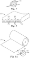
- a high density connector cable 210 is shown in FIG. 2 .
- the cable 210 which may for example be used as a connector cable for high speed data transfer applications, includes a plurality of metal signal conductors 212 that span the length of the cable 210, the conductors 212 being embedded in, and held in place by, a flexible insulator 214 such as a low dielectric loss polymer.
- the conductors 212 may be configured as differential pairs for data transfer, or in any other desired way. Although twelve conductors 212 are shown and arranged in two rows of six, fewer or greater than twelve conductors can be used, and they can be arranged in different numbers of rows and columns. In one such alternative embodiment, the cable may have only one conductor, or only two conductors.
- each of the conductors 212 is surrounded by an EMI shielding layer 220, where it is understood that the shielding layers 220 are made of the composite material 120.
- the shielding layers 220 may for example be extruded through a die during the fabrication of the cable 210.
- the shielding layers 220 are shown as completely surrounding their respective conductors 212, but in alternative embodiments a given shielding layer may surround a set of two or more conductors, and in still other embodiments the shielding layers may only partially surround one, two, or more of the conductors.
- the partial surrounding may be realized, for example, by an EMI shielding layer that, in perpendicular cross-section, spans a given row of two or three conductors or more, but that undulates periodically in a v-shape between adjacent conductors 212 so as to partially surround each conductor.
- a flexible EMI shielding film 310 is shown in FIG. 3A .
- the film 310 includes an EMI shielding layer 320, and an optional layer 324.
- the EMI shielding layer 320 is made of a composite material that may be the same as or similar to composite material 120, and thus is shown as having ceramic particles 322 dispersed in a matrix material 321, the ceramic particles 322 assumed to comprise TiO.
- the film 310 and the layer 320 have respective thicknesses and material compositions that allow them to flex, hence, the film 310 is flexible and is shown wound up into a film roll.
- the optional layer 324 may be omitted such that the film 310 is made up of only the EMI shielding layer 320. In other embodiments, the optional layer 324 may be included.
- the optional layer 324 attaches to the shielding layer 320 and may, for example, be or comprise a carrier film that carries the EMI shielding layer 320, or an adhesive layer, or a release liner.
- the optional layer 324 is typically made of another polymer material, but alternative materials may also be used.
- the film 310 may include additional layers of polymers or other materials.
- the flexible EMI shielding film 310 may be used as a tape from which one or more pieces can be cut and adhered to a workpiece such as a circuit, circuit component, or enclosure containing such a circuit or circuit component, for purposes of mitigating EMI.
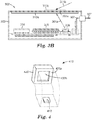
- FIG. 3B shows a schematic view of an enclosure 303 of a microelectronic board to which an EMI shielding film (or films) such as that of FIG. 3A has been applied.
- the enclosure 303 houses a circuit that includes some integrated circuits (ICs) 304, 306 and a large scale integrated circuit (LSI) 305, coupled to each other via a circuit board.
- ICs integrated circuits
- LSI large scale integrated circuit
- the enclosure 303 may be made of any suitable material, e.g. a thick metal to shield EMI by reflection. However, the enclosure has an aperture 303a which can allow EMI from the circuit to radiate outwardly (see arrow 301a ), and can also allow EMI originating from external sources to enter the enclosure 303 and disrupt the circuit (see arrow 301b ).
- a first EMI shielding film 310a and/or a second EMI shielding film 310b can be applied to the enclosure 303 to cover the aperture 303a.
- the shielding films 310a, 310b may be the same as or similar to the EMI shielding film 310 discussed above. Furthermore, if both shielding films 310a, 310b are used, such films may be the same, or different.
- a system 410 includes an EMI shielding body 420 and an electronic circuit component 412.
- the component 412 may be attached to a circuit board or other substrate by any known means, e.g., by surface mount technology.
- the body 420 is sized and shaped to fit over the component 412.
- the body 420 has a lower surface 420a that is contoured to form a shallow cavity 420b which may mate with or otherwise receive the circuit component 412 when the body 420 is placed atop the component 412, as indicated in the figure.
- the body 420 may be formed in situ over the circuit component 412 by a molding process.
- the body 420 is made of a composite material that may be the same as or similar to composite material 120, and includes TiO ceramic particles. Due to the substantial dielectric loss of the composite material, the body 420 effectively absorbs or otherwise blocks EMI from external sources that may interfere with the operation of the circuit component 412, as well as EMI that may be emitted by the component 412.
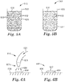
- a product 510 includes a container 502 that holds a printable ink 520.
- the ink 520 includes a solvent 521 within which are dispersed ceramic particles 522 and polymer particles 523.
- the ceramic particles 522 are made of or include TiO, and may be the same as or similar to the ceramic particles 122 discussed above.
- the polymer particles 523 are made of, or include, pieces of polymer material.
- the polymer material may be the same as or similar to any of the polymer materials discussed above in connection with the matrix material 121.
- the polymer material of the polymer particles 523 may be or include, for example, a fluorocarbon-based polymer, a chlorine-containing polymer, a (meth) acrylate polymer, silicone, an epoxy-based polymer, a polyether polymer, a copolymer thereof, or a combination thereof.
- the fluorocarbon-based polymer or copolymer may be or include a polyvinylidene fluoride (PVDF) polymer or copolymer, and/or a terpolymer of tetrafluoroethylene, hexafluoropropylene, and vinylidene fluoride.
- PVDF polyvinylidene fluoride
- the solvent 521 may be any suitable solvent, and in exemplary embodiments it is a liquid in which the polymer particles 523 can dissolve.
- Typical solvents include dimethylformamide (DMF), N-methyl-2-pyrrolidone (NMP), isopropanol (IPA), tetrahydrofuran (THF), benzene, and acetone, but these should not be considered as limiting.
- the ink 520 may also include other constituent components, such as one or more dyes and/or pigments to impart a desired color to the ink.
- the ink 520 may also include purely conductive particles such as any of those mentioned above in connection with the composite material 120.
- the ink may include suitable dispersants and surfactants for optimum dispersion of the fillers in the polymer solution.
- the ink 520 may be a precursor or intermediate product which then becomes a finished ink after the polymer particles have dissolved. Such a finished ink 520' is shown as a finished product 510' in FIG. 5B . Similar to FIG. 5A , the ink 520' is resident in the same container 502 and contains the same ceramic particles 522 as the precursor ink 520. In place of the solvent 521 and polymer particles 523 of FIG. 5A , the ink 520' contains a "syrup" or polymer solution 521', which may be a liquid mixture of the solvent 521 and polymer chains that originated from the (now dissolved) polymer particles 523.
- the inks of FIGS. 5A and 5B may be printed, coated, sprayed, or otherwise applied to a surface of interest such as a circuit, circuit component, container, film, substrate, or other workpiece of interest, and then dried to produce a finished (solid) composite material.
- concentration of the ceramic particles 522 in the original ink can be tailored so that the cured (dry or solid) composite material has a dielectric loss tangent of at least 0.15, or at least 0.2, or at least 0.3, or at least 0.4, over a range from 1 GHz to 5 GHz.
- the ceramic particles may make up a portion of the dry composite material, the portion being at least 10 vol. %, or at least 15 vol. % but no more than 60 vol. %, or at least 25 vol. % but no more than 50 vol. %.
- Figures 6A and 6B show how the inks can be applied to an electronic circuit component and then dried.
- a circuit component 604 mounted to a circuit board or other substrate 606 is positioned near a nozzle 601 at a printing station 610.
- the nozzle 601 connects to a supply of ink in liquid form such as ink 520 or ink 520', and dispenses the ink from an outlet 601a of the nozzle 601, the ink flowing through the nozzle and exiting the outlet as indicated by the arrows 620.
- the dispensed ink thus forms a liquid coating, film, or layer on the component 604.
- the dispensed ink forms a coating 620' atop the component 604 at a station 611, which may be the same as the coating station 610 or a separate drying station.
- the coating 620' in the figure represents the coated ink after drying and after removal of the solvent, but it may alternatively represent the coated ink while the ink is still wet before removal of the solvent. In either case, the coating 620' provides substantial EMI mitigation at high frequencies for the circuit component 604 or for any other workpiece to which it is applied.
- Item 1 is a composition comprising a composite material for mitigating electromagnetic interference (EMI), the composite material comprising: a matrix material; and ceramic particles dispersed within the matrix material; wherein the ceramic particles comprise titanium monoxide (TiO).
- EMI electromagnetic interference
- the composite material comprising: a matrix material; and ceramic particles dispersed within the matrix material; wherein the ceramic particles comprise titanium monoxide (TiO).
- Item 2 is the composition of item 1, wherein the composite material comprises from 10 vol. % to 60 vol. %, of the ceramic particles.
- Item 3 is the composition of any of the preceding items, wherein the composite material comprises from 15 vol. % to 60 vol. % of the ceramic particles.
- Item 4 is the composition of any of the preceding items, wherein the composite material comprises from 25 % to 50 vol. % of the ceramic particles.
- Item 5 is the composition of any preceding item, wherein the composite material has a dielectric loss tangent of at least 0.15.
- Item 6 is the composition of any preceding item, wherein the composite material has a dielectric loss tangent of at least 0.2.
- Item 7 is the composition of any preceding item, wherein the composite material has a dielectric loss tangent of at least 0.3.
- Item 8 is the composition of any preceding item, wherein the composite material has a dielectric loss tangent of at least 0.4.
- Item 9 is the composition of any of items 4 to 7, wherein the dielectric loss tangent has a first loss tangent component due to the ceramic particles and a second loss tangent component due to the matrix material, and wherein the first loss tangent component is at least 0.1.
- Item 10 is the composition of any of items 4 to 8, wherein the dielectric loss tangent has a first loss tangent component due to the ceramic particles and a second loss tangent component due to the matrix material, and wherein the first loss tangent component is at least 0.2.
- Item 11 is the composition of any of items 4 to 9, wherein the dielectric loss tangent has a first loss tangent component due to the ceramic particles and a second loss tangent component due to the matrix material, and wherein the first loss tangent component is at least 0.3.
- Item 12 is the composition of any of items 4 to 10, wherein the second loss tangent component is at least 0.01.
- Item 13 is the composition of any of items 4 to 11, wherein the second loss tangent component is at least 0.05.
- Item 14 is the composition of any of items 4 to 12, wherein the dielectric loss tangent has a first loss tangent component due to the ceramic particles and a second loss tangent component due to the matrix material, and wherein the second loss tangent component is at least
- Item 15 is the composition of any of items 4 to 14, wherein the dielectric loss tangent is over a range from 1 GHz to 60 GHz.
- Item 16 is the composition of any of items 4 to 15, wherein the dielectric loss tangent is over a range from 1 GHz to 25 GHz,
- Item 17 is the composition of any of items 4 to 16, wherein the dielectric loss tangent is over a range from 1 GHz to 15 GHz.
- Item 18 is the composition of any of items 4 to 16, wherein the dielectric loss tangent is over a range from 1 GHz to 10 GHz.
- Item 19 is the composition of any of items 4 to 16, wherein the dielectric loss tangent is over a range from 1 GHz to 5 GHz.
- Item 20 is the composition of any of the preceding items, further comprising one or more additional components.
- Item 21 is the composition of any of the preceeding items, wherein the one or more additional components include at least one of magnetic materials and conductive materials.
- Item 22 is the composition of any of titems 20-21, wherein one or more additional components include at least one of nanosilica, carbonyl iron, Ba 3 Co 3 Fe 24 O 41 , Y 3 Fe 5 O 12 , and colloidal silica.
- Item 23 is a composition of item 22, wherein the nanosilica is hydrophobic nanosilica.
- Item 24 is a composition of item 22, wherein one or more additional components include carbonyl iron.
- Item 25 is a composition of item 22, wherein one or more additional components include Ba 3 Co 3 Fe 24 O 41 .
- Item 26 is a composition of item 22, wherein one or more additional components include Y 3 Fe 5 O 12 .
- Item 27 is a composition of item 22, wherein one or more additional components include colloidal silica.
- Item 28 is the composition of any preceding item, wherein the matrix material comprises a polymeric matrix material.
- Item 29 is the composition of item 28, wherein the polymeric matrix material comprises a fluorocarbon-based polymer, a chlorine-containing polymer, a (meth) acrylate polymer, silicone, an epoxy-based polymer, a polyether polymer, a copolymer thereof, or a combination thereof.
- the polymeric matrix material comprises a fluorocarbon-based polymer, a chlorine-containing polymer, a (meth) acrylate polymer, silicone, an epoxy-based polymer, a polyether polymer, a copolymer thereof, or a combination thereof.
- Item 30 is the composition of item 28, wherein the polymeric matrix material comprises a fluorocarbon-based polymer or copolymer.
- Item 31 is the composition of item 30, wherein the fluorocarbon-based polymer or copolymer comprises a polyvinylidene fluoride polymer or copolymer.
- Item 32 is the composition of item 30, wherein the fluorocarbon-based polymer or copolymer comprises a terpolymer of tetrafluoroethylene, hexafluoropropylene, and vinylidene fluoride.
- Item 33 is the composition of any preceding item, wherein the composition is present as an EMI shielding layer that at least partially surrounds one or more conductive lines of a cable comprising the one or more conductive lines
- Item 34 is the composition of any preceding item, wherein the composition is present as a component of a flexible EMI shielding layer.
- Item 35 is the composition of item 33, further comprising a film for carrying the EMI shielding layer.
- Item 36 is a composition of any preceding item, wherein the composition is in the form of a rigid body having a contoured shape.
- Item 37 is a composition of any of the preceding items in the form of an ink for mitigating electromagnetic interference that is adapted for printing on a workpiece.
- Item 38 is a composition of item 36, wherein the matrix material comprises a polymer and wherein the matrix material is present in a solvent.
- Item 39 a composition of item 38, wherein the polymer comprises a fluorocarbon-based polymer or copolymer.
- Item 40 is a composition of item 39, wherein the fluorocarbon-based polymer or copolymer comprises a polyvinylidene fluoride polymer or copolymer.
- Item 41 is a composition any of items 38 to 40, wherein the ink is configured to produce, after the solvent is removed, a solid or cured composite material having the polymer as a matrix material and the ceramic particles dispersed in the matrix material, the solid composite material, cured composite material, or cured solid composite material having a dielectric loss tangent of at least 0.15 over a range from 1 GHz to 25 GHz.
- Item 42 is composition of item 41, wherein the solid or cured composite material comprises at least 10 vol. % ceramic particles.
- Item 43 is a composition of any of the preceding items, wherein the composition has a magnetic loss tangent of at least 0.01.
- Item 44 is a composition of any of the preceding items, wherein the composition has a magnetic loss tangent of at least 0.03.
- Item 45 is a composition of any of the preceding items, wherein the composition has a magnetic loss tangent of at least 0.05.
- Item 46 is a composition of any of the preceding items, wherein the composition has a combined dielectric and magnetic loss tangent of at least 0.01.
- Item 47 is a composition of any of the preceding items, wherein the composition has a combined dielectric and magnetic loss tangent of at least 0.03.
- Item 48 is a composition of any of the preceding items, wherein the composition has a combined dielectric and magnetic loss tangent of at least 0.05.
- Item 49 is a composition of any of the preceding items, wherein the composition is a component of a notch filter for EMI suppression.
- Item 50 is a method of shielding an electronic device from electromagnetic interference, comprising: providing an electronic device; and placing article composition of any of the preceding claims in proximity to the electronic device.
- Item 50a is the method of item 50, wherein the placing comprises forming an EMI shielding article in situ proximate the electronic device.
- Item 51 is the method of item 50, wherein the placing comprises providing an ink and applying the ink in proximity to the electronic device.
- Item 52 is the method of item 51, wherein the applying the ink comprises coating the electronic device with the ink.
- Item 53 is the method of item 51, wherein the placing comprises providing an EMI shielding tape and taking a piece from the EMI shielding tape for use as the EMI shielding article.
- Item 54 is the method of item 49, wherein the placing comprises adhering the EMI shielding article to the electronic device.
- Item 55 is the method of item 49, wherein the placing comprises covering the electronic device with the EMI shielding article.
- Item 56 is the method of item 49, wherein the placing comprises at least partially surrounding the electronic device with the EMI shielding article in at least one cross-sectional plane.
- Item 57 is the method of item 56, wherein the placing comprises completely surrounding the electronic device with the EMI shielding article in the at least one cross-sectional plane.
- Item 58 is the method of item 49, wherein the composite material further comprises at least one of one or more dyes and one or more pigments.
- Item 59 is the method of any of items 49 to 58, wherein the composite material further comprises at least one conductive particle.
- Item 60 is the method of item 59, wherein the conductive particles comprise one or more of metal particles, metal alloy particles, carbon fibers, carbon bubbles and carbon foams, carbon nanotubes, metal nanoparticles, metal nanowires, graphite, graphene-based materials (including exfoliated graphite nanoplatelets, doped and undoped graphene, graphene nanoplatelets, reduced graphene oxide, functionalized graphene sheets, and combinations thereof), and insulating particles with conductive coatings.
- the conductive particles comprise one or more of metal particles, metal alloy particles, carbon fibers, carbon bubbles and carbon foams, carbon nanotubes, metal nanoparticles, metal nanowires, graphite, graphene-based materials (including exfoliated graphite nanoplatelets, doped and undoped graphene, graphene nanoplatelets, reduced graphene oxide, functionalized graphene sheets, and combinations thereof), and insulating particles with conductive coatings.
- Item 61 is the method of any of items 49 to 60, wherein the electronic device comprises one or more electronic circuits and/or one or more electronic circuit components.
- Item 62 is the method of item 61, wherein the electronic device comprises an electronic circuit component, and the electronic circuit component comprises one or more integrated circuits (ICs), large scale integrated circuits (LSIs), processors, coprocessors, memory devices, transistors, resistors, capacitors, inductors, transmission lines, and/or conductors.
- ICs integrated circuits
- LSIs large scale integrated circuits
- processors coprocessors
- memory devices transistors, resistors, capacitors, inductors, transmission lines, and/or conductors.
- Item 563 is an article or system produced by the method of any of the items 49 to 62.
- % solvent blend of ethanol:methanol which were added to a 500 mL 3-neck round bottom flask (Ace Glass, Vineland, N.J.). The flask containing the mixture was placed in an oil bath set at 80° C with stirring for 4 hours to prepare hydrophobically modified nanosilica particles. The hydrophobically modified nanosilica particles were transferred to a crystallizing dish and dried in a convection oven at 150° C for 2 hours.
- Example 1 Composites with wax matrix material and dielectrically lossy TiO fillers
- As-received TiO powders were ground manually in a mortar and pestle to eliminate any large agglomerates.
- a stoichiometric amount of the TiO powder was dry mixed with a wax mixture (a blend of CALWAX 8345 and paraffin at 4:1 wt. ratio, respectively) in a SPEEDMIXER (Model DAC 150.1 FVZ, obtained from FlacTek Inc., Landrum, SC).
- the resulting mixture was placed in an oven pre-set at 150°C for 10 minutes. Once the wax was molten, the mix was then poured into an aluminum weighing pan. Once the mold was cold and hardened into a solid, a pellet of the resulting composite material was taken out.
- the amount of TiO in the composite was about 57.8 wt. %, which corresponds to about 20 vol. % loading.
- the composite pellet was then cut into a toroidal body for dielectric co-axial measurements.
- the toroidal body had an outer diameter of 2.54 cm, an inner diameter of 1.10 cm, and a thickness (or height or length) of 3 to 4 mm.
- Complex dielectric properties were calculated over the GHz frequency range using an Agilent E8363C Network Analyzer (obtained from Agilent Technologies, Santa Clara, CA) coupled to a Damaskos Model 100T Air Coaxial test fixture (obtained from Damaskos Inc., Concordville, PA).
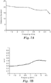
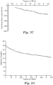
- the dielectric constant (D k ) of the TiO/wax composites ranged from about 20-21 at low gigahertz frequencies (e.g. 1-2 GHz) to about 15 at higher gigahertz frequencies (e.g. 5 GHz), as shown in FIG. 7A .
- the Example 1 sample exhibited a dielectric loss tangent (tan d) of about 0.3 at 1 GHz, and about 0.5 at 5 GHz, as shown in FIG. 7B .
- a dielectric loss tangent is high enough to be useful for shielding and absorbing materials as it pertains to EMI.
- the dielectric loss tangent of the paraffin wax by itself, with no TiO filler was about 0.002 -0.005 over the same gigahertz frequency range. Thus, the TiO filler is almost solely responsible for the high dielectric loss tangent of the composite material as shown in FIG. 7B .
- the traveling wave loss versus frequency was measured for the same Example 1 sample using the same dielectric measurement technique described earlier, and the results are shown in FIG. 7C .
- the results demonstrate that the composite material of this Example can decrease EMI interference waves at the frequencies shown.
- Example 2 Composites with PVDF matrix material and dielectrically lossy TiO fillers
- the hot-pressed composite was then allowed to cool down to room temperature where it hardened into a solid, and was then cut into a toroidal body having an outer diameter of 2.54 cm, an inner diameter of 1.10 cm, and a thickness (or height or length) of 2 to 3 mm.
- the amount of TiO in the composite was about 54.09 wt. %, which corresponds to about 30 vol. % loading.
- Complex dielectric properties were calculated over the GHz frequency range using an Agilent E8363C Network Analyzer coupled to a Damaskos Model 100T Air Coaxial test fixture.
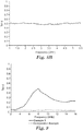
- Figures 8A and 8B show the measured dielectric response of the Example 2 TiO / PVDF composite material from 1GHz to 5.5 GHz.
- the base polymer PVDF by itself, with no TiO filler, has a dielectric constant (D k ) of about 3.0 over the measured frequency range (from 1 GHz to 5.5 GHz) and has a dielectric loss tangent (tan d) of about 0.1 to 0.08 over the same gigahertz frequency range.
- Example 3 Composites with epoxy matrix material and dielectrically lossy TiO fillers
- a toroid i.e., a doughnut
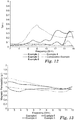
- Figure 9 shows the measured dielectric response tan of the Example 3 and Comparative Example A composite material from 2GHz to 16 GHz.
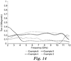
- the dielectric constant, tan , magnetic permeability and tan (magnetic) of Example 3 are compared to those of other Examples in Figures 11-14 .
- Example 4 Composites with epoxy matrix material and TiO -YIG fillers
- Example 4 The dielectric constant, tan , magnetic permeability and tan (magnetic) of Example 4 are compared to those of other Examples in Figures 11-14 .
- Example 5 Composites with epoxy matrix material and TiO -CIPfillers
- Example 5 samples were prepared in the same manner as Example 4 samples except that 20 g of CIP powders were used instead of 20 g of YIG powders to make the filler materials.
- Figure 10 shows the measured dielectric response tan of the Example 5 and Comparative Example A composite material from 2GHz to 18 GHz.
- the dielectric constant, tan , magnetic permeability and tan (magnetic) of Example 5 are compared to those of other Examples in Figures 11-14 .
- Example 6 Composites with epoxy matrix material and TiO -Co 2 Zferrite fillers
- Example 6 samples were prepared in the same manner as Example 4 samples except that 20 g of Co 2 Z ferrite powders were used instead of 20 g of YIG powders to make the filler materials.
- Example 3 The dielectric constant, tan , magnetic permeability and tan (magnetic) of Example 3 are compared to those of other Examples in Figures 11-14 ..
Claims (15)
- Eine Zusammensetzung, die ein Verbundmaterial (120) zur Verringerung der elektromagnetischen Interferenz (EMI) umfasst, wobei das Verbundmaterial (120) Folgendes umfasst: ein Matrixmaterial (121); und Keramikteilchen (122), die in dem Matrixmaterial (121) dispergiert sind; dadurch gekennzeichnet, dass die Keramikteilchen (122) Titanmonoxid (TiO) umfassen.
- Die Zusammensetzung nach Anspruch 1, wobei das Verbundmaterial von 10 Vol.-% bis 60 Vol.-% der Teilchen umfasst.
- Die Zusammensetzung nach einem der vorstehenden Ansprüche, wobei das Verbundmaterial eine dielektrische Verlusttangente von mindestens 0,15 aufweist.
- Die Zusammensetzung nach einem der vorstehenden Ansprüche, wobei die dielektrische Verlusttangente eine erste Verlusttangentenkomponente aufgrund der Keramikteilchen und eine zweite Verlusttangentenkomponente aufgrund des Matrixmaterials aufweist, und wobei die erste Verlusttangentenkomponente mindestens 0,1 ist.
- Die Zusammensetzung nach Anspruch 4, wobei die zweite Verlusttangentenkomponente mindestens 0,01 ist.
- Die Zusammensetzung nach einem der vorstehenden Ansprüche, wobei die dielektrische Verlusttangente über einen Bereich von 1 GHz bis 60 GHz beträgt.
- Die Zusammensetzung nach einem der vorstehenden Ansprüche, ferner umfassend eine oder mehrere zusätzliche Komponenten.
- Die Zusammensetzung nach einem der vorstehenden Ansprüche, wobei eine oder mehrere zusätzliche Komponenten mindestens eines von Nanosiliciumdioxid, Carbonyleisen, Ba3Co3Fe24O41, Carbonyleisen und Y3Fe5O12 einschließt.
- Die Zusammensetzung nach einem der vorstehenden Ansprüche, wobei das Matrixmaterial ein Polymermatrixmaterial umfasst.
- Die Zusammensetzung nach einem der vorstehenden Ansprüche, wobei das Verbundmaterial eine dielektrische Verlusttangente von mindestens 0,03 aufweist.
- Die Zusammensetzung nach einem der vorstehenden Ansprüche, wobei das Verbundmaterial eine magnetische Verlusttangente von mindestens 0,03 aufweist.
- Die Zusammensetzung nach einem der vorstehenden Ansprüche, wobei das Verbundmaterial eine Kombination aus dielektrischer und magnetischer Verlusttangente von mindestens 0,03 aufweist.
- Die Zusammensetzung nach einem der vorstehenden Ansprüche, wobei die Zusammensetzung eine Komponente eines Kerbfilters zur EMI-Unterdrückung ist.
- Die Zusammensetzung nach einem der vorstehenden Ansprüche, wobei die Zusammensetzung als eine Komponente einer flexiblen EMI-Abschirmschicht vorhanden ist.
- Die Zusammensetzung nach einem der vorstehenden Ansprüche, wobei die Zusammensetzung als eine Komponente einer EMI-Abschirmschicht vorhanden ist, die eine oder mehrere Leiterbahnen eines Kabels, das die eine oder die mehreren Leiterbahnen umfasst, mindestens teilweise umgibt.
Applications Claiming Priority (3)
| Application Number | Priority Date | Filing Date | Title |
|---|---|---|---|
| US201361917661P | 2013-12-18 | 2013-12-18 | |
| US201461985124P | 2014-04-28 | 2014-04-28 | |
| PCT/US2014/069787 WO2015094915A1 (en) | 2013-12-18 | 2014-12-11 | Electromagnetic interference (emi) shielding products using titanium monoxide (tio) based materials |
Publications (2)
| Publication Number | Publication Date |
|---|---|
| EP3085215A1 EP3085215A1 (de) | 2016-10-26 |
| EP3085215B1 true EP3085215B1 (de) | 2019-09-04 |
Family
ID=52347407
Family Applications (1)
| Application Number | Title | Priority Date | Filing Date |
|---|---|---|---|
| EP14827314.7A Active EP3085215B1 (de) | 2013-12-18 | 2014-12-11 | Abschirmungsprodukte für elektromagnetische interferenz (emi) unter verwendung von material auf der basis von titanmonoxid (tio) |
Country Status (5)
| Country | Link |
|---|---|
| US (1) | US10932398B2 (de) |
| EP (1) | EP3085215B1 (de) |
| JP (1) | JP2017502513A (de) |
| CN (1) | CN105814979B (de) |
| WO (1) | WO2015094915A1 (de) |
Families Citing this family (13)
| Publication number | Priority date | Publication date | Assignee | Title |
|---|---|---|---|---|
| FR3019179B1 (fr) * | 2014-03-28 | 2017-11-24 | Saint Gobain Ct Recherches | Composites polymere-ceramique |
| EP3308614B1 (de) | 2015-06-09 | 2020-08-19 | 3M Innovative Properties Company | Verbundstoffe gegen hochfrequenter elektromagnetische interferenz (emi) |
| US9807866B2 (en) * | 2015-11-30 | 2017-10-31 | Intel Corporation | Shielding mold for electric and magnetic EMI mitigation |
| WO2017116656A1 (en) | 2015-12-29 | 2017-07-06 | 3M Innovative Properties Company | Composites for high frequency electromagnetic interference (emi) applications |
| US9820418B1 (en) * | 2016-03-24 | 2017-11-14 | Jose Machado | Electromagnetic contamination neutralization composition, device, and method |
| WO2019161282A1 (en) * | 2018-02-17 | 2019-08-22 | Laird Technologies, Inc. | Thermal interface materials having high dielectric losses and low dielectric constants |
| WO2019193528A1 (en) | 2018-04-06 | 2019-10-10 | 3M Innovative Properties Company | Radar standing wave dampnening components and systems |
| CN112585541A (zh) * | 2018-08-21 | 2021-03-30 | 莱尔德技术股份有限公司 | 图案化材料和膜以及用于制备其的系统和方法 |
| US11512180B2 (en) | 2018-11-14 | 2022-11-29 | Eden Innovations Ltd. | Method for fabricating carbon nanoparticle polymer matrix composites using electromagnetic irradiation |
| CN110157346B (zh) * | 2019-05-06 | 2021-05-07 | 费植煌 | 一种含石墨烯的装饰膜 |
| TWI744800B (zh) * | 2020-02-13 | 2021-11-01 | 國立高雄科技大學 | 船舶電纜電磁干擾屏蔽改善分析系統 |
| CN113772957B (zh) * | 2021-08-17 | 2023-03-21 | 浙江理工大学 | 一种用于磁控超疏水表面构筑的改性羰基铁粉制备及其在蓝光固化超疏水薄膜中的应用 |
| KR102594352B1 (ko) * | 2022-10-13 | 2023-10-26 | 주식회사 유라 | 전자파 차폐성능이 개선된 자동차용 고속통신 케이블 및 이의 제조방법 |
Citations (1)
| Publication number | Priority date | Publication date | Assignee | Title |
|---|---|---|---|---|
| EP2505618A1 (de) * | 2011-04-01 | 2012-10-03 | Fábrica Nacional De Moneda Y Timbre | Verwendung der elektromagnetische Strahlung absorbierenden Markierungsstoffe zur Sicherheitskennzeichnung |
Family Cites Families (36)
| Publication number | Priority date | Publication date | Assignee | Title |
|---|---|---|---|---|
| US3671275A (en) | 1969-12-12 | 1972-06-20 | Hughes Aircraft Co | Lossy dielectric structure for dissipating electrical microwave energy |
| US4568603A (en) | 1984-05-11 | 1986-02-04 | Oldham Susan L | Fiber-reinforced syntactic foam composites prepared from polyglycidyl aromatic amine and polycarboxylic acid anhydride |
| US5019681A (en) * | 1990-02-14 | 1991-05-28 | The Pillsbury Company | Reflective temperature compensating microwave susceptors |
| JPH04130682A (ja) * | 1990-09-20 | 1992-05-01 | Mitsubishi Kasei Corp | アクチュエータ用圧電セラミック組成物 |
| CA2060709C (en) * | 1991-02-08 | 1996-06-04 | Kiyotaka Komori | Glass fiber forming composition, glass fibers obtained from the composition and substrate for circuit board including the glass fibers as reinforcing material |
| US5691498A (en) | 1992-02-07 | 1997-11-25 | Trw Inc. | Hermetically-sealed electrically-absorptive low-pass radio frequency filters and electromagnetically lossy ceramic materials for said filters |
| US20010051286A1 (en) * | 1996-02-07 | 2001-12-13 | Shigeto Oiri | Magnetic recording medium having a magnetic layer and a coating thereunder |
| US6753277B2 (en) * | 2000-02-29 | 2004-06-22 | Kyocera Corporation | Ceramics having excellent high-frequency characteristics and method of producing the same |
| JP2001330985A (ja) * | 2000-05-22 | 2001-11-30 | Fuji Xerox Co Ltd | トリクル現像方式用現像剤及び画像形成方法 |
| JP4115682B2 (ja) * | 2000-05-25 | 2008-07-09 | 日本碍子株式会社 | 金属間化合物基複合材料の製造方法 |
| JP3639773B2 (ja) * | 2000-06-19 | 2005-04-20 | キヤノン株式会社 | 半導電性ゴム組成物、帯電部材、電子写真装置、プロセスカートリッジ |
| KR20050093808A (ko) * | 2002-12-27 | 2005-09-23 | 티디케이가부시기가이샤 | 수지조성물, 수지경화물, 시트형상 수지경화물, 적층체,프리프레그, 전자부품 및 다층기판 |
| US7149466B2 (en) * | 2004-02-12 | 2006-12-12 | Sumitomo Rubber Industries, Ltd. | Conductive rubber member |
| CN1926933B (zh) * | 2004-03-01 | 2010-12-08 | 新田株式会社 | 电磁波吸收体 |
| CN101390253B (zh) * | 2004-10-01 | 2013-02-27 | L.皮尔·德罗什蒙 | 陶瓷天线模块及其制造方法 |
| US20070267603A1 (en) * | 2004-12-17 | 2007-11-22 | Kazuhisa Takagi | Method of Controlling Specific Inductive Capacity, Dielectric Material, Mobil Phone and Human Phantom Model |
| US8007976B2 (en) * | 2005-11-02 | 2011-08-30 | Ricoh Company. Ltd. | Electrostatic image developing toner, toner kit and image forming apparatus |
| US20090010187A1 (en) * | 2007-07-06 | 2009-01-08 | Somesh Agarwal | System and Method for an Adaptive Access Point Mode |
| CN101755241B (zh) * | 2007-07-19 | 2012-09-19 | 佳能株式会社 | 非磁性调色剂 |
| US7815820B2 (en) | 2007-10-18 | 2010-10-19 | General Electric Company | Electromagnetic interference shielding polymer composites and methods of manufacture |
| TWI405801B (zh) | 2007-10-19 | 2013-08-21 | Nat Univ Tsing Hua | 具有電磁波干擾遮蔽效應之多壁碳奈米管/高分子奈米複合材之製備方法 |
| WO2010027074A1 (ja) * | 2008-09-05 | 2010-03-11 | 住友電気工業株式会社 | セラミックス粉末、該セラミックス粉末を含有する誘電性複合材料、及び誘電体アンテナ |
| JP4681039B2 (ja) * | 2008-12-04 | 2011-05-11 | 住友ゴム工業株式会社 | 導電性ロール |
| US8138429B2 (en) | 2008-12-17 | 2012-03-20 | 3M Innovative Properties Company | Electromagnetic shielding article |
| JP2011018873A (ja) | 2009-05-22 | 2011-01-27 | Sony Ericsson Mobilecommunications Japan Inc | 電磁シールド方法および電磁シールド用フィルム |
| BR112012000203B1 (pt) | 2009-06-12 | 2020-01-28 | Lord Corp | método para proteção de um substrato contra relâmpagos |
| EP2659757A2 (de) | 2010-12-28 | 2013-11-06 | Saint-gobain Performance Plastics Corporation | Polymere mit einem metallfüllstoff zur emi-abschirmung |
| US8772188B2 (en) * | 2012-03-12 | 2014-07-08 | Schott Ag | Glass-ceramic having at least two crystal phases, process for producing a glass-ceramic and its use |
| JP5701807B2 (ja) * | 2012-03-29 | 2015-04-15 | 株式会社東芝 | 圧力センサ及びマイクロフォン |
| US9916998B2 (en) * | 2012-12-04 | 2018-03-13 | Applied Materials, Inc. | Substrate support assembly having a plasma resistant protective layer |
| US9685356B2 (en) * | 2012-12-11 | 2017-06-20 | Applied Materials, Inc. | Substrate support assembly having metal bonded protective layer |
| US9894750B2 (en) | 2012-12-20 | 2018-02-13 | 3M Innovative Properties Company | Floating connector shield |
| US9704613B2 (en) | 2013-02-21 | 2017-07-11 | 3M Innovative Properties Company | Polymer composites with electromagnetic interference mitigation properties |
| JP5822146B2 (ja) * | 2013-03-29 | 2015-11-24 | パウダーテック株式会社 | ノイズ抑制用複合磁性粉 |
| JP6320206B2 (ja) * | 2014-07-07 | 2018-05-09 | キヤノン株式会社 | 印刷システム、画像処理装置、情報処理方法及びプログラム |
| GB2550738B (en) * | 2015-03-19 | 2021-08-18 | Rogers Corp | Magneto-dielectric substrate, circuit material, and assembly having the same |
-
2014
- 2014-12-11 WO PCT/US2014/069787 patent/WO2015094915A1/en active Application Filing
- 2014-12-11 JP JP2016541289A patent/JP2017502513A/ja not_active Withdrawn
- 2014-12-11 US US15/102,863 patent/US10932398B2/en active Active
- 2014-12-11 CN CN201480068141.5A patent/CN105814979B/zh active Active
- 2014-12-11 EP EP14827314.7A patent/EP3085215B1/de active Active
Patent Citations (1)
| Publication number | Priority date | Publication date | Assignee | Title |
|---|---|---|---|---|
| EP2505618A1 (de) * | 2011-04-01 | 2012-10-03 | Fábrica Nacional De Moneda Y Timbre | Verwendung der elektromagnetische Strahlung absorbierenden Markierungsstoffe zur Sicherheitskennzeichnung |
Also Published As
| Publication number | Publication date |
|---|---|
| EP3085215A1 (de) | 2016-10-26 |
| US10932398B2 (en) | 2021-02-23 |
| CN105814979B (zh) | 2020-01-10 |
| CN105814979A (zh) | 2016-07-27 |
| JP2017502513A (ja) | 2017-01-19 |
| US20160309628A1 (en) | 2016-10-20 |
| WO2015094915A1 (en) | 2015-06-25 |
Similar Documents
| Publication | Publication Date | Title |
|---|---|---|
| EP3085215B1 (de) | Abschirmungsprodukte für elektromagnetische interferenz (emi) unter verwendung von material auf der basis von titanmonoxid (tio) | |
| Xiang et al. | Facile synthesis and enhanced microwave absorption properties of multiferroic Ni0. 4Co0. 2Zn0. 4Fe2O4/BaTiO3 composite fibers | |
| TW566077B (en) | Electromagnetic wave absorption material and an associated device | |
| Peng et al. | Microwave absorbing materials using Ag–NiZn ferrite core–shell nanopowders as fillers | |
| Olad et al. | Electromagnetic interference attenuation and shielding effect of quaternary Epoxy-PPy/Fe3O4-ZnO nanocomposite as a broad band microwave-absorber | |
| Cheng et al. | Electromagnetic and microwave absorption properties of carbonyl iron/La0. 6Sr0. 4MnO3 composites | |
| JP4417377B2 (ja) | 電磁波ノイズ抑制体、電磁波ノイズ抑制機能付構造体、およびそれらの製造方法 | |
| US20100311866A1 (en) | Heirarchial polymer-based nanocomposites for emi shielding | |
| EP3029771B1 (de) | Absorber für elektromagnetische wellen und filmbildende paste | |
| US20170288305A1 (en) | High-frequency antenna element and high-frequency antenna module | |
| US20200053920A1 (en) | High-dielectric-loss composites for electromagnetic interference (emi) applications | |
| JP2008021990A (ja) | 電磁干渉抑制体および電磁障害抑制方法 | |
| KR101385823B1 (ko) | 전자파 간섭 억제 시트, 고주파 신호용 플랫 케이블, 연성 인쇄 기판 및 전자파 간섭 억제 시트의 제조 방법 | |
| EP3308614B1 (de) | Verbundstoffe gegen hochfrequenter elektromagnetische interferenz (emi) | |
| Zhao et al. | Layered composites composed of multi-walled carbon nanotubes/manganese dioxide/carbon fiber cloth for microwave absorption in the X-band | |
| Yang et al. | Dielectric and microwave absorption properties of TiAlCo ceramic fabricated by atmospheric plasma spraying | |
| Jiang et al. | Electromagnetic wave absorption and dielectric-modulation of metallic perovskite lanthanum nickel oxide | |
| CN112205093A (zh) | 电波吸收层叠膜、其制造方法、以及包含其的元件 | |
| US20080006352A1 (en) | Magnetic sheet and method of producing the same | |
| US6063511A (en) | Low cost thin film magnetodielectric material | |
| Sasikumar et al. | Electromagnetic interference shielding efficiency enhancement of the PANI-CSA films at broad band frequencies | |
| KR100933371B1 (ko) | 유전체층의 기능이 부여된 연자성체층을 포함하는 전자파흡수체 및 그 연자성체층의 형성방법 | |
| KR102082810B1 (ko) | 고성능 복합 전자파 차폐시트 및 이의 제조방법 | |
| KR20090089277A (ko) | 유전체층의 기능이 부여된 연자성체층을 포함하는 전자파 흡수체 및 그 연자성체층의 형성방법 | |
| WO2022092137A1 (ja) | 電磁波吸収シート |
Legal Events
| Date | Code | Title | Description |
|---|---|---|---|
| PUAI | Public reference made under article 153(3) epc to a published international application that has entered the european phase |
Free format text: ORIGINAL CODE: 0009012 |
|
| 17P | Request for examination filed |
Effective date: 20160613 |
|
| AK | Designated contracting states |
Kind code of ref document: A1 Designated state(s): AL AT BE BG CH CY CZ DE DK EE ES FI FR GB GR HR HU IE IS IT LI LT LU LV MC MK MT NL NO PL PT RO RS SE SI SK SM TR |
|
| AX | Request for extension of the european patent |
Extension state: BA ME |
|
| DAX | Request for extension of the european patent (deleted) | ||
| STAA | Information on the status of an ep patent application or granted ep patent |
Free format text: STATUS: EXAMINATION IS IN PROGRESS |
|
| 17Q | First examination report despatched |
Effective date: 20181112 |
|
| GRAP | Despatch of communication of intention to grant a patent |
Free format text: ORIGINAL CODE: EPIDOSNIGR1 |
|
| STAA | Information on the status of an ep patent application or granted ep patent |
Free format text: STATUS: GRANT OF PATENT IS INTENDED |
|
| INTG | Intention to grant announced |
Effective date: 20190328 |
|
| GRAS | Grant fee paid |
Free format text: ORIGINAL CODE: EPIDOSNIGR3 |
|
| GRAA | (expected) grant |
Free format text: ORIGINAL CODE: 0009210 |
|
| STAA | Information on the status of an ep patent application or granted ep patent |
Free format text: STATUS: THE PATENT HAS BEEN GRANTED |
|
| AK | Designated contracting states |
Kind code of ref document: B1 Designated state(s): AL AT BE BG CH CY CZ DE DK EE ES FI FR GB GR HR HU IE IS IT LI LT LU LV MC MK MT NL NO PL PT RO RS SE SI SK SM TR |
|
| REG | Reference to a national code |
Ref country code: GB Ref legal event code: FG4D |
|
| REG | Reference to a national code |
Ref country code: CH Ref legal event code: EP |
|
| REG | Reference to a national code |
Ref country code: AT Ref legal event code: REF Ref document number: 1177276 Country of ref document: AT Kind code of ref document: T Effective date: 20190915 |
|
| REG | Reference to a national code |
Ref country code: DE Ref legal event code: R096 Ref document number: 602014053129 Country of ref document: DE |
|
| REG | Reference to a national code |
Ref country code: IE Ref legal event code: FG4D |
|
| REG | Reference to a national code |
Ref country code: NL Ref legal event code: MP Effective date: 20190904 |
|
| REG | Reference to a national code |
Ref country code: LT Ref legal event code: MG4D |
|
| PG25 | Lapsed in a contracting state [announced via postgrant information from national office to epo] |
Ref country code: NO Free format text: LAPSE BECAUSE OF FAILURE TO SUBMIT A TRANSLATION OF THE DESCRIPTION OR TO PAY THE FEE WITHIN THE PRESCRIBED TIME-LIMIT Effective date: 20191204 Ref country code: FI Free format text: LAPSE BECAUSE OF FAILURE TO SUBMIT A TRANSLATION OF THE DESCRIPTION OR TO PAY THE FEE WITHIN THE PRESCRIBED TIME-LIMIT Effective date: 20190904 Ref country code: HR Free format text: LAPSE BECAUSE OF FAILURE TO SUBMIT A TRANSLATION OF THE DESCRIPTION OR TO PAY THE FEE WITHIN THE PRESCRIBED TIME-LIMIT Effective date: 20190904 Ref country code: LT Free format text: LAPSE BECAUSE OF FAILURE TO SUBMIT A TRANSLATION OF THE DESCRIPTION OR TO PAY THE FEE WITHIN THE PRESCRIBED TIME-LIMIT Effective date: 20190904 Ref country code: BG Free format text: LAPSE BECAUSE OF FAILURE TO SUBMIT A TRANSLATION OF THE DESCRIPTION OR TO PAY THE FEE WITHIN THE PRESCRIBED TIME-LIMIT Effective date: 20191204 Ref country code: SE Free format text: LAPSE BECAUSE OF FAILURE TO SUBMIT A TRANSLATION OF THE DESCRIPTION OR TO PAY THE FEE WITHIN THE PRESCRIBED TIME-LIMIT Effective date: 20190904 |
|
| PG25 | Lapsed in a contracting state [announced via postgrant information from national office to epo] |
Ref country code: GR Free format text: LAPSE BECAUSE OF FAILURE TO SUBMIT A TRANSLATION OF THE DESCRIPTION OR TO PAY THE FEE WITHIN THE PRESCRIBED TIME-LIMIT Effective date: 20191205 Ref country code: LV Free format text: LAPSE BECAUSE OF FAILURE TO SUBMIT A TRANSLATION OF THE DESCRIPTION OR TO PAY THE FEE WITHIN THE PRESCRIBED TIME-LIMIT Effective date: 20190904 Ref country code: AL Free format text: LAPSE BECAUSE OF FAILURE TO SUBMIT A TRANSLATION OF THE DESCRIPTION OR TO PAY THE FEE WITHIN THE PRESCRIBED TIME-LIMIT Effective date: 20190904 Ref country code: RS Free format text: LAPSE BECAUSE OF FAILURE TO SUBMIT A TRANSLATION OF THE DESCRIPTION OR TO PAY THE FEE WITHIN THE PRESCRIBED TIME-LIMIT Effective date: 20190904 Ref country code: ES Free format text: LAPSE BECAUSE OF FAILURE TO SUBMIT A TRANSLATION OF THE DESCRIPTION OR TO PAY THE FEE WITHIN THE PRESCRIBED TIME-LIMIT Effective date: 20190904 |
|
| REG | Reference to a national code |
Ref country code: AT Ref legal event code: MK05 Ref document number: 1177276 Country of ref document: AT Kind code of ref document: T Effective date: 20190904 |
|
| PG25 | Lapsed in a contracting state [announced via postgrant information from national office to epo] |
Ref country code: RO Free format text: LAPSE BECAUSE OF FAILURE TO SUBMIT A TRANSLATION OF THE DESCRIPTION OR TO PAY THE FEE WITHIN THE PRESCRIBED TIME-LIMIT Effective date: 20190904 Ref country code: IT Free format text: LAPSE BECAUSE OF FAILURE TO SUBMIT A TRANSLATION OF THE DESCRIPTION OR TO PAY THE FEE WITHIN THE PRESCRIBED TIME-LIMIT Effective date: 20190904 Ref country code: PT Free format text: LAPSE BECAUSE OF FAILURE TO SUBMIT A TRANSLATION OF THE DESCRIPTION OR TO PAY THE FEE WITHIN THE PRESCRIBED TIME-LIMIT Effective date: 20200106 Ref country code: PL Free format text: LAPSE BECAUSE OF FAILURE TO SUBMIT A TRANSLATION OF THE DESCRIPTION OR TO PAY THE FEE WITHIN THE PRESCRIBED TIME-LIMIT Effective date: 20190904 Ref country code: NL Free format text: LAPSE BECAUSE OF FAILURE TO SUBMIT A TRANSLATION OF THE DESCRIPTION OR TO PAY THE FEE WITHIN THE PRESCRIBED TIME-LIMIT Effective date: 20190904 Ref country code: AT Free format text: LAPSE BECAUSE OF FAILURE TO SUBMIT A TRANSLATION OF THE DESCRIPTION OR TO PAY THE FEE WITHIN THE PRESCRIBED TIME-LIMIT Effective date: 20190904 Ref country code: EE Free format text: LAPSE BECAUSE OF FAILURE TO SUBMIT A TRANSLATION OF THE DESCRIPTION OR TO PAY THE FEE WITHIN THE PRESCRIBED TIME-LIMIT Effective date: 20190904 |
|
| PG25 | Lapsed in a contracting state [announced via postgrant information from national office to epo] |
Ref country code: CZ Free format text: LAPSE BECAUSE OF FAILURE TO SUBMIT A TRANSLATION OF THE DESCRIPTION OR TO PAY THE FEE WITHIN THE PRESCRIBED TIME-LIMIT Effective date: 20190904 Ref country code: SM Free format text: LAPSE BECAUSE OF FAILURE TO SUBMIT A TRANSLATION OF THE DESCRIPTION OR TO PAY THE FEE WITHIN THE PRESCRIBED TIME-LIMIT Effective date: 20190904 Ref country code: IS Free format text: LAPSE BECAUSE OF FAILURE TO SUBMIT A TRANSLATION OF THE DESCRIPTION OR TO PAY THE FEE WITHIN THE PRESCRIBED TIME-LIMIT Effective date: 20200224 Ref country code: SK Free format text: LAPSE BECAUSE OF FAILURE TO SUBMIT A TRANSLATION OF THE DESCRIPTION OR TO PAY THE FEE WITHIN THE PRESCRIBED TIME-LIMIT Effective date: 20190904 |
|
| REG | Reference to a national code |
Ref country code: DE Ref legal event code: R097 Ref document number: 602014053129 Country of ref document: DE |
|
| PLBE | No opposition filed within time limit |
Free format text: ORIGINAL CODE: 0009261 |
|
| STAA | Information on the status of an ep patent application or granted ep patent |
Free format text: STATUS: NO OPPOSITION FILED WITHIN TIME LIMIT |
|
| PG2D | Information on lapse in contracting state deleted |
Ref country code: IS |
|
| PG25 | Lapsed in a contracting state [announced via postgrant information from national office to epo] |
Ref country code: DK Free format text: LAPSE BECAUSE OF FAILURE TO SUBMIT A TRANSLATION OF THE DESCRIPTION OR TO PAY THE FEE WITHIN THE PRESCRIBED TIME-LIMIT Effective date: 20190904 Ref country code: IS Free format text: LAPSE BECAUSE OF FAILURE TO SUBMIT A TRANSLATION OF THE DESCRIPTION OR TO PAY THE FEE WITHIN THE PRESCRIBED TIME-LIMIT Effective date: 20200105 |
|
| REG | Reference to a national code |
Ref country code: CH Ref legal event code: PL |
|
| 26N | No opposition filed |
Effective date: 20200605 |
|
| REG | Reference to a national code |
Ref country code: BE Ref legal event code: MM Effective date: 20191231 |
|
| PG25 | Lapsed in a contracting state [announced via postgrant information from national office to epo] |
Ref country code: MC Free format text: LAPSE BECAUSE OF FAILURE TO SUBMIT A TRANSLATION OF THE DESCRIPTION OR TO PAY THE FEE WITHIN THE PRESCRIBED TIME-LIMIT Effective date: 20190904 Ref country code: SI Free format text: LAPSE BECAUSE OF FAILURE TO SUBMIT A TRANSLATION OF THE DESCRIPTION OR TO PAY THE FEE WITHIN THE PRESCRIBED TIME-LIMIT Effective date: 20190904 |
|
| GBPC | Gb: european patent ceased through non-payment of renewal fee |
Effective date: 20191211 |
|
| PG25 | Lapsed in a contracting state [announced via postgrant information from national office to epo] |
Ref country code: GB Free format text: LAPSE BECAUSE OF NON-PAYMENT OF DUE FEES Effective date: 20191211 Ref country code: LU Free format text: LAPSE BECAUSE OF NON-PAYMENT OF DUE FEES Effective date: 20191211 Ref country code: IE Free format text: LAPSE BECAUSE OF NON-PAYMENT OF DUE FEES Effective date: 20191211 Ref country code: FR Free format text: LAPSE BECAUSE OF NON-PAYMENT OF DUE FEES Effective date: 20191231 |
|
| PG25 | Lapsed in a contracting state [announced via postgrant information from national office to epo] |
Ref country code: BE Free format text: LAPSE BECAUSE OF NON-PAYMENT OF DUE FEES Effective date: 20191231 Ref country code: CH Free format text: LAPSE BECAUSE OF NON-PAYMENT OF DUE FEES Effective date: 20191231 Ref country code: LI Free format text: LAPSE BECAUSE OF NON-PAYMENT OF DUE FEES Effective date: 20191231 |
|
| PG25 | Lapsed in a contracting state [announced via postgrant information from national office to epo] |
Ref country code: CY Free format text: LAPSE BECAUSE OF FAILURE TO SUBMIT A TRANSLATION OF THE DESCRIPTION OR TO PAY THE FEE WITHIN THE PRESCRIBED TIME-LIMIT Effective date: 20190904 |
|
| PG25 | Lapsed in a contracting state [announced via postgrant information from national office to epo] |
Ref country code: MT Free format text: LAPSE BECAUSE OF FAILURE TO SUBMIT A TRANSLATION OF THE DESCRIPTION OR TO PAY THE FEE WITHIN THE PRESCRIBED TIME-LIMIT Effective date: 20190904 Ref country code: HU Free format text: LAPSE BECAUSE OF FAILURE TO SUBMIT A TRANSLATION OF THE DESCRIPTION OR TO PAY THE FEE WITHIN THE PRESCRIBED TIME-LIMIT; INVALID AB INITIO Effective date: 20141211 |
|
| PG25 | Lapsed in a contracting state [announced via postgrant information from national office to epo] |
Ref country code: TR Free format text: LAPSE BECAUSE OF FAILURE TO SUBMIT A TRANSLATION OF THE DESCRIPTION OR TO PAY THE FEE WITHIN THE PRESCRIBED TIME-LIMIT Effective date: 20190904 |
|
| PG25 | Lapsed in a contracting state [announced via postgrant information from national office to epo] |
Ref country code: MK Free format text: LAPSE BECAUSE OF FAILURE TO SUBMIT A TRANSLATION OF THE DESCRIPTION OR TO PAY THE FEE WITHIN THE PRESCRIBED TIME-LIMIT Effective date: 20190904 |
|
| PGFP | Annual fee paid to national office [announced via postgrant information from national office to epo] |
Ref country code: DE Payment date: 20231121 Year of fee payment: 10 |