EP3084034B1 - Reaktionskammer zum epitaktischen wachstum mit einer lade-/entladevorrichtung und reaktor - Google Patents
Reaktionskammer zum epitaktischen wachstum mit einer lade-/entladevorrichtung und reaktor Download PDFInfo
- Publication number
- EP3084034B1 EP3084034B1 EP14833165.5A EP14833165A EP3084034B1 EP 3084034 B1 EP3084034 B1 EP 3084034B1 EP 14833165 A EP14833165 A EP 14833165A EP 3084034 B1 EP3084034 B1 EP 3084034B1
- Authority
- EP
- European Patent Office
- Prior art keywords
- reaction chamber
- covering
- supporting element
- chamber according
- loading
- Prior art date
- Legal status (The legal status is an assumption and is not a legal conclusion. Google has not performed a legal analysis and makes no representation as to the accuracy of the status listed.)
- Active
Links
Images


Classifications
-
- C—CHEMISTRY; METALLURGY
- C30—CRYSTAL GROWTH
- C30B—SINGLE-CRYSTAL GROWTH; UNIDIRECTIONAL SOLIDIFICATION OF EUTECTIC MATERIAL OR UNIDIRECTIONAL DEMIXING OF EUTECTOID MATERIAL; REFINING BY ZONE-MELTING OF MATERIAL; PRODUCTION OF A HOMOGENEOUS POLYCRYSTALLINE MATERIAL WITH DEFINED STRUCTURE; SINGLE CRYSTALS OR HOMOGENEOUS POLYCRYSTALLINE MATERIAL WITH DEFINED STRUCTURE; AFTER-TREATMENT OF SINGLE CRYSTALS OR A HOMOGENEOUS POLYCRYSTALLINE MATERIAL WITH DEFINED STRUCTURE; APPARATUS THEREFOR
- C30B25/00—Single-crystal growth by chemical reaction of reactive gases, e.g. chemical vapour-deposition growth
- C30B25/02—Epitaxial-layer growth
- C30B25/12—Substrate holders or susceptors
-
- C—CHEMISTRY; METALLURGY
- C23—COATING METALLIC MATERIAL; COATING MATERIAL WITH METALLIC MATERIAL; CHEMICAL SURFACE TREATMENT; DIFFUSION TREATMENT OF METALLIC MATERIAL; COATING BY VACUUM EVAPORATION, BY SPUTTERING, BY ION IMPLANTATION OR BY CHEMICAL VAPOUR DEPOSITION, IN GENERAL; INHIBITING CORROSION OF METALLIC MATERIAL OR INCRUSTATION IN GENERAL
- C23C—COATING METALLIC MATERIAL; COATING MATERIAL WITH METALLIC MATERIAL; SURFACE TREATMENT OF METALLIC MATERIAL BY DIFFUSION INTO THE SURFACE, BY CHEMICAL CONVERSION OR SUBSTITUTION; COATING BY VACUUM EVAPORATION, BY SPUTTERING, BY ION IMPLANTATION OR BY CHEMICAL VAPOUR DEPOSITION, IN GENERAL
- C23C16/00—Chemical coating by decomposition of gaseous compounds, without leaving reaction products of surface material in the coating, i.e. chemical vapour deposition [CVD] processes
- C23C16/44—Chemical coating by decomposition of gaseous compounds, without leaving reaction products of surface material in the coating, i.e. chemical vapour deposition [CVD] processes characterised by the method of coating
- C23C16/458—Chemical coating by decomposition of gaseous compounds, without leaving reaction products of surface material in the coating, i.e. chemical vapour deposition [CVD] processes characterised by the method of coating characterised by the method used for supporting substrates in the reaction chamber
- C23C16/4581—Chemical coating by decomposition of gaseous compounds, without leaving reaction products of surface material in the coating, i.e. chemical vapour deposition [CVD] processes characterised by the method of coating characterised by the method used for supporting substrates in the reaction chamber characterised by material of construction or surface finish of the means for supporting the substrate
-
- C—CHEMISTRY; METALLURGY
- C23—COATING METALLIC MATERIAL; COATING MATERIAL WITH METALLIC MATERIAL; CHEMICAL SURFACE TREATMENT; DIFFUSION TREATMENT OF METALLIC MATERIAL; COATING BY VACUUM EVAPORATION, BY SPUTTERING, BY ION IMPLANTATION OR BY CHEMICAL VAPOUR DEPOSITION, IN GENERAL; INHIBITING CORROSION OF METALLIC MATERIAL OR INCRUSTATION IN GENERAL
- C23C—COATING METALLIC MATERIAL; COATING MATERIAL WITH METALLIC MATERIAL; SURFACE TREATMENT OF METALLIC MATERIAL BY DIFFUSION INTO THE SURFACE, BY CHEMICAL CONVERSION OR SUBSTITUTION; COATING BY VACUUM EVAPORATION, BY SPUTTERING, BY ION IMPLANTATION OR BY CHEMICAL VAPOUR DEPOSITION, IN GENERAL
- C23C16/00—Chemical coating by decomposition of gaseous compounds, without leaving reaction products of surface material in the coating, i.e. chemical vapour deposition [CVD] processes
- C23C16/44—Chemical coating by decomposition of gaseous compounds, without leaving reaction products of surface material in the coating, i.e. chemical vapour deposition [CVD] processes characterised by the method of coating
- C23C16/458—Chemical coating by decomposition of gaseous compounds, without leaving reaction products of surface material in the coating, i.e. chemical vapour deposition [CVD] processes characterised by the method of coating characterised by the method used for supporting substrates in the reaction chamber
- C23C16/4582—Rigid and flat substrates, e.g. plates or discs
- C23C16/4583—Rigid and flat substrates, e.g. plates or discs the substrate being supported substantially horizontally
- C23C16/4584—Rigid and flat substrates, e.g. plates or discs the substrate being supported substantially horizontally the substrate being rotated
-
- C—CHEMISTRY; METALLURGY
- C23—COATING METALLIC MATERIAL; COATING MATERIAL WITH METALLIC MATERIAL; CHEMICAL SURFACE TREATMENT; DIFFUSION TREATMENT OF METALLIC MATERIAL; COATING BY VACUUM EVAPORATION, BY SPUTTERING, BY ION IMPLANTATION OR BY CHEMICAL VAPOUR DEPOSITION, IN GENERAL; INHIBITING CORROSION OF METALLIC MATERIAL OR INCRUSTATION IN GENERAL
- C23C—COATING METALLIC MATERIAL; COATING MATERIAL WITH METALLIC MATERIAL; SURFACE TREATMENT OF METALLIC MATERIAL BY DIFFUSION INTO THE SURFACE, BY CHEMICAL CONVERSION OR SUBSTITUTION; COATING BY VACUUM EVAPORATION, BY SPUTTERING, BY ION IMPLANTATION OR BY CHEMICAL VAPOUR DEPOSITION, IN GENERAL
- C23C16/00—Chemical coating by decomposition of gaseous compounds, without leaving reaction products of surface material in the coating, i.e. chemical vapour deposition [CVD] processes
- C23C16/44—Chemical coating by decomposition of gaseous compounds, without leaving reaction products of surface material in the coating, i.e. chemical vapour deposition [CVD] processes characterised by the method of coating
- C23C16/458—Chemical coating by decomposition of gaseous compounds, without leaving reaction products of surface material in the coating, i.e. chemical vapour deposition [CVD] processes characterised by the method of coating characterised by the method used for supporting substrates in the reaction chamber
- C23C16/4582—Rigid and flat substrates, e.g. plates or discs
- C23C16/4583—Rigid and flat substrates, e.g. plates or discs the substrate being supported substantially horizontally
- C23C16/4585—Devices at or outside the perimeter of the substrate support, e.g. clamping rings, shrouds
-
- C—CHEMISTRY; METALLURGY
- C30—CRYSTAL GROWTH
- C30B—SINGLE-CRYSTAL GROWTH; UNIDIRECTIONAL SOLIDIFICATION OF EUTECTIC MATERIAL OR UNIDIRECTIONAL DEMIXING OF EUTECTOID MATERIAL; REFINING BY ZONE-MELTING OF MATERIAL; PRODUCTION OF A HOMOGENEOUS POLYCRYSTALLINE MATERIAL WITH DEFINED STRUCTURE; SINGLE CRYSTALS OR HOMOGENEOUS POLYCRYSTALLINE MATERIAL WITH DEFINED STRUCTURE; AFTER-TREATMENT OF SINGLE CRYSTALS OR A HOMOGENEOUS POLYCRYSTALLINE MATERIAL WITH DEFINED STRUCTURE; APPARATUS THEREFOR
- C30B25/00—Single-crystal growth by chemical reaction of reactive gases, e.g. chemical vapour-deposition growth
- C30B25/02—Epitaxial-layer growth
- C30B25/08—Reaction chambers; Selection of materials therefor
-
- C—CHEMISTRY; METALLURGY
- C30—CRYSTAL GROWTH
- C30B—SINGLE-CRYSTAL GROWTH; UNIDIRECTIONAL SOLIDIFICATION OF EUTECTIC MATERIAL OR UNIDIRECTIONAL DEMIXING OF EUTECTOID MATERIAL; REFINING BY ZONE-MELTING OF MATERIAL; PRODUCTION OF A HOMOGENEOUS POLYCRYSTALLINE MATERIAL WITH DEFINED STRUCTURE; SINGLE CRYSTALS OR HOMOGENEOUS POLYCRYSTALLINE MATERIAL WITH DEFINED STRUCTURE; AFTER-TREATMENT OF SINGLE CRYSTALS OR A HOMOGENEOUS POLYCRYSTALLINE MATERIAL WITH DEFINED STRUCTURE; APPARATUS THEREFOR
- C30B29/00—Single crystals or homogeneous polycrystalline material with defined structure characterised by the material or by their shape
- C30B29/10—Inorganic compounds or compositions
- C30B29/36—Carbides
-
- H—ELECTRICITY
- H10—SEMICONDUCTOR DEVICES; ELECTRIC SOLID-STATE DEVICES NOT OTHERWISE PROVIDED FOR
- H10P—GENERIC PROCESSES OR APPARATUS FOR THE MANUFACTURE OR TREATMENT OF DEVICES COVERED BY CLASS H10
- H10P72/00—Handling or holding of wafers, substrates or devices during manufacture or treatment thereof
- H10P72/30—Handling or holding of wafers, substrates or devices during manufacture or treatment thereof for conveying, e.g. between different workstations
- H10P72/33—Handling or holding of wafers, substrates or devices during manufacture or treatment thereof for conveying, e.g. between different workstations into and out of processing chamber
- H10P72/3302—Mechanical parts of transfer devices
-
- H—ELECTRICITY
- H10—SEMICONDUCTOR DEVICES; ELECTRIC SOLID-STATE DEVICES NOT OTHERWISE PROVIDED FOR
- H10P—GENERIC PROCESSES OR APPARATUS FOR THE MANUFACTURE OR TREATMENT OF DEVICES COVERED BY CLASS H10
- H10P72/00—Handling or holding of wafers, substrates or devices during manufacture or treatment thereof
- H10P72/30—Handling or holding of wafers, substrates or devices during manufacture or treatment thereof for conveying, e.g. between different workstations
- H10P72/33—Handling or holding of wafers, substrates or devices during manufacture or treatment thereof for conveying, e.g. between different workstations into and out of processing chamber
- H10P72/3306—Horizontal transfer of a single workpiece
-
- H—ELECTRICITY
- H10—SEMICONDUCTOR DEVICES; ELECTRIC SOLID-STATE DEVICES NOT OTHERWISE PROVIDED FOR
- H10P—GENERIC PROCESSES OR APPARATUS FOR THE MANUFACTURE OR TREATMENT OF DEVICES COVERED BY CLASS H10
- H10P72/00—Handling or holding of wafers, substrates or devices during manufacture or treatment thereof
- H10P72/70—Handling or holding of wafers, substrates or devices during manufacture or treatment thereof for supporting or gripping
- H10P72/76—Handling or holding of wafers, substrates or devices during manufacture or treatment thereof for supporting or gripping using mechanical means, e.g. clamps or pinches
- H10P72/7602—Handling or holding of wafers, substrates or devices during manufacture or treatment thereof for supporting or gripping using mechanical means, e.g. clamps or pinches the wafers being placed on a robot blade or gripped by a gripper for conveyance
-
- H—ELECTRICITY
- H10—SEMICONDUCTOR DEVICES; ELECTRIC SOLID-STATE DEVICES NOT OTHERWISE PROVIDED FOR
- H10P—GENERIC PROCESSES OR APPARATUS FOR THE MANUFACTURE OR TREATMENT OF DEVICES COVERED BY CLASS H10
- H10P72/00—Handling or holding of wafers, substrates or devices during manufacture or treatment thereof
- H10P72/70—Handling or holding of wafers, substrates or devices during manufacture or treatment thereof for supporting or gripping
- H10P72/76—Handling or holding of wafers, substrates or devices during manufacture or treatment thereof for supporting or gripping using mechanical means, e.g. clamps or pinches
- H10P72/7604—Handling or holding of wafers, substrates or devices during manufacture or treatment thereof for supporting or gripping using mechanical means, e.g. clamps or pinches the wafers being placed on a susceptor, stage or support
- H10P72/7611—Handling or holding of wafers, substrates or devices during manufacture or treatment thereof for supporting or gripping using mechanical means, e.g. clamps or pinches the wafers being placed on a susceptor, stage or support characterised by edge profile or support profile
-
- H—ELECTRICITY
- H10—SEMICONDUCTOR DEVICES; ELECTRIC SOLID-STATE DEVICES NOT OTHERWISE PROVIDED FOR
- H10P—GENERIC PROCESSES OR APPARATUS FOR THE MANUFACTURE OR TREATMENT OF DEVICES COVERED BY CLASS H10
- H10P72/00—Handling or holding of wafers, substrates or devices during manufacture or treatment thereof
- H10P72/70—Handling or holding of wafers, substrates or devices during manufacture or treatment thereof for supporting or gripping
- H10P72/76—Handling or holding of wafers, substrates or devices during manufacture or treatment thereof for supporting or gripping using mechanical means, e.g. clamps or pinches
- H10P72/7604—Handling or holding of wafers, substrates or devices during manufacture or treatment thereof for supporting or gripping using mechanical means, e.g. clamps or pinches the wafers being placed on a susceptor, stage or support
- H10P72/7616—Handling or holding of wafers, substrates or devices during manufacture or treatment thereof for supporting or gripping using mechanical means, e.g. clamps or pinches the wafers being placed on a susceptor, stage or support characterised by a coating, a hardness or a material
-
- H—ELECTRICITY
- H10—SEMICONDUCTOR DEVICES; ELECTRIC SOLID-STATE DEVICES NOT OTHERWISE PROVIDED FOR
- H10P—GENERIC PROCESSES OR APPARATUS FOR THE MANUFACTURE OR TREATMENT OF DEVICES COVERED BY CLASS H10
- H10P72/00—Handling or holding of wafers, substrates or devices during manufacture or treatment thereof
- H10P72/70—Handling or holding of wafers, substrates or devices during manufacture or treatment thereof for supporting or gripping
- H10P72/76—Handling or holding of wafers, substrates or devices during manufacture or treatment thereof for supporting or gripping using mechanical means, e.g. clamps or pinches
- H10P72/7604—Handling or holding of wafers, substrates or devices during manufacture or treatment thereof for supporting or gripping using mechanical means, e.g. clamps or pinches the wafers being placed on a susceptor, stage or support
- H10P72/7618—Handling or holding of wafers, substrates or devices during manufacture or treatment thereof for supporting or gripping using mechanical means, e.g. clamps or pinches the wafers being placed on a susceptor, stage or support characterised by a movable susceptor, stage or support, others than those only rotating on their own vertical axis, e.g. susceptors on a rotating carrousel
-
- H—ELECTRICITY
- H10—SEMICONDUCTOR DEVICES; ELECTRIC SOLID-STATE DEVICES NOT OTHERWISE PROVIDED FOR
- H10P—GENERIC PROCESSES OR APPARATUS FOR THE MANUFACTURE OR TREATMENT OF DEVICES COVERED BY CLASS H10
- H10P72/00—Handling or holding of wafers, substrates or devices during manufacture or treatment thereof
- H10P72/70—Handling or holding of wafers, substrates or devices during manufacture or treatment thereof for supporting or gripping
- H10P72/76—Handling or holding of wafers, substrates or devices during manufacture or treatment thereof for supporting or gripping using mechanical means, e.g. clamps or pinches
- H10P72/7604—Handling or holding of wafers, substrates or devices during manufacture or treatment thereof for supporting or gripping using mechanical means, e.g. clamps or pinches the wafers being placed on a susceptor, stage or support
- H10P72/7624—Handling or holding of wafers, substrates or devices during manufacture or treatment thereof for supporting or gripping using mechanical means, e.g. clamps or pinches the wafers being placed on a susceptor, stage or support characterised by the mechanical construction of the susceptor, stage or support
Definitions
- the present invention relates to a reaction chamber of a reactor for epitaxial growth adapted for use with a loading/unloading device and a reactor thereof.
- the present invention relates to the field of microelectronics, more specifically to that of apparatuses for treating substrates used in the production of microelectronic components.
- the reaction chamber is important for a reactor for epitaxial growth having good performance.
- reaction chamber An important aspect of the reaction chamber is the loading and the unloading of substrates. Such an aspect also affects the productivity of the reactor; indeed, epitaxial growth is performed at very high temperatures (e.g. the usual temperature is 1000-1200 °C for silicon and the usual temperature is 1500-1700 °C for silicon carbide) and consequently, if loading and unloading is performed at low temperature (e.g. 50-200 °C), it is necessary to wait for the chamber to heat up after loading, before starting the growth process, and to wait for the chamber to cool down before unloading.
- very high temperatures e.g. the usual temperature is 1000-1200 °C for silicon and the usual temperature is 1500-1700 °C for silicon carbide
- low temperature e.g. 50-200 °C
- the substrates must be handled with particular care to prevent damage (in particular, to prevent damage to the grown layers); handling substrates at high temperature (e.g. 800-1200°C) is even more difficult.
- Document KR 0 148 714 B1 presents a device having a susceptor and a side cover allowing the passage for loading and unloading wafers. It is a main object of the present invention to provide a good solution for loading and unloading the substrates combined with a good solution for growing on the substrates. In particular, the present invention is focused on solutions adapted to epitaxial growth of silicon carbide.
- the reaction chamber in the figures is used for epitaxial growth on substrates, specifically for epitaxial growth on silicon carbide.
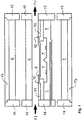
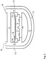
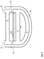
- the reaction chamber has an elongated shape (it is therefore possible to define a longitudinal direction, which in all the figures corresponds to the horizontal direction and even a longitudinal axis given the substantially cylindrical symmetry of the chamber) and comprises four flat walls, which delimit a parallelepiped-shaped reaction and deposition zone; the cross-section of the parallelepiped is a rectangle having a relatively large base and a relatively small height; there is a flat lower wall 1, a flat upper wall 2, a flat left side wall 3 and a flat right side wall 4.
- the chamber comprises other two curved walls 5 and 6; the curved wall 5 is joined by its ends to the ends of the flat wall 1 (e.g.
- the curved wall 6 is joined by its ends to the ends of the flat wall 2 (e.g. see Fig.2 ).
- the walls 1, 2, 3, 4, 5, 6 are shown as if they were made in one piece, but they could be distinct parts, arranged side by side and appropriately joined.
- Such a set of walls is known, for example and in particular, in international patent applications WO 2004/053187 and WO 2004/053188 to which reference is made for further technical details.
- the two arrows drawn in Fig.1 and in Fig.5 represent the incoming flow FI of reaction gases and the outgoing flow FU of exhaust gases; the reaction gases enter the reaction and deposition chamber, chemically react because of the high temperature in this zone, give rise to a deposition of solid material, and exit as exhaust gas (more or less exhausted) from the reaction and deposition zone.
- the heating means of the reaction chamber are not shown in any of the figures; they are typically electromagnetic heating means.
- the reaction chamber comprises a susceptor 7 and a supporting element 8 adapted to support one or more substrates to subject to epitaxial growth simultaneously (each substrate is positioned in a shallow "recess" of the supporting element respectively); the supporting element 8 stably lays on the susceptor 7.
- the susceptor 7 comprises a body (typically cylindrical) underneath and a relief (typically either cylindrical or prismatic) above.
- the supporting element 8 is discoid and is typically circular-shaped; the supporting element 8 is laid stably on the relief of the susceptor 7 and is sized to protrude radially from the relief of the susceptor 7.
- the lower wall 1 has a recess in which the body of the susceptor 7 is placed; typically, recess and body have the same shape; in the example in the figures, recess and body have exactly the same cylindrical shape and nearly the same dimensions (there is only a small difference to allow the rotation of the body in the recess); the body of the susceptor 7 is placed in the recess to be rotational with respect to wall 1; the supporting element 8 rotates as a consequence when the susceptor 7 rotates.
- the reaction chamber comprises a flat covering, corresponding to the components indicated by reference numerals 91 and 92, which are visible in Fig.1 , Fig.3 , Fig.4 and Fig.5 in particular.
- the two components 91 and 92 constitute two conceptually adjacent elements of a single flat covering; such a flat covering extends both longitudinally and transversely for the entire reaction and deposition zone (see Fig.5 in particular), except for the hole 10, as will be described in greater detail below;
- the flat covering could consists of a plurality of adjacent elements; for example, the component 91 and the component 92 could be divided into two, one on a first side, e.g. on the right (considering the longitudinal direction of the chamber) and one on the second side, e.g. on the left of the chamber (considering the longitudinal direction of the chamber).
- such covering elements essentially consist of two flat sheets: a first sheet 91 is located in the inlet zones of the chamber and a second sheet 92 is located in the outlet or exhaust zone of the chamber; reference should be made to arrow FI and to arrow FU for the sake of clarity. It is worth noting that the means used for fixing the covering elements to the chamber, in particular to fix them to the openings of the chamber are not shown in any of the figures.
- flat covering derives from the fact that it is used to cover the wall underneath, which is the lower wall 1, and which is used to make a flat surface (to the greatest possible extent) as lower limit of the reaction and deposition zone - the cross-section of the reaction and deposition zone should be as constant as possible for the entire length of the zone itself to obtain a good growth on the substrates, and rather typically this section is rectangular or at least the lower side is straight.
- the flat covering, whole of the two elements 91 and 92, has a hole 10 at the supporting element 8 (see Fig.1 , Fig.2 and Fig.5 ).
- the shape of the hole 10 corresponds to the shape of the supporting element 8; for the reasons which will be explained below, the shape of the hole 10 is not exactly identical to the shape of the element 8 (in particular, it is slightly greater).
- the upper surfaces of the elements 91 and 92 and the upper surface of the element 8 are aligned ( Fig.1 shows the recess of the element 8 which is exactly filled with a substrate).
- the flat covering has at least one hollow guide (i.e. not in relief) for the passage of a device for loading/unloading the supporting element.
- the covering element 92 has two hollow guides 11 (on the left in Fig.4 ) and 12 (on the right in Fig.4 ) for the passage of a device 16 (see Fig.6 ) for loading/unloading the supporting element 8; both guides 11 and 12 extend starting from the same front edge of the covering element 92 to the hole 10; the hollow guides 11 and 12 are parallel and at the two side edges of the covering element 92; alternatively, such guides may be made, for example, as parallel cuts in the element 92 at a slight distance from the two side edges.
- the cross-section plane in Fig.2 is exactly in the center of the chamber; the cross-section plane in Fig.3 is half way between center and inlet; the cross-section plane in Fig.4 is half way between center and outlet.
- the hole 10 is circle-shaped and the guides 11 and 12 extend to two peripheral zones of the circle opposite with respect to its center (for this reason, the shape of the hole appears as a partial circle).
- the device 16 is used for loading/unloading the supporting element 8 and the chamber is provided with appropriate spaces for passing it and lifting it together with the supporting element.
- the whole of the walls (1, 2, 3, 4, 5 and 6 in the figures) of the chamber which has a substantially cylindrical (or alternatively substantially elliptical) outer shape, is surrounded by heat insulating material, in particular fibrous or porous or foamy graphite; laterally, there is a layer 13 of heat insulating material which is adjacent to the walls 3, 4, 5 and 6; frontally, there is a first layer 14 (in particular, circular or elliptical) made of heat insulating material which is placed at the inlet of the chamber; frontally, there is a second layer 15 (in particular, circular or elliptical) made of heat insulating material which is placed at the outlet of the chamber; the layers 14 and 15 have openings for letting in reaction gases, for letting out exhaust gases and for the other secondary gas flows through the chamber walls.
- heat insulating material in particular fibrous or porous or foamy graphite
- a reaction chamber like the one diagrammatically shown in the figures from Fig.1 to Fig.5 may further have constructive elements, e.g. all or part of those described and illustrated in international patent applications WO 2006/024572 and WO 2007/088420 .
- Fig.6 shows an example of embodiment of a loading/unloading device adapted for the reaction chamber of the figures appended hereto.
- the device 16 is designed to lift and transport the substantially flat discoid element, in particular the supporting element 8; the device 16 can lift and transport elements of various shapes, even if the element 8 is circle-shaped.
- the parts of the device 16 which are used to grip the element 8 correspond substantially to two wings 20 and two shoulders 19; the device 16 is adapted to lift the element 8 by pushing on its lower edge by means of the wings 20. More in detail, the device 16 comprises:
- the shape of the branch of the maneuvering rod could be different from a "V", e.g. it could be semicircle-shaped.
- the length of the rod 18 is such to protrude for a horizontal stretch (e.g. 10-40 cm) from the reaction and deposition zone, in particular from the layer 15, precisely to allow to be maneuvered; typically and advantageously, the rod 18 is adapted to be maneuvered by a robot.
- a horizontal stretch e.g. 10-40 cm
- the device 16 is inserted in the chamber from its outlet, maintaining the chamber horizontal and the device horizontal and orienting the device so that the shoulders 19 and the wings 20 enter the chamber first and then the maneuvering rod 18, which is precisely used to maneuver it.
- the insertion occurs so that the rod 18 and its branch 17 are slightly over the covering 92, the two wings 20 are slightly over the covering 92 and the two shoulders 19 are by the side of the covering 92 of the two guides 11 and 12, respectively.
- the device 16 is made to slide horizontally until the wings 20 reach the side of the element 8 (see Fig.5 ) - the center of the wings 20 is thus substantially in the central cross plane of the chamber where the center of the element 8 is also located.
- the device 16 ( Fig.7C ) is lifted further, the element 8 no longer rests on the susceptor 7 and is sufficiently distanced therefrom, the lower surface of the branch 17 is over the element 8 and slightly distanced therefrom; the wings 20 are in contact with the edge of the element 8.
- the device 16 and the element 8 may be extracted from the chamber by making them slide horizontally backwards towards the outlet of the chamber.
- An element 8 which supports a substrate to be treated is inserted as described above, but in the opposite sense.
- the covering element 92 may be provided with a rod-shaped protrusion (not shown in the figures) adapted to protrude for a horizontal stretch (e.g. 10-40cm) from the reaction and deposition zone, in particular from layer 15.
- the position of the element 92 defines the position of the hole 10 and is closely correlated to the position of the susceptor 7, it is possible to determine when to interrupt the sliding of the device 16 from the outside with good accuracy; in other words, the outer end of the rod-shaped protrusion can be used as horizontal (and vertical) reference for the movements of the device 16.
- the walls of the chamber may be made of graphite, not necessarily coated because of the presence of the covering, i.e. of the elements 91 and 92.
- the susceptor 7 may be made of graphite and does not need to be coated because of the presence of the covering, i.e. of the elements 91 and 92.
- the supporting element 8 may be made of graphite entirely coated with a layer of silicon carbide except for where it supports one or more substrates; the covering is used to avoid, or at least limit, problems of bulging (e.g. related to spurious depositions during the epitaxial growth processes).
- the flat covering in particular the elements 91 and 92, is made of graphite entirely coated with a layer of silicon carbide; the covering is used to avoid or at least limit problems of bulging (e.g. related to spurious depositions during the epitaxial growth processes).
- the loading/unloading device 16 may be made entirely of quartz to be rigid, robust and to prevent problems related to the high temperatures of the chamber. Although the device is made of quartz, it is appropriate to evaluate the loading and unloading temperatures of the element 8 for the device 16 to perform its lifting and transporting functions appropriately.
- the reaction chamber apparatus according to the present invention in particular a reaction chamber as the one described above, is typically used in reactors for epitaxial growth. Being a hot wall chamber with a particular segregation of the reaction and deposition zone with a particular solution for transferring energy to the chamber for heating it, it is particular adapted for the reactors which require very high temperatures, e.g.
Landscapes
- Chemical & Material Sciences (AREA)
- Engineering & Computer Science (AREA)
- Materials Engineering (AREA)
- Metallurgy (AREA)
- Organic Chemistry (AREA)
- Chemical Kinetics & Catalysis (AREA)
- General Chemical & Material Sciences (AREA)
- Crystallography & Structural Chemistry (AREA)
- Mechanical Engineering (AREA)
- Inorganic Chemistry (AREA)
- Crystals, And After-Treatments Of Crystals (AREA)
- Chemical Vapour Deposition (AREA)
- Robotics (AREA)
- Container, Conveyance, Adherence, Positioning, Of Wafer (AREA)
Claims (10)
- Reaktionskammer eines Reaktors für Epitaxialwachstum, umfassend:- eine Wand (1) mit einer Aussparung,- einen Suszeptor (7), umfassend einen Körper und ein Relief, wobei der Körper in der Aussparung platziert ist, um so bezüglich der Wand (1) drehfähig zu sein,- ein scheibenförmiges Trägerelement (8), angepasst, um stabil auf dem Relief gelegt zu werden, das eine Gestalt mit einer solchen Größe aufweist, um radial von dem Relief hervorzustehen und angepasst ist, um ein oder mehrere Substrate zu tragen, die epitaxialem Wachstum zu unterziehen sind, und- eine ebene Abdeckung (91, 92), die sich über der Wand (1) befindet und ein Loch (10) bei dem scheibenförmigen Trägerelement (8) aufweist;wobei die Gestalt des Lochs (10) der Gestalt des scheibenförmigen Trägerelements (8) entspricht;
wobei die Abdeckung (92) mindestens eine hohle Führung (11, 12) für den Durchgang einer Vorrichtung (16) zum Beladen/Entladen des scheibenförmigen Trägerelements (8) aufweist, wobei die hohle Führung (11, 12) sich ausgehend von einer Kante der Abdeckung (92) zu dem Loch (10) erstreckt. - Reaktionskammer nach Anspruch 1, wobei die Abdeckung (92) eine erste hohle Führung (11) und eine zweite hohle Führung (12) aufweist, wobei die erste und zweite hohle Führung (11, 12) sich ausgehend von einer Kante der Abdeckung (92) zu dem Loch (10) erstrecken.
- Reaktionskammer nach Anspruch 2, wobei die erste und zweite hohle Führung (11, 12) parallel sind.
- Reaktionskammer nach Anspruch 3, wobei die erste und zweite hohle Führung (11, 12) sich bei den zwei Seitenkanten der Abdeckung (92) befinden.
- Reaktionskammer nach Anspruch 2 oder 3 oder 4, wobei das Loch (10) kreisförmig ist, und wobei die erste und zweite hohle Führung (11, 12) sich zu zwei peripheren Zonen des Kreises, bezüglich seiner Mitte entgegengesetzt, erstrecken.
- Reaktionskammer nach einem der vorstehenden Ansprüche,
wobei die Wand (1) aus unbeschichtetem Grafit hergestellt ist;
wobei der Suszeptor (7) aus unbeschichtetem Grafit hergestellt ist;
wobei das Trägerelement (8) aus vollständig mit einer Schicht aus Siliziumcarbid beschichtetem Grafit hergestellt ist, ausgenommen dort, wo es ein oder mehrere Substrate trägt;
wobei die ebene Abdeckung (91, 92) aus vollständig mit einer Schicht aus Siliziumcarbid beschichtetem Grafit hergestellt ist. - Reaktionskammer nach einem der vorstehenden Ansprüche, versehen mit einer Vorrichtung (16) zum Beladen/Entladen des Trägerelements (8), das zum Anheben des Trägerelements (8) durch Drücken auf die Kante von der Unterseite davon angepasst ist.
- Reaktionskammer nach Anspruch 7, wobei die Vorrichtung (16) zum Beladen/Entladen umfasst:- mindestens einen Manövrierstab (18),- zwei Schultern (19), verbunden (17) mit dem mindestens einen Manövrierstab (18) und angepasst zum Gleiten in den hohlen Führungen (11, 12), und- zwei Flügel (20), jeweils mit den zwei Schultern (19) verbunden und angepasst, um von der Unterseite auf die Kante des Trägerelements (8) zu drücken.
- Reaktionskammer nach Anspruch 7 oder 8, wobei die Vorrichtung (16) zum Beladen/Entladen vollständig aus Quarz hergestellt ist.
- Reaktor zum Epitaxialwachstum, umfassend eine Reaktionskammer nach einem der vorstehenden Ansprüche.
Applications Claiming Priority (2)
| Application Number | Priority Date | Filing Date | Title |
|---|---|---|---|
| IT000073A ITCO20130073A1 (it) | 2013-12-19 | 2013-12-19 | Camera di reazione di un reattore per crescite epitassiali adatta per l'uso con un dispositivo di carico/scarico e reattore |
| PCT/IB2014/002801 WO2015092525A1 (en) | 2013-12-19 | 2014-12-17 | Reaction chamber for epitaxial growth with a loading/unloading device and reactor |
Publications (2)
| Publication Number | Publication Date |
|---|---|
| EP3084034A1 EP3084034A1 (de) | 2016-10-26 |
| EP3084034B1 true EP3084034B1 (de) | 2018-02-21 |
Family
ID=50190540
Family Applications (1)
| Application Number | Title | Priority Date | Filing Date |
|---|---|---|---|
| EP14833165.5A Active EP3084034B1 (de) | 2013-12-19 | 2014-12-17 | Reaktionskammer zum epitaktischen wachstum mit einer lade-/entladevorrichtung und reaktor |
Country Status (6)
| Country | Link |
|---|---|
| US (1) | US10392723B2 (de) |
| EP (1) | EP3084034B1 (de) |
| JP (1) | JP6505105B2 (de) |
| CN (1) | CN105849311B (de) |
| IT (1) | ITCO20130073A1 (de) |
| WO (1) | WO2015092525A1 (de) |
Families Citing this family (10)
| Publication number | Priority date | Publication date | Assignee | Title |
|---|---|---|---|---|
| DE102015223807A1 (de) * | 2015-12-01 | 2017-06-01 | Siltronic Ag | Verfahren zur Herstellung einer Halbleiterscheibe mit epitaktischer Schicht in einer Abscheidekammer, Vorrichtung zur Herstellung einer Halbleiterscheibe mit epitaktischer Schicht und Halbleiterscheibe mit epitaktischer Schicht |
| IT201800011158A1 (it) * | 2018-12-17 | 2020-06-17 | Lpe Spa | Camera di reazione per un reattore epitassiale di materiale semiconduttore con sezione longitudinale non-uniforme e reattore |
| JP7670696B2 (ja) | 2019-10-03 | 2025-04-30 | エルピーイー ソシエタ ペル アチオニ | ローディング又はアンローディング群およびエピタキシャル反応器を有する処理装置 |
| US12522949B2 (en) | 2019-10-03 | 2026-01-13 | Lpe S.P.A. | Treating arrangement with storage chamber and epitaxial reactor |
| JP7564870B2 (ja) | 2019-10-03 | 2024-10-09 | エルピーイー ソシエタ ペル アチオニ | 搬送チャンバおよびエピタキシャル反応器を有する処理装置 |
| IT201900022047A1 (it) | 2019-11-25 | 2021-05-25 | Lpe Spa | Dispositivo di supporto substrati per una camera di reazione di un reattore epitassiale con rotazione a flusso di gas, camera di reazione e reattore epitassiale |
| IT202000021517A1 (it) | 2020-09-11 | 2022-03-11 | Lpe Spa | Metodo per deposizione cvd di carburo di silicio con drogaggio di tipo n e reattore epitassiale |
| IT202300018780A1 (it) | 2023-09-13 | 2025-03-13 | Lpe Spa | Reattore per deposizione epitassiale di materiale semiconduttore su substrati con slitta scorrevole per camera di reazione |
| JP2026028237A (ja) | 2024-08-06 | 2026-02-19 | エルピーイー・エッセ・ピ・ア | 反応器部品からの炭化ケイ素膜のエッチング |
| JP2026053295A (ja) | 2024-09-12 | 2026-03-25 | エルピーイー・エッセ・ピ・ア | 反応チャンバ部品からの炭化ケイ素膜の光子アシスト化学エッチング |
Family Cites Families (19)
| Publication number | Priority date | Publication date | Assignee | Title |
|---|---|---|---|---|
| KR0148714B1 (ko) * | 1995-08-01 | 1998-08-17 | 황철주 | 매엽식 저압화학증기증착기의 서셉터 장치 |
| US6133152A (en) * | 1997-05-16 | 2000-10-17 | Applied Materials, Inc. | Co-rotating edge ring extension for use in a semiconductor processing chamber |
| US6530994B1 (en) * | 1997-08-15 | 2003-03-11 | Micro C Technologies, Inc. | Platform for supporting a semiconductor substrate and method of supporting a substrate during rapid high temperature processing |
| US6096135A (en) * | 1998-07-21 | 2000-08-01 | Applied Materials, Inc. | Method and apparatus for reducing contamination of a substrate in a substrate processing system |
| US6537011B1 (en) * | 2000-03-10 | 2003-03-25 | Applied Materials, Inc. | Method and apparatus for transferring and supporting a substrate |
| US20030114016A1 (en) * | 2001-12-18 | 2003-06-19 | Tischler Michael A. | Wafer carrier for semiconductor process tool |
| DE10232731A1 (de) * | 2002-07-19 | 2004-02-05 | Aixtron Ag | Be- und Entladevorrichtung für eine Beschichtungseinrichtung |
| ATE423226T1 (de) | 2002-12-10 | 2009-03-15 | E T C Epitaxial Technology Ct | Suszeptorsystem |
| WO2004053187A1 (en) | 2002-12-10 | 2004-06-24 | E.T.C. Epitaxial Technology Center Srl | Susceptor system________________________ |
| JP2004327761A (ja) * | 2003-04-25 | 2004-11-18 | Sumitomo Mitsubishi Silicon Corp | エピタキシャル成長用サセプタ |
| US7771538B2 (en) * | 2004-01-20 | 2010-08-10 | Jusung Engineering Co., Ltd. | Substrate supporting means having wire and apparatus using the same |
| WO2005121417A1 (en) | 2004-06-09 | 2005-12-22 | E.T.C. Epitaxial Technology Center S.R.L. | Support system for treatment apparatuses |
| ITMI20041677A1 (it) | 2004-08-30 | 2004-11-30 | E T C Epitaxial Technology Ct | Processo di pulitura e processo operativo per un reattore cvd. |
| WO2006038228A1 (en) * | 2004-10-01 | 2006-04-13 | Lpe Spa | Epitaxial reactor cooling method and reactor cooled thereby |
| ITMI20050645A1 (it) * | 2005-04-14 | 2006-10-15 | Lpe Spa | Suscettori per reattori epitassiali e utensile per maneggiarlo |
| US20080210169A1 (en) * | 2005-07-21 | 2008-09-04 | Lpe S.P.A. | System for Supporting and Rotating a Susceptor Inside a Treatment Chamber of a Wafer Treating Apparatus |
| ITMI20052498A1 (it) | 2005-12-28 | 2007-06-29 | Lpe Spa | Camera di reazione a temperatura differenziata |
| DE102010017082A1 (de) * | 2010-05-26 | 2011-12-01 | Aixtron Ag | Vorrichtung und Verfahren zum Be- und Entladen, insbesondere einer Beschichtungseinrichtung |
| KR101928356B1 (ko) * | 2012-02-16 | 2018-12-12 | 엘지이노텍 주식회사 | 반도체 제조 장치 |
-
2013
- 2013-12-19 IT IT000073A patent/ITCO20130073A1/it unknown
-
2014
- 2014-12-17 JP JP2016539076A patent/JP6505105B2/ja active Active
- 2014-12-17 US US15/104,482 patent/US10392723B2/en active Active
- 2014-12-17 EP EP14833165.5A patent/EP3084034B1/de active Active
- 2014-12-17 CN CN201480067668.6A patent/CN105849311B/zh active Active
- 2014-12-17 WO PCT/IB2014/002801 patent/WO2015092525A1/en not_active Ceased
Also Published As
| Publication number | Publication date |
|---|---|
| US10392723B2 (en) | 2019-08-27 |
| EP3084034A1 (de) | 2016-10-26 |
| ITCO20130073A1 (it) | 2015-06-20 |
| WO2015092525A1 (en) | 2015-06-25 |
| CN105849311A (zh) | 2016-08-10 |
| CN105849311B (zh) | 2018-11-13 |
| US20160312382A1 (en) | 2016-10-27 |
| JP6505105B2 (ja) | 2019-04-24 |
| JP2017503342A (ja) | 2017-01-26 |
Similar Documents
| Publication | Publication Date | Title |
|---|---|---|
| US10392723B2 (en) | Reaction chamber for epitaxial growth with a loading/unloading device and reactor | |
| US20090004405A1 (en) | Thermal Batch Reactor with Removable Susceptors | |
| KR102649605B1 (ko) | 프로세싱 챔버를 위한 고온 가열기 | |
| US20100107974A1 (en) | Substrate holder with varying density | |
| US20180138031A1 (en) | Process chamber having separate process gas and purge gas regions | |
| KR102459367B1 (ko) | 에피 챔버를 위한 라이너 | |
| KR20180082574A (ko) | 웨이퍼 지지 기구, 화학 기상 성장 장치 및 에피택셜 웨이퍼의 제조 방법 | |
| KR20180085822A (ko) | 기판에 걸친 온도 프로파일을 최소화하기 위한 홈들을 갖는 평판형 서셉터 | |
| JP2012517526A (ja) | 化学気相成長システムおよび化学気相成長プロセス | |
| US20200181798A1 (en) | Susceptor and chemical vapor deposition apparatus | |
| KR101625478B1 (ko) | 수직 적층식 히터를 구비한 박막 증착 장치 및 이를 이용한 박막 증착 방법 | |
| KR20150037561A (ko) | 열처리 장치 및 열처리 방법 | |
| KR101152598B1 (ko) | 기판처리장치 | |
| KR20210072116A (ko) | 성막 방법, 성막 장치, 서셉터 유닛, 및 서셉터 유닛에 사용되는 스페이서 세트 | |
| US20160068958A1 (en) | Lamp Heater For Atomic Layer Deposition | |
| JP6341561B2 (ja) | 気相成長装置 | |
| KR101361711B1 (ko) | 공정챔버의 지지유닛 및 이를 포함하는 기판처리장치 | |
| KR101651882B1 (ko) | 기판처리장치 | |
| KR101497373B1 (ko) | 반응가스의 혼합 및 가열수단을 구비한 서셉터 제조장치 | |
| KR102711633B1 (ko) | 퇴적 반응기의 챔버 내에서 에피택셜층을 가진 반도체 웨이퍼를 생산하기 위한 방법 | |
| EP3263748A2 (de) | Cvd-reaktor mit beheizter mehrzonen-prozesskammer | |
| CN205845916U (zh) | 用于处理基板的设备 | |
| KR101500938B1 (ko) | 반응가스의 혼합 및 가열수단을 구비한 서셉터 제조장치 | |
| KR20240169536A (ko) | 웨이퍼 핸들링 어셈블리 | |
| KR20240019036A (ko) | 웨이퍼 보트 및 복수의 기판 상에 층을 형성하기 위한 방법 |
Legal Events
| Date | Code | Title | Description |
|---|---|---|---|
| PUAI | Public reference made under article 153(3) epc to a published international application that has entered the european phase |
Free format text: ORIGINAL CODE: 0009012 |
|
| 17P | Request for examination filed |
Effective date: 20160629 |
|
| AK | Designated contracting states |
Kind code of ref document: A1 Designated state(s): AL AT BE BG CH CY CZ DE DK EE ES FI FR GB GR HR HU IE IS IT LI LT LU LV MC MK MT NL NO PL PT RO RS SE SI SK SM TR |
|
| AX | Request for extension of the european patent |
Extension state: BA ME |
|
| RIN1 | Information on inventor provided before grant (corrected) |
Inventor name: COREA, FRANCESCO Inventor name: GOBBO, LAURA Inventor name: CRIPPA, DANILO Inventor name: OGLIARI, VINCENZO Inventor name: PRETI, FRANCO Inventor name: VECCHIO, CARMELO Inventor name: PUGLISI, MARCO Inventor name: MAUCERI, MARCO |
|
| DAX | Request for extension of the european patent (deleted) | ||
| STAA | Information on the status of an ep patent application or granted ep patent |
Free format text: STATUS: EXAMINATION IS IN PROGRESS |
|
| 17Q | First examination report despatched |
Effective date: 20170518 |
|
| GRAP | Despatch of communication of intention to grant a patent |
Free format text: ORIGINAL CODE: EPIDOSNIGR1 |
|
| STAA | Information on the status of an ep patent application or granted ep patent |
Free format text: STATUS: GRANT OF PATENT IS INTENDED |
|
| INTG | Intention to grant announced |
Effective date: 20170714 |
|
| RIN1 | Information on inventor provided before grant (corrected) |
Inventor name: PRETI, FRANCO Inventor name: GOBBO, LAURA Inventor name: VECCHIO, CARMELO Inventor name: MAUCERI, MARCO Inventor name: PUGLISI, MARCO Inventor name: CRIPPA, DANILO Inventor name: COREA, FRANCESCO Inventor name: OGLIARI, VINCENZO |
|
| GRAS | Grant fee paid |
Free format text: ORIGINAL CODE: EPIDOSNIGR3 |
|
| GRAA | (expected) grant |
Free format text: ORIGINAL CODE: 0009210 |
|
| STAA | Information on the status of an ep patent application or granted ep patent |
Free format text: STATUS: THE PATENT HAS BEEN GRANTED |
|
| AK | Designated contracting states |
Kind code of ref document: B1 Designated state(s): AL AT BE BG CH CY CZ DE DK EE ES FI FR GB GR HR HU IE IS IT LI LT LU LV MC MK MT NL NO PL PT RO RS SE SI SK SM TR |
|
| REG | Reference to a national code |
Ref country code: GB Ref legal event code: FG4D |
|
| REG | Reference to a national code |
Ref country code: CH Ref legal event code: EP |
|
| REG | Reference to a national code |
Ref country code: AT Ref legal event code: REF Ref document number: 971811 Country of ref document: AT Kind code of ref document: T Effective date: 20180315 |
|
| REG | Reference to a national code |
Ref country code: IE Ref legal event code: FG4D |
|
| REG | Reference to a national code |
Ref country code: DE Ref legal event code: R096 Ref document number: 602014021443 Country of ref document: DE |
|
| REG | Reference to a national code |
Ref country code: SE Ref legal event code: TRGR |
|
| REG | Reference to a national code |
Ref country code: NL Ref legal event code: MP Effective date: 20180221 |
|
| REG | Reference to a national code |
Ref country code: LT Ref legal event code: MG4D |
|
| REG | Reference to a national code |
Ref country code: AT Ref legal event code: MK05 Ref document number: 971811 Country of ref document: AT Kind code of ref document: T Effective date: 20180221 |
|
| PG25 | Lapsed in a contracting state [announced via postgrant information from national office to epo] |
Ref country code: NO Free format text: LAPSE BECAUSE OF FAILURE TO SUBMIT A TRANSLATION OF THE DESCRIPTION OR TO PAY THE FEE WITHIN THE PRESCRIBED TIME-LIMIT Effective date: 20180521 Ref country code: CY Free format text: LAPSE BECAUSE OF FAILURE TO SUBMIT A TRANSLATION OF THE DESCRIPTION OR TO PAY THE FEE WITHIN THE PRESCRIBED TIME-LIMIT Effective date: 20180221 Ref country code: HR Free format text: LAPSE BECAUSE OF FAILURE TO SUBMIT A TRANSLATION OF THE DESCRIPTION OR TO PAY THE FEE WITHIN THE PRESCRIBED TIME-LIMIT Effective date: 20180221 Ref country code: NL Free format text: LAPSE BECAUSE OF FAILURE TO SUBMIT A TRANSLATION OF THE DESCRIPTION OR TO PAY THE FEE WITHIN THE PRESCRIBED TIME-LIMIT Effective date: 20180221 Ref country code: LT Free format text: LAPSE BECAUSE OF FAILURE TO SUBMIT A TRANSLATION OF THE DESCRIPTION OR TO PAY THE FEE WITHIN THE PRESCRIBED TIME-LIMIT Effective date: 20180221 Ref country code: ES Free format text: LAPSE BECAUSE OF FAILURE TO SUBMIT A TRANSLATION OF THE DESCRIPTION OR TO PAY THE FEE WITHIN THE PRESCRIBED TIME-LIMIT Effective date: 20180221 Ref country code: FI Free format text: LAPSE BECAUSE OF FAILURE TO SUBMIT A TRANSLATION OF THE DESCRIPTION OR TO PAY THE FEE WITHIN THE PRESCRIBED TIME-LIMIT Effective date: 20180221 |
|
| PG25 | Lapsed in a contracting state [announced via postgrant information from national office to epo] |
Ref country code: AT Free format text: LAPSE BECAUSE OF FAILURE TO SUBMIT A TRANSLATION OF THE DESCRIPTION OR TO PAY THE FEE WITHIN THE PRESCRIBED TIME-LIMIT Effective date: 20180221 Ref country code: GR Free format text: LAPSE BECAUSE OF FAILURE TO SUBMIT A TRANSLATION OF THE DESCRIPTION OR TO PAY THE FEE WITHIN THE PRESCRIBED TIME-LIMIT Effective date: 20180522 Ref country code: BG Free format text: LAPSE BECAUSE OF FAILURE TO SUBMIT A TRANSLATION OF THE DESCRIPTION OR TO PAY THE FEE WITHIN THE PRESCRIBED TIME-LIMIT Effective date: 20180521 Ref country code: LV Free format text: LAPSE BECAUSE OF FAILURE TO SUBMIT A TRANSLATION OF THE DESCRIPTION OR TO PAY THE FEE WITHIN THE PRESCRIBED TIME-LIMIT Effective date: 20180221 Ref country code: RS Free format text: LAPSE BECAUSE OF FAILURE TO SUBMIT A TRANSLATION OF THE DESCRIPTION OR TO PAY THE FEE WITHIN THE PRESCRIBED TIME-LIMIT Effective date: 20180221 |
|
| PG25 | Lapsed in a contracting state [announced via postgrant information from national office to epo] |
Ref country code: PL Free format text: LAPSE BECAUSE OF FAILURE TO SUBMIT A TRANSLATION OF THE DESCRIPTION OR TO PAY THE FEE WITHIN THE PRESCRIBED TIME-LIMIT Effective date: 20180221 Ref country code: AL Free format text: LAPSE BECAUSE OF FAILURE TO SUBMIT A TRANSLATION OF THE DESCRIPTION OR TO PAY THE FEE WITHIN THE PRESCRIBED TIME-LIMIT Effective date: 20180221 Ref country code: RO Free format text: LAPSE BECAUSE OF FAILURE TO SUBMIT A TRANSLATION OF THE DESCRIPTION OR TO PAY THE FEE WITHIN THE PRESCRIBED TIME-LIMIT Effective date: 20180221 Ref country code: EE Free format text: LAPSE BECAUSE OF FAILURE TO SUBMIT A TRANSLATION OF THE DESCRIPTION OR TO PAY THE FEE WITHIN THE PRESCRIBED TIME-LIMIT Effective date: 20180221 |
|
| REG | Reference to a national code |
Ref country code: DE Ref legal event code: R097 Ref document number: 602014021443 Country of ref document: DE |
|
| PG25 | Lapsed in a contracting state [announced via postgrant information from national office to epo] |
Ref country code: CZ Free format text: LAPSE BECAUSE OF FAILURE TO SUBMIT A TRANSLATION OF THE DESCRIPTION OR TO PAY THE FEE WITHIN THE PRESCRIBED TIME-LIMIT Effective date: 20180221 Ref country code: SM Free format text: LAPSE BECAUSE OF FAILURE TO SUBMIT A TRANSLATION OF THE DESCRIPTION OR TO PAY THE FEE WITHIN THE PRESCRIBED TIME-LIMIT Effective date: 20180221 Ref country code: DK Free format text: LAPSE BECAUSE OF FAILURE TO SUBMIT A TRANSLATION OF THE DESCRIPTION OR TO PAY THE FEE WITHIN THE PRESCRIBED TIME-LIMIT Effective date: 20180221 Ref country code: SK Free format text: LAPSE BECAUSE OF FAILURE TO SUBMIT A TRANSLATION OF THE DESCRIPTION OR TO PAY THE FEE WITHIN THE PRESCRIBED TIME-LIMIT Effective date: 20180221 |
|
| PLBE | No opposition filed within time limit |
Free format text: ORIGINAL CODE: 0009261 |
|
| STAA | Information on the status of an ep patent application or granted ep patent |
Free format text: STATUS: NO OPPOSITION FILED WITHIN TIME LIMIT |
|
| 26N | No opposition filed |
Effective date: 20181122 |
|
| PG25 | Lapsed in a contracting state [announced via postgrant information from national office to epo] |
Ref country code: SI Free format text: LAPSE BECAUSE OF FAILURE TO SUBMIT A TRANSLATION OF THE DESCRIPTION OR TO PAY THE FEE WITHIN THE PRESCRIBED TIME-LIMIT Effective date: 20180221 |
|
| REG | Reference to a national code |
Ref country code: CH Ref legal event code: PL |
|
| PG25 | Lapsed in a contracting state [announced via postgrant information from national office to epo] |
Ref country code: MC Free format text: LAPSE BECAUSE OF FAILURE TO SUBMIT A TRANSLATION OF THE DESCRIPTION OR TO PAY THE FEE WITHIN THE PRESCRIBED TIME-LIMIT Effective date: 20180221 Ref country code: LU Free format text: LAPSE BECAUSE OF NON-PAYMENT OF DUE FEES Effective date: 20181217 |
|
| REG | Reference to a national code |
Ref country code: IE Ref legal event code: MM4A |
|
| REG | Reference to a national code |
Ref country code: BE Ref legal event code: MM Effective date: 20181231 |
|
| PG25 | Lapsed in a contracting state [announced via postgrant information from national office to epo] |
Ref country code: IE Free format text: LAPSE BECAUSE OF NON-PAYMENT OF DUE FEES Effective date: 20181217 |
|
| PG25 | Lapsed in a contracting state [announced via postgrant information from national office to epo] |
Ref country code: BE Free format text: LAPSE BECAUSE OF NON-PAYMENT OF DUE FEES Effective date: 20181231 |
|
| PG25 | Lapsed in a contracting state [announced via postgrant information from national office to epo] |
Ref country code: CH Free format text: LAPSE BECAUSE OF NON-PAYMENT OF DUE FEES Effective date: 20181231 Ref country code: LI Free format text: LAPSE BECAUSE OF NON-PAYMENT OF DUE FEES Effective date: 20181231 |
|
| PG25 | Lapsed in a contracting state [announced via postgrant information from national office to epo] |
Ref country code: MT Free format text: LAPSE BECAUSE OF NON-PAYMENT OF DUE FEES Effective date: 20181217 |
|
| PG25 | Lapsed in a contracting state [announced via postgrant information from national office to epo] |
Ref country code: TR Free format text: LAPSE BECAUSE OF FAILURE TO SUBMIT A TRANSLATION OF THE DESCRIPTION OR TO PAY THE FEE WITHIN THE PRESCRIBED TIME-LIMIT Effective date: 20180221 |
|
| PG25 | Lapsed in a contracting state [announced via postgrant information from national office to epo] |
Ref country code: PT Free format text: LAPSE BECAUSE OF FAILURE TO SUBMIT A TRANSLATION OF THE DESCRIPTION OR TO PAY THE FEE WITHIN THE PRESCRIBED TIME-LIMIT Effective date: 20180221 |
|
| PG25 | Lapsed in a contracting state [announced via postgrant information from national office to epo] |
Ref country code: HU Free format text: LAPSE BECAUSE OF FAILURE TO SUBMIT A TRANSLATION OF THE DESCRIPTION OR TO PAY THE FEE WITHIN THE PRESCRIBED TIME-LIMIT; INVALID AB INITIO Effective date: 20141217 Ref country code: MK Free format text: LAPSE BECAUSE OF NON-PAYMENT OF DUE FEES Effective date: 20180221 |
|
| PG25 | Lapsed in a contracting state [announced via postgrant information from national office to epo] |
Ref country code: IS Free format text: LAPSE BECAUSE OF FAILURE TO SUBMIT A TRANSLATION OF THE DESCRIPTION OR TO PAY THE FEE WITHIN THE PRESCRIBED TIME-LIMIT Effective date: 20180621 |
|
| PGFP | Annual fee paid to national office [announced via postgrant information from national office to epo] |
Ref country code: GB Payment date: 20251229 Year of fee payment: 12 |
|
| PGFP | Annual fee paid to national office [announced via postgrant information from national office to epo] |
Ref country code: IT Payment date: 20251219 Year of fee payment: 12 |
|
| PGFP | Annual fee paid to national office [announced via postgrant information from national office to epo] |
Ref country code: FR Payment date: 20251226 Year of fee payment: 12 |
|
| PGFP | Annual fee paid to national office [announced via postgrant information from national office to epo] |
Ref country code: SE Payment date: 20251227 Year of fee payment: 12 |
|
| PGFP | Annual fee paid to national office [announced via postgrant information from national office to epo] |
Ref country code: DE Payment date: 20251229 Year of fee payment: 12 |