EP3055882B1 - Mehrschichtiges substrat für eine halbleiterverkapselung und verfahrren - Google Patents
Mehrschichtiges substrat für eine halbleiterverkapselung und verfahrren Download PDFInfo
- Publication number
- EP3055882B1 EP3055882B1 EP14891614.1A EP14891614A EP3055882B1 EP 3055882 B1 EP3055882 B1 EP 3055882B1 EP 14891614 A EP14891614 A EP 14891614A EP 3055882 B1 EP3055882 B1 EP 3055882B1
- Authority
- EP
- European Patent Office
- Prior art keywords
- layer
- distance
- substrate
- thickness
- individual locations
- Prior art date
- Legal status (The legal status is an assumption and is not a legal conclusion. Google has not performed a legal analysis and makes no representation as to the accuracy of the status listed.)
- Active
Links
Images



Classifications
-
- H—ELECTRICITY
- H05—ELECTRIC TECHNIQUES NOT OTHERWISE PROVIDED FOR
- H05K—PRINTED CIRCUITS; CASINGS OR CONSTRUCTIONAL DETAILS OF ELECTRIC APPARATUS; MANUFACTURE OF ASSEMBLAGES OF ELECTRICAL COMPONENTS
- H05K1/00—Printed circuits
- H05K1/02—Details
- H05K1/0271—Arrangements for reducing stress or warp in rigid printed circuit boards, e.g. caused by loads, vibrations or differences in thermal expansion
-
- H—ELECTRICITY
- H05—ELECTRIC TECHNIQUES NOT OTHERWISE PROVIDED FOR
- H05K—PRINTED CIRCUITS; CASINGS OR CONSTRUCTIONAL DETAILS OF ELECTRIC APPARATUS; MANUFACTURE OF ASSEMBLAGES OF ELECTRICAL COMPONENTS
- H05K1/00—Printed circuits
- H05K1/02—Details
- H05K1/03—Use of materials for the substrate
- H05K1/0313—Organic insulating material
- H05K1/0353—Organic insulating material consisting of two or more materials, e.g. two or more polymers, polymer + filler, + reinforcement
- H05K1/036—Multilayers with layers of different types
-
- H—ELECTRICITY
- H05—ELECTRIC TECHNIQUES NOT OTHERWISE PROVIDED FOR
- H05K—PRINTED CIRCUITS; CASINGS OR CONSTRUCTIONAL DETAILS OF ELECTRIC APPARATUS; MANUFACTURE OF ASSEMBLAGES OF ELECTRICAL COMPONENTS
- H05K3/00—Apparatus or processes for manufacturing printed circuits
- H05K3/0011—Working of insulating substrates or insulating layers
- H05K3/0014—Shaping of the substrate, e.g. by moulding
-
- H—ELECTRICITY
- H10—SEMICONDUCTOR DEVICES; ELECTRIC SOLID-STATE DEVICES NOT OTHERWISE PROVIDED FOR
- H10P—GENERIC PROCESSES OR APPARATUS FOR THE MANUFACTURE OR TREATMENT OF DEVICES COVERED BY CLASS H10
- H10P72/00—Handling or holding of wafers, substrates or devices during manufacture or treatment thereof
- H10P72/70—Handling or holding of wafers, substrates or devices during manufacture or treatment thereof for supporting or gripping
- H10P72/74—Handling or holding of wafers, substrates or devices during manufacture or treatment thereof for supporting or gripping using temporarily an auxiliary support
-
- H—ELECTRICITY
- H10—SEMICONDUCTOR DEVICES; ELECTRIC SOLID-STATE DEVICES NOT OTHERWISE PROVIDED FOR
- H10P—GENERIC PROCESSES OR APPARATUS FOR THE MANUFACTURE OR TREATMENT OF DEVICES COVERED BY CLASS H10
- H10P90/00—Preparation of wafers not covered by a single main group of this subclass, e.g. wafer reinforcement
-
- H—ELECTRICITY
- H10—SEMICONDUCTOR DEVICES; ELECTRIC SOLID-STATE DEVICES NOT OTHERWISE PROVIDED FOR
- H10P—GENERIC PROCESSES OR APPARATUS FOR THE MANUFACTURE OR TREATMENT OF DEVICES COVERED BY CLASS H10
- H10P90/00—Preparation of wafers not covered by a single main group of this subclass, e.g. wafer reinforcement
- H10P90/12—Preparing bulk and homogeneous wafers
-
- H—ELECTRICITY
- H10—SEMICONDUCTOR DEVICES; ELECTRIC SOLID-STATE DEVICES NOT OTHERWISE PROVIDED FOR
- H10P—GENERIC PROCESSES OR APPARATUS FOR THE MANUFACTURE OR TREATMENT OF DEVICES COVERED BY CLASS H10
- H10P90/00—Preparation of wafers not covered by a single main group of this subclass, e.g. wafer reinforcement
- H10P90/12—Preparing bulk and homogeneous wafers
- H10P90/18—Preparing bulk and homogeneous wafers by shaping
-
- H—ELECTRICITY
- H10—SEMICONDUCTOR DEVICES; ELECTRIC SOLID-STATE DEVICES NOT OTHERWISE PROVIDED FOR
- H10W—GENERIC PACKAGES, INTERCONNECTIONS, CONNECTORS OR OTHER CONSTRUCTIONAL DETAILS OF DEVICES COVERED BY CLASS H10
- H10W70/00—Package substrates; Interposers; Redistribution layers [RDL]
- H10W70/01—Manufacture or treatment
- H10W70/05—Manufacture or treatment of insulating or insulated package substrates, or of interposers, or of redistribution layers
-
- H—ELECTRICITY
- H10—SEMICONDUCTOR DEVICES; ELECTRIC SOLID-STATE DEVICES NOT OTHERWISE PROVIDED FOR
- H10W—GENERIC PACKAGES, INTERCONNECTIONS, CONNECTORS OR OTHER CONSTRUCTIONAL DETAILS OF DEVICES COVERED BY CLASS H10
- H10W70/00—Package substrates; Interposers; Redistribution layers [RDL]
- H10W70/60—Insulating or insulated package substrates; Interposers; Redistribution layers
-
- H—ELECTRICITY
- H10—SEMICONDUCTOR DEVICES; ELECTRIC SOLID-STATE DEVICES NOT OTHERWISE PROVIDED FOR
- H10W—GENERIC PACKAGES, INTERCONNECTIONS, CONNECTORS OR OTHER CONSTRUCTIONAL DETAILS OF DEVICES COVERED BY CLASS H10
- H10W70/00—Package substrates; Interposers; Redistribution layers [RDL]
- H10W70/60—Insulating or insulated package substrates; Interposers; Redistribution layers
- H10W70/62—Insulating or insulated package substrates; Interposers; Redistribution layers characterised by their interconnections
- H10W70/65—Shapes or dispositions of interconnections
-
- H—ELECTRICITY
- H10—SEMICONDUCTOR DEVICES; ELECTRIC SOLID-STATE DEVICES NOT OTHERWISE PROVIDED FOR
- H10W—GENERIC PACKAGES, INTERCONNECTIONS, CONNECTORS OR OTHER CONSTRUCTIONAL DETAILS OF DEVICES COVERED BY CLASS H10
- H10W70/00—Package substrates; Interposers; Redistribution layers [RDL]
- H10W70/60—Insulating or insulated package substrates; Interposers; Redistribution layers
- H10W70/67—Insulating or insulated package substrates; Interposers; Redistribution layers characterised by their insulating layers or insulating parts
- H10W70/68—Shapes or dispositions thereof
-
- H—ELECTRICITY
- H10—SEMICONDUCTOR DEVICES; ELECTRIC SOLID-STATE DEVICES NOT OTHERWISE PROVIDED FOR
- H10W—GENERIC PACKAGES, INTERCONNECTIONS, CONNECTORS OR OTHER CONSTRUCTIONAL DETAILS OF DEVICES COVERED BY CLASS H10
- H10W70/00—Package substrates; Interposers; Redistribution layers [RDL]
- H10W70/60—Insulating or insulated package substrates; Interposers; Redistribution layers
- H10W70/67—Insulating or insulated package substrates; Interposers; Redistribution layers characterised by their insulating layers or insulating parts
- H10W70/68—Shapes or dispositions thereof
- H10W70/685—Shapes or dispositions thereof comprising multiple insulating layers
-
- H—ELECTRICITY
- H10—SEMICONDUCTOR DEVICES; ELECTRIC SOLID-STATE DEVICES NOT OTHERWISE PROVIDED FOR
- H10W—GENERIC PACKAGES, INTERCONNECTIONS, CONNECTORS OR OTHER CONSTRUCTIONAL DETAILS OF DEVICES COVERED BY CLASS H10
- H10W70/00—Package substrates; Interposers; Redistribution layers [RDL]
- H10W70/60—Insulating or insulated package substrates; Interposers; Redistribution layers
- H10W70/67—Insulating or insulated package substrates; Interposers; Redistribution layers characterised by their insulating layers or insulating parts
- H10W70/69—Insulating materials thereof
-
- H—ELECTRICITY
- H10—SEMICONDUCTOR DEVICES; ELECTRIC SOLID-STATE DEVICES NOT OTHERWISE PROVIDED FOR
- H10W—GENERIC PACKAGES, INTERCONNECTIONS, CONNECTORS OR OTHER CONSTRUCTIONAL DETAILS OF DEVICES COVERED BY CLASS H10
- H10W74/00—Encapsulations, e.g. protective coatings
- H10W74/10—Encapsulations, e.g. protective coatings characterised by their shape or disposition
- H10W74/131—Encapsulations, e.g. protective coatings characterised by their shape or disposition the semiconductor body being only partially enclosed
- H10W74/141—Encapsulations, e.g. protective coatings characterised by their shape or disposition the semiconductor body being only partially enclosed the encapsulations being on at least the sidewalls of the semiconductor body
-
- H—ELECTRICITY
- H05—ELECTRIC TECHNIQUES NOT OTHERWISE PROVIDED FOR
- H05K—PRINTED CIRCUITS; CASINGS OR CONSTRUCTIONAL DETAILS OF ELECTRIC APPARATUS; MANUFACTURE OF ASSEMBLAGES OF ELECTRICAL COMPONENTS
- H05K1/00—Printed circuits
- H05K1/02—Details
- H05K1/0296—Conductive pattern lay-out details not covered by sub groups H05K1/02 - H05K1/0295
- H05K1/0298—Multilayer circuits
-
- H—ELECTRICITY
- H05—ELECTRIC TECHNIQUES NOT OTHERWISE PROVIDED FOR
- H05K—PRINTED CIRCUITS; CASINGS OR CONSTRUCTIONAL DETAILS OF ELECTRIC APPARATUS; MANUFACTURE OF ASSEMBLAGES OF ELECTRICAL COMPONENTS
- H05K1/00—Printed circuits
- H05K1/02—Details
- H05K1/03—Use of materials for the substrate
- H05K1/0393—Flexible materials
-
- H—ELECTRICITY
- H05—ELECTRIC TECHNIQUES NOT OTHERWISE PROVIDED FOR
- H05K—PRINTED CIRCUITS; CASINGS OR CONSTRUCTIONAL DETAILS OF ELECTRIC APPARATUS; MANUFACTURE OF ASSEMBLAGES OF ELECTRICAL COMPONENTS
- H05K1/00—Printed circuits
- H05K1/02—Details
- H05K1/11—Printed elements for providing electric connections to or between printed circuits
- H05K1/115—Via connections; Lands around holes or via connections
-
- H—ELECTRICITY
- H05—ELECTRIC TECHNIQUES NOT OTHERWISE PROVIDED FOR
- H05K—PRINTED CIRCUITS; CASINGS OR CONSTRUCTIONAL DETAILS OF ELECTRIC APPARATUS; MANUFACTURE OF ASSEMBLAGES OF ELECTRICAL COMPONENTS
- H05K1/00—Printed circuits
- H05K1/18—Printed circuits structurally associated with non-printed electric components
- H05K1/181—Printed circuits structurally associated with non-printed electric components associated with surface mounted components
-
- H—ELECTRICITY
- H05—ELECTRIC TECHNIQUES NOT OTHERWISE PROVIDED FOR
- H05K—PRINTED CIRCUITS; CASINGS OR CONSTRUCTIONAL DETAILS OF ELECTRIC APPARATUS; MANUFACTURE OF ASSEMBLAGES OF ELECTRICAL COMPONENTS
- H05K2201/00—Indexing scheme relating to printed circuits covered by H05K1/00
- H05K2201/01—Dielectrics
- H05K2201/0183—Dielectric layers
- H05K2201/0191—Dielectric layers wherein the thickness of the dielectric plays an important role
-
- H—ELECTRICITY
- H05—ELECTRIC TECHNIQUES NOT OTHERWISE PROVIDED FOR
- H05K—PRINTED CIRCUITS; CASINGS OR CONSTRUCTIONAL DETAILS OF ELECTRIC APPARATUS; MANUFACTURE OF ASSEMBLAGES OF ELECTRICAL COMPONENTS
- H05K2201/00—Indexing scheme relating to printed circuits covered by H05K1/00
- H05K2201/05—Flexible printed circuits [FPCs]
-
- H—ELECTRICITY
- H05—ELECTRIC TECHNIQUES NOT OTHERWISE PROVIDED FOR
- H05K—PRINTED CIRCUITS; CASINGS OR CONSTRUCTIONAL DETAILS OF ELECTRIC APPARATUS; MANUFACTURE OF ASSEMBLAGES OF ELECTRICAL COMPONENTS
- H05K2203/00—Indexing scheme relating to apparatus or processes for manufacturing printed circuits covered by H05K3/00
- H05K2203/02—Details related to mechanical or acoustic processing, e.g. drilling, punching, cutting, using ultrasound
- H05K2203/0278—Flat pressure, e.g. for connecting terminals with anisotropic conductive adhesive
-
- H—ELECTRICITY
- H05—ELECTRIC TECHNIQUES NOT OTHERWISE PROVIDED FOR
- H05K—PRINTED CIRCUITS; CASINGS OR CONSTRUCTIONAL DETAILS OF ELECTRIC APPARATUS; MANUFACTURE OF ASSEMBLAGES OF ELECTRICAL COMPONENTS
- H05K2203/00—Indexing scheme relating to apparatus or processes for manufacturing printed circuits covered by H05K3/00
- H05K2203/08—Treatments involving gases
- H05K2203/085—Using vacuum or low pressure
-
- H—ELECTRICITY
- H05—ELECTRIC TECHNIQUES NOT OTHERWISE PROVIDED FOR
- H05K—PRINTED CIRCUITS; CASINGS OR CONSTRUCTIONAL DETAILS OF ELECTRIC APPARATUS; MANUFACTURE OF ASSEMBLAGES OF ELECTRICAL COMPONENTS
- H05K3/00—Apparatus or processes for manufacturing printed circuits
- H05K3/0011—Working of insulating substrates or insulating layers
- H05K3/0044—Mechanical working of the substrate, e.g. drilling or punching
-
- H—ELECTRICITY
- H10—SEMICONDUCTOR DEVICES; ELECTRIC SOLID-STATE DEVICES NOT OTHERWISE PROVIDED FOR
- H10P—GENERIC PROCESSES OR APPARATUS FOR THE MANUFACTURE OR TREATMENT OF DEVICES COVERED BY CLASS H10
- H10P72/00—Handling or holding of wafers, substrates or devices during manufacture or treatment thereof
- H10P72/70—Handling or holding of wafers, substrates or devices during manufacture or treatment thereof for supporting or gripping
- H10P72/74—Handling or holding of wafers, substrates or devices during manufacture or treatment thereof for supporting or gripping using temporarily an auxiliary support
- H10P72/7424—Handling or holding of wafers, substrates or devices during manufacture or treatment thereof for supporting or gripping using temporarily an auxiliary support used as a support during the manufacture of self-supporting substrates
-
- H—ELECTRICITY
- H10—SEMICONDUCTOR DEVICES; ELECTRIC SOLID-STATE DEVICES NOT OTHERWISE PROVIDED FOR
- H10W—GENERIC PACKAGES, INTERCONNECTIONS, CONNECTORS OR OTHER CONSTRUCTIONAL DETAILS OF DEVICES COVERED BY CLASS H10
- H10W74/00—Encapsulations, e.g. protective coatings
- H10W74/10—Encapsulations, e.g. protective coatings characterised by their shape or disposition
- H10W74/15—Encapsulations, e.g. protective coatings characterised by their shape or disposition on active surfaces of flip-chip devices, e.g. underfills
-
- H—ELECTRICITY
- H10—SEMICONDUCTOR DEVICES; ELECTRIC SOLID-STATE DEVICES NOT OTHERWISE PROVIDED FOR
- H10W—GENERIC PACKAGES, INTERCONNECTIONS, CONNECTORS OR OTHER CONSTRUCTIONAL DETAILS OF DEVICES COVERED BY CLASS H10
- H10W90/00—Package configurations
-
- H—ELECTRICITY
- H10—SEMICONDUCTOR DEVICES; ELECTRIC SOLID-STATE DEVICES NOT OTHERWISE PROVIDED FOR
- H10W—GENERIC PACKAGES, INTERCONNECTIONS, CONNECTORS OR OTHER CONSTRUCTIONAL DETAILS OF DEVICES COVERED BY CLASS H10
- H10W90/00—Package configurations
- H10W90/701—Package configurations characterised by the relative positions of pads or connectors relative to package parts
- H10W90/721—Package configurations characterised by the relative positions of pads or connectors relative to package parts of bump connectors
- H10W90/724—Package configurations characterised by the relative positions of pads or connectors relative to package parts of bump connectors between a chip and a stacked insulating package substrate, interposer or RDL
-
- H—ELECTRICITY
- H10—SEMICONDUCTOR DEVICES; ELECTRIC SOLID-STATE DEVICES NOT OTHERWISE PROVIDED FOR
- H10W—GENERIC PACKAGES, INTERCONNECTIONS, CONNECTORS OR OTHER CONSTRUCTIONAL DETAILS OF DEVICES COVERED BY CLASS H10
- H10W90/00—Package configurations
- H10W90/701—Package configurations characterised by the relative positions of pads or connectors relative to package parts
- H10W90/731—Package configurations characterised by the relative positions of pads or connectors relative to package parts of die-attach connectors
- H10W90/734—Package configurations characterised by the relative positions of pads or connectors relative to package parts of die-attach connectors between a chip and a stacked insulating package substrate, interposer or RDL
Definitions
- Embodiments of the present disclosure generally relate to the field of packaging for semiconductor devices, and more particularly, to a multilayer substrate for semiconductor packaging.
- Thickness variation within a single substrate can present problems when a die is attached in a flip chip configuration to the substrate. Too much variation of thickness can result in not all interconnects being coupled to the substrate, resulting in reduced overall product yield. Thickness variation may present even greater challenges when a die is a larger size die such as a server processor die since there is a larger area of the substrate where the die will be attached. The larger area means that the substrate needs a larger area of thickness uniformity in order to have all interconnects couple to the substrate. Thickness variation of a substrate may be decreased by reducing individual thickness variation of dielectric layers and metal routing layers in the substrate. However, package electrical performance requirements, such as I/O routing, power, and impedance, may constrain this approach to reducing substrate thickness variation. For example, a power delivery layer design may have a higher copper density in the design to minimize DC resistance, thereby presenting a challenge of balancing power delivery with substrate thickness variation.
- a reflective mask blank that comprises a substrate, a multilayer film formed on one surface of the substrate, an intermediate layer formed on the multilayer film, an absorption layer formed on the intermediate layer, and a conductive film formed on the other surface of the substrate, wherein the film thickness distribution of the conductive film is controlled to give uniform thickness of the reflective mask blank.
- Embodiments of the present disclosure describe a stacked semiconductor device package and associated techniques and configurations.
- various aspects of the illustrative implementations are described using terms commonly employed by those skilled in the art to convey the substance of their work to others skilled in the art.
- embodiments of the present disclosure may be practiced with only some of the described aspects.
- specific numbers, materials, and configurations are set forth in order to provide a thorough understanding of the illustrative implementations.
- embodiments of the present disclosure may be practiced without the specific details.
- well-known features are omitted or simplified in order not to obscure the illustrative implementations.
- phrase “A and/or B” means (A), (B), or (A and B).
- phrase “A, B, and/or C” means (A), (B), (C), (A and B), (A and C), (B and C), or (A, B, and C).
- Coupled may mean one or more of the following. “Coupled” may mean that two or more elements are in direct physical or electrical contact. However, “coupled” may also mean that two or more elements indirectly contact each other, but yet still cooperate or interact with each other, and may mean that one or more other elements are coupled or connected between the elements that are said to be coupled with each other.
- the phrase "a first feature formed, deposited, or otherwise disposed on a second feature” may mean that the first feature is formed, deposited, or disposed over the second feature, and at least a part of the first feature may be in direct contact (e.g., direct physical and/or electrical contact) or indirect contact (e.g., having one or more other features between the first feature and the second feature) with at least a part of the second feature.
- direct contact e.g., direct physical and/or electrical contact
- indirect contact e.g., having one or more other features between the first feature and the second feature
- module may refer to, be part of, or include an Application Specific Integrated Circuit (ASIC), an electronic circuit, a system-on-chip (SoC), a processor (shared, dedicated, or group), and/or memory (shared, dedicated, or group) that execute one or more software or firmware programs, a combinational logic circuit, and/or other suitable components that provide the described functionality.
- ASIC Application Specific Integrated Circuit
- SoC system-on-chip
- processor shared, dedicated, or group
- memory shared, dedicated, or group
- FIG. 1 schematically illustrates a cross-section side view of an example multilayer substrate for semiconductor packaging (substrate) 100, in accordance with some embodiments.
- substrate 100 may include a first layer 102 with a first side 102a and a second side 102b opposite the first side 102a, wherein the first side 102a may have a first side xy-plane 102c defined by three highest points on the first side 102a, and individual locations on the first side may have a first side distance 102d below the first side xy-plane 102c in a direction towards the second side 102b, wherein the second side 102b may have a second side xy-plane 102e defined by three highest points on the second side 102b, and individual locations on the second side 102b may have a second side distance 102f below the second side xy-plane 102e in a direction towards the first side 102a; and a second layer 104 with a first side 104a coupled to the first side
- first side xy-plane 102c and the second side xy-plane 102e are shown in FIG. 1 as defined by three high points on sides 102a and 102b, respectively, in the cross-section of the substrate 100 of FIG. 1 .
- Individual locations on the first side 102a correspond to points in the xy-plane 102c of the first side 102a, separated by a z-direction distance from the xy-plane 102c to the first side surface 102a.
- individual locations on the second side 102b correspond to points in the xy-plane 102e of the second side 102b, separated by a z-direction distance from the xy-plane 102e to the second side surface 102b.
- the distance between individual locations on the first side 102a and the second side 102b is the z-direction thickness of the first layer 102 at an individual location.
- the three highest points on the first side 102a may be spaced apart at different individual locations not in the same cross-section of the substrate 100.
- the three highest points on the second side 102b may be spaced apart at different individual locations not in the same cross-section of the substrate 100.
- the individual locations of the three highest points on first side 102a do not correspond to the individual locations of the three highest points on the second side 102b.
- the individual location of a least one of the three highest points on the first side 102a may correspond to the individual location of at least one of the three highest points on the second side 102b.
- the first side distance 102d may be zero at the individual locations of the three highest points on the first side 102a. In some embodiments, the first side distance 102d may be greater than zero at the individual locations not including the three highest points on the first side 102a. In some embodiments, the second side distance 102f may be zero at the individual locations of the three highest points on the second side 102b. In some embodiments, the second side distance 102f may be greater than zero at the individual locations not including the three highest points on the second side 102b.
- the first layer 102 may be a multilayer composite substrate with a core. In some embodiments, the first layer 102 may be a multilayer composite substrate without a core. In some embodiments, the first layer 102 may be a multilayer composite substrate with a thin core. In some embodiments, the first layer 102 may be a multilayer composite with four or more layers, eight or more layers, sixteen or more layers, or thirty or more layers.
- the second layer 104 may be comprised of one or more layers of one or more dielectric materials.
- the dielectric materials may include a polymer or a polymer composite.
- dielectric materials may be one or more materials selected from the group consisting of Ajinomoto Build-up Film (ABF), fire retardant 2 material (FR2), fire retardant 4 material (FR4), polyimide, passivation film (WPR), poly benzthiazole (PBZT), poly benzoxazole (PBO), and mold compound, and combinations thereof.
- uniform thickness 100a may be a uniformity that allows all interconnects of a die being attached in a flip chip configuration to connect to pads on the first side 102a of substrate 100 during an attachment procedure of the die to substrate 100, within reasonable engineering tolerances.
- FIG. 2 schematically illustrates a cross-section side view of an example dielectric layer of a multilayer substrate for semiconductor packaging (second layer 200), in accordance with some embodiments.
- the embodiment of FIG. 2 may comport with embodiments of substrate 100 of FIG. 1 with the addition of an offset distance 200b.
- the thickness 200a of the second layer 200 at the individual locations may be comprised of the first side distance 102d plus the second side distance 102f plus an offset distance 200b, wherein the offset distance 200b may be less than approximately two times the sum of the first side distance 102d and the second side distance 102f.
- the offset distance 200b may be less than approximately four times the sum of the first side distance 102d and the second side distance 102f.
- the offset distance 200b may be less than approximately ten times the sum of the first side distance 102d and the second side distance 102f. In some embodiments, the offset distance 200b may be equal to the sum of the thickness of the carrier layer of an ABF. In some embodiments, the offset distance 200b may be equal to the sum of two times the thickness of the carrier layer of an ABF. In some embodiments, the offset distance 200b may be equal to the sum of three times the thickness of the carrier layer of an ABF. In some embodiments, the offset distance 200b may be less than ten times the thickness of the carrier layer of an ABF.
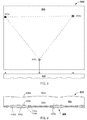
- FIG. 3 schematically illustrates a top or bottom view 302 of an example substrate layer of a multilayer substrate for semiconductor packaging 300, in accordance with some embodiments.
- the embodiment of FIG. 3 may comport with embodiments of substrate 100 of FIG. 1 and second layer 200 of FIG. 2 , while showing a top or bottom view 302 of an example substrate.
- the top or bottom view 302 of a substrate 300 of FIG. 3 may correspond to the first side 102a or the second side 102b of FIG. 1 .
- the three highest points 302a, 302b, 302c on the first side 102a may be spaced apart at different individual locations not in the same cross-section of the substrate 100, 300.
- the three highest points 302a, 302b, 302c on the second side 102b may be spaced apart at different individual locations not in the same cross-section of the substrate 100, 300.
- the individual locations of the three highest points 302a, 302b, 302c on first side 102a do not correspond to the individual locations of the three highest points 302a, 302b, 302c on the second side 102b, where 302a of the first side 102a does not correspond to 302a of the second side 102b, 302b of the first side 102a does not correspond to 302b of the second side 102b, and where 302c of the first side 102c does not correspond to 302c of the second side 102b.
- the individual location of a least one of the three highest points 302a, 302b, 302c on the first side 102a may correspond to the individual location of at least one of the three highest points 302a, 302b, 302c on the second side 102b.
- a planar view of 302 is shown in FIG. 3 where the three highest points 302a, 302b, 302c are shown as the highest points in the planar view and all other individual locations are shown in a single plane below the three highest points 302a, 302b, 302c.
- FIG. 4 schematically illustrates a cross-section side view of an example multilayer substrate for semiconductor packaging with selected electrical routing features illustrated 400, in accordance with some embodiments.
- the embodiment of FIG. 4 may comport with embodiments of the substrate 100 of FIG. 1 , the second layer 200 of FIG. 2 , and the substrate 300 of FIG. 3 , while showing selected electrical routing features.
- the first layer 102 has electrical routing features 400a, 400b (connections between 400a and 400b are not illustrated) to route electrical signals between the first side 102a of the first layer 102 and the second side 102b of the first layer 102, wherein the second layer 200 has electrical routing vias 400c electrically coupled to the electrical routing features of the second side 102b of the first layer 102 and passing through the second layer 200 from the first side 104a of the second layer 200 to the second side 104b of the second layer 200 connecting to a second side 104b feature 400d, wherein the electrical routing vias 400c have a depth corresponding to the thickness 200a of the second layer 200.
- FIG. 5 schematically illustrates a method of making a multilayer substrate for semiconductor packaging 500, in accordance with some embodiments.
- the embodiment of FIG. 5 may comport with embodiments of the substrate 100 of FIG. 1 , the second layer 200 of FIG. 2 , the substrate 300 of FIG. 3 , and the substrate 400 of FIG. 4 , with the addition of a method making a multilayer substrate.
- a first layer may be provided with a first side and a second side opposite the first side, wherein the first layer is unconstrained, wherein the first side may have a first side xy-plane defined by three highest points on the first side, and individual locations on the first side may have a first side distance below the first side xy-plane in a direction towards the second side, wherein the second side may have a second side xy-plane defined by three highest points on the second side, and individual locations on the second side may have a second side distance below the second side xy-plane in a direction towards the first side.
- the first layer may be constrained by flattening the first side of the first layer against a surface of a rigid vacuum plate to provide a constrained first layer, wherein the second side of the first layer may have a constrained second side distance that is the sum of the first side distance and the second side distance.
- a second layer may be coupled to the constrained first layer, the second layer with a first side coupled to the second side of the first layer and with a second side opposite the first side of the second layer, wherein a thickness of the second layer at the individual locations on the second layer may be comprised of the constrained second side distance, wherein a thickness of the first layer plus the thickness of the second layer at individual locations between the first side of the first layer and the second side of the second layer may be a substantially uniform thickness.
- the coupling of the second layer to the first layer may further comprise laminating, coating, or casting one or more layers of one or more dielectric materials.
- the coupling of the second layer to the first layer may further comprise laminating, wherein the laminating further comprises sequentially attaching, conformally pressing, and plate pressing three layers of ABF.
- the rigid vacuum plate may be removed from the first side of the first layer to provide an unconstrained multilayer substrate.
- FIG. 6 schematically illustrates a multilayer substrate for semiconductor packaging during various stages of fabrication 600, in accordance with some embodiments.
- the embodiment of FIG. 6 may comport with embodiments of the substrate 100 of FIG. 1 , the second layer 200 of FIG. 2 , the substrate 300 of FIG. 3 , the substrate 400 of FIG. 4 , and the method 500 of FIG. 5 , with the addition of multilayer substrates during various stages of fabrication.
- Structure 602 corresponds to 502 of method 500.
- Structure 602 illustrates a first layer 102 of a multilayer substrate as shown and described herein.
- first layer 102 may have a first side 102a and a second side 102b opposite the first side 102a, wherein the first side 102a may have a first side xy-plane 102c defined by three highest points on the first side 102a, and individual locations on the first side may have a first side distance 102d below the first side xy-plane 102c in a direction towards the second side 102b, wherein the second side 102b may have a second side xy-plane 102e defined by three highest points on the second side 102b, and individual locations on the second side 102b may have a second side distance 102f below the second side xy-plane 102e in a direction towards the first side 102a.
- Structure 604 corresponds to 504 of method 500.
- Structure 604 illustrates a first layer 102 that is constrained by a rigid flat vacuum plate 604b to provide a constrained first layer 604a.
- the constrained first layer may have first side 604c coupled to the rigid flat vacuum plate 604b and a second side 604d opposite the first side 604c.
- the first side distance 102d may translate to the second side 604d and provide a constrained second side distance 604e that is the sum of the first side distance 102d and the second side distance 102f.
- Structure 606 corresponds to 506 of method 500.
- Structure 606 illustrates the constrained first layer 604a with a second layer 606a coupled to the second side 604d.
- the thickness of the constrained first layer 604a plus the thickness of the second layer 606a at individual locations is a substantially uniform thickness 100a.
- Structure 608 corresponds to 508 of method 500. Structure 608 illustrates the first layer 102 (unconstrained) with the addition of the second layer 606a.
- FIGS. 5-6 Various operations of FIGS. 5-6 are described as multiple discrete operations in turn, in a manner that is most helpful in understanding the claimed subject matter. However, the order of description should not be construed as to imply that these operations are necessarily order dependent.
- FIG. 7 schematically illustrates a cross-section side view of a multilayer substrate for semiconductor packaging with a die attached to the substrate and selected electrical routing features illustrated (package) 700, in accordance with some embodiments.
- the embodiment of FIG. 7 may comport with embodiments of the substrate 100 of FIG. 1 , the second layer 200 of FIG. 2 , the substrate 300 of FIG. 3 , the substrate 400 of FIG. 4 , the method 500 of FIG. 5 , and the substrate of FIG. 6 , with the addition of a die attached to the substrate.
- package 700 may be comprised of a multilayer substrate 704 with a first layer 704a and a second layer 704b coupled to the first layer 704a.
- the first layer 704a may have a die 702 attached in a flip chip configuration to the first layer 704a.
- interconnects 702a may couple the die 702 to the first layer 704a.
- an underfill material may further couple the die 702 to the first layer 704a and may protect interconnects 702a.
- electrical routing features (not shown) may route electrical signals between the die 702 through the first layer 704a and second layer 704b to pads 704c on the second layer 704b.
- interconnects 706, such as solder balls, may be coupled to pads 704c for attachment to a board, such as a printed circuit board.
- the first layer 704a corresponds to the first layer 102 of the embodiment illustrated in FIG. 1 , except that the first layer 704a is constrained by die 702 coupled to the first layer 704a. Therefore, the first layer 704a is illustrated with a flat first side 704d in contrast to first side 102a of first layer 102 in an unconstrained condition.
- Second side 704e is illustrated to be not flat because first layer 704a is constrained by the die 702 coupled thereto.
- Second layer 704b is illustrated to be coupled to the first layer 704a and to follow the contour of the second side 704e of the first layer 704a.
- the opposite side of second layer 704b with interconnects 706 is illustrated to be flat since the die 702 constrains substrate 704.
- die 702 may have an underfill material 702b.
- FIG. 8 schematically illustrates a computing device that includes a multilayer substrate for semiconductor packaging as described herein, in accordance with some embodiments.
- the embodiment of FIG. 8 may comport with embodiments of the substrate 100 of FIG. 1 , the second layer 200 of FIG. 2 , the substrate 300 of FIG. 3 , the substrate 400 of FIG. 4 , the method 500 of FIG. 5 , the substrate of FIG. 6 , and the package 700 of FIG. 7 , with the addition of the multilayer substrate in a computing device.
- the substrate 100 of FIG. 1 may have a die coupled to the first side 102a in a flip chip configuration to provide a package 700 of FIG. 7 .
- the die may be a processor or memory.
- the package with the processor or memory may be coupled to the motherboard 802 of FIG. 8 .
- the computing device 800 may house a board such as motherboard 802 (e.g., in housing 826).
- the motherboard 802 may include a number of components, including but not limited to a processor 804, chipset 810, memory 812, slots 814, computer bus interface 816, LAN controller 818, and ports 820.
- the chipset 810 may include a communications chip.
- the components may be physically and electrically coupled to the motherboard 802 and may include other components.
- the term "processor" may refer to any device or portion of a device that processes electronic data from registers and/or memory to transform that electronic data into other electronic data that may be stored in registers and/or memory.
- the computing device 800 may include external devices 822 and interface devices 824 that may or may not be physically and electrically coupled to the motherboard 802. These other components may include, but are not limited to, a liquid cooling system, interface devices (keyboard, display, mouse), memory, a graphics processor, a digital signal processor, a crypto processor, a chipset, an antenna, a touchscreen display, a touchscreen controller, a battery, an audio codec, a video codec, a power amplifier, a global positioning system (GPS) device, a compass, a Geiger counter, an accelerometer, a gyroscope, a speaker, a camera, and a mass storage device (such as hard disk drive, compact disk (CD), digital versatile disk (DVD), and so forth).
- the computing device 800 may be a computer system, a server, a rack server, a blade server, and a super computer system. In further implementations, the computing device 800 may be any other electronic device that processes data.
- the present disclosure describes a multilayer substrate for semiconductor packaging .
Landscapes
- Engineering & Computer Science (AREA)
- Microelectronics & Electronic Packaging (AREA)
- Manufacturing & Machinery (AREA)
- Production Of Multi-Layered Print Wiring Board (AREA)
- Theoretical Computer Science (AREA)
- Physics & Mathematics (AREA)
- Computer Hardware Design (AREA)
- Human Computer Interaction (AREA)
- General Engineering & Computer Science (AREA)
- General Physics & Mathematics (AREA)
- Geometry (AREA)
- Structure Of Printed Boards (AREA)
Claims (10)
- Mehrschichtiges Substrat (100) für eine Halbleiterverkapselung, Folgendes umfassend:eine erste Schicht (102) mit einer ersten Seite (102a) und mit einer zweiten Seite (102b), die der ersten Seite entgegengesetzt ist, wobei die erste Seite eine xy-Ebene der ersten Seite (102c) aufweist, die durch drei höchste Punkte auf der ersten Seite definiert ist, und einzelne Orte auf der ersten Seite eine erste Seitenentfernung (102d) unter der xy-Ebene der ersten Seite in eine Richtung auf die zweite Seite aufweisen, wobei die zweite Seite eine xy-Ebene der zweiten Seite (102e) aufweist, die durch drei höchste Punkte auf der zweiten Seite definiert ist, und einzelne Orte auf der zweiten Seite eine zweite Seitenentfernung (102f) unter der xy-Ebene der zweiten Seite in eine Richtung auf die ersten Seite aufweisen; undeine zweite Schicht (104), die eine oder mehrere Schichten eines oder mehrerer dielektrischer Materialien mit einer ersten Seite (104a), die mit der zweiten Seite der ersten Schicht gekoppelt ist, und mit einer zweiten Seite (104b) umfasst, die der ersten Seite der zweiten Schicht entgegengesetzt ist, wobei eine Dicke (104c) der zweiten Schicht an einzelnen Orten auf der zweiten Schicht die erste Seitenentfernung plus die zweite Seitenentfernung umfasst, wobei eine Dicke der ersten Schicht plus die Dicke der zweiten Schicht an einzelnen Orten zwischen der ersten Seite der ersten Schicht und der zweiten Seite der zweiten Schicht eine im Wesentlichen gleichmäßige Dicke (100a) ist.
- Substrat nach Anspruch 1, wobei die erste Schicht elektrische Weglenkungsmerkmale (400a, 400b) aufweist, um elektrische Signale zwischen der ersten Seite der ersten Schicht und der zweiten Seite der ersten Schicht zu lenken, wobei die zweite Schicht elektrische Weglenkungskontaktlöcher (400c) aufweist, die elektrisch mit den elektrischen Weglenkungsmerkmalen der zweiten Seite der ersten Schicht verbunden sind und von der ersten Seite der zweiten Schicht zu der zweiten Seite der zweiten Schicht durch die zweite Schicht hindurch gehen, wobei die elektrischen Weglenkungskontaktlöcher eine Tiefe aufweisen, die der Dicke der zweiten Schicht entspricht.
- Substrat nach Anspruch 1, wobei die dielektrischen Materialien ein Polymer oder einen Polymerverbundstoff umfassen.
- Substrat nach Anspruch 3, wobei die dielektrischen Materialien aus der Gruppe ausgewählt sind, bestehend aus Ajinomoto Build-up Film (ABF), Feuerschutzmaterial 2 (FR2), Feuerschutzmaterial 4 (FR4), Polyimid, Passivierungsfilm (WPR), Polybenzthiazol (PBZT), Polybenzoxazol (PBO) und Formmasse und Kombinationen davon.
- Substrat nach Anspruch 1, wobei die Dicke der zweiten Schicht an den einzelnen Orten auf der zweiten Schicht die erste Seitenentfernung plus die zweite Seitenentfernung plus eine Versatzentfernung umfasst, wobei die Versatzentfernung kleiner ist als ungefähr zweimal die Summe der ersten Seitenentfernung und der zweiten Seitenentfernung.
- Substrat nach Anspruch 1, wobei die erste Schicht ein mehrschichtiges Verbundstoffsubstrat mit einem Kern ist.
- Verfahren zum Herstellen eines mehrschichtigen Substrats für eine Halbleiterverkapselung, das Verfahren Folgendes umfassend:Bereitstellen (502) einer ersten Schicht mit einer ersten Seite und mit einer zweiten Seite, die der ersten Seite entgegengesetzt ist, wobei die erste Seite eine xy-Ebene der ersten Seite aufweist, die durch drei höchste Punkte auf der ersten Seite definiert ist, und einzelne Orte auf der ersten Seite eine erste Seitenentfernung unter der xy-Ebene der ersten Seite in eine Richtung auf die zweite Seite aufweisen, wobei die zweite Seite eine xy-Ebene der zweiten Seite aufweist, die durch drei höchste Punkte auf der zweiten Seite definiert ist, und einzelne Orte auf der zweiten Seite eine zweite Seitenentfernung unter der xy-Ebene der zweiten Seite in eine Richtung auf die ersten Seite aufweisen;Einspannen (504) der ersten Schicht durch Plätten der ersten Seite der ersten Schicht gegen eine Oberfläche einer starren Vakuumplatte, um eine eingespannte erste Schicht bereitzustellen, wobei die zweite Seite der ersten Schicht eine eingespannte zweite Seitenentfernung aufweist, welche die Summe der ersten Seitenentfernung und der zweiten Seitenentfernung ist; undKoppeln (506) einer zweiten Schicht mit der eingespannten ersten Schicht, wobei die zweite Schicht eine oder mehrere Schichten eines oder mehrerer dielektrischer Materialien mit einer ersten Seite umfasst, die mit der zweiten Seite der ersten Schicht und mit einer zweiten Seite gekoppelt ist, die der ersten Seite der zweiten Schicht entgegengesetzt ist, wobei eine Dicke der zweiten Schicht an einzelnen Orten auf der zweiten Schicht die eingespannte zweite Seitenentfernung umfasst, so dass eine Dicke der ersten Schicht plus die Dicke der zweiten Schicht an einzelnen Orten zwischen der ersten Seite der ersten Schicht und der zweiten Seite der zweiten Schicht eine im Wesentlichen gleichmäßige Dicke ist.
- Verfahren nach Anspruch 7, wobei das Koppeln der zweiten Schicht mit der ersten Schicht weiterhin Folgendes umfasst:
Laminieren, Beschichten oder Gießen einer oder mehrerer Schichten eines oder mehrerer dielektrischer Materialien. - Verfahren nach Anspruch 8, wobei das Koppeln der zweiten Schicht mit der ersten Schicht Laminieren umfasst, wobei das Laminieren weiterhin Folgendes umfasst:
sequenzielles Befestigen, gleichförmiges Pressen und Plattenpressen von drei Aufbauschichten. - Verfahren nach Anspruch 9, weiterhin Folgendes umfassend:
Entfernen (508) der starren Vakuumplatte von der ersten Seite der ersten Schicht, um ein nicht eingespanntes mehrschichtiges Substrat bereitzustellen.
Applications Claiming Priority (1)
| Application Number | Priority Date | Filing Date | Title |
|---|---|---|---|
| PCT/US2014/071994 WO2016105349A1 (en) | 2014-12-22 | 2014-12-22 | Multilayer substrate for semiconductor packaging |
Publications (3)
| Publication Number | Publication Date |
|---|---|
| EP3055882A1 EP3055882A1 (de) | 2016-08-17 |
| EP3055882A4 EP3055882A4 (de) | 2018-02-14 |
| EP3055882B1 true EP3055882B1 (de) | 2020-09-16 |
Family
ID=55725047
Family Applications (1)
| Application Number | Title | Priority Date | Filing Date |
|---|---|---|---|
| EP14891614.1A Active EP3055882B1 (de) | 2014-12-22 | 2014-12-22 | Mehrschichtiges substrat für eine halbleiterverkapselung und verfahrren |
Country Status (8)
| Country | Link |
|---|---|
| US (1) | US9788416B2 (de) |
| EP (1) | EP3055882B1 (de) |
| JP (1) | JP6105178B2 (de) |
| KR (1) | KR101782347B1 (de) |
| CN (1) | CN105518858B (de) |
| BR (1) | BR112015029057A2 (de) |
| TW (1) | TWI603437B (de) |
| WO (1) | WO2016105349A1 (de) |
Families Citing this family (4)
| Publication number | Priority date | Publication date | Assignee | Title |
|---|---|---|---|---|
| US10217729B2 (en) | 2016-09-30 | 2019-02-26 | Intel Corporation | Apparatus for micro pick and bond |
| US20180166294A1 (en) * | 2016-12-13 | 2018-06-14 | Intel Corporation | Apparatus and methods to achieve uniform package thickness |
| CN110505767B (zh) * | 2019-07-08 | 2021-03-30 | 苏州固泰新材股份有限公司 | 一种软性铜箔基材及其制备方法 |
| WO2022030178A1 (ja) * | 2020-08-03 | 2022-02-10 | 株式会社村田製作所 | 構造体およびその製造方法 |
Family Cites Families (20)
| Publication number | Priority date | Publication date | Assignee | Title |
|---|---|---|---|---|
| US6177728B1 (en) * | 1998-04-28 | 2001-01-23 | International Business Machines Corporation | Integrated circuit chip device having balanced thermal expansion |
| JP2000022328A (ja) * | 1998-06-26 | 2000-01-21 | Sumitomo Metal Electronics Devices Inc | 多層配線用プリント基板の製造方法 |
| JP3637594B2 (ja) * | 2000-04-12 | 2005-04-13 | 信越半導体株式会社 | 半導体ウェーハの製造方法 |
| JP2002124763A (ja) * | 2000-10-16 | 2002-04-26 | Matsushita Electric Ind Co Ltd | 回路形成基板の製造方法、回路形成基板および回路形成基板用材料 |
| JP2002134375A (ja) * | 2000-10-25 | 2002-05-10 | Canon Inc | 半導体基体とその作製方法、および貼り合わせ基体の表面形状測定方法 |
| DE10115871B4 (de) * | 2001-03-30 | 2005-06-09 | Robert Bosch Gmbh | Verfahren zur Planarisierung von Schaumstoffoberflächen, Schaumstoffträger mit planarisierter Oberfläche und dessen Verwendung für Hochfrequenzschaltungen |
| JP3856733B2 (ja) * | 2002-06-27 | 2006-12-13 | 日本特殊陶業株式会社 | 配線基板の製造方法 |
| TW564533B (en) * | 2002-10-08 | 2003-12-01 | Siliconware Precision Industries Co Ltd | Warpage-preventing substrate |
| JP4741822B2 (ja) * | 2004-09-02 | 2011-08-10 | ルネサスエレクトロニクス株式会社 | 半導体装置の製造方法 |
| WO2006112474A2 (ja) * | 2005-04-19 | 2006-10-26 | Kaneka Corporation | 繊維-樹脂複合体、積層体、およびプリント配線板、並びにプリント配線板の製造方法 |
| JP2008027992A (ja) * | 2006-07-18 | 2008-02-07 | Lasertec Corp | Euvlマスク用基板の製造方法及びその基板を用いたeuvlマスクの製造方法 |
| KR100946374B1 (ko) * | 2008-04-29 | 2010-03-08 | 삼성전기주식회사 | 인쇄회로기판 및 그 제조방법 |
| JP2010122304A (ja) * | 2008-11-17 | 2010-06-03 | Dainippon Printing Co Ltd | 反射型マスクブランクス、反射型マスク、反射型マスクブランクスの製造方法、および、反射型マスクの製造方法 |
| US20110024899A1 (en) | 2009-07-28 | 2011-02-03 | Kenji Masumoto | Substrate structure for cavity package |
| US9401330B1 (en) * | 2009-10-13 | 2016-07-26 | Altera Corporation | IC package with non-uniform dielectric layer thickness |
| KR101096039B1 (ko) * | 2009-11-09 | 2011-12-19 | 주식회사 하이닉스반도체 | 인쇄회로기판 및 이를 이용한 반도체 패키지 |
| US20140252632A1 (en) * | 2013-03-06 | 2014-09-11 | Hans-Joachim Barth | Semiconductor devices |
| CN103391681B (zh) * | 2013-08-06 | 2016-12-28 | 上海美维电子有限公司 | 印刷线路板及其制造方法 |
| US9184139B2 (en) * | 2013-12-17 | 2015-11-10 | Stats Chippac, Ltd. | Semiconductor device and method of reducing warpage using a silicon to encapsulant ratio |
| US20150206812A1 (en) * | 2014-01-23 | 2015-07-23 | Qualcomm Incorporated | Substrate and method of forming the same |
-
2014
- 2014-12-22 CN CN201480026806.6A patent/CN105518858B/zh not_active Expired - Fee Related
- 2014-12-22 WO PCT/US2014/071994 patent/WO2016105349A1/en not_active Ceased
- 2014-12-22 EP EP14891614.1A patent/EP3055882B1/de active Active
- 2014-12-22 US US14/778,987 patent/US9788416B2/en not_active Expired - Fee Related
- 2014-12-22 KR KR1020157033254A patent/KR101782347B1/ko not_active Expired - Fee Related
- 2014-12-22 BR BR112015029057A patent/BR112015029057A2/pt not_active Application Discontinuation
- 2014-12-22 JP JP2016566845A patent/JP6105178B2/ja active Active
-
2015
- 2015-11-20 TW TW104138591A patent/TWI603437B/zh not_active IP Right Cessation
Non-Patent Citations (1)
| Title |
|---|
| None * |
Also Published As
| Publication number | Publication date |
|---|---|
| JP6105178B2 (ja) | 2017-03-29 |
| CN105518858B (zh) | 2019-02-22 |
| BR112015029057A2 (pt) | 2017-09-26 |
| TWI603437B (zh) | 2017-10-21 |
| EP3055882A4 (de) | 2018-02-14 |
| US20160329274A1 (en) | 2016-11-10 |
| KR101782347B1 (ko) | 2017-09-27 |
| TW201637142A (zh) | 2016-10-16 |
| US9788416B2 (en) | 2017-10-10 |
| EP3055882A1 (de) | 2016-08-17 |
| JP2017505550A (ja) | 2017-02-16 |
| CN105518858A (zh) | 2016-04-20 |
| KR20160089273A (ko) | 2016-07-27 |
| WO2016105349A1 (en) | 2016-06-30 |
Similar Documents
| Publication | Publication Date | Title |
|---|---|---|
| KR101754843B1 (ko) | 집적 회로 패키지 기판 | |
| US9716067B2 (en) | Integrated circuit package with embedded bridge | |
| CN103999215B (zh) | 用于微电子管芯、含有微电子管芯的微电子组件、微电子系统的封装,以及降低微电子封装中的管芯应力的方法 | |
| EP3295482B1 (de) | Verpackung mit zweischichtiger dielektrischer struktur | |
| US10205292B2 (en) | Socket contact techniques and configurations | |
| KR20210071818A (ko) | 재구성된 웨이퍼 조립체 | |
| US9842832B2 (en) | High density interconnection of microelectronic devices | |
| US20150255411A1 (en) | Die-to-die bonding and associated package configurations | |
| KR20200135165A (ko) | 다이들에 대한 인터커넥트 허브 | |
| US9788416B2 (en) | Multilayer substrate for semiconductor packaging | |
| EP2956962A1 (de) | Halbleiterbauelement mit gestapelten speicherelementen und verfahren zum stapeln von speicherelementen auf einem halbleiterbauelement | |
| US9601464B2 (en) | Thermally enhanced package-on-package structure | |
| US20140376195A1 (en) | Methods of forming dual sided coreless package structures with land side capacitor | |
| US20260090431A1 (en) | Glass etch protection and seware reduction by coating protection |
Legal Events
| Date | Code | Title | Description |
|---|---|---|---|
| PUAI | Public reference made under article 153(3) epc to a published international application that has entered the european phase |
Free format text: ORIGINAL CODE: 0009012 |
|
| 17P | Request for examination filed |
Effective date: 20151116 |
|
| AK | Designated contracting states |
Kind code of ref document: A1 Designated state(s): AL AT BE BG CH CY CZ DE DK EE ES FI FR GB GR HR HU IE IS IT LI LT LU LV MC MK MT NL NO PL PT RO RS SE SI SK SM TR |
|
| AX | Request for extension of the european patent |
Extension state: BA ME |
|
| RIC1 | Information provided on ipc code assigned before grant |
Ipc: H05K 1/03 20060101ALI20180103BHEP Ipc: H05K 1/11 20060101ALI20180103BHEP Ipc: H01L 25/065 20060101AFI20180103BHEP Ipc: H05K 3/00 20060101ALI20180103BHEP |
|
| A4 | Supplementary search report drawn up and despatched |
Effective date: 20180111 |
|
| DAX | Request for extension of the european patent (deleted) | ||
| RIC1 | Information provided on ipc code assigned before grant |
Ipc: H01L 25/065 20060101ALN20191218BHEP Ipc: H05K 1/11 20060101ALI20191218BHEP Ipc: H05K 1/03 20060101AFI20191218BHEP Ipc: H05K 3/00 20060101ALI20191218BHEP Ipc: H05K 1/02 20060101ALN20191218BHEP Ipc: H05K 1/18 20060101ALN20191218BHEP |
|
| RIC1 | Information provided on ipc code assigned before grant |
Ipc: H05K 1/02 20060101ALN20200123BHEP Ipc: H01L 25/065 20060101ALN20200123BHEP Ipc: H05K 1/11 20060101ALI20200123BHEP Ipc: H05K 1/18 20060101ALN20200123BHEP Ipc: H05K 3/00 20060101ALI20200123BHEP Ipc: H05K 1/03 20060101AFI20200123BHEP |
|
| RIC1 | Information provided on ipc code assigned before grant |
Ipc: H05K 1/03 20060101AFI20200127BHEP Ipc: H05K 1/18 20060101ALN20200127BHEP Ipc: H01L 25/065 20060101ALN20200127BHEP Ipc: H05K 1/02 20060101ALN20200127BHEP Ipc: H05K 1/11 20060101ALI20200127BHEP Ipc: H05K 3/00 20060101ALI20200127BHEP |
|
| GRAP | Despatch of communication of intention to grant a patent |
Free format text: ORIGINAL CODE: EPIDOSNIGR1 |
|
| STAA | Information on the status of an ep patent application or granted ep patent |
Free format text: STATUS: GRANT OF PATENT IS INTENDED |
|
| GRAJ | Information related to disapproval of communication of intention to grant by the applicant or resumption of examination proceedings by the epo deleted |
Free format text: ORIGINAL CODE: EPIDOSDIGR1 |
|
| REG | Reference to a national code |
Ref country code: DE Ref legal event code: R079 Ref document number: 602014070355 Country of ref document: DE Free format text: PREVIOUS MAIN CLASS: H01L0025065000 Ipc: H05K0001030000 |
|
| GRAP | Despatch of communication of intention to grant a patent |
Free format text: ORIGINAL CODE: EPIDOSNIGR1 |
|
| RIC1 | Information provided on ipc code assigned before grant |
Ipc: H05K 1/02 20060101ALN20200302BHEP Ipc: H05K 1/18 20060101ALN20200302BHEP Ipc: H01L 25/065 20060101ALN20200302BHEP Ipc: H05K 1/03 20060101AFI20200302BHEP Ipc: H05K 1/11 20060101ALI20200302BHEP Ipc: H05K 3/00 20060101ALI20200302BHEP |
|
| INTG | Intention to grant announced |
Effective date: 20200327 |
|
| INTG | Intention to grant announced |
Effective date: 20200407 |
|
| RAP1 | Party data changed (applicant data changed or rights of an application transferred) |
Owner name: INTEL CORPORATION |
|
| RIC1 | Information provided on ipc code assigned before grant |
Ipc: H05K 1/11 20060101ALI20200330BHEP Ipc: H01L 25/065 20060101ALN20200330BHEP Ipc: H05K 1/02 20060101ALN20200330BHEP Ipc: H05K 1/03 20060101AFI20200330BHEP Ipc: H05K 3/00 20060101ALI20200330BHEP Ipc: H05K 1/18 20060101ALN20200330BHEP |
|
| GRAS | Grant fee paid |
Free format text: ORIGINAL CODE: EPIDOSNIGR3 |
|
| GRAA | (expected) grant |
Free format text: ORIGINAL CODE: 0009210 |
|
| STAA | Information on the status of an ep patent application or granted ep patent |
Free format text: STATUS: THE PATENT HAS BEEN GRANTED |
|
| AK | Designated contracting states |
Kind code of ref document: B1 Designated state(s): AL AT BE BG CH CY CZ DE DK EE ES FI FR GB GR HR HU IE IS IT LI LT LU LV MC MK MT NL NO PL PT RO RS SE SI SK SM TR |
|
| REG | Reference to a national code |
Ref country code: GB Ref legal event code: FG4D |
|
| REG | Reference to a national code |
Ref country code: CH Ref legal event code: EP |
|
| REG | Reference to a national code |
Ref country code: DE Ref legal event code: R096 Ref document number: 602014070355 Country of ref document: DE |
|
| REG | Reference to a national code |
Ref country code: IE Ref legal event code: FG4D |
|
| REG | Reference to a national code |
Ref country code: AT Ref legal event code: REF Ref document number: 1315393 Country of ref document: AT Kind code of ref document: T Effective date: 20201015 |
|
| REG | Reference to a national code |
Ref country code: NL Ref legal event code: FP |
|
| PG25 | Lapsed in a contracting state [announced via postgrant information from national office to epo] |
Ref country code: SE Free format text: LAPSE BECAUSE OF FAILURE TO SUBMIT A TRANSLATION OF THE DESCRIPTION OR TO PAY THE FEE WITHIN THE PRESCRIBED TIME-LIMIT Effective date: 20200916 Ref country code: BG Free format text: LAPSE BECAUSE OF FAILURE TO SUBMIT A TRANSLATION OF THE DESCRIPTION OR TO PAY THE FEE WITHIN THE PRESCRIBED TIME-LIMIT Effective date: 20201216 Ref country code: HR Free format text: LAPSE BECAUSE OF FAILURE TO SUBMIT A TRANSLATION OF THE DESCRIPTION OR TO PAY THE FEE WITHIN THE PRESCRIBED TIME-LIMIT Effective date: 20200916 Ref country code: NO Free format text: LAPSE BECAUSE OF FAILURE TO SUBMIT A TRANSLATION OF THE DESCRIPTION OR TO PAY THE FEE WITHIN THE PRESCRIBED TIME-LIMIT Effective date: 20201216 Ref country code: GR Free format text: LAPSE BECAUSE OF FAILURE TO SUBMIT A TRANSLATION OF THE DESCRIPTION OR TO PAY THE FEE WITHIN THE PRESCRIBED TIME-LIMIT Effective date: 20201217 Ref country code: FI Free format text: LAPSE BECAUSE OF FAILURE TO SUBMIT A TRANSLATION OF THE DESCRIPTION OR TO PAY THE FEE WITHIN THE PRESCRIBED TIME-LIMIT Effective date: 20200916 |
|
| PGFP | Annual fee paid to national office [announced via postgrant information from national office to epo] |
Ref country code: GB Payment date: 20201209 Year of fee payment: 7 Ref country code: FR Payment date: 20201125 Year of fee payment: 7 |
|
| REG | Reference to a national code |
Ref country code: AT Ref legal event code: MK05 Ref document number: 1315393 Country of ref document: AT Kind code of ref document: T Effective date: 20200916 |
|
| PG25 | Lapsed in a contracting state [announced via postgrant information from national office to epo] |
Ref country code: RS Free format text: LAPSE BECAUSE OF FAILURE TO SUBMIT A TRANSLATION OF THE DESCRIPTION OR TO PAY THE FEE WITHIN THE PRESCRIBED TIME-LIMIT Effective date: 20200916 Ref country code: LV Free format text: LAPSE BECAUSE OF FAILURE TO SUBMIT A TRANSLATION OF THE DESCRIPTION OR TO PAY THE FEE WITHIN THE PRESCRIBED TIME-LIMIT Effective date: 20200916 |
|
| PGFP | Annual fee paid to national office [announced via postgrant information from national office to epo] |
Ref country code: NL Payment date: 20201214 Year of fee payment: 7 |
|
| REG | Reference to a national code |
Ref country code: LT Ref legal event code: MG4D |
|
| PG25 | Lapsed in a contracting state [announced via postgrant information from national office to epo] |
Ref country code: SM Free format text: LAPSE BECAUSE OF FAILURE TO SUBMIT A TRANSLATION OF THE DESCRIPTION OR TO PAY THE FEE WITHIN THE PRESCRIBED TIME-LIMIT Effective date: 20200916 Ref country code: RO Free format text: LAPSE BECAUSE OF FAILURE TO SUBMIT A TRANSLATION OF THE DESCRIPTION OR TO PAY THE FEE WITHIN THE PRESCRIBED TIME-LIMIT Effective date: 20200916 Ref country code: EE Free format text: LAPSE BECAUSE OF FAILURE TO SUBMIT A TRANSLATION OF THE DESCRIPTION OR TO PAY THE FEE WITHIN THE PRESCRIBED TIME-LIMIT Effective date: 20200916 Ref country code: LT Free format text: LAPSE BECAUSE OF FAILURE TO SUBMIT A TRANSLATION OF THE DESCRIPTION OR TO PAY THE FEE WITHIN THE PRESCRIBED TIME-LIMIT Effective date: 20200916 Ref country code: PT Free format text: LAPSE BECAUSE OF FAILURE TO SUBMIT A TRANSLATION OF THE DESCRIPTION OR TO PAY THE FEE WITHIN THE PRESCRIBED TIME-LIMIT Effective date: 20210118 Ref country code: CZ Free format text: LAPSE BECAUSE OF FAILURE TO SUBMIT A TRANSLATION OF THE DESCRIPTION OR TO PAY THE FEE WITHIN THE PRESCRIBED TIME-LIMIT Effective date: 20200916 |
|
| PG25 | Lapsed in a contracting state [announced via postgrant information from national office to epo] |
Ref country code: AL Free format text: LAPSE BECAUSE OF FAILURE TO SUBMIT A TRANSLATION OF THE DESCRIPTION OR TO PAY THE FEE WITHIN THE PRESCRIBED TIME-LIMIT Effective date: 20200916 Ref country code: AT Free format text: LAPSE BECAUSE OF FAILURE TO SUBMIT A TRANSLATION OF THE DESCRIPTION OR TO PAY THE FEE WITHIN THE PRESCRIBED TIME-LIMIT Effective date: 20200916 Ref country code: ES Free format text: LAPSE BECAUSE OF FAILURE TO SUBMIT A TRANSLATION OF THE DESCRIPTION OR TO PAY THE FEE WITHIN THE PRESCRIBED TIME-LIMIT Effective date: 20200916 Ref country code: IS Free format text: LAPSE BECAUSE OF FAILURE TO SUBMIT A TRANSLATION OF THE DESCRIPTION OR TO PAY THE FEE WITHIN THE PRESCRIBED TIME-LIMIT Effective date: 20210116 Ref country code: PL Free format text: LAPSE BECAUSE OF FAILURE TO SUBMIT A TRANSLATION OF THE DESCRIPTION OR TO PAY THE FEE WITHIN THE PRESCRIBED TIME-LIMIT Effective date: 20200916 |
|
| REG | Reference to a national code |
Ref country code: DE Ref legal event code: R097 Ref document number: 602014070355 Country of ref document: DE |
|
| PG25 | Lapsed in a contracting state [announced via postgrant information from national office to epo] |
Ref country code: SK Free format text: LAPSE BECAUSE OF FAILURE TO SUBMIT A TRANSLATION OF THE DESCRIPTION OR TO PAY THE FEE WITHIN THE PRESCRIBED TIME-LIMIT Effective date: 20200916 |
|
| PLBE | No opposition filed within time limit |
Free format text: ORIGINAL CODE: 0009261 |
|
| STAA | Information on the status of an ep patent application or granted ep patent |
Free format text: STATUS: NO OPPOSITION FILED WITHIN TIME LIMIT |
|
| REG | Reference to a national code |
Ref country code: CH Ref legal event code: PL |
|
| 26N | No opposition filed |
Effective date: 20210617 |
|
| PG25 | Lapsed in a contracting state [announced via postgrant information from national office to epo] |
Ref country code: SI Free format text: LAPSE BECAUSE OF FAILURE TO SUBMIT A TRANSLATION OF THE DESCRIPTION OR TO PAY THE FEE WITHIN THE PRESCRIBED TIME-LIMIT Effective date: 20200916 Ref country code: MC Free format text: LAPSE BECAUSE OF FAILURE TO SUBMIT A TRANSLATION OF THE DESCRIPTION OR TO PAY THE FEE WITHIN THE PRESCRIBED TIME-LIMIT Effective date: 20200916 Ref country code: DK Free format text: LAPSE BECAUSE OF FAILURE TO SUBMIT A TRANSLATION OF THE DESCRIPTION OR TO PAY THE FEE WITHIN THE PRESCRIBED TIME-LIMIT Effective date: 20200916 |
|
| REG | Reference to a national code |
Ref country code: BE Ref legal event code: MM Effective date: 20201231 |
|
| PG25 | Lapsed in a contracting state [announced via postgrant information from national office to epo] |
Ref country code: LU Free format text: LAPSE BECAUSE OF NON-PAYMENT OF DUE FEES Effective date: 20201222 Ref country code: IT Free format text: LAPSE BECAUSE OF FAILURE TO SUBMIT A TRANSLATION OF THE DESCRIPTION OR TO PAY THE FEE WITHIN THE PRESCRIBED TIME-LIMIT Effective date: 20200916 Ref country code: IE Free format text: LAPSE BECAUSE OF NON-PAYMENT OF DUE FEES Effective date: 20201222 |
|
| PG25 | Lapsed in a contracting state [announced via postgrant information from national office to epo] |
Ref country code: LI Free format text: LAPSE BECAUSE OF NON-PAYMENT OF DUE FEES Effective date: 20201231 Ref country code: CH Free format text: LAPSE BECAUSE OF NON-PAYMENT OF DUE FEES Effective date: 20201231 |
|
| PG25 | Lapsed in a contracting state [announced via postgrant information from national office to epo] |
Ref country code: TR Free format text: LAPSE BECAUSE OF FAILURE TO SUBMIT A TRANSLATION OF THE DESCRIPTION OR TO PAY THE FEE WITHIN THE PRESCRIBED TIME-LIMIT Effective date: 20200916 Ref country code: MT Free format text: LAPSE BECAUSE OF FAILURE TO SUBMIT A TRANSLATION OF THE DESCRIPTION OR TO PAY THE FEE WITHIN THE PRESCRIBED TIME-LIMIT Effective date: 20200916 Ref country code: CY Free format text: LAPSE BECAUSE OF FAILURE TO SUBMIT A TRANSLATION OF THE DESCRIPTION OR TO PAY THE FEE WITHIN THE PRESCRIBED TIME-LIMIT Effective date: 20200916 |
|
| PG25 | Lapsed in a contracting state [announced via postgrant information from national office to epo] |
Ref country code: MK Free format text: LAPSE BECAUSE OF FAILURE TO SUBMIT A TRANSLATION OF THE DESCRIPTION OR TO PAY THE FEE WITHIN THE PRESCRIBED TIME-LIMIT Effective date: 20200916 |
|
| PG25 | Lapsed in a contracting state [announced via postgrant information from national office to epo] |
Ref country code: BE Free format text: LAPSE BECAUSE OF NON-PAYMENT OF DUE FEES Effective date: 20201231 |
|
| REG | Reference to a national code |
Ref country code: NL Ref legal event code: MM Effective date: 20220101 |
|
| GBPC | Gb: european patent ceased through non-payment of renewal fee |
Effective date: 20211222 |
|
| PG25 | Lapsed in a contracting state [announced via postgrant information from national office to epo] |
Ref country code: NL Free format text: LAPSE BECAUSE OF NON-PAYMENT OF DUE FEES Effective date: 20220101 |
|
| PG25 | Lapsed in a contracting state [announced via postgrant information from national office to epo] |
Ref country code: GB Free format text: LAPSE BECAUSE OF NON-PAYMENT OF DUE FEES Effective date: 20211222 |
|
| PG25 | Lapsed in a contracting state [announced via postgrant information from national office to epo] |
Ref country code: FR Free format text: LAPSE BECAUSE OF NON-PAYMENT OF DUE FEES Effective date: 20211231 |
|
| P01 | Opt-out of the competence of the unified patent court (upc) registered |
Effective date: 20230518 |
|
| PGFP | Annual fee paid to national office [announced via postgrant information from national office to epo] |
Ref country code: DE Payment date: 20241120 Year of fee payment: 11 |