EP3044809B1 - Boîtier à grille de connexions pour del à puce retournée - Google Patents
Boîtier à grille de connexions pour del à puce retournée Download PDFInfo
- Publication number
- EP3044809B1 EP3044809B1 EP14786296.5A EP14786296A EP3044809B1 EP 3044809 B1 EP3044809 B1 EP 3044809B1 EP 14786296 A EP14786296 A EP 14786296A EP 3044809 B1 EP3044809 B1 EP 3044809B1
- Authority
- EP
- European Patent Office
- Prior art keywords
- light emitting
- frame
- substrate
- light
- cap
- Prior art date
- Legal status (The legal status is an assumption and is not a legal conclusion. Google has not performed a legal analysis and makes no representation as to the accuracy of the status listed.)
- Active
Links
- 239000000758 substrate Substances 0.000 claims description 35
- 239000000463 material Substances 0.000 claims description 30
- 238000000034 method Methods 0.000 claims description 24
- 239000004065 semiconductor Substances 0.000 claims description 12
- 238000006243 chemical reaction Methods 0.000 claims description 11
- 239000000853 adhesive Substances 0.000 claims description 6
- 230000001070 adhesive effect Effects 0.000 claims description 6
- 229910052594 sapphire Inorganic materials 0.000 claims description 6
- 239000010980 sapphire Substances 0.000 claims description 6
- 230000003287 optical effect Effects 0.000 description 15
- 239000004020 conductor Substances 0.000 description 6
- 239000008393 encapsulating agent Substances 0.000 description 6
- 239000007788 liquid Substances 0.000 description 6
- 239000011248 coating agent Substances 0.000 description 3
- 238000000576 coating method Methods 0.000 description 3
- 238000000605 extraction Methods 0.000 description 3
- OAICVXFJPJFONN-UHFFFAOYSA-N Phosphorus Chemical compound [P] OAICVXFJPJFONN-UHFFFAOYSA-N 0.000 description 2
- GWEVSGVZZGPLCZ-UHFFFAOYSA-N Titan oxide Chemical compound O=[Ti]=O GWEVSGVZZGPLCZ-UHFFFAOYSA-N 0.000 description 2
- 230000001419 dependent effect Effects 0.000 description 2
- 238000005286 illumination Methods 0.000 description 2
- 238000003780 insertion Methods 0.000 description 2
- 230000037431 insertion Effects 0.000 description 2
- 238000004519 manufacturing process Methods 0.000 description 2
- 238000004806 packaging method and process Methods 0.000 description 2
- 229920001296 polysiloxane Polymers 0.000 description 2
- 239000011253 protective coating Substances 0.000 description 2
- JMASRVWKEDWRBT-UHFFFAOYSA-N Gallium nitride Chemical compound [Ga]#N JMASRVWKEDWRBT-UHFFFAOYSA-N 0.000 description 1
- BQCADISMDOOEFD-UHFFFAOYSA-N Silver Chemical compound [Ag] BQCADISMDOOEFD-UHFFFAOYSA-N 0.000 description 1
- 230000009286 beneficial effect Effects 0.000 description 1
- 230000002860 competitive effect Effects 0.000 description 1
- 230000008878 coupling Effects 0.000 description 1
- 238000010168 coupling process Methods 0.000 description 1
- 238000005859 coupling reaction Methods 0.000 description 1
- 238000005520 cutting process Methods 0.000 description 1
- 238000007598 dipping method Methods 0.000 description 1
- 238000009826 distribution Methods 0.000 description 1
- 238000005538 encapsulation Methods 0.000 description 1
- 239000012467 final product Substances 0.000 description 1
- 239000011521 glass Substances 0.000 description 1
- 238000009434 installation Methods 0.000 description 1
- 238000003698 laser cutting Methods 0.000 description 1
- 230000005693 optoelectronics Effects 0.000 description 1
- 238000012858 packaging process Methods 0.000 description 1
- 239000000047 product Substances 0.000 description 1
- 229910052709 silver Inorganic materials 0.000 description 1
- 239000004332 silver Substances 0.000 description 1
- 239000007921 spray Substances 0.000 description 1
- 239000010409 thin film Substances 0.000 description 1
Images


Classifications
-
- H—ELECTRICITY
- H01—ELECTRIC ELEMENTS
- H01L—SEMICONDUCTOR DEVICES NOT COVERED BY CLASS H10
- H01L33/00—Semiconductor devices with at least one potential-jump barrier or surface barrier specially adapted for light emission; Processes or apparatus specially adapted for the manufacture or treatment thereof or of parts thereof; Details thereof
- H01L33/48—Semiconductor devices with at least one potential-jump barrier or surface barrier specially adapted for light emission; Processes or apparatus specially adapted for the manufacture or treatment thereof or of parts thereof; Details thereof characterised by the semiconductor body packages
- H01L33/483—Containers
-
- H—ELECTRICITY
- H01—ELECTRIC ELEMENTS
- H01L—SEMICONDUCTOR DEVICES NOT COVERED BY CLASS H10
- H01L33/00—Semiconductor devices with at least one potential-jump barrier or surface barrier specially adapted for light emission; Processes or apparatus specially adapted for the manufacture or treatment thereof or of parts thereof; Details thereof
- H01L33/48—Semiconductor devices with at least one potential-jump barrier or surface barrier specially adapted for light emission; Processes or apparatus specially adapted for the manufacture or treatment thereof or of parts thereof; Details thereof characterised by the semiconductor body packages
- H01L33/58—Optical field-shaping elements
- H01L33/60—Reflective elements
-
- H—ELECTRICITY
- H01—ELECTRIC ELEMENTS
- H01L—SEMICONDUCTOR DEVICES NOT COVERED BY CLASS H10
- H01L25/00—Assemblies consisting of a plurality of individual semiconductor or other solid state devices ; Multistep manufacturing processes thereof
- H01L25/03—Assemblies consisting of a plurality of individual semiconductor or other solid state devices ; Multistep manufacturing processes thereof all the devices being of a type provided for in the same subgroup of groups H01L27/00 - H01L33/00, or in a single subclass of H10K, H10N, e.g. assemblies of rectifier diodes
- H01L25/04—Assemblies consisting of a plurality of individual semiconductor or other solid state devices ; Multistep manufacturing processes thereof all the devices being of a type provided for in the same subgroup of groups H01L27/00 - H01L33/00, or in a single subclass of H10K, H10N, e.g. assemblies of rectifier diodes the devices not having separate containers
- H01L25/075—Assemblies consisting of a plurality of individual semiconductor or other solid state devices ; Multistep manufacturing processes thereof all the devices being of a type provided for in the same subgroup of groups H01L27/00 - H01L33/00, or in a single subclass of H10K, H10N, e.g. assemblies of rectifier diodes the devices not having separate containers the devices being of a type provided for in group H01L33/00
- H01L25/0753—Assemblies consisting of a plurality of individual semiconductor or other solid state devices ; Multistep manufacturing processes thereof all the devices being of a type provided for in the same subgroup of groups H01L27/00 - H01L33/00, or in a single subclass of H10K, H10N, e.g. assemblies of rectifier diodes the devices not having separate containers the devices being of a type provided for in group H01L33/00 the devices being arranged next to each other
-
- H—ELECTRICITY
- H01—ELECTRIC ELEMENTS
- H01L—SEMICONDUCTOR DEVICES NOT COVERED BY CLASS H10
- H01L33/00—Semiconductor devices with at least one potential-jump barrier or surface barrier specially adapted for light emission; Processes or apparatus specially adapted for the manufacture or treatment thereof or of parts thereof; Details thereof
- H01L33/005—Processes
- H01L33/0062—Processes for devices with an active region comprising only III-V compounds
- H01L33/0075—Processes for devices with an active region comprising only III-V compounds comprising nitride compounds
-
- H—ELECTRICITY
- H01—ELECTRIC ELEMENTS
- H01L—SEMICONDUCTOR DEVICES NOT COVERED BY CLASS H10
- H01L33/00—Semiconductor devices with at least one potential-jump barrier or surface barrier specially adapted for light emission; Processes or apparatus specially adapted for the manufacture or treatment thereof or of parts thereof; Details thereof
- H01L33/48—Semiconductor devices with at least one potential-jump barrier or surface barrier specially adapted for light emission; Processes or apparatus specially adapted for the manufacture or treatment thereof or of parts thereof; Details thereof characterised by the semiconductor body packages
- H01L33/483—Containers
- H01L33/486—Containers adapted for surface mounting
-
- H—ELECTRICITY
- H01—ELECTRIC ELEMENTS
- H01L—SEMICONDUCTOR DEVICES NOT COVERED BY CLASS H10
- H01L33/00—Semiconductor devices with at least one potential-jump barrier or surface barrier specially adapted for light emission; Processes or apparatus specially adapted for the manufacture or treatment thereof or of parts thereof; Details thereof
- H01L33/48—Semiconductor devices with at least one potential-jump barrier or surface barrier specially adapted for light emission; Processes or apparatus specially adapted for the manufacture or treatment thereof or of parts thereof; Details thereof characterised by the semiconductor body packages
- H01L33/50—Wavelength conversion elements
- H01L33/501—Wavelength conversion elements characterised by the materials, e.g. binder
- H01L33/502—Wavelength conversion materials
-
- H—ELECTRICITY
- H01—ELECTRIC ELEMENTS
- H01L—SEMICONDUCTOR DEVICES NOT COVERED BY CLASS H10
- H01L2924/00—Indexing scheme for arrangements or methods for connecting or disconnecting semiconductor or solid-state bodies as covered by H01L24/00
- H01L2924/10—Details of semiconductor or other solid state devices to be connected
- H01L2924/11—Device type
- H01L2924/12—Passive devices, e.g. 2 terminal devices
- H01L2924/1204—Optical Diode
- H01L2924/12041—LED
-
- H—ELECTRICITY
- H01—ELECTRIC ELEMENTS
- H01L—SEMICONDUCTOR DEVICES NOT COVERED BY CLASS H10
- H01L2933/00—Details relating to devices covered by the group H01L33/00 but not provided for in its subgroups
- H01L2933/0008—Processes
- H01L2933/0033—Processes relating to semiconductor body packages
-
- H—ELECTRICITY
- H01—ELECTRIC ELEMENTS
- H01L—SEMICONDUCTOR DEVICES NOT COVERED BY CLASS H10
- H01L2933/00—Details relating to devices covered by the group H01L33/00 but not provided for in its subgroups
- H01L2933/0008—Processes
- H01L2933/0033—Processes relating to semiconductor body packages
- H01L2933/0041—Processes relating to semiconductor body packages relating to wavelength conversion elements
-
- H—ELECTRICITY
- H01—ELECTRIC ELEMENTS
- H01L—SEMICONDUCTOR DEVICES NOT COVERED BY CLASS H10
- H01L2933/00—Details relating to devices covered by the group H01L33/00 but not provided for in its subgroups
- H01L2933/0008—Processes
- H01L2933/0033—Processes relating to semiconductor body packages
- H01L2933/0058—Processes relating to semiconductor body packages relating to optical field-shaping elements
-
- H—ELECTRICITY
- H01—ELECTRIC ELEMENTS
- H01L—SEMICONDUCTOR DEVICES NOT COVERED BY CLASS H10
- H01L33/00—Semiconductor devices with at least one potential-jump barrier or surface barrier specially adapted for light emission; Processes or apparatus specially adapted for the manufacture or treatment thereof or of parts thereof; Details thereof
- H01L33/005—Processes
- H01L33/0095—Post-treatment of devices, e.g. annealing, recrystallisation or short-circuit elimination
-
- H—ELECTRICITY
- H01—ELECTRIC ELEMENTS
- H01L—SEMICONDUCTOR DEVICES NOT COVERED BY CLASS H10
- H01L33/00—Semiconductor devices with at least one potential-jump barrier or surface barrier specially adapted for light emission; Processes or apparatus specially adapted for the manufacture or treatment thereof or of parts thereof; Details thereof
- H01L33/48—Semiconductor devices with at least one potential-jump barrier or surface barrier specially adapted for light emission; Processes or apparatus specially adapted for the manufacture or treatment thereof or of parts thereof; Details thereof characterised by the semiconductor body packages
- H01L33/50—Wavelength conversion elements
-
- H—ELECTRICITY
- H01—ELECTRIC ELEMENTS
- H01L—SEMICONDUCTOR DEVICES NOT COVERED BY CLASS H10
- H01L33/00—Semiconductor devices with at least one potential-jump barrier or surface barrier specially adapted for light emission; Processes or apparatus specially adapted for the manufacture or treatment thereof or of parts thereof; Details thereof
- H01L33/48—Semiconductor devices with at least one potential-jump barrier or surface barrier specially adapted for light emission; Processes or apparatus specially adapted for the manufacture or treatment thereof or of parts thereof; Details thereof characterised by the semiconductor body packages
- H01L33/58—Optical field-shaping elements
-
- H—ELECTRICITY
- H01—ELECTRIC ELEMENTS
- H01L—SEMICONDUCTOR DEVICES NOT COVERED BY CLASS H10
- H01L33/00—Semiconductor devices with at least one potential-jump barrier or surface barrier specially adapted for light emission; Processes or apparatus specially adapted for the manufacture or treatment thereof or of parts thereof; Details thereof
- H01L33/48—Semiconductor devices with at least one potential-jump barrier or surface barrier specially adapted for light emission; Processes or apparatus specially adapted for the manufacture or treatment thereof or of parts thereof; Details thereof characterised by the semiconductor body packages
- H01L33/62—Arrangements for conducting electric current to or from the semiconductor body, e.g. lead-frames, wire-bonds or solder balls
Definitions
- This invention relates to the field of light emitting devices, and in particular to a frame that provides a reflective enclosure about the periphery of the device.
- An LED leadframe generally comprises a pair of conductors that are shaped to provide for external connections to the LED.
- a support frame may be molded about the leadframe such that the leadframe conductors provide conductive surfaces within the support frame to mount the LED, and conductive surfaces at the exterior of the support frame to mount the framed LED on a printed circuit board or other fixture.
- FIG. 7A illustrates two leadframes 16 within a molded frame array 40.
- Each leadframe 16 includes conductors 12 and 14.
- a tub 10 is formed about each leadframe 16, and the conductors 12 and 14 of leadframe 16 are shaped to extend through the frame element 40 so as to provide contacts 12a, 14a within the tub 10 for mounting a light emitting device, and contacts 12b, 14b for subsequent mounting of the tub 10 with light emitting device onto a printed circuit board or other fixture.
- a molded frame array 40 may include hundreds of leadframes 16 and tubs 10.
- FIG. 7B illustrates two light emitting modules 38.
- a light emitting device 20 which may be a thin-film device with minimal inherent structural support, is situated on a submount 30, which provides the necessary structural support to the light emitting device 20.
- Other devices such as an ESD protection device 26 may also be situated on the submount 30.
- a protective coating 28 may be provided upon the submount 30. Conductors 24 through the submount 30 couple the light emitting device 20 to the contacts 12 and 14 in the leadframe 16.
- the tub 10 may be subsequently filled with an encapsulant.
- the encapsulant, or the protective coating 28, or the light emitting device 20 may include a wavelength conversion material, such as phosphor, that absorbs some or all of the emitted light and emits light at a different wavelength.
- the interior walls 15 of the tub 10 may be reflective, to redirect light toward the outside of the tub 10.
- the individual light emitting modules 38 formed by the frame array 40 are singulated by slicing along the line 36.
- the individualized light emitting modules 38 include side surfaces 35 that facilitate the picking and placing of the light emitting module 38, but consume significantly more volume than the light-producing element 20, and introduces a substantially larger footprint compared to the surface area of the light-producing element 20. This substantial volume and footprint 'overhead' limits the use of such a light emitting module in applications such as flash or illumination elements for portable devices, such as smart phones and the like.
- US 2013/0032842 A1 refers to a light emitting device package, comprising a body part with a through hole, a light emitting device disposed within the through hole, and a wavelength conversion part.
- DE 10 2009 036 621 A1 refers to a method for producing an optoelectronic semiconductor element.
- a support and a semiconductor chip are surrounded by a forming element.
- WO 2007/147278 A2 refers to a LED light source for installation in flat elements with a connection board comprising contact areas.
- a hollow frame is configured to surround the periphery of a substantially self-supporting flip-chip light emitting device.
- the frame may be shaped to also contain a wavelength conversion element above the light emitting surface of the light emitting device.
- the lower surface of the light emitting device, which is exposed through the hollow frame, includes contact pads coupled to the light emitting element for surface mounting the light emitting module on a printed circuit board or other fixture.
- the flip-chip light emitting device may include a patterned sapphire substrate (PSS) upon which the light emitting element is grown, the patterned surface providing enhanced light extraction from the light emitting element, through the patterned sapphire growth substrate.
- PSS patterned sapphire substrate
- FIGs. 8A-8C illustrate an example of several self-supporting light emitting devices 100.
- FIG. 8A illustrates a substrate 110, upon which semiconductor layers are formed/grown to create multiple light emitting devices 100.
- the substrate 110 is commonly sapphire or glass, and the light emitting element 120 of each device 100 commonly includes an active region sandwiched between an n-type semiconductor layer and a p-type semiconductor layer. Pads 130 provide contact to the n and p layers, such that when current flows between these layers, light is emitted from the active region.
- Gallium nitride (GaN) doped to provide the n-type and p-type semiconductors, is commonly used as the semiconductor forming the light emitting element 120.
- the substrate 110 may be sliced/diced (dashed lines in FIG. 8A ) to provide singular light emitting chips 100.
- the individual light emitting chips are typically oriented in a 'flip-chip' configuration as illustrated in FIG. 8B , with the contact pads 130 on the nominal 'bottom' of the chip 100, as illustrated in FIG. 8C .
- Light is emitted primarily from the 'top' surface 125 of the light emitting element 120, into the substrate 110, and subsequently emitted from the top 115 and side 116 surfaces of the substrate 110. Some light may also be emitted from the side surface 126 of the light emitting element 120.
- the interface between the substrate 110 and light emitting element 120 may be 'roughened' to reduce the likelihood of total internal reflection (TIR) at the interface.
- the substrate 110 is a Patterned Sapphire Substrate (PSS) upon which the light emitting element 120 is grown, the pattern on the sapphire substrate creating the aforementioned 'roughened' interface between the substrate 110 and the light emitting element 120.
- PSS Patterned Sapphire Substrate
- the light emitting device 100 is substantially self-supporting, it generally may be 'packaged' to withstand subsequent handling as it undergoes the various processes during assembly of the final product, such as the assembly of a printed circuit board and other fixtures.
- the chips 100 may be placed on a strip or array of leadframes, with the pads 130 soldered to conductors in the leadframe that enable external connection to each of the light emitting chip 100.
- the array of leadframes is processed to encapsulate each of the light emitting chips, or sets of light emitting chips, then singulated to provide individual encapsulated ('packaged') light emitting devices.
- the encapsulation serves multiple purposes; the encapsulant protects the light emitting chip from the environment, and may be formed to provide one or more particular optical functions.
- the encapsulant may include wavelength conversion material, such as phosphor, that converts some or all of the light emitted from the light emitting chip 100 into light of a different wavelength.
- the encapsulant may also be shaped to form a lens that provides a desired light output pattern.
- the encapsulant may be placed within a well formed by reflective walls, such as the tub 10 of the light emitting module 38 in FIG. 7B .
- the present invention discloses a light emitting device according to claim 1 and the corresponding method of forming thereof according to claim 13. Further embodiments are disclosed in the dependent claims.
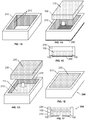
- FIGs. 1A-1F illustrate a packaging process that eliminates the need for a leadframe and provides for minimal volume and footprint overhead.
- FIG. 1A illustrates an example hollow frame 210, within which a light emitting chip may be placed.
- the interior walls 215 of the frame 210 may be reflective, using, for example, a coating of silver (Ag) or other reflective material.
- the shape and size of the opening in the frame 210 may correspond to the shape and size of the light emitting chip 100, as illustrated in FIG. 1B .
- the light emitting chip 100 is pre-tested, so that only operational chips 100 are packaged.
- FIGs. 1A-1F illustrate a single frame 210
- an array 400 of frames 210 such as illustrated in FIG. 4 , may be provided to enable simultaneous assembly and testing of multiple frames 210.
- the array 400 may be processed to apply a reflective material upon the walls 215 within each frame 210.
- the entire array 400 may be spray coated with a reflective material, or the upper surface of the frames 210 may be masked while the reflective material is applied to the interior walls.
- Other techniques may be used to apply the reflective coating, including dipping the array 400 in a vat of reflective material.
- the material of the frame 210 may be inherently reflective, eliminating the need to apply a separate reflective coating.
- the array of frames is sliced/diced along cutting lines 410 to provide singulated packaged light emitting devices 200, as illustrated in FIGs. 1A-1F .
- the array 400 may include features between the frames 210 that facilitate such slicing/dicing.
- the material selected for the array 400 is easily sliced using mechanical or laser cutting processes.
- the frame may be sliced to provide modules that include multiple light emitting chips, as detailed further below with respect to FIGs. 5A-5B .
- a removable sheet 280 such as an adhesive strip, may cover the lower surface of the frame 210, to provide a surface upon which the chip 100 may be supported during the assembly process.
- the sheet 280 may be flexible, allowing the chip 100 to be placed within the frame 210 such that the contact pads 130 extend slightly below the frame 210, if desired.
- the pads 130 may be flush with the lower surface of the frame 210.
- the chip 100 is secured within the frame 210 using any of a variety of techniques. If the frame 210 is pliable, the opening in the frame may be sized to provide a friction fit. Alternatively, the opening in the frame may be slightly larger than the chip 100, and the walls 215 on the frame 210 or the sidewalls of the chip 100 may be coated with an adhesive before the chip 100 is inserted into the frame 210. If the adhesive is reflective, the need to provide a reflective surface on the walls 215 may be eliminated.
- the frame 210 may be a shrinkable material, such as a heat-shrink material that is shrunk after the light emitting chip 100 (and optional cap 230, discussed below) is inserted into the frame 210.
- laser slicing of the frame 400 (in FIG. 4 ) into individual packaged devices 200 may provide the energy to cause the material to shrink.
- a cap 230 may be provided to cover the light emitting chip 100.
- This cap receives the light from the light emitting surface 115 of the chip, and may provide for a desired optical effect before the light is emitted from the surface 235 of the cap 230.
- the cap may include wavelength conversion material that converts some or all of the light from the light emitting chip 100 into light of one or more different wavelength to achieve a desired color point.
- the cap 230 may be shaped to form a lens that provides a desired light output pattern, such as a collimating lens.
- the light emitting surface 115 of the light emitting chip 100, and the light emitting surface 235 of the cap 230 may be roughened or patterned to enhance the light emission efficiency by reducing the likelihood of total internal reflection (TIR) at these surfaces.
- an interface material may be applied at the interface between the light emitting chip 100 and the cap 230, or between these elements and the reflective walls 215 to enhance the optical coupling between these elements.
- frame 210 may be sized to contain the cap 230 as well as the chip 100, and the reflective walls 215 serve to redirect light that may escape from the sides of the cap 230.
- the placement of the cap 230 in the frame 210 provides for a fine alignment of the cap 230 and the light emitting chip 100, which is often required to achieve a particular light output pattern that is consistent among the packaged devices 200.
- the cap 230 may be attached to the frame 210 using any of the attachment methods used for attaching the chip 100 to the frame 210.
- the packaged device 200 After attaching the chip 100 and optional cap 230 to the frame 210, the packaged device 200 will have a light emitting surface 235 (or surface 115 if the optional cap 230 is not included) as the 'upper' surface, and contact pads 130 on the 'lower' surface of the device 200. In this manner, a packaged light emitting device 200 is formed without the use of a leadframe or a submount.
- the packaged light emitting device 200 has a minimal amount of volume and footprint overhead, as well as a low profile, and is particularly well suited for use in small, handheld devices, such as phones and the like.
- the reduced volume and footprint overhead may also be beneficial for other applications, such as automotive, illumination, and display applications.
- the frame 210 may include other features that facilitate the assembly process.
- the opening in the frame 210 may include features that allow air bubbles to escape the frame 210 when the chip 100 and cap 230 are inserted, common in the art.
- the frame 210 may include a material such as TiO 2 or silicone between the cap 230 and the reflective walls 215 to reduce or eliminate "blue ring", which may be caused when blue light exits the edges of the light emitting chip 100, without passing through a cap that includes wavelength converting material.
- the frame 210 may provide other functions in addition to protecting the light emitting chip 100 and providing a package with minimal volume and footprint overhead.
- the material for frame 210 may be selected to provide high thermal conductivity, thereby extending the life of the device 200 by efficiently dissipating the heat generated by the light emitting chip 100, and the cap 230 if it includes a wavelength conversion material.
- the cap 230 may be inserted into the frame 210 first, followed by the light emitting chip; or, the cap 230 and light emitting chip 100 may be attached to each other, then inserted into the frame 210.
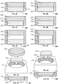
- FIGs. 2A-2F illustrate other example interior profiles for hollow frames 201-206.
- example frame 201 includes a 'step' feature 211 that serves to control the vertical arrangement of the light emitting chip 100 and the cap 230.
- the step 211 may be situated to control the extent to which the contacts of the light emitting chip 100 extend beyond the lower surface of the frame 201 when the cap 230 is inserted.
- frame 202 includes a sloped wall segment 212 that facilitates the insertion of the light emitting chip 100 into the frame 210, and also serves to re-direct any side emitted light from the cap 230 away from the light emitting chip 100.
- the sloped wall segment 212 extends to the lower surface of the frame 210.
- the cap 230' is created by dispensing a material in liquid or paste form into the cavity formed by the opening in the frame 210, then solidifying the material.
- the material may be silicone with optional wavelength conversion material that is applied in liquid form then cured to form a rigid cap 230'.
- the liquid or paste material may serve as the adhesive that attaches the chip 100 to the frame 210.
- frame 204 also includes a cap 230' that is dispensed into the cavity, but in this example, the walls 213 are not sloped.
- frame 205 includes an intermediate optical element 240 situated between the chip 100 and the cap 230.
- This optical element 240 may provide a particular optical effect, or it may enhance the light extraction efficiency by providing an index of refraction that is between the indices of refraction of the chip 100 and the cap 230.
- This optical element 240 is illustrated as a pre-formed parallelepiped, but it may be of any shape, and may be dispensed in liquid or paste form then solidified (not illustrated).
- the dispensed optical element 240 may serve to attach the chip 100 to the frame 210.
- One or more of the elements 230, 240, 100 may fit tightly inside frame 210.
- example frame 206 includes sloped wall segments 212, a pre-formed intermediate optical element 240, and a cap 230' that is dispensed in liquid or paste form and serves to attach the chip 100 and optical element 240 to the frame 210.
- the opening in the frame 210 is preferably shaped to correspond to the shape of the light emitting chip, which is typically rectilinear, to minimize the footprint of the resultant device 200 (or 201-206), other shaped openings may be provided. For example, because it is generally simpler to drill or bore circular holes through a material, cylindric or conic holes may be provided as illustrated in FIGs. 3A-3D .
- example device 301 includes frame 210 and a cylindrical hole in which a rectilinear light emitting chip 100 and a circular cap 230 are placed.
- the size of the hole is such that it circumscribes the light emitting chip 100 i.e. the diagonal of the light emitting chip 100 is less than or equal to the diameter of the cylindrical hole. In this manner, the extra footprint overhead caused by a cylindrical hole instead of a rectilinear hole is minimized.
- the light emitting chip 100 is pre-attached to the circular cap 230, then the pair of elements 100, 230 are placed within the cylindrical frame 210.
- the space between the chip 100 and the cylindrical walls 315 of the frame 210 may be filled with a reflective material, such as a dielectric paste that is subsequently hardened.
- the frame 210 includes a conic hole, with the size of the opening at the bottom surface of the frame 210 circumscribing the chip 100.
- the cap 230' is dispensed within the conic cavity in liquid or paste form, then hardened, and may serve to attach the chip 100 to the frame 210.
- the walls 325 may be reflective.
- each singulated module includes a plurality of light emitting chips.
- Multiple chip modules are commonly used for high power applications, such as automotive lighting modules.
- FIGs. 5A-5B illustrates example light emitting modules that includes a plurality of light emitting diodes within the light emitting module.
- the light emitting modules 501, 502 comprise one or more rows of four light emitting chips 100 with caps 230. That is, the modules 501, 502 may be a 'linear' light strip comprising four chips 100, or an 'MxN' array of chips 100.
- the variables M or N may be 4 or any other suitable integer.
- the placement of the chips 100 within defined cavities in the frame provides for a simple method of achieving the high alignment precision that may be required for certain automotive lamps.
- FIG. 5A illustrates a frame 510 in which each light emitting chip 100 is inserted first, followed by a corresponding cap 230.
- FIG. 5B illustrates the same frame 510 in which the cap 230 is inserted first, followed by the 'face-down' insertion of the light emitting chip 100.
- This method provides an advantage in that the caps 230 provide a level surface with the frame 510, as contrast to the protruding contacts of the light emitting chip 100. This may simplify the assembly process, and provide a wider range of options with regard to the choice of materials used as the removable sheet (280 in FIG. 1B ) that provides a surface upon which the first inserted element is supported during the assembly process. That is, the requirement that the sheet 280 be stretchable to accommodate the contacts 130, as illustrated in FIG. 1C , is eliminated.
- FIG. 6 illustrates an example alternative assembly method.
- the caps 230 are placed in a frame 610, and the light emitting chips 100 are attached to a substrate 650, such as a printed circuit board. After attaching the light emitting chips 100 to the substrate 650, the frame 610 with caps 230 is placed upon the substrate.
- FIG. 6 illustrates a multi-chip module 601
- single chip modules may be assembled in the same way.
- the figures illustrate a frame 210 that encloses all of the elements 100, 230, 240 it is possible to operate the invention in an embodiment wherein some or all of the cap 230 extends above the frame 210 and is shaped to provide a particular optical effect.
- the cap 230 may be mushroom-shaped, the upper portion providing a wider distribution of the emitted light.
- some or all of the optical element 240 may extend above the frame 210, and the cap 230 may encapsulate the portion of the optical element 240 extending beyond the frame 210.
- the cap 230 may also be omitted and the optical element 240 may be shaped to provide the aforementioned desired optical effect.
Claims (15)
- Dispositif d'émission de lumière comprenant :
au moins une puce d'émission de lumière (100) comprenant :
un substrat (110) sur lequel un élément d'émission de lumière (120) est situé, dans lequel :l'élément d'émission de lumière (120) comprend une région active qui est intercalée entre un semi-conducteur de type n et un semi-conducteur de type p, etla lumière émise à partir d'une première surface d'émission de lumière de l'élément d'émission de lumière (120) est émise à partir d'au moins une surface d'émission de lumière du substrat (110) ;des pastilles de contact (130) qui sont formées sur une deuxième surface de l'élément d'émission de lumière (120) qui est opposée à la première surface d'émission de lumière, dans lequel au moins une première pastille de contact est connectée au semi-conducteur de type n et une deuxième pastille de contact est connectée au semi-conducteur de type p ; etun cadre (210) agencé de manière à entourer le substrat (110) et l'élément d'émission de lumière (120) de sorte qu'au moins une partie des pastilles de contact (130) et au moins une partie du substrat (110) ne soient pas obstruées par le cadre (210),caractérisé en ce quela puce d'émission de lumière (100) est fixée dans le cadre (210) en ce que :- le cadre (210) est pliable et une ouverture dans le cadre (210) est dimensionnée pour réaliser un assemblage par frottement ;- les parois (215) sur le cadre (210) ou les parois latérales de la puce d'émission de lumière (100) sont revêtues d'un adhésif avant que la puce d'émission de lumière (100) soit insérée dans le cadre (210) ; ou- le cadre (210) est un matériau rétractable qui est rétracté après que la puce d'émission de lumière (100) a été insérée dans le cadre (210). - Dispositif selon la revendication 1, dans lequel le substrat (110) est un substrat de croissance sur lequel l'élément d'émission de lumière (120) est formé.
- Dispositif selon la revendication 1, dans lequel le substrat (110) comprend un substrat en saphir structuré.
- Dispositif selon la revendication 1, comprenant un couvercle (230) qui est entouré par le cadre (210), reçoit la lumière provenant du substrat (110), et émet la lumière à partir d'une surface d'émission de lumière du couvercle (230).
- Dispositif selon la revendication 4, dans lequel le couvercle (230) comprend un matériau de conversion de longueur d'onde qui absorbe une partie ou la totalité de la lumière provenant de l'élément d'émission de lumière (120) et qui la convertit en une lumière d'une longueur d'onde différente.
- Dispositif selon la revendication 4, dans lequel le cadre (210) comprend des parois intérieures réfléchissantes adjacentes au substrat (110) et au couvercle (230).
- Dispositif selon la revendication 1, dans lequel le cadre (210) entoure une pluralité d'éléments d'émission de lumière (120).
- Dispositif selon la revendication 7, comprenant en outre une structure de cadre comprenant :le cadre (210) qui comprend une pluralité d'ouvertures,une pluralité de puces d'émission de lumière (100) qui sont situées dans la pluralité d'ouvertures, chacune des puces d'émission de lumière (100) comprenant :un substrat sur lequel un élément d'émission de lumière est situé et à travers lequel la lumière provenant de l'élément d'émission de lumière est émise, etdes pastilles de contact qui sont formées sur une première surface de l'élément d'émission de lumière qui est opposée au substrat ;dans lequel chacune des ouvertures comprend des parois qui entourent la puce d'émission de lumière (100) dans l'ouverture et permettent un contact externe directement aux pastilles de contact (130) et permettent à la lumière provenant du substrat (110) de sortir de la structure de cadre.
- Dispositif selon la revendication 8, comprenant une pluralité de couvercles (230) qui sont situés dans la pluralité d'ouvertures, chaque couvercle (230) étant couplé optiquement au substrat (110) de la puce d'émission de lumière (100) dans au moins l'une des ouvertures.
- Dispositif selon la revendication 9, dans lequel chaque couvercle (230) comprend un matériau de conversion de longueur d'onde.
- Dispositif selon la revendication 10, dans lequel chaque couvercle (230) est un élément préformé qui est placé dans au moins l'une des ouvertures.
- Dispositif selon la revendication 11, dans lequel chaque ouverture comprend une caractéristique étagée (211) qui introduit une limitation dans l'ouverture, dans lequel la limitation est agencée pour contrôler un emplacement du couvercle (230) et de la puce d'émission de lumière (100) dans l'ouverture.
- Procédé de formation de dispositifs d'émission de lumière comprenant :la fourniture d'une structure de cadre qui comprend une pluralité d'ouvertures ;le placement d'une puce d'émission de lumière (100) dans chacune des ouvertures ;la fixation de la puce d'émission de lumière (100) dans le cadre (210) en ce que :- le cadre (210) est pliable et une ouverture dans le cadre (210) est dimensionnée pour réaliser un assemblage par frottement ;- les parois (215) sur le cadre (210) ou les parois latérales de la puce d'émission de lumière (100) sont revêtues d'un adhésif avant que la puce d'émission de lumière (100) soit insérée dans le cadre (210) ; ou- le cadre (210) est un matériau rétractable qui est rétracté après que la puce d'émission de lumière (100) a été insérée dans le cadre (210) ;chacune des puces d'émission de lumière (100) comprenant :un substrat (110) sur lequel un élément d'émission de lumière (120) est situé et à travers lequel la lumière provenant de l'élément d'émission de lumière (120) est émise, etdes pastilles de contact (130) qui sont formées sur une surface de l'élément d'émission de lumière (120) qui est opposée au substrat (110) ; etle tranchage de la structure de cadre pour obtenir des modules d'émission de lumière individuels qui comprennent un ou plusieurs dispositifs d'émission de lumière qui sont enfermés dans les parois de chaque ouverture qui entourent la puce d'émission de lumière (100) dans l'ouverture et permettent un contact externe directement avec les pastilles de contact (130) et permettent à la lumière provenant du substrat (110) de sortir de la structure de cadre.
- Procédé selon la revendication 13, dans lequel le substrat (110) est un substrat de croissance sur lequel chacun des éléments d'émission de lumière (120) est formé.
- Procédé selon la revendication 13, comprenant le placement d'un élément de conversion de longueur d'onde dans au moins l'une des ouvertures.
Applications Claiming Priority (3)
| Application Number | Priority Date | Filing Date | Title |
|---|---|---|---|
| US201361877434P | 2013-09-13 | 2013-09-13 | |
| US201461936360P | 2014-02-06 | 2014-02-06 | |
| PCT/IB2014/064106 WO2015036887A1 (fr) | 2013-09-13 | 2014-08-28 | Boîtier à grille de connexions pour del à puce retournée |
Publications (2)
| Publication Number | Publication Date |
|---|---|
| EP3044809A1 EP3044809A1 (fr) | 2016-07-20 |
| EP3044809B1 true EP3044809B1 (fr) | 2019-04-24 |
Family
ID=51743501
Family Applications (1)
| Application Number | Title | Priority Date | Filing Date |
|---|---|---|---|
| EP14786296.5A Active EP3044809B1 (fr) | 2013-09-13 | 2014-08-28 | Boîtier à grille de connexions pour del à puce retournée |
Country Status (6)
| Country | Link |
|---|---|
| US (2) | US9698323B2 (fr) |
| EP (1) | EP3044809B1 (fr) |
| JP (1) | JP6263628B2 (fr) |
| KR (1) | KR102264061B1 (fr) |
| CN (1) | CN105706237B (fr) |
| WO (1) | WO2015036887A1 (fr) |
Cited By (1)
| Publication number | Priority date | Publication date | Assignee | Title |
|---|---|---|---|---|
| EP4203082A4 (fr) * | 2020-10-22 | 2024-02-28 | Stanley Electric Co Ltd | Dispositif électroluminescent à semi-conducteur et module électroluminescent à semi-conducteur |
Families Citing this family (16)
| Publication number | Priority date | Publication date | Assignee | Title |
|---|---|---|---|---|
| CN105706237B (zh) * | 2013-09-13 | 2019-10-18 | 亮锐控股有限公司 | 用于倒装芯片led的基于框架的封装 |
| EP3093894B1 (fr) * | 2015-05-15 | 2020-08-05 | OSRAM GmbH | Procédé d'assemblage de dispositifs d'éclairage et dispositif correspondant |
| US10763404B2 (en) * | 2015-10-05 | 2020-09-01 | Maven Optronics Co., Ltd. | Light emitting device with beveled reflector and manufacturing method of the same |
| JP2017116372A (ja) * | 2015-12-24 | 2017-06-29 | 日東電工株式会社 | 蛍光体層付光半導体素子の検査方法 |
| KR20180100157A (ko) * | 2015-12-29 | 2018-09-07 | 루미리즈 홀딩 비.브이. | 측면 반사기들 및 인광체를 갖는 플립 칩 led |
| DE102016104202A1 (de) | 2016-03-08 | 2017-09-14 | Osram Opto Semiconductors Gmbh | Optoelektronisches Halbleiterbauteil |
| DE102016112293A1 (de) * | 2016-07-05 | 2018-01-11 | Osram Opto Semiconductors Gmbh | Verfahren zum herstellen eines optoelektronischen bauelements und optoelektronisches bauelement |
| DE102016115629A1 (de) | 2016-08-23 | 2018-03-01 | Osram Opto Semiconductors Gmbh | Verfahren zum herstellen eines optoelektronischen bauelements |
| WO2018036618A1 (fr) * | 2016-08-23 | 2018-03-01 | Osram Opto Semiconductors Gmbh | Procédé de fabrication d'une pluralité de dispositifs optoélectroniques et dispositif optoélectronique |
| DE102017103328A1 (de) * | 2017-02-17 | 2018-08-23 | Osram Opto Semiconductors Gmbh | Verfahren zum Herstellen einer Konversionsvorrichtung mit einem Konversionselement und einer Streumaterialbeschichtung |
| KR20190033979A (ko) * | 2017-09-22 | 2019-04-01 | 주식회사 루멘스 | 색 변환 전극부를 갖는 수직형 발광소자 |
| KR20190051205A (ko) * | 2017-11-06 | 2019-05-15 | 주식회사 루멘스 | 엘이디 패키지 |
| DE102017130574A1 (de) * | 2017-12-19 | 2019-06-19 | Osram Opto Semiconductors Gmbh | Verfahren zur Herstellung eines Konversionselements und Konversionselement |
| EP3543776A1 (fr) * | 2018-03-23 | 2019-09-25 | Maven Optronics Co., Ltd. | Dispositif électroluminescent linéaire de la taille d'une puce |
| DE102018121338A1 (de) * | 2018-08-31 | 2020-03-05 | Osram Opto Semiconductors Gmbh | Optoelektronische leuchtvorrichtung, optoelektronische beleuchtungseinrichtung und herstellungsverfahren |
| DE102022112418A1 (de) * | 2022-05-18 | 2023-11-23 | Ams-Osram International Gmbh | Optoelektronische vorrichtung und verfahren zur herstellung einer optoelektronischen vorrichtung |
Family Cites Families (33)
| Publication number | Priority date | Publication date | Assignee | Title |
|---|---|---|---|---|
| US5824186A (en) * | 1993-12-17 | 1998-10-20 | The Regents Of The University Of California | Method and apparatus for fabricating self-assembling microstructures |
| US6184544B1 (en) * | 1998-01-29 | 2001-02-06 | Rohm Co., Ltd. | Semiconductor light emitting device with light reflective current diffusion layer |
| DE10041328B4 (de) * | 2000-08-23 | 2018-04-05 | Osram Opto Semiconductors Gmbh | Verpackungseinheit für Halbleiterchips |
| JP4280050B2 (ja) * | 2002-10-07 | 2009-06-17 | シチズン電子株式会社 | 白色発光装置 |
| JP2004192720A (ja) * | 2002-12-11 | 2004-07-08 | Sankyo Seiki Mfg Co Ltd | 光ヘッド装置 |
| US7517728B2 (en) * | 2004-03-31 | 2009-04-14 | Cree, Inc. | Semiconductor light emitting devices including a luminescent conversion element |
| US7456499B2 (en) * | 2004-06-04 | 2008-11-25 | Cree, Inc. | Power light emitting die package with reflecting lens and the method of making the same |
| CN101138094B (zh) * | 2005-03-09 | 2010-10-13 | 旭化成电子材料元件株式会社 | 光学器件及光学器件的制造方法 |
| CN100394621C (zh) * | 2005-07-29 | 2008-06-11 | 东莞市福地电子材料有限公司 | 氮化镓基发光二极管芯片的制造方法 |
| WO2007147278A2 (fr) * | 2006-06-21 | 2007-12-27 | Gerhard Staufert | Source de lumière del et son procédé |
| US7791096B2 (en) * | 2007-06-08 | 2010-09-07 | Koninklijke Philips Electronics N.V. | Mount for a semiconductor light emitting device |
| US9024340B2 (en) * | 2007-11-29 | 2015-05-05 | Nichia Corporation | Light emitting apparatus and method for producing the same |
| US8454216B2 (en) * | 2008-09-05 | 2013-06-04 | Koninklijke Philips Electronics N.V. | Lamp assembly |
| US20100207140A1 (en) | 2009-02-19 | 2010-08-19 | Koninklijke Philips Electronics N.V. | Compact molded led module |
| JP5326705B2 (ja) * | 2009-03-17 | 2013-10-30 | 日亜化学工業株式会社 | 発光装置 |
| CN101587933B (zh) * | 2009-07-07 | 2010-12-08 | 苏州晶方半导体科技股份有限公司 | 发光二极管的晶圆级封装结构及其制造方法 |
| DE102009036621B4 (de) | 2009-08-07 | 2023-12-21 | OSRAM Opto Semiconductors Gesellschaft mit beschränkter Haftung | Optoelektronisches Halbleiterbauteil |
| KR101039881B1 (ko) * | 2009-12-21 | 2011-06-09 | 엘지이노텍 주식회사 | 발광소자 및 그를 이용한 라이트 유닛 |
| KR100986571B1 (ko) * | 2010-02-04 | 2010-10-07 | 엘지이노텍 주식회사 | 발광소자 패키지 및 그 제조방법 |
| DE102010025319B4 (de) | 2010-06-28 | 2022-05-25 | OSRAM Opto Semiconductors Gesellschaft mit beschränkter Haftung | Verfahren zur Herstellung eines oberflächenmontierbaren Halbleiterbauelements und oberflächenmontierbare Halbleiterbauelemente |
| US20120074434A1 (en) * | 2010-09-24 | 2012-03-29 | Jun Seok Park | Light emitting device package and lighting apparatus using the same |
| JP5745319B2 (ja) * | 2011-04-14 | 2015-07-08 | 日東電工株式会社 | 蛍光反射シート、および、発光ダイオード装置の製造方法 |
| JP5840377B2 (ja) * | 2011-04-14 | 2016-01-06 | 日東電工株式会社 | 反射樹脂シートおよび発光ダイオード装置の製造方法 |
| KR20130014256A (ko) * | 2011-07-29 | 2013-02-07 | 엘지이노텍 주식회사 | 발광 소자 패키지 및 이를 이용한 조명 시스템 |
| KR101219106B1 (ko) | 2011-08-01 | 2013-01-11 | 삼성전자주식회사 | 발광소자 패키지 및 그 제조방법 |
| WO2013056927A1 (fr) | 2011-10-20 | 2013-04-25 | Osram Gmbh | Pièce de recouvrement conçue pour un support d'un dispositif d'éclairage à semi-conducteurs |
| JP2013118210A (ja) * | 2011-12-01 | 2013-06-13 | Citizen Holdings Co Ltd | 半導体発光装置及びその製造方法 |
| EP2785570B1 (fr) * | 2011-12-02 | 2022-09-14 | Power Technology Holdings, LLC | Système et procédé d'optimisation de carburant dans un véhicule hybride |
| WO2013112435A1 (fr) * | 2012-01-24 | 2013-08-01 | Cooledge Lighting Inc. | Dispositifs électroluminescents présentant des puces distinctes à luminophore et procédés de fabrication associés |
| JP2014112669A (ja) * | 2012-11-12 | 2014-06-19 | Citizen Holdings Co Ltd | 半導体発光装置及びその製造方法 |
| CN105453277B (zh) * | 2013-07-30 | 2018-01-30 | 国立研究开发法人情报通信研究机构 | 半导体发光元件及其制造方法 |
| CN105706237B (zh) * | 2013-09-13 | 2019-10-18 | 亮锐控股有限公司 | 用于倒装芯片led的基于框架的封装 |
| US9343443B2 (en) * | 2014-02-05 | 2016-05-17 | Cooledge Lighting, Inc. | Light-emitting dies incorporating wavelength-conversion materials and related methods |
-
2014
- 2014-08-28 CN CN201480062353.2A patent/CN105706237B/zh active Active
- 2014-08-28 JP JP2016542405A patent/JP6263628B2/ja active Active
- 2014-08-28 US US14/917,217 patent/US9698323B2/en active Active
- 2014-08-28 KR KR1020167009653A patent/KR102264061B1/ko active IP Right Grant
- 2014-08-28 EP EP14786296.5A patent/EP3044809B1/fr active Active
- 2014-08-28 WO PCT/IB2014/064106 patent/WO2015036887A1/fr active Application Filing
-
2017
- 2017-07-01 US US15/640,482 patent/US20170301841A1/en not_active Abandoned
Non-Patent Citations (1)
| Title |
|---|
| None * |
Cited By (1)
| Publication number | Priority date | Publication date | Assignee | Title |
|---|---|---|---|---|
| EP4203082A4 (fr) * | 2020-10-22 | 2024-02-28 | Stanley Electric Co Ltd | Dispositif électroluminescent à semi-conducteur et module électroluminescent à semi-conducteur |
Also Published As
| Publication number | Publication date |
|---|---|
| JP6263628B2 (ja) | 2018-01-17 |
| EP3044809A1 (fr) | 2016-07-20 |
| CN105706237B (zh) | 2019-10-18 |
| US20160240755A1 (en) | 2016-08-18 |
| CN105706237A (zh) | 2016-06-22 |
| KR102264061B1 (ko) | 2021-06-14 |
| JP2016536804A (ja) | 2016-11-24 |
| KR20160055880A (ko) | 2016-05-18 |
| WO2015036887A1 (fr) | 2015-03-19 |
| US20170301841A1 (en) | 2017-10-19 |
| US9698323B2 (en) | 2017-07-04 |
Similar Documents
| Publication | Publication Date | Title |
|---|---|---|
| EP3044809B1 (fr) | Boîtier à grille de connexions pour del à puce retournée | |
| EP2666193B1 (fr) | Boîtier de del avec enrobage | |
| JP6203759B2 (ja) | Ledチップの製造方法 | |
| JP5503844B2 (ja) | 発光ダイオード素子 | |
| US6881980B1 (en) | Package structure of light emitting diode | |
| US9512968B2 (en) | LED module | |
| KR102146595B1 (ko) | 측면 방출을 위한 형상의 성장 기판을 가지는 led | |
| EP2745320B1 (fr) | Chambre de mélange de del munie de parois réfléchissantes formées dans des fentes | |
| JP2007287713A (ja) | 発光装置及びその製造方法 | |
| SG173518A1 (en) | Led leadframe package, led package using the same, and method of manufacturing the led package | |
| EP3022779B1 (fr) | Del de pc à élément optique et sans substrat de support | |
| KR20120072629A (ko) | 발광소자 패키지 및 그 제조방법 | |
| US9209373B2 (en) | High power plastic leaded chip carrier with integrated metal reflector cup and direct heat sink | |
| WO2013118076A1 (fr) | Dispositif électroluminescent encapsulé de coût réduit | |
| US20210367125A1 (en) | System and method of manufacture for led packages | |
| KR20120085085A (ko) | 칩 온 보드형 발광 모듈 및 상기 발광 모듈의 제조 방법 | |
| KR101461153B1 (ko) | 반도체 소자 구조물을 제조하는 방법 |
Legal Events
| Date | Code | Title | Description |
|---|---|---|---|
| PUAI | Public reference made under article 153(3) epc to a published international application that has entered the european phase |
Free format text: ORIGINAL CODE: 0009012 |
|
| 17P | Request for examination filed |
Effective date: 20160413 |
|
| AK | Designated contracting states |
Kind code of ref document: A1 Designated state(s): AL AT BE BG CH CY CZ DE DK EE ES FI FR GB GR HR HU IE IS IT LI LT LU LV MC MK MT NL NO PL PT RO RS SE SI SK SM TR |
|
| AX | Request for extension of the european patent |
Extension state: BA ME |
|
| DAX | Request for extension of the european patent (deleted) | ||
| STAA | Information on the status of an ep patent application or granted ep patent |
Free format text: STATUS: EXAMINATION IS IN PROGRESS |
|
| 17Q | First examination report despatched |
Effective date: 20180418 |
|
| RAP1 | Party data changed (applicant data changed or rights of an application transferred) |
Owner name: LUMILEDS HOLDING B.V. |
|
| RIC1 | Information provided on ipc code assigned before grant |
Ipc: H01L 25/075 20060101AFI20181030BHEP Ipc: H01L 33/58 20100101ALI20181030BHEP Ipc: H01L 33/48 20100101ALI20181030BHEP Ipc: H01L 33/50 20100101ALI20181030BHEP Ipc: H01L 33/60 20100101ALI20181030BHEP Ipc: H01L 33/62 20100101ALN20181030BHEP Ipc: H01L 33/00 20100101ALI20181030BHEP |
|
| GRAP | Despatch of communication of intention to grant a patent |
Free format text: ORIGINAL CODE: EPIDOSNIGR1 |
|
| STAA | Information on the status of an ep patent application or granted ep patent |
Free format text: STATUS: GRANT OF PATENT IS INTENDED |
|
| INTG | Intention to grant announced |
Effective date: 20181210 |
|
| RAP1 | Party data changed (applicant data changed or rights of an application transferred) |
Owner name: LUMILEDS HOLDING B.V. |
|
| GRAS | Grant fee paid |
Free format text: ORIGINAL CODE: EPIDOSNIGR3 |
|
| GRAA | (expected) grant |
Free format text: ORIGINAL CODE: 0009210 |
|
| STAA | Information on the status of an ep patent application or granted ep patent |
Free format text: STATUS: THE PATENT HAS BEEN GRANTED |
|
| AK | Designated contracting states |
Kind code of ref document: B1 Designated state(s): AL AT BE BG CH CY CZ DE DK EE ES FI FR GB GR HR HU IE IS IT LI LT LU LV MC MK MT NL NO PL PT RO RS SE SI SK SM TR |
|
| REG | Reference to a national code |
Ref country code: GB Ref legal event code: FG4D |
|
| REG | Reference to a national code |
Ref country code: CH Ref legal event code: EP |
|
| REG | Reference to a national code |
Ref country code: AT Ref legal event code: REF Ref document number: 1125153 Country of ref document: AT Kind code of ref document: T Effective date: 20190515 Ref country code: IE Ref legal event code: FG4D |
|
| REG | Reference to a national code |
Ref country code: DE Ref legal event code: R096 Ref document number: 602014045414 Country of ref document: DE |
|
| REG | Reference to a national code |
Ref country code: NL Ref legal event code: MP Effective date: 20190424 |
|
| REG | Reference to a national code |
Ref country code: LT Ref legal event code: MG4D |
|
| PG25 | Lapsed in a contracting state [announced via postgrant information from national office to epo] |
Ref country code: NL Free format text: LAPSE BECAUSE OF FAILURE TO SUBMIT A TRANSLATION OF THE DESCRIPTION OR TO PAY THE FEE WITHIN THE PRESCRIBED TIME-LIMIT Effective date: 20190424 |
|
| PG25 | Lapsed in a contracting state [announced via postgrant information from national office to epo] |
Ref country code: FI Free format text: LAPSE BECAUSE OF FAILURE TO SUBMIT A TRANSLATION OF THE DESCRIPTION OR TO PAY THE FEE WITHIN THE PRESCRIBED TIME-LIMIT Effective date: 20190424 Ref country code: HR Free format text: LAPSE BECAUSE OF FAILURE TO SUBMIT A TRANSLATION OF THE DESCRIPTION OR TO PAY THE FEE WITHIN THE PRESCRIBED TIME-LIMIT Effective date: 20190424 Ref country code: AL Free format text: LAPSE BECAUSE OF FAILURE TO SUBMIT A TRANSLATION OF THE DESCRIPTION OR TO PAY THE FEE WITHIN THE PRESCRIBED TIME-LIMIT Effective date: 20190424 Ref country code: NO Free format text: LAPSE BECAUSE OF FAILURE TO SUBMIT A TRANSLATION OF THE DESCRIPTION OR TO PAY THE FEE WITHIN THE PRESCRIBED TIME-LIMIT Effective date: 20190724 Ref country code: PT Free format text: LAPSE BECAUSE OF FAILURE TO SUBMIT A TRANSLATION OF THE DESCRIPTION OR TO PAY THE FEE WITHIN THE PRESCRIBED TIME-LIMIT Effective date: 20190824 Ref country code: SE Free format text: LAPSE BECAUSE OF FAILURE TO SUBMIT A TRANSLATION OF THE DESCRIPTION OR TO PAY THE FEE WITHIN THE PRESCRIBED TIME-LIMIT Effective date: 20190424 Ref country code: ES Free format text: LAPSE BECAUSE OF FAILURE TO SUBMIT A TRANSLATION OF THE DESCRIPTION OR TO PAY THE FEE WITHIN THE PRESCRIBED TIME-LIMIT Effective date: 20190424 Ref country code: LT Free format text: LAPSE BECAUSE OF FAILURE TO SUBMIT A TRANSLATION OF THE DESCRIPTION OR TO PAY THE FEE WITHIN THE PRESCRIBED TIME-LIMIT Effective date: 20190424 |
|
| PG25 | Lapsed in a contracting state [announced via postgrant information from national office to epo] |
Ref country code: BG Free format text: LAPSE BECAUSE OF FAILURE TO SUBMIT A TRANSLATION OF THE DESCRIPTION OR TO PAY THE FEE WITHIN THE PRESCRIBED TIME-LIMIT Effective date: 20190724 Ref country code: RS Free format text: LAPSE BECAUSE OF FAILURE TO SUBMIT A TRANSLATION OF THE DESCRIPTION OR TO PAY THE FEE WITHIN THE PRESCRIBED TIME-LIMIT Effective date: 20190424 Ref country code: LV Free format text: LAPSE BECAUSE OF FAILURE TO SUBMIT A TRANSLATION OF THE DESCRIPTION OR TO PAY THE FEE WITHIN THE PRESCRIBED TIME-LIMIT Effective date: 20190424 Ref country code: GR Free format text: LAPSE BECAUSE OF FAILURE TO SUBMIT A TRANSLATION OF THE DESCRIPTION OR TO PAY THE FEE WITHIN THE PRESCRIBED TIME-LIMIT Effective date: 20190725 Ref country code: PL Free format text: LAPSE BECAUSE OF FAILURE TO SUBMIT A TRANSLATION OF THE DESCRIPTION OR TO PAY THE FEE WITHIN THE PRESCRIBED TIME-LIMIT Effective date: 20190424 |
|
| REG | Reference to a national code |
Ref country code: AT Ref legal event code: MK05 Ref document number: 1125153 Country of ref document: AT Kind code of ref document: T Effective date: 20190424 |
|
| PG25 | Lapsed in a contracting state [announced via postgrant information from national office to epo] |
Ref country code: IS Free format text: LAPSE BECAUSE OF FAILURE TO SUBMIT A TRANSLATION OF THE DESCRIPTION OR TO PAY THE FEE WITHIN THE PRESCRIBED TIME-LIMIT Effective date: 20190824 |
|
| REG | Reference to a national code |
Ref country code: DE Ref legal event code: R097 Ref document number: 602014045414 Country of ref document: DE |
|
| PG25 | Lapsed in a contracting state [announced via postgrant information from national office to epo] |
Ref country code: RO Free format text: LAPSE BECAUSE OF FAILURE TO SUBMIT A TRANSLATION OF THE DESCRIPTION OR TO PAY THE FEE WITHIN THE PRESCRIBED TIME-LIMIT Effective date: 20190424 Ref country code: SK Free format text: LAPSE BECAUSE OF FAILURE TO SUBMIT A TRANSLATION OF THE DESCRIPTION OR TO PAY THE FEE WITHIN THE PRESCRIBED TIME-LIMIT Effective date: 20190424 Ref country code: CZ Free format text: LAPSE BECAUSE OF FAILURE TO SUBMIT A TRANSLATION OF THE DESCRIPTION OR TO PAY THE FEE WITHIN THE PRESCRIBED TIME-LIMIT Effective date: 20190424 Ref country code: EE Free format text: LAPSE BECAUSE OF FAILURE TO SUBMIT A TRANSLATION OF THE DESCRIPTION OR TO PAY THE FEE WITHIN THE PRESCRIBED TIME-LIMIT Effective date: 20190424 Ref country code: DK Free format text: LAPSE BECAUSE OF FAILURE TO SUBMIT A TRANSLATION OF THE DESCRIPTION OR TO PAY THE FEE WITHIN THE PRESCRIBED TIME-LIMIT Effective date: 20190424 Ref country code: AT Free format text: LAPSE BECAUSE OF FAILURE TO SUBMIT A TRANSLATION OF THE DESCRIPTION OR TO PAY THE FEE WITHIN THE PRESCRIBED TIME-LIMIT Effective date: 20190424 |
|
| PG25 | Lapsed in a contracting state [announced via postgrant information from national office to epo] |
Ref country code: IT Free format text: LAPSE BECAUSE OF FAILURE TO SUBMIT A TRANSLATION OF THE DESCRIPTION OR TO PAY THE FEE WITHIN THE PRESCRIBED TIME-LIMIT Effective date: 20190424 Ref country code: SM Free format text: LAPSE BECAUSE OF FAILURE TO SUBMIT A TRANSLATION OF THE DESCRIPTION OR TO PAY THE FEE WITHIN THE PRESCRIBED TIME-LIMIT Effective date: 20190424 |
|
| PLBE | No opposition filed within time limit |
Free format text: ORIGINAL CODE: 0009261 |
|
| STAA | Information on the status of an ep patent application or granted ep patent |
Free format text: STATUS: NO OPPOSITION FILED WITHIN TIME LIMIT |
|
| PG25 | Lapsed in a contracting state [announced via postgrant information from national office to epo] |
Ref country code: TR Free format text: LAPSE BECAUSE OF FAILURE TO SUBMIT A TRANSLATION OF THE DESCRIPTION OR TO PAY THE FEE WITHIN THE PRESCRIBED TIME-LIMIT Effective date: 20190424 |
|
| 26N | No opposition filed |
Effective date: 20200127 |
|
| PG25 | Lapsed in a contracting state [announced via postgrant information from national office to epo] |
Ref country code: CH Free format text: LAPSE BECAUSE OF NON-PAYMENT OF DUE FEES Effective date: 20190831 Ref country code: SI Free format text: LAPSE BECAUSE OF FAILURE TO SUBMIT A TRANSLATION OF THE DESCRIPTION OR TO PAY THE FEE WITHIN THE PRESCRIBED TIME-LIMIT Effective date: 20190424 Ref country code: LI Free format text: LAPSE BECAUSE OF NON-PAYMENT OF DUE FEES Effective date: 20190831 Ref country code: LU Free format text: LAPSE BECAUSE OF NON-PAYMENT OF DUE FEES Effective date: 20190828 Ref country code: MC Free format text: LAPSE BECAUSE OF FAILURE TO SUBMIT A TRANSLATION OF THE DESCRIPTION OR TO PAY THE FEE WITHIN THE PRESCRIBED TIME-LIMIT Effective date: 20190424 |
|
| REG | Reference to a national code |
Ref country code: BE Ref legal event code: MM Effective date: 20190831 |
|
| PG25 | Lapsed in a contracting state [announced via postgrant information from national office to epo] |
Ref country code: IE Free format text: LAPSE BECAUSE OF NON-PAYMENT OF DUE FEES Effective date: 20190828 |
|
| PG25 | Lapsed in a contracting state [announced via postgrant information from national office to epo] |
Ref country code: BE Free format text: LAPSE BECAUSE OF NON-PAYMENT OF DUE FEES Effective date: 20190831 |
|
| PG25 | Lapsed in a contracting state [announced via postgrant information from national office to epo] |
Ref country code: CY Free format text: LAPSE BECAUSE OF FAILURE TO SUBMIT A TRANSLATION OF THE DESCRIPTION OR TO PAY THE FEE WITHIN THE PRESCRIBED TIME-LIMIT Effective date: 20190424 |
|
| PG25 | Lapsed in a contracting state [announced via postgrant information from national office to epo] |
Ref country code: HU Free format text: LAPSE BECAUSE OF FAILURE TO SUBMIT A TRANSLATION OF THE DESCRIPTION OR TO PAY THE FEE WITHIN THE PRESCRIBED TIME-LIMIT; INVALID AB INITIO Effective date: 20140828 Ref country code: MT Free format text: LAPSE BECAUSE OF FAILURE TO SUBMIT A TRANSLATION OF THE DESCRIPTION OR TO PAY THE FEE WITHIN THE PRESCRIBED TIME-LIMIT Effective date: 20190424 |
|
| PG25 | Lapsed in a contracting state [announced via postgrant information from national office to epo] |
Ref country code: MK Free format text: LAPSE BECAUSE OF FAILURE TO SUBMIT A TRANSLATION OF THE DESCRIPTION OR TO PAY THE FEE WITHIN THE PRESCRIBED TIME-LIMIT Effective date: 20190424 |
|
| P01 | Opt-out of the competence of the unified patent court (upc) registered |
Effective date: 20230530 |
|
| PGFP | Annual fee paid to national office [announced via postgrant information from national office to epo] |
Ref country code: GB Payment date: 20230822 Year of fee payment: 10 |
|
| PGFP | Annual fee paid to national office [announced via postgrant information from national office to epo] |
Ref country code: FR Payment date: 20230824 Year of fee payment: 10 Ref country code: DE Payment date: 20230828 Year of fee payment: 10 |