EP3016129B1 - X-ray generating tube, x-ray generating apparatus, and radiography system - Google Patents
X-ray generating tube, x-ray generating apparatus, and radiography system Download PDFInfo
- Publication number
- EP3016129B1 EP3016129B1 EP15190789.6A EP15190789A EP3016129B1 EP 3016129 B1 EP3016129 B1 EP 3016129B1 EP 15190789 A EP15190789 A EP 15190789A EP 3016129 B1 EP3016129 B1 EP 3016129B1
- Authority
- EP
- European Patent Office
- Prior art keywords
- conductive film
- tube
- ray generating
- insulating tube
- ray
- Prior art date
- Legal status (The legal status is an assumption and is not a legal conclusion. Google has not performed a legal analysis and makes no representation as to the accuracy of the status listed.)
- Active
Links
- 238000002601 radiography Methods 0.000 title claims description 13
- 238000005304 joining Methods 0.000 claims description 26
- 238000010894 electron beam technology Methods 0.000 claims description 18
- 239000000463 material Substances 0.000 description 19
- 229910052751 metal Inorganic materials 0.000 description 16
- 239000002184 metal Substances 0.000 description 16
- 238000005219 brazing Methods 0.000 description 15
- 238000000034 method Methods 0.000 description 11
- 239000000945 filler Substances 0.000 description 10
- 238000010438 heat treatment Methods 0.000 description 6
- 229910000833 kovar Inorganic materials 0.000 description 6
- WFKWXMTUELFFGS-UHFFFAOYSA-N tungsten Chemical compound [W] WFKWXMTUELFFGS-UHFFFAOYSA-N 0.000 description 6
- 229910052721 tungsten Inorganic materials 0.000 description 6
- 239000010937 tungsten Substances 0.000 description 6
- BQCADISMDOOEFD-UHFFFAOYSA-N Silver Chemical compound [Ag] BQCADISMDOOEFD-UHFFFAOYSA-N 0.000 description 5
- 238000010586 diagram Methods 0.000 description 5
- 229910052709 silver Inorganic materials 0.000 description 5
- 239000004332 silver Substances 0.000 description 5
- ZOKXTWBITQBERF-UHFFFAOYSA-N Molybdenum Chemical compound [Mo] ZOKXTWBITQBERF-UHFFFAOYSA-N 0.000 description 4
- PXHVJJICTQNCMI-UHFFFAOYSA-N Nickel Chemical compound [Ni] PXHVJJICTQNCMI-UHFFFAOYSA-N 0.000 description 4
- 229910004353 Ti-Cu Inorganic materials 0.000 description 4
- 238000009826 distribution Methods 0.000 description 4
- 230000005684 electric field Effects 0.000 description 4
- 239000007788 liquid Substances 0.000 description 4
- 229910052750 molybdenum Inorganic materials 0.000 description 4
- 239000011733 molybdenum Substances 0.000 description 4
- 239000010936 titanium Substances 0.000 description 4
- PNEYBMLMFCGWSK-UHFFFAOYSA-N aluminium oxide Inorganic materials [O-2].[O-2].[O-2].[Al+3].[Al+3] PNEYBMLMFCGWSK-UHFFFAOYSA-N 0.000 description 3
- 229910010293 ceramic material Inorganic materials 0.000 description 3
- 238000010292 electrical insulation Methods 0.000 description 3
- 239000011521 glass Substances 0.000 description 3
- 239000007769 metal material Substances 0.000 description 3
- 238000012545 processing Methods 0.000 description 3
- 229910001369 Brass Inorganic materials 0.000 description 2
- RYGMFSIKBFXOCR-UHFFFAOYSA-N Copper Chemical compound [Cu] RYGMFSIKBFXOCR-UHFFFAOYSA-N 0.000 description 2
- XEEYBQQBJWHFJM-UHFFFAOYSA-N Iron Chemical compound [Fe] XEEYBQQBJWHFJM-UHFFFAOYSA-N 0.000 description 2
- 229910000792 Monel Inorganic materials 0.000 description 2
- RTAQQCXQSZGOHL-UHFFFAOYSA-N Titanium Chemical compound [Ti] RTAQQCXQSZGOHL-UHFFFAOYSA-N 0.000 description 2
- HCHKCACWOHOZIP-UHFFFAOYSA-N Zinc Chemical compound [Zn] HCHKCACWOHOZIP-UHFFFAOYSA-N 0.000 description 2
- 229910052782 aluminium Inorganic materials 0.000 description 2
- XAGFODPZIPBFFR-UHFFFAOYSA-N aluminium Chemical compound [Al] XAGFODPZIPBFFR-UHFFFAOYSA-N 0.000 description 2
- 239000010951 brass Substances 0.000 description 2
- 239000010949 copper Substances 0.000 description 2
- 229910052802 copper Inorganic materials 0.000 description 2
- 230000000694 effects Effects 0.000 description 2
- 238000011156 evaluation Methods 0.000 description 2
- 230000002349 favourable effect Effects 0.000 description 2
- 229910001385 heavy metal Inorganic materials 0.000 description 2
- 239000011810 insulating material Substances 0.000 description 2
- 230000001678 irradiating effect Effects 0.000 description 2
- 150000002739 metals Chemical class 0.000 description 2
- 229910052759 nickel Inorganic materials 0.000 description 2
- 238000009659 non-destructive testing Methods 0.000 description 2
- 239000003921 oil Substances 0.000 description 2
- 229910001220 stainless steel Inorganic materials 0.000 description 2
- 239000010935 stainless steel Substances 0.000 description 2
- 239000000758 substrate Substances 0.000 description 2
- 229910052715 tantalum Inorganic materials 0.000 description 2
- GUVRBAGPIYLISA-UHFFFAOYSA-N tantalum atom Chemical compound [Ta] GUVRBAGPIYLISA-UHFFFAOYSA-N 0.000 description 2
- 229910052719 titanium Inorganic materials 0.000 description 2
- 229910052725 zinc Inorganic materials 0.000 description 2
- 239000011701 zinc Substances 0.000 description 2
- 229910002708 Au–Cu Inorganic materials 0.000 description 1
- OKTJSMMVPCPJKN-UHFFFAOYSA-N Carbon Chemical compound [C] OKTJSMMVPCPJKN-UHFFFAOYSA-N 0.000 description 1
- VYZAMTAEIAYCRO-UHFFFAOYSA-N Chromium Chemical compound [Cr] VYZAMTAEIAYCRO-UHFFFAOYSA-N 0.000 description 1
- 229910001111 Fine metal Inorganic materials 0.000 description 1
- FYYHWMGAXLPEAU-UHFFFAOYSA-N Magnesium Chemical compound [Mg] FYYHWMGAXLPEAU-UHFFFAOYSA-N 0.000 description 1
- ATJFFYVFTNAWJD-UHFFFAOYSA-N Tin Chemical compound [Sn] ATJFFYVFTNAWJD-UHFFFAOYSA-N 0.000 description 1
- 238000009825 accumulation Methods 0.000 description 1
- 239000011230 binding agent Substances 0.000 description 1
- 239000002041 carbon nanotube Substances 0.000 description 1
- 229910021393 carbon nanotube Inorganic materials 0.000 description 1
- 239000000919 ceramic Substances 0.000 description 1
- 239000011651 chromium Substances 0.000 description 1
- 229910052804 chromium Inorganic materials 0.000 description 1
- 230000000052 comparative effect Effects 0.000 description 1
- 239000012141 concentrate Substances 0.000 description 1
- 239000000470 constituent Substances 0.000 description 1
- 239000002826 coolant Substances 0.000 description 1
- 238000000151 deposition Methods 0.000 description 1
- 238000003745 diagnosis Methods 0.000 description 1
- 238000001035 drying Methods 0.000 description 1
- 238000005516 engineering process Methods 0.000 description 1
- PCHJSUWPFVWCPO-UHFFFAOYSA-N gold Chemical compound [Au] PCHJSUWPFVWCPO-UHFFFAOYSA-N 0.000 description 1
- 229910052737 gold Inorganic materials 0.000 description 1
- 239000010931 gold Substances 0.000 description 1
- 238000003384 imaging method Methods 0.000 description 1
- 229910052742 iron Inorganic materials 0.000 description 1
- 229910052749 magnesium Inorganic materials 0.000 description 1
- 239000011777 magnesium Substances 0.000 description 1
- WPBNNNQJVZRUHP-UHFFFAOYSA-L manganese(2+);methyl n-[[2-(methoxycarbonylcarbamothioylamino)phenyl]carbamothioyl]carbamate;n-[2-(sulfidocarbothioylamino)ethyl]carbamodithioate Chemical compound [Mn+2].[S-]C(=S)NCCNC([S-])=S.COC(=O)NC(=S)NC1=CC=CC=C1NC(=S)NC(=O)OC WPBNNNQJVZRUHP-UHFFFAOYSA-L 0.000 description 1
- 238000004519 manufacturing process Methods 0.000 description 1
- 238000005259 measurement Methods 0.000 description 1
- 229910044991 metal oxide Inorganic materials 0.000 description 1
- 150000004706 metal oxides Chemical class 0.000 description 1
- 239000002923 metal particle Substances 0.000 description 1
- 238000001465 metallisation Methods 0.000 description 1
- 239000002480 mineral oil Substances 0.000 description 1
- 235000010446 mineral oil Nutrition 0.000 description 1
- 239000000203 mixture Substances 0.000 description 1
- 238000012986 modification Methods 0.000 description 1
- 230000004048 modification Effects 0.000 description 1
- 239000003960 organic solvent Substances 0.000 description 1
- 230000007170 pathology Effects 0.000 description 1
- -1 perfluoro Chemical group 0.000 description 1
- 230000002093 peripheral effect Effects 0.000 description 1
- 239000000843 powder Substances 0.000 description 1
- 238000007639 printing Methods 0.000 description 1
- 238000007789 sealing Methods 0.000 description 1
- 229920002545 silicone oil Polymers 0.000 description 1
- 239000007787 solid Substances 0.000 description 1
- 238000004544 sputter deposition Methods 0.000 description 1
- 239000000126 substance Substances 0.000 description 1
- 229910052718 tin Inorganic materials 0.000 description 1
- 239000011135 tin Substances 0.000 description 1
- 238000007740 vapor deposition Methods 0.000 description 1
Images

Classifications
-
- H—ELECTRICITY
- H01—ELECTRIC ELEMENTS
- H01J—ELECTRIC DISCHARGE TUBES OR DISCHARGE LAMPS
- H01J35/00—X-ray tubes
- H01J35/02—Details
- H01J35/16—Vessels; Containers; Shields associated therewith
-
- H—ELECTRICITY
- H01—ELECTRIC ELEMENTS
- H01J—ELECTRIC DISCHARGE TUBES OR DISCHARGE LAMPS
- H01J35/00—X-ray tubes
- H01J35/24—Tubes wherein the point of impact of the cathode ray on the anode or anticathode is movable relative to the surface thereof
-
- H—ELECTRICITY
- H01—ELECTRIC ELEMENTS
- H01J—ELECTRIC DISCHARGE TUBES OR DISCHARGE LAMPS
- H01J2235/00—X-ray tubes
- H01J2235/02—Electrical arrangements
-
- H—ELECTRICITY
- H01—ELECTRIC ELEMENTS
- H01J—ELECTRIC DISCHARGE TUBES OR DISCHARGE LAMPS
- H01J35/00—X-ray tubes
- H01J35/02—Details
- H01J35/04—Electrodes ; Mutual position thereof; Constructional adaptations therefor
- H01J35/08—Anodes; Anti cathodes
- H01J35/112—Non-rotating anodes
- H01J35/116—Transmissive anodes
Definitions
- the present invention relates to an X-ray generating tube generating an X-ray applicable to, for example, medical equipment and non-destructive testing apparatus, and an X-ray generating apparatus and a radiography system that use the X-ray generating tube.
- X-ray generating tubes generate an X-ray by applying high voltage in a vacuum container, thus causing an electron source to emit an electron beam and creating a collision between electrons and a target made of a metal material that has a high atomic number, such as tungsten.
- the voltage applied between a cathode, which includes the electron source, and an anode, which includes the target, is generally about 10 kV to about 150 kV, although varying depending on the use of the generated X-ray.
- the trunk of the vacuum container is built from an insulating tube that is made of an insulating material such as glass or a ceramic material in order to keep the interior under vacuum and to electrically insulate the cathode and the anode from each other.
- the location and amount of charge on the inner surface of the insulating tube vary depending on the distribution of points irradiated with the scattered electrons and secondary electrons, and the resultant difference in electric potential on the inner surface of the insulating tube may lead to a discharge that damages the insulating tube.
- connection between a low conductivity film and the electrodes in Japanese Patent Application Laid-Open No. S58-44662 . Accordingly, poor connection between the low conductivity film and the electrodes hinders the scattered electrons and the secondary electrons from freeing, thereby putting the conductive film itself into a charged state. The charged conductive film may disrupt the electron beam trajectory and change the X-ray output.
- an X-ray generating tube including: an anode including: a target generating an X-ray upon an irradiation with an electron beam; and an anode member which is electrically connected to the target and which holds the target; a cathode including: an electron emitting source having an electron emitting portion configured to irradiate an electron beam to the target; and a cathode member electrically connected to the electron emitting source; and an insulating tube having a pair of ends in a tube axis direction, one end of which is connected to the anode member and the other end of which is connected to the cathode member so that the target and the electron emitting portion face each other, in which the anode further includes an inner circumferential conductive film, which is positioned on an inner surface of the insulating tube at a distance from the cathode, and an end surface conductive film formed on the one end of the
- an X-ray generating apparatus including: the X-ray generating tube of the first embodiment of the present invention; and a drive circuit configured to apply a tube voltage between the anode and the cathode.
- a radiography system including: the X-ray generating apparatus of the second embodiment of the present invention; an X-ray detector configured to detect an X-ray that has been generated from the X-ray generating apparatus and transmitted through a subject; and a system control unit configured to control the X-ray generating apparatus and the X-ray detector in an integrated manner.
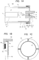
- FIG. 1A is an illustration of the schematic structure of a transmissive X-ray generating tube 102, which includes an electron emitting source 3 and a target 9.
- a member which has airtightness for maintaining vacuum and which is solid enough to withstand atmospheric pressure is preferred for an envelope 111 of the X-ray generating tube 102.
- the envelope 111 of this embodiment includes an insulating tube 110, a cathode 51, which includes the electron emitting source 3 such as an electron gun, and an anode 52, which includes the target 9 held by a target holding portion 43a and an anode member 43.
- the cathode 51 and the anode 52 form a part of the envelope 111, with the anode member 43 joined to the insulating tube 110 at one end and a cathode member 41 joined to the insulating tube 110 at the other end.
- the target 9 has as a component a transmissive substrate 21 serving as a transmissive window through which an X-ray beam 11 generated by irradiating a target layer 22 with an electron beam is taken out of the X-ray generating tube 102, and which also forms a part of the envelope 111.
- the cathode member 41 and the anode member 43, which are joined to the insulating tube 110 to be made of a metal material that has a linear expansion coefficient close to that of the insulating tube 110.
- Kovar trademarked in the U.S. to CRS Holdings, Inc.
- Monel trademarked in the U.S. to Special Metals Corporation
- the X-ray generating tube 102 generates the X-ray beam 11 by irradiating the target layer 22 of the target 9 with an electron beam 5, which is emitted from an electron emitting portion 2 included in the electron emitting source 3.
- a region 11a of the target layer 22 in which the X-ray is generated is called a focal spot of the X-ray beam 11.
- the target layer 22 is formed on the electron emitting source 3 side of the transmissive substrate 21 through which the X-ray is transmitted.
- the electron emitting portion 2 of the electron emitting source 3 is opposed to the target layer 22.
- tungsten, tantalum, or molybdenum is used for the target layer 22.
- the anode 52 of this embodiment includes the target 9, which generates an X-ray upon an irradiation with an electron beam, the target holding portion 43a, and the anode member 43, which defines the anode potential of the target 9.
- the anode member 43 includes the target holding portion 43a configured to hold the target 9, and an outer circumferential tubular portion 43b, which is provided in order to secure areal dimensions for joining the anode member 43 to the insulating tube 110.
- Metal such as Kovar, tungsten, molybdenum, or stainless steel is selected for the anode member 43, the outer circumferential tubular portion 43b, and the target holding portion 43a, which are included in the anode 52.
- Kovar, Monel, or the like is selected to give those components a linear expansion coefficient matching that of the insulating tube 110.
- the outer circumferential tubular portion 43b is shaped like a sleeve that extends from the target holding portion 43a toward the cathode 51.
- the outer circumferential tubular portion 43b defines the anode potential of a cathode-side part of the anode 52.
- the distance from the target holding portion 43a to an end of the outer circumferential tubular portion 43b on the cathode 51 side is preferred to be constant in the circumferential direction from the viewpoint of in-plane symmetry of the anode-side electric potential distribution.
- the in-plane symmetry of the electric potential distribution means that the electric potential distribution in a plane parallel to the anode member 42 is continuous in a tube circumference direction, without finding a region that is locally high in electric field in the tube circumference direction.
- the target holding portion 43a is joined to the target 9 to hold the target 9.
- the target holding portion 43a has a through-hole 42, and the opening of the through-hole 42 is closed to hold the target 9 at a point along the length of the through-hole 42.
- At least a part of the target holding portion 43a that extends outward from the target 9 to the outside of the envelope 111 is made of heavy metal such as tungsten or tantalum, or a material containing heavy metal, thereby enabling the target holding portion 43a to function as a collimator for controlling the emission angle of the X-ray beam 11.
- the target holding portion 43a and the outer circumferential tubular portion 43b may be formed as a seamless unitary member, or may be formed separately and subsequently joined together to form a unitary member.
- the electron emitting source 3 is configured to irradiate the target 9 with an electron beam that is emitted from the electron beam emitting portion 2.
- a hot cathode such as a tungsten filament or an impregnated cathode, or a cold cathode such as a carbon nanotube can be used for the electron emitting source 3.
- the electron emitting source 3 may include a grid electrode (not shown) and an electrostatic lens (not shown) for the purpose of controlling the beam diameter of the electron beam 5, the electron current density, on/off timing, and the like.
- Electrons contained in the electron beam 5 are accelerated to an energy level necessary to generate an X-ray in the target layer 22 by an accelerating electric field formed in an internal space 13 of the X-ray generating tube 102 which is sandwiched between the cathode 51 and the anode 52.
- the internal space 13 of the X-ray generating tube 102 is vacuum in order to secure a mean free path for the electron beam 5.
- the degree of vacuum of the internal space 13 is preferably 10 -8 Pa or more and 10 -4 Pa or less, more preferably from the viewpoint of the lifetime of the electron emitting source 3, 10 -8 Pa or more and 10 -6 Pa or less.
- the internal space 13 of the X-ray generating tube 102 is put under vacuum by exhausting the internal space 13 with the use of an exhaust pipe (not shown) and a vacuum pump (not shown), and then sealing the exhaust pipe.
- a getter may be formed in the internal space 13 of the X-ray generating tube 102 for the purpose of maintaining the vacuum.
- the X-ray generating tube 102 has as its trunk the insulating tube 110 in order to electrically insulate the electron emitting source 3, which is set to the cathode potential, and the target layer 22, which is set to the anode potential, from each other.
- the insulating tube 110 is made of an insulating material such as a glass material or a ceramic material.
- the insulating tube 110 may have a function of defining the gap between the electron beam emitting portion 2 and the target layer 22.
- an inner circumferential conductive film 112 is formed on the inner circumferential surface of the insulating tube 110 at a distance from the cathode 51.
- the inner circumferential conductive film 112 is connected to the anode member 43 via an end surface conductive film 113, which extends from an edge of the inner circumferential conductive film 112 on the target holding portion 43a side onto an end surface of the insulating tube 110 on the target holding portion 43a side.
- the end surface conductive film 113 is sandwiched between the end surface of the insulating tube 110 on the target holding portion 43a side and the target holding portion 43a to be electrically connected to the anode member 43.
- the inner circumferential conductive film 112 an outer circumferential conductive film 114, and the end surface conductive film 113 are included in the anode 52.
- the inner circumferential conductive film 112 can be, for example, a film of metal such as silver, copper, tin, gold, zinc, titanium, molybdenum, manganese, chromium, aluminum, or magnesium, a conductive film that contains one of those metals, or a metal oxide film.
- the material of the inner circumferential conductive film 112 is selected by taking into consideration the adhesion to the inner surface of the insulating tube 110.
- the inner circumferential conductive film 112 can be formed by a method in which a paste that is a mixture of a conductive substance with an organic solvent, a binder, and the like is prepared and applied, an arbitrary deposition method such as vapor deposition or sputtering, or other methods.
- a film preferred as the inner circumferential conductive film 112 has a thickness of from 100 nm to 500 ⁇ m, has sufficient conductivity, and is continuous in the tube circumference direction and a tube length direction so that the inner surface of the insulating tube 110 is not exposed within the extent of the inner circumferential conductive film 112.
- the preferred inner circumferential conductive film 112 is formed so as to stretch from the end of the insulating tube 110 on the target holding portion 43a side to a middle portion of the insulating tube 110 in the length direction as illustrated in FIG. 1A .
- an edge of the inner circumferential conductive film 112 on the cathode member 41 side in particular, to be positioned at a point which overlaps with the electron emitting source 3 and which is on the target holding portion 43a side beyond the midpoint of the insulating tube 110 in a tube axis direction. This is for covering the inner surface of the insulating tube 110 which is likely to be subjected to reflected electrons, thus preventing reflected electrons from charging the insulating tube 110 and from causing discharge as a result, and maintaining the withstand voltage between the cathode 51 and the anode 52.
- the preferred inner circumferential conductive film 112 is formed continuously in the tube circumference direction and length direction of the insulating tube 110 so that the charging of a region where the inner circumferential conductive film 112 is formed is prevented evenly.
- the end surface conductive film 113 can be formed from the same material, by the same method, and to the same thickness as the inner circumferential conductive film 112, and is formed so as to be continuous from the inner circumferential conductive film 112. In order to simplify the process and to facilitate the forming of a film that is continuous from the inner circumferential conductive film 112, it is preferred to form the end surface conductive film 113 at the same time as the inner circumferential conductive film 112.
- the preferred end surface conductive film 113 is formed on a part of the end surface of the insulating tube 110 on the anode member 43 side in the tube circumference direction. For example, it is preferred to arrange a plurality of end surface conductive films 113 each having a width of from 100 ⁇ m to 5 mm discretely in two to ten places on the end surface of the insulating tube 110 as illustrated in FIG. 1C . Forming the end surface conductive film 113 only in selective places on the end surface of the insulating tube 110 is accomplished by a method in which a paste material is applied directly in places, a pattern printing method, a method in which a film is formed with a mask in place and then the mask is removed, or other methods.
- a peripheral portion of the anode member 43 is opposed to the end surface of the insulating tube 110 where the inner circumferential conductive film 112 and the end surface conductive film 113 are formed in the manner described above, to join the anode member 43 to the insulating tube 110.
- the end surface conductive film 113 formed only on a part of the end surface of the insulating tube 110 in the tube circumference direction, a pressure at which the end surface of the insulating tube 110 is nipped by the anode member 43 in the joining of the anode member 43 to the insulating tube 110 concentrates on the end surface conductive film 113.
- the resultant effect is that the anode member 43 is pressed strongly against the end surface conductive film 113, which increases the chance of contact between the end surface conductive film 113 and the anode member 43.
- Forming a plurality of end surface conductive films 113 discretely improves the probability of contact between the end surface conductive films 113 and the anode member 43 while maintaining the pressure concentration effect.
- the inner circumferential conductive film 112 is physically connected to the anode member 43 via the end surface conductive film 113 in this manner, which improves the reliability of electrical connection between the inner circumferential conductive film 112 and the anode member 43.
- the anode member 43 is further connected as the anode 52 to a drive circuit 103, and is accordingly capable of freeing electric charges caused by scattered electrons and secondary electrons in the X-ray generating tube 102 to the outside via the inner circumferential conductive film 112 and the end surface conductive film 113.
- the X-ray generating tube 102 that is capable of preventing the charging of the inner surface of the insulating tube 110 and is reduced in changes in X-ray output is thus provided.
- a material that is smaller in Young's modulus than the anode member 43 and the insulating tube 110 is preferred for the end surface conductive film 113. This causes the end surface conductive film 113 to be deformed so as to fit closely to the anode member 43, thereby improving the reliability of electrical connection between the end surface conductive film 113 and the anode member 43 even more.
- the insulating tube 110 is usually made of a glass material, a ceramic material, or the like as described above, and is larger in Young's modulus than metal. It is therefore recommended to use copper, silver, titanium, zinc, aluminum, or the like as the material of the end surface conductive film 113 while using Kovar, nickel, molybdenum, tungsten, or the like as the material of the anode member 43.
- the insulating tube 110 and the anode member 43 are joined hermetically in order to keep the interior of the X-ray generating tube 102 under vacuum.
- an outer circumferential tubular portion 43b extends from the anode member 43 like a ring to surround the circumferential surface of the insulating tube 110 on the anode member 43 side.
- a joining member 115 interposed between the circumferential surface of the insulating tube 110 and the outer circumferential tubular portion 43b joins the anode member 43 and the insulating tube 110.
- Joining the anode member 43 and the insulating tube 110 in this manner keeps the airtightness in the envelope 111 of the X-ray generating tube 102 despite a gap equivalent to the thickness of the end surface conductive film 113 between the end surface of the insulating tube 110 and the anode member 43 in a region where the end surface conductive film 113 is not formed.
- brazing filler metal as the joining member 115.
- the brazing filler metal that can be used is, for example, one that has Au-Cu as the main component, nickel brazing filler metal, brass brazing filler metal, or silver brazing filler metal.
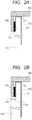
- FIG. 2A and FIG. 2B Other examples of the structure of the insulating tube and a part of the anode member around the outer circumferential tubular portion are described with reference to FIG. 2A and FIG. 2B .
- the outer circumferential conductive film 114 that is electrically connected to the end surface conductive film 113 is formed on the circumferential surface of the insulating tube 110 on the anode member 43 side.
- the outer circumferential conductive film 114 is electrically connected to the outer circumferential tubular portion 43b.
- the joining member 115 hermetically joins the insulating tube 110 and the anode member 43 as in the embodiment described with reference to FIG. 1A to FIG. 1C .
- the joining member 115 is sandwiched between the insulating tube 110 and the outer circumferential tubular portion 43b, in the state in which the outer circumferential conductive film 114 formed on the circumferential surface of the insulating tube 110 is sandwiched between the joining member 115 and the insulating tube 110.
- Forming the outer circumferential conductive film 114 improves the reliability of electrical connection between the inner circumferential conductive film 112 and the anode member 43 even more.
- the outer circumferential conductive film 114 may be formed intermittently in the tube circumference direction of the insulating tube 110 by extending the end surface conductive film 113 toward the circumference of the insulating tube 110, but it is preferred to form the outer circumferential conductive film 114 continuously along the entire circumference of the insulating tube 110 in order to facilitate the close fitting of the joining member 115 free of a gap. It is also preferred to form the outer circumferential conductive film 114 and the end surface conductive film 113 as a continuous film in order to ensure electrical connection therebetween.
- the insulating tube 110 is preferred to have a ring-shaped region where the outer tube diameter increases in a tube axis direction that runs from an end of the insulating tube 110 on the anode member 43 side toward the other end of the insulating tube 110 on the cathode member 41 side.
- the ring-shaped region in the embodiment of FIG. 2B is a ring-shaped level difference 110a, which surrounds the inner circumferential conductive film 112.
- the level difference 110a formed on the circumferential surface of the insulating tube 110 makes the outer diameter of the insulating tube 110 in a region of the insulating tube 110 on the cathode member 41 side larger than in its adjacent region on the anode member 43 side.
- the outer circumferential tubular portion 43b faces the region on the anode member 43 side where the outer diameter is smaller, and the joining member 115 is sandwiched between the circumferential surface of the region where the outer diameter of the insulating tube 110 is smaller and the outer circumferential tubular portion 43b.
- the level difference 110a dams up the joining member 115 that is melted for the joining by way of the joining member 115 and is flowing, and prevents the melted joining member 115 from flowing beyond the level difference 110a toward the cathode member 41 and impairing the withstand voltage between the cathode 51 and the anode 52.
- the outer circumferential conductive film 114 is formed in FIG. 2A and FIG. 2B , the X-ray generating tube 102 may not include the outer circumferential conductive film 114.
- FIG. 3 is a diagram of an X-ray generating apparatus 101 according to the embodiment of the present invention, which is configured to take the X-ray beam 11 out to the front of an X-ray transmitting window 121.
- the X-ray generating apparatus 101 includes, in a container 120 where the X-ray transmitting window 121 is installed, the X-ray generating tube 102 and the drive circuit 103 for driving the X-ray generating tube 102.
- the drive circuit 103 applies a tube voltage Va between the cathode 51 and the anode 52 to form an accelerating electric field between the target layer 22 and the electron emitting portion 2.
- the tube voltage Va that is suitable for the thickness of the target layer 22 and the type of metal forming the target layer 22, an X-ray type necessary for imaging can be selected.
- the container 120 which houses the X-ray generating tube 102 and the drive circuit 103, desirably has strength sufficient as a container and excellent heat dissipating properties.
- the constituent material of the container 120 is, for example, a metal material such as brass, iron, or stainless steel.
- the insulating liquid 109 is a liquid having electrical insulation properties, maintains electrical insulation inside the container 120, and serves as a cooling medium for the X-ray generating tube 102.
- An electrical insulation oil such as a mineral oil, a silicone oil, or a perfluoro-based oil is preferred as the insulating liquid 109.
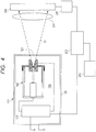
- a structural example of a radiography system 60 which includes the X-ray generating tube 102 of the present invention, is described next with reference to FIG. 4 .
- a system control unit 202 controls the X-ray generating apparatus 101 and an X-ray detector 206 in an integrated manner.
- the drive circuit 103 outputs, under control of the system control unit 202, various control signals to the X-ray generating tube 102.
- the control signals output by the drive circuit 103 are used to control the emission state of the X-ray beam 11 emitted from the X-ray generating apparatus 101.
- the X-ray beam 11 emitted from the X-ray generating apparatus 101 is adjusted in irradiation range by a collimator unit (not shown) having a variable aperture, emitted to the outside of the X-ray generating apparatus 101, transmitted through a subject to be examined 204 (hereinafter referred to as simply "subject"), and detected by the detector 206.
- the detector 206 converts the detected X-ray into image signals, which are output to a signal processing portion 205.
- the signal processing portion 205 performs, under control of the system control unit 202, given signal processing on the image signals, and outputs the processed image signals to the system control unit 202.
- the system control unit 202 Based on the processed image signals, the system control unit 202 outputs display signals for displaying an image on a display apparatus 203.
- the display apparatus 203 displays on a screen an image based on the display signals as a photographed image of the subject 204.
- the radiography system 60 of the present invention is applicable to non-destructive testing of an industrial product, and the diagnosis of human and animal pathology.
- the X-ray generating tube 102 having the insulating tube 110 of FIG. 1A to FIG. 1C and the joining structure of FIG. 1A to FIG. 1C for joining the anode member 43 to the insulating tube 110 was manufactured and mounted to the X-ray generating apparatus 101.
- the inner circumferential conductive film 112 was formed from a Ti-Cu-based material used as a ceramic metalizing material, on the inner circumferential surface of the insulating tube 110 that was made of alumina on the anode 52 side.
- the end surface conductive films 113 each having a width of 2 mm and continuous from the inner circumferential conductive film 112 were formed in four places on the end surface of the insulating tube 110 on the anode 52 side with use of the same material as the inner circumferential conductive film 112.
- the inner circumferential conductive film 112 and the end surface conductive films 113 were formed by preparing a paste that contained Ti-Cu-based powder, applying the paste directly to the insulating tube 110, drying the applied paste, and then executing vacuum heat treatment at 1,000°C.
- the thickness of the inner circumferential conductive film 112 and the end surface conductive films 113 after the heat treatment was 8 ⁇ m on average.
- a silver brazing filler metal paste containing Ti was next applied to a part of the circumference of the insulating tube 110 that was in contact with the outer circumferential tubular portion 43b, and dried. Thereafter, components were arranged so as to bring the anode member 43 into contact with the end surface conductive films 113 formed on the insulating tube 110, and to bring the outer circumferential tubular portion 43b into contact with the joining member 115 formed on the circumference of the insulating tube 110, and vacuum heat treatment was executed at 800°C for brazing. In the heat treatment, a weight was put on the anode member 43 in order to help along press-fit between the end surface conductive films 113 and the anode member 43. The metallization of alumina and hermetical brazing were accomplished by using brazing filler metal that contained Ti. The material used for the anode member 43 and the outer circumferential tubular portion 43ba was Kovar.
- the X-ray generating tube 102 of Example 1 was mounted to the radiography system 60 of FIG. 4 , and changes in X-ray output were evaluated.
- the X-ray generating tube 102 was driven to evaluate changes with time of the position of the focal spot 11a of the X-ray beam 11. A favorable result was obtained in which the change in the center position of the focal spot 11a was 10 ⁇ m or less. The evaluation was made without placing the subject 204.
- Example 2 For comparison with Example 1, the X-ray generating tube 102 that had no end surface conductive film 113 was manufactured. The rest of the structure and the method used to manufacture this X-ray generating tube 102 were the same as those in Example 1.
- the X-ray generating tube 102 having the insulating tube 110 of FIG. 2B and the joining structure of FIG. 2B for joining the anode member 43 to the insulating tube 110 was manufactured and mounted to the X-ray generating apparatus 101.
- the inner circumferential conductive film 112 and the end surface conductive films 113 were formed from a Ti-Cu-based material, and the same material and the same method were used to form the outer circumferential conductive film 114 on the circumferential surface of the insulating tube 110 so as to be continuous from the end surface conductive films 113.
- a silver brazing filler metal wire was wound as the joining member 115 around the circumference of the insulating tube 110 in a part closer to the anode member 43 than the level difference 110a.
- components were arranged so as to bring the anode member 43 into contact with the end surface conductive films 113 formed on the insulating tube 110, and to bring the sleeve 43a into contact with the brazing filler metal 115 formed on the circumference of the insulating tube 110, and vacuum heat treatment was executed at 800°C for brazing.
- a weight was put on the anode member 43 in order to help along press-fit between the end surface conductive films 113 and the anode member 43.
- the Ti-Cu-based outer circumferential conductive film 114 also acted to metallize alumina, and hermetical brazing was thus accomplished.
- Kovar was used as the material of the anode member 43.
- a groove portion (not shown) for holding the wire may be formed in the insulating tube 110 and the wire may be arranged in the groove portion.
- Example 2 the X-ray generating tube 102 of Example 2 was mounted to the radiography system 60, and changes in X-ray output were evaluated. A favorable result was obtained in which the change in the center position of the focal spot was 10 ⁇ m or less.
- Example 3 the X-ray generating apparatus 101 of Example 1 was used to construct the radiography system 60 of FIG. 4 .
- electrical connection is made between the inner circumferential conductive film and the anode member via the end surface conductive film, which is sandwiched between an end surface of the insulating tube at one end and the anode member and which is electrically connected to the anode member.
- This improves the reliability of electrical connection between the inner circumferential conductive film and the anode member, and prevents without fail the charging of the inner surface of the insulating tube, thereby providing an X-ray generating tube that is reduced in changes in X-ray output.
- an X-ray generating apparatus and a radiography system that include the highly reliable X-ray generating tube reduced in changes in X-ray output can be provided.
- An X-ray generating tube includes: an anode including a target and an anode member electrically connected to the target; a cathode including an electron emitting source and a cathode member electrically connected to the electron emitting source; and an insulating tube joined at one end to the anode member and joined at the other end to the cathode member so that the target and the electron emitting portion face each other, in which an inner circumferential conductive film is formed on an inner surface of the insulating tube; an end surface conductive film extends from one edge of the inner circumferential conductive film on the one end side onto a surface of the one end of the insulating tube; and the end surface conductive film is sandwiched between the end surface and the anode member to be electrically connected to the anode member.
Landscapes
- X-Ray Techniques (AREA)
Applications Claiming Priority (1)
| Application Number | Priority Date | Filing Date | Title |
|---|---|---|---|
| JP2014220083A JP6415250B2 (ja) | 2014-10-29 | 2014-10-29 | X線発生管、x線発生装置及びx線撮影システム |
Publications (2)
| Publication Number | Publication Date |
|---|---|
| EP3016129A1 EP3016129A1 (en) | 2016-05-04 |
| EP3016129B1 true EP3016129B1 (en) | 2017-08-30 |
Family
ID=54359974
Family Applications (1)
| Application Number | Title | Priority Date | Filing Date |
|---|---|---|---|
| EP15190789.6A Active EP3016129B1 (en) | 2014-10-29 | 2015-10-21 | X-ray generating tube, x-ray generating apparatus, and radiography system |
Country Status (4)
| Country | Link |
|---|---|
| US (2) | US9824848B2 (ja) |
| EP (1) | EP3016129B1 (ja) |
| JP (1) | JP6415250B2 (ja) |
| CN (1) | CN105575747B (ja) |
Families Citing this family (13)
| Publication number | Priority date | Publication date | Assignee | Title |
|---|---|---|---|---|
| JP6573380B2 (ja) * | 2015-07-27 | 2019-09-11 | キヤノン株式会社 | X線発生装置及びx線撮影システム |
| JP6055069B1 (ja) | 2015-12-10 | 2016-12-27 | サンアロー株式会社 | 臓器、組織又は器官モデル |
| JP6667366B2 (ja) * | 2016-05-23 | 2020-03-18 | キヤノン株式会社 | X線発生管、x線発生装置、およびx線撮影システム |
| FR3069100B1 (fr) * | 2017-07-11 | 2019-08-23 | Thales | Source generatrice de rayons ionisants compacte, ensemble comprenant plusieurs sources et procede de realisation de la source |
| FR3069099B1 (fr) * | 2017-07-11 | 2023-07-21 | Thales Sa | Source generatrice de rayons ionisants compacte, ensemble comprenant plusieurs sources et procede de realisation de la source |
| WO2019049208A1 (ja) * | 2017-09-05 | 2019-03-14 | 株式会社島津製作所 | X線発生装置用ターゲット、このx線発生装置用ターゲットを備えたx線発生装置、および、x線発生装置用ターゲットの製造方法 |
| JP2019114405A (ja) * | 2017-12-22 | 2019-07-11 | キヤノン電子管デバイス株式会社 | X線管及びx線管の製造方法 |
| JP7048396B2 (ja) * | 2018-04-12 | 2022-04-05 | 浜松ホトニクス株式会社 | X線管 |
| CN109786193A (zh) * | 2018-12-29 | 2019-05-21 | 同方威视技术股份有限公司 | 一种x射线源 |
| EP3923312B1 (en) * | 2019-04-15 | 2024-04-24 | Canon Anelva Corporation | X-ray generation device and x-ray imaging device |
| JP7196039B2 (ja) * | 2019-08-27 | 2022-12-26 | キヤノン電子管デバイス株式会社 | X線管の製造方法 |
| US11688578B2 (en) * | 2020-11-11 | 2023-06-27 | Moxtek, Inc. | Interruption-ring in an X-ray tube |
| JP7486694B1 (ja) | 2023-01-25 | 2024-05-17 | キヤノンアネルバ株式会社 | X線発生装置およびx線撮像装置 |
Family Cites Families (8)
| Publication number | Priority date | Publication date | Assignee | Title |
|---|---|---|---|---|
| JPS5736735A (ja) * | 1980-08-13 | 1982-02-27 | Hitachi Ltd | Kodenatsuzetsuenshinkuyoki |
| JPS5844662A (ja) * | 1981-09-09 | 1983-03-15 | Hitachi Ltd | セラミツク外囲器x線管 |
| JPS59162771U (ja) * | 1983-04-15 | 1984-10-31 | 株式会社東芝 | X線管 |
| JP2000251776A (ja) * | 1999-02-25 | 2000-09-14 | Canon Inc | 画像形成装置 |
| US6658086B2 (en) | 2001-06-19 | 2003-12-02 | Carl Zeiss | Optically driven therapeutic radiation source with voltage gradient control |
| US8280007B2 (en) | 2010-10-26 | 2012-10-02 | General Electric Company | Apparatus and method for improved transient response in an electromagnetically controlled X-ray tube |
| JP6049350B2 (ja) * | 2012-08-21 | 2016-12-21 | キヤノン株式会社 | 放射線発生管、放射線発生ユニット及び放射線撮影システム |
| JP6308714B2 (ja) * | 2012-08-28 | 2018-04-11 | キヤノン株式会社 | 放射線発生管および該放射線発生管を備えた放射線発生装置 |
-
2014
- 2014-10-29 JP JP2014220083A patent/JP6415250B2/ja active Active
-
2015
- 2015-10-14 US US14/882,562 patent/US9824848B2/en active Active
- 2015-10-21 EP EP15190789.6A patent/EP3016129B1/en active Active
- 2015-10-26 CN CN201510700386.1A patent/CN105575747B/zh active Active
-
2017
- 2017-10-12 US US15/782,186 patent/US10381190B2/en active Active
Non-Patent Citations (1)
| Title |
|---|
| None * |
Also Published As
| Publication number | Publication date |
|---|---|
| CN105575747B (zh) | 2017-12-05 |
| US9824848B2 (en) | 2017-11-21 |
| US20180053624A1 (en) | 2018-02-22 |
| JP6415250B2 (ja) | 2018-10-31 |
| US10381190B2 (en) | 2019-08-13 |
| US20160126053A1 (en) | 2016-05-05 |
| CN105575747A (zh) | 2016-05-11 |
| EP3016129A1 (en) | 2016-05-04 |
| JP2016085945A (ja) | 2016-05-19 |
Similar Documents
| Publication | Publication Date | Title |
|---|---|---|
| US10381190B2 (en) | X-ray generating tube, X-ray generating apparatus, and radiography system | |
| EP2751828B1 (en) | Target structure and x-ray generating apparatus | |
| US9653252B2 (en) | X-ray generating tube, X-ray generating apparatus and X-ray imaging system using the same | |
| US9117621B2 (en) | Radiation generating tube, radiation generating unit, and radiation image taking system | |
| CN105655216B (zh) | X射线发生管、x射线发生装置和射线照相系统 | |
| JP2016085945A5 (ja) | ||
| US9831060B2 (en) | X-ray generating apparatus and radiography system using the same | |
| US10062539B2 (en) | Anode and x-ray generating tube, x-ray generating apparatus, and radiography system that use the anode | |
| US20140177796A1 (en) | X-ray tube | |
| US10242837B2 (en) | Anode and X-ray generating tube, X-ray generating apparatus, and radiography system that use the anode | |
| US11114268B2 (en) | X-ray generating tube, X-ray generating apparatus, and radiography system | |
| JP6580231B2 (ja) | X線発生管、x線発生装置及びx線撮影システム | |
| JP4263861B2 (ja) | X線管およびその製造方法 | |
| RU2459307C1 (ru) | Импульсная рентгеновская трубка | |
| JP6272539B1 (ja) | X線発生管及びそれを用いたx線発生装置とx線撮影システム | |
| JP6611495B2 (ja) | X線発生管、x線発生装置およびx線撮影システム | |
| JP2016085946A (ja) | X線発生管、x線発生装置及びx線撮影システム | |
| JP2015153548A (ja) | 放射線管とこれを用いた放射線発生装置、放射線撮影システム、及び放射線管の製造方法 |
Legal Events
| Date | Code | Title | Description |
|---|---|---|---|
| PUAI | Public reference made under article 153(3) epc to a published international application that has entered the european phase |
Free format text: ORIGINAL CODE: 0009012 |
|
| AK | Designated contracting states |
Kind code of ref document: A1 Designated state(s): AL AT BE BG CH CY CZ DE DK EE ES FI FR GB GR HR HU IE IS IT LI LT LU LV MC MK MT NL NO PL PT RO RS SE SI SK SM TR |
|
| AX | Request for extension of the european patent |
Extension state: BA ME |
|
| 17P | Request for examination filed |
Effective date: 20161104 |
|
| RBV | Designated contracting states (corrected) |
Designated state(s): AL AT BE BG CH CY CZ DE DK EE ES FI FR GB GR HR HU IE IS IT LI LT LU LV MC MK MT NL NO PL PT RO RS SE SI SK SM TR |
|
| GRAP | Despatch of communication of intention to grant a patent |
Free format text: ORIGINAL CODE: EPIDOSNIGR1 |
|
| INTG | Intention to grant announced |
Effective date: 20170313 |
|
| RIN1 | Information on inventor provided before grant (corrected) |
Inventor name: IKARASHI, YOICHI |
|
| GRAS | Grant fee paid |
Free format text: ORIGINAL CODE: EPIDOSNIGR3 |
|
| GRAA | (expected) grant |
Free format text: ORIGINAL CODE: 0009210 |
|
| AK | Designated contracting states |
Kind code of ref document: B1 Designated state(s): AL AT BE BG CH CY CZ DE DK EE ES FI FR GB GR HR HU IE IS IT LI LT LU LV MC MK MT NL NO PL PT RO RS SE SI SK SM TR |
|
| REG | Reference to a national code |
Ref country code: GB Ref legal event code: FG4D |
|
| REG | Reference to a national code |
Ref country code: CH Ref legal event code: EP |
|
| REG | Reference to a national code |
Ref country code: AT Ref legal event code: REF Ref document number: 924363 Country of ref document: AT Kind code of ref document: T Effective date: 20170915 |
|
| REG | Reference to a national code |
Ref country code: IE Ref legal event code: FG4D |
|
| REG | Reference to a national code |
Ref country code: DE Ref legal event code: R096 Ref document number: 602015004430 Country of ref document: DE |
|
| REG | Reference to a national code |
Ref country code: NL Ref legal event code: MP Effective date: 20170830 |
|
| REG | Reference to a national code |
Ref country code: LT Ref legal event code: MG4D |
|
| REG | Reference to a national code |
Ref country code: AT Ref legal event code: MK05 Ref document number: 924363 Country of ref document: AT Kind code of ref document: T Effective date: 20170830 |
|
| PG25 | Lapsed in a contracting state [announced via postgrant information from national office to epo] |
Ref country code: NO Free format text: LAPSE BECAUSE OF FAILURE TO SUBMIT A TRANSLATION OF THE DESCRIPTION OR TO PAY THE FEE WITHIN THE PRESCRIBED TIME-LIMIT Effective date: 20171130 Ref country code: LT Free format text: LAPSE BECAUSE OF FAILURE TO SUBMIT A TRANSLATION OF THE DESCRIPTION OR TO PAY THE FEE WITHIN THE PRESCRIBED TIME-LIMIT Effective date: 20170830 Ref country code: SE Free format text: LAPSE BECAUSE OF FAILURE TO SUBMIT A TRANSLATION OF THE DESCRIPTION OR TO PAY THE FEE WITHIN THE PRESCRIBED TIME-LIMIT Effective date: 20170830 Ref country code: AT Free format text: LAPSE BECAUSE OF FAILURE TO SUBMIT A TRANSLATION OF THE DESCRIPTION OR TO PAY THE FEE WITHIN THE PRESCRIBED TIME-LIMIT Effective date: 20170830 Ref country code: HR Free format text: LAPSE BECAUSE OF FAILURE TO SUBMIT A TRANSLATION OF THE DESCRIPTION OR TO PAY THE FEE WITHIN THE PRESCRIBED TIME-LIMIT Effective date: 20170830 Ref country code: FI Free format text: LAPSE BECAUSE OF FAILURE TO SUBMIT A TRANSLATION OF THE DESCRIPTION OR TO PAY THE FEE WITHIN THE PRESCRIBED TIME-LIMIT Effective date: 20170830 |
|
| PG25 | Lapsed in a contracting state [announced via postgrant information from national office to epo] |
Ref country code: IS Free format text: LAPSE BECAUSE OF FAILURE TO SUBMIT A TRANSLATION OF THE DESCRIPTION OR TO PAY THE FEE WITHIN THE PRESCRIBED TIME-LIMIT Effective date: 20171230 Ref country code: LV Free format text: LAPSE BECAUSE OF FAILURE TO SUBMIT A TRANSLATION OF THE DESCRIPTION OR TO PAY THE FEE WITHIN THE PRESCRIBED TIME-LIMIT Effective date: 20170830 Ref country code: GR Free format text: LAPSE BECAUSE OF FAILURE TO SUBMIT A TRANSLATION OF THE DESCRIPTION OR TO PAY THE FEE WITHIN THE PRESCRIBED TIME-LIMIT Effective date: 20171201 Ref country code: ES Free format text: LAPSE BECAUSE OF FAILURE TO SUBMIT A TRANSLATION OF THE DESCRIPTION OR TO PAY THE FEE WITHIN THE PRESCRIBED TIME-LIMIT Effective date: 20170830 Ref country code: RS Free format text: LAPSE BECAUSE OF FAILURE TO SUBMIT A TRANSLATION OF THE DESCRIPTION OR TO PAY THE FEE WITHIN THE PRESCRIBED TIME-LIMIT Effective date: 20170830 Ref country code: BG Free format text: LAPSE BECAUSE OF FAILURE TO SUBMIT A TRANSLATION OF THE DESCRIPTION OR TO PAY THE FEE WITHIN THE PRESCRIBED TIME-LIMIT Effective date: 20171130 |
|
| PG25 | Lapsed in a contracting state [announced via postgrant information from national office to epo] |
Ref country code: NL Free format text: LAPSE BECAUSE OF FAILURE TO SUBMIT A TRANSLATION OF THE DESCRIPTION OR TO PAY THE FEE WITHIN THE PRESCRIBED TIME-LIMIT Effective date: 20170830 |
|
| PG25 | Lapsed in a contracting state [announced via postgrant information from national office to epo] |
Ref country code: DK Free format text: LAPSE BECAUSE OF FAILURE TO SUBMIT A TRANSLATION OF THE DESCRIPTION OR TO PAY THE FEE WITHIN THE PRESCRIBED TIME-LIMIT Effective date: 20170830 Ref country code: CZ Free format text: LAPSE BECAUSE OF FAILURE TO SUBMIT A TRANSLATION OF THE DESCRIPTION OR TO PAY THE FEE WITHIN THE PRESCRIBED TIME-LIMIT Effective date: 20170830 Ref country code: PL Free format text: LAPSE BECAUSE OF FAILURE TO SUBMIT A TRANSLATION OF THE DESCRIPTION OR TO PAY THE FEE WITHIN THE PRESCRIBED TIME-LIMIT Effective date: 20170830 Ref country code: RO Free format text: LAPSE BECAUSE OF FAILURE TO SUBMIT A TRANSLATION OF THE DESCRIPTION OR TO PAY THE FEE WITHIN THE PRESCRIBED TIME-LIMIT Effective date: 20170830 |
|
| PG25 | Lapsed in a contracting state [announced via postgrant information from national office to epo] |
Ref country code: IT Free format text: LAPSE BECAUSE OF FAILURE TO SUBMIT A TRANSLATION OF THE DESCRIPTION OR TO PAY THE FEE WITHIN THE PRESCRIBED TIME-LIMIT Effective date: 20170830 Ref country code: SK Free format text: LAPSE BECAUSE OF FAILURE TO SUBMIT A TRANSLATION OF THE DESCRIPTION OR TO PAY THE FEE WITHIN THE PRESCRIBED TIME-LIMIT Effective date: 20170830 Ref country code: SM Free format text: LAPSE BECAUSE OF FAILURE TO SUBMIT A TRANSLATION OF THE DESCRIPTION OR TO PAY THE FEE WITHIN THE PRESCRIBED TIME-LIMIT Effective date: 20170830 Ref country code: EE Free format text: LAPSE BECAUSE OF FAILURE TO SUBMIT A TRANSLATION OF THE DESCRIPTION OR TO PAY THE FEE WITHIN THE PRESCRIBED TIME-LIMIT Effective date: 20170830 Ref country code: MC Free format text: LAPSE BECAUSE OF FAILURE TO SUBMIT A TRANSLATION OF THE DESCRIPTION OR TO PAY THE FEE WITHIN THE PRESCRIBED TIME-LIMIT Effective date: 20170830 |
|
| REG | Reference to a national code |
Ref country code: DE Ref legal event code: R097 Ref document number: 602015004430 Country of ref document: DE |
|
| PLBE | No opposition filed within time limit |
Free format text: ORIGINAL CODE: 0009261 |
|
| STAA | Information on the status of an ep patent application or granted ep patent |
Free format text: STATUS: NO OPPOSITION FILED WITHIN TIME LIMIT |
|
| REG | Reference to a national code |
Ref country code: IE Ref legal event code: MM4A |
|
| REG | Reference to a national code |
Ref country code: FR Ref legal event code: ST Effective date: 20180629 |
|
| PG25 | Lapsed in a contracting state [announced via postgrant information from national office to epo] |
Ref country code: LU Free format text: LAPSE BECAUSE OF NON-PAYMENT OF DUE FEES Effective date: 20171021 |
|
| 26N | No opposition filed |
Effective date: 20180531 |
|
| REG | Reference to a national code |
Ref country code: BE Ref legal event code: MM Effective date: 20171031 |
|
| PG25 | Lapsed in a contracting state [announced via postgrant information from national office to epo] |
Ref country code: BE Free format text: LAPSE BECAUSE OF NON-PAYMENT OF DUE FEES Effective date: 20171031 Ref country code: SI Free format text: LAPSE BECAUSE OF FAILURE TO SUBMIT A TRANSLATION OF THE DESCRIPTION OR TO PAY THE FEE WITHIN THE PRESCRIBED TIME-LIMIT Effective date: 20170830 Ref country code: FR Free format text: LAPSE BECAUSE OF NON-PAYMENT OF DUE FEES Effective date: 20171031 |
|
| PG25 | Lapsed in a contracting state [announced via postgrant information from national office to epo] |
Ref country code: MT Free format text: LAPSE BECAUSE OF NON-PAYMENT OF DUE FEES Effective date: 20171021 |
|
| PG25 | Lapsed in a contracting state [announced via postgrant information from national office to epo] |
Ref country code: IE Free format text: LAPSE BECAUSE OF NON-PAYMENT OF DUE FEES Effective date: 20171021 |
|
| REG | Reference to a national code |
Ref country code: CH Ref legal event code: PL |
|
| PG25 | Lapsed in a contracting state [announced via postgrant information from national office to epo] |
Ref country code: HU Free format text: LAPSE BECAUSE OF FAILURE TO SUBMIT A TRANSLATION OF THE DESCRIPTION OR TO PAY THE FEE WITHIN THE PRESCRIBED TIME-LIMIT; INVALID AB INITIO Effective date: 20151021 |
|
| PG25 | Lapsed in a contracting state [announced via postgrant information from national office to epo] |
Ref country code: LI Free format text: LAPSE BECAUSE OF NON-PAYMENT OF DUE FEES Effective date: 20181031 Ref country code: CH Free format text: LAPSE BECAUSE OF NON-PAYMENT OF DUE FEES Effective date: 20181031 |
|
| PG25 | Lapsed in a contracting state [announced via postgrant information from national office to epo] |
Ref country code: CY Free format text: LAPSE BECAUSE OF FAILURE TO SUBMIT A TRANSLATION OF THE DESCRIPTION OR TO PAY THE FEE WITHIN THE PRESCRIBED TIME-LIMIT Effective date: 20170830 |
|
| PG25 | Lapsed in a contracting state [announced via postgrant information from national office to epo] |
Ref country code: MK Free format text: LAPSE BECAUSE OF FAILURE TO SUBMIT A TRANSLATION OF THE DESCRIPTION OR TO PAY THE FEE WITHIN THE PRESCRIBED TIME-LIMIT Effective date: 20170830 |
|
| PG25 | Lapsed in a contracting state [announced via postgrant information from national office to epo] |
Ref country code: TR Free format text: LAPSE BECAUSE OF FAILURE TO SUBMIT A TRANSLATION OF THE DESCRIPTION OR TO PAY THE FEE WITHIN THE PRESCRIBED TIME-LIMIT Effective date: 20170830 |
|
| PG25 | Lapsed in a contracting state [announced via postgrant information from national office to epo] |
Ref country code: PT Free format text: LAPSE BECAUSE OF FAILURE TO SUBMIT A TRANSLATION OF THE DESCRIPTION OR TO PAY THE FEE WITHIN THE PRESCRIBED TIME-LIMIT Effective date: 20170830 |
|
| PG25 | Lapsed in a contracting state [announced via postgrant information from national office to epo] |
Ref country code: AL Free format text: LAPSE BECAUSE OF FAILURE TO SUBMIT A TRANSLATION OF THE DESCRIPTION OR TO PAY THE FEE WITHIN THE PRESCRIBED TIME-LIMIT Effective date: 20170830 |
|
| GBPC | Gb: european patent ceased through non-payment of renewal fee |
Effective date: 20191021 |
|
| PG25 | Lapsed in a contracting state [announced via postgrant information from national office to epo] |
Ref country code: GB Free format text: LAPSE BECAUSE OF NON-PAYMENT OF DUE FEES Effective date: 20191021 |
|
| PGFP | Annual fee paid to national office [announced via postgrant information from national office to epo] |
Ref country code: DE Payment date: 20230920 Year of fee payment: 9 |