EP3008820B1 - Self-biased receiver - Google Patents
Self-biased receiver Download PDFInfo
- Publication number
- EP3008820B1 EP3008820B1 EP14736560.5A EP14736560A EP3008820B1 EP 3008820 B1 EP3008820 B1 EP 3008820B1 EP 14736560 A EP14736560 A EP 14736560A EP 3008820 B1 EP3008820 B1 EP 3008820B1
- Authority
- EP
- European Patent Office
- Prior art keywords
- amplifier
- circuit
- transistor
- bias
- bias current
- Prior art date
- Legal status (The legal status is an assumption and is not a legal conclusion. Google has not performed a legal analysis and makes no representation as to the accuracy of the status listed.)
- Active
Links
Images


Classifications
-
- H—ELECTRICITY
- H03—ELECTRONIC CIRCUITRY
- H03F—AMPLIFIERS
- H03F3/00—Amplifiers with only discharge tubes or only semiconductor devices as amplifying elements
- H03F3/189—High-frequency amplifiers, e.g. radio frequency amplifiers
- H03F3/19—High-frequency amplifiers, e.g. radio frequency amplifiers with semiconductor devices only
- H03F3/193—High-frequency amplifiers, e.g. radio frequency amplifiers with semiconductor devices only with field-effect devices
-
- H—ELECTRICITY
- H03—ELECTRONIC CIRCUITRY
- H03F—AMPLIFIERS
- H03F1/00—Details of amplifiers with only discharge tubes, only semiconductor devices or only unspecified devices as amplifying elements
- H03F1/30—Modifications of amplifiers to reduce influence of variations of temperature or supply voltage or other physical parameters
- H03F1/301—Modifications of amplifiers to reduce influence of variations of temperature or supply voltage or other physical parameters in MOSFET amplifiers
Definitions
- the present disclosure relates generally to electronic circuits, and more particularly, to a self-biased receiver.
- the integrated circuit is generally designed with a large number of standard cells distributed across the "core" of the chip. Each cell is formed with any numbers of transistors that work together to provide a functional unit. These cells are interconnected together to form an operational device.
- the core is surrounded by a number of larger cells arranged along the periphery of the chip.
- the larger cells contain input/output (I/O) drivers formed with transistors having wider channel lengths, thicker oxide layers, and higher threshold voltages to interface with higher voltage off-chip devices.
- I/O driver is a self-biased differential receiver.
- the self-biased receiver performs well in the presence of process, voltage and temperature (“PVT”) variations, but may exhibit intersymbol interference (“ISI”) jitter and duty cycle distortion (“DCD”) when the operating voltage is reduced in a power savings mode.
- ISI intersymbol interference
- DCD duty cycle distortion
- the ISI jitter and DCD can reduce the usable data rate for the self-biased differential receiver.
- the differential amplifier improves output voltage swings and gain without the need for additional circuits for driving current sources or voltage sources.
- the differential amplifier includes a first current source, a second current source, a first inverter, a second inverter and a self bias control circuit.
- the first current source and the second current source provide a first bias current and a second bias current.
- the self bias control circuit maintains the first bias current and the second bias current at a constant level. Therefore, the differential amplifier provides constant current without additional circuits for driving current sources or voltage sources, and achieves a wider range of voltage output swings and a higher gain, as compared to conventional differential amplifier configurations.
- One aspect of a receiver includes an amplifier and a bias circuit configured to provide bias current to the amplifier in response to a bias voltage produced by the amplifier, wherein the bias circuit includes a first circuit configured to provide self biasing of the receiver by adjusting the bias current using the feedback from the amplifier and a second circuit configured to further adjust the bias current using additional feedback from the amplifier.
- One aspect of a method of receiving a signal includes providing a bias current to an amplifier from a bias circuit in response to a bias voltage produced by the amplifier, wherein the bias circuit includes a first circuit configured to provide self biasing of the receiver by adjusting the bias current using the feedback from the amplifier and a second circuit configured to further adjust the bias current using additional feedback from the amplifier.
- a receiver includes an amplifying means for amplifying a signal, and a biasing means for providing a bias current to the amplifying means in response to a bias voltage produced by the amplifier, wherein the biasing means includes a first circuit means for providing self biasing of the receiver by adjusting the bias current using the feedback from the amplifier and a second circuit means for adjusting the bias current using additional feedback from the amplifying means.
- any of these circuits may be implemented as an integrated circuit, or as part of the design of an integrated circuit.
- the integrated circuit may be an end product, such as a microprocessor, a digital signal processor (DSP), an application specific integrated circuit (ASIC), programmable logic, memory, or any other suitable integrated circuitry.
- the integrated circuit may be integrated with other chips, discrete circuit elements, and/or other components as part of either an intermediate product, such as a motherboard, or an end product.
- the end product can be any suitable product that includes integrated circuits, including by way of example, a cellular phone, a personal digital assistant (PDA), laptop computer, a desktop computer (PC), a computer peripheral device, a multimedia device, a video device, an audio device, a global positioning system (GPS), a wireless sensor, or any other suitable device.
- a cellular phone a personal digital assistant (PDA), laptop computer, a desktop computer (PC), a computer peripheral device, a multimedia device, a video device, an audio device, a global positioning system (GPS), a wireless sensor, or any other suitable device.
- PDA personal digital assistant
- PC desktop computer
- GPS global positioning system
- wireless sensor or any other suitable device.
- FIG. 1 a functional block diagram illustrating an example of a receiver is shown.
- the receiver 100 includes an amplifier 102.
- the amplifier 102 provides a means for amplifying a signal.
- the amplifier 102 may be implemented as a differential amplifier to increase the common mode rejection ratio (CMRR), but may be implemented differently for other applications.
- CMRR common mode rejection ratio
- the differential amplifier may be configured to have either a differential or a single-ended output depending upon the particular application and overall design constraints.
- the receiver 100 also includes a bias circuit 104.
- the bias circuit 104 provides a means for providing a bias current to the amplifier 102.
- the receiver 100 may be self-biased. That is, the bias circuit 104 receives its bias voltage from the differential amplifier 102 in the form of negative feedback. Alternatively, the receiver 100 may have a fixed bias circuit which receives its bias voltage from a voltage source independent of the differential amplifier.
- the bias circuit 104 may also use feedback from the output of amplifier 102 to increase the bias current provided to the amplifier 102. The increased bias current may tend to reduce ISI jitter and DCD when the operating voltage is reduced in a power savings mode.
- FIG. 2 is a schematic diagram illustrating an example of a receiver 200 with an amplifier 226 and a bias circuit 224.
- the amplifier 226 is implemented as a differential amplifier, but may be implemented differently in other embodiments.
- the differential amplifier 226 includes a first amplifier 228 and a second amplifier 230 that operate together to amplify the difference between the voltage of an input signal 202 and a reference voltage V ref .
- the first amplifier 228 is shown as a CMOS amplifier with PMOS transistor 204, an NMOS transistor 206, a signal input 202, and an output 222 that is provided to an inverter 216.
- the inverter 216 provides a single-ended output to a remote circuit or load.
- the second amplifier 230 is also shown as a CMOS amplifier with a PMOS transistor 212, an NMOS transistor 214, and an input tied to the reference voltage V ref .
- the output from the second amplifier 230 provides a bias voltage 220 which is applied to the bias circuit 224.
- the bias circuit 224 includes a circuit comprising a PMOS transistor 208 and an NMOS transistor 210.
- the PMOS transistor 208 is coupled between the positive supply rail V DD and the amplifier 226 and the NMOS transistor 210 is coupled between the amplifier 226 and the negative supply rail V SS .
- the bias voltage 220 from the amplifier 226 is fed back to the gates of the PMOS transistor 208 and the NMOS transistor 210 bias to the transistors 204, 206, 212, 214 in the amplifier 226.
- the voltage V ref may be biased as half of VDD.
- bias voltage 220 By coupling the bias voltage 220 to the gates of the PMOS transistor 208 and the NMOS transistor 210, a negative feedback loop is created that stabilizes the bias voltage 220. Any increase in the bias voltage 220 due to PVT effects will increase the gate-to-source voltage V GS of the NMOS transistor 210. This will reduce the "on" resistance of the NMOS transistor 210, which in turn will pull down the bias voltage 220 towards the negative supply rail V SS . Conversely, if the bias voltage 220 decreases due to PVT effects, the magnitude of the gate-to-source voltage V GS of the PMOS transistor 208 will increase. This will reduce the "on” resistance of the PMOS transistor 208, which in turn will pull up the bias voltage 220 towards the positive supply rail V DD .
- the transistors in a receiver configured as an I/O driver for an integrated circuit may have a threshold voltage V TH that is greater than 600 mV due to its thick oxide layer. This would limit the operating voltage in the low power mode to 1.2 V. If the operating voltage (VDD) were 1.1 V, for example, the gate-to-source voltage V GS for each transistor 208, 210 would be approximately 550mV, which is less than the threshold voltage V T . As a result, a very small amount of bias current would be provided to the amplifier 226 because both transistors 208, 210 would be off.
- the receiver 200 may suffer from ISI jitter and DCD, which could reduce the maximum useable data rate of the receiver 200.
- transistors 208 and 210 are off, there is no or very small current going through amplifier 226. As a result, the amplifier 226 cannot function at all, or has very low gain and low bandwidth which causes jitter and DCD.
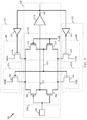
- FIG. 3 is an illustration of a receiver 300 with an amplifier 330 and a modified bias circuit 332.
- the modified bias circuit 332 includes the same circuit 224 that was described earlier in connection with FIG. 2 (bias circuit 224), which provides a means for adjusting the bias current using negative feedback to stabilize the bias voltage 326.
- the modified bias circuit also includes an additional circuit 340 comprising PMOS transistor 318 and NMOS transistor 320, which provides a means for adjusting the bias current using feedback.
- the PMOS transistor 318 is coupled between the positive supply rail V DD and the amplifier 330 and the NMOS transistor 320 is coupled between the amplifier 330 and the negative supply rail V SS .
- the modified bias circuit 332 also includes two inverters 322 and 324, which are used to feed back the output from the amplifier 330 to the gates of transistors 318 and 320, respectively.
- the modified bias circuit 332 uses feedback from the amplifier 330 to provide additional bias current.
- the additional bias current may enable the receiver 300 to perform better in a low power mode.
- an operating voltage of 1.1 V would result in a bias voltage 326 applied to the gates of the PMOS and NMOS transistors 308, 310 of approximately 550 mV. This is less than the threshold voltage V T of both transistors, resulting in very little bias current to the amplifier 330.
- the single-ended output 342 from the amplifier 330 is high, the PMOS transistor 318 is turned on and the NMOS transistor 320 is off.
- the gate-to-source voltage V GS of the PMOS transistor 318 is V DD (for example, 1.1 V), which is much larger than the threshold voltage V T of the transistor 318, the transistor 318 is completely on, adding more bias current from the positive supply rail.
- the negative feedback of the amplifier 330 automatically increases the gate voltage at the input to the NMOS transistor 310.
- the transistor 310 starts to turn on, conducting more current until the current through the transistor 310 is the same as the current through the PMOS transistor 318. It ends at a stable state with both transistors 310 and 318 on and the current through the transistors 310 and 318 being equal.
- the NMOS transistor 320 is turned on and the PMOS transistor 318 is off. Since the V GS of the NMOS transistor 320 is V DD (for example, 1.1V at minimum), which is much larger than threshold voltage V T of the transistor 320, the transistor 320 is completely on, sinking more current through the negative supply rail.
- the negative feedback of amplifier 330 automatically decreases gate voltage of the PMOS transistor 308. With a larger gate-to-source voltage V GS , the PMOS transistor 308 starts to turn on, conducting more current until current through the transistor 308 is the same as current through the NMOS transistor 320.
- a size ratio of transistors 318 and 320 may be less than a size ratio of transistors 308 and 310.
- a size ratio is defined as the size of a first transistor divided by a second transistor.
- a size ratio of transistors 318 and 320 would be the size of transistor 318 divided by the size of transistor 320.
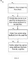
- FIG. 4 is a flow chart 400 illustrating an example of the operation of an amplifier and a bias circuit.
- the bias circuit provides bias current to the amplifier.
- the bias circuit provides a bias current to an amplifier in response to a bias voltage produced by the amplifier.
- the bias circuit may adjust the bias current using negative feedback from the amplifier in response to variations in the bias voltage resulting from PVT variations.
- the bias circuit may adjust the bias current using feedback from the amplifier to add more bias current to allow the receiver to better perform in a low power mode.
- the bias current may be adjusted using feedback from the amplifier and in block 408 the bias current may be further adjusted using additional feedback from the amplifier.
Landscapes
- Engineering & Computer Science (AREA)
- Power Engineering (AREA)
- Amplifiers (AREA)
- Computer Networks & Wireless Communication (AREA)
- Signal Processing (AREA)
- Logic Circuits (AREA)
Applications Claiming Priority (2)
| Application Number | Priority Date | Filing Date | Title |
|---|---|---|---|
| US13/918,771 US9077289B2 (en) | 2013-06-14 | 2013-06-14 | Self-biased receiver |
| PCT/US2014/042259 WO2014201323A1 (en) | 2013-06-14 | 2014-06-13 | Self-biased receiver |
Publications (2)
| Publication Number | Publication Date |
|---|---|
| EP3008820A1 EP3008820A1 (en) | 2016-04-20 |
| EP3008820B1 true EP3008820B1 (en) | 2017-01-04 |
Family
ID=51136831
Family Applications (1)
| Application Number | Title | Priority Date | Filing Date |
|---|---|---|---|
| EP14736560.5A Active EP3008820B1 (en) | 2013-06-14 | 2014-06-13 | Self-biased receiver |
Country Status (6)
Families Citing this family (3)
| Publication number | Priority date | Publication date | Assignee | Title |
|---|---|---|---|---|
| US9935584B1 (en) | 2017-03-30 | 2018-04-03 | Nvidia Corporation | Self-biased gyrator-based receiver for amplification and equalization of single-ended signals |
| CN109831257B (zh) * | 2019-02-13 | 2020-08-11 | 深圳市傲科光电子有限公司 | 一种pam-n cdr电路及其控制方法 |
| US12160204B2 (en) | 2021-02-02 | 2024-12-03 | Macronix International Co., Ltd. | High-speed, low distortion receiver circuit |
Family Cites Families (22)
| Publication number | Priority date | Publication date | Assignee | Title |
|---|---|---|---|---|
| US5293515A (en) | 1989-09-12 | 1994-03-08 | Kabushiki Kaisha Toshiba | Amplifier circuit having two inverters |
| JPH03100996A (ja) * | 1989-09-12 | 1991-04-25 | Toshiba Micro Electron Kk | 増幅回路 |
| US5953276A (en) | 1997-12-18 | 1999-09-14 | Micron Technology, Inc. | Fully-differential amplifier |
| US6118318A (en) | 1997-05-09 | 2000-09-12 | International Business Machines Corporation | Self biased differential amplifier with hysteresis |
| US5942940A (en) | 1997-07-21 | 1999-08-24 | International Business Machines Corporation | Low voltage CMOS differential amplifier |
| KR100327658B1 (ko) | 1998-06-29 | 2002-08-13 | 주식회사 하이닉스반도체 | 데이타입력버퍼 |
| US6169424B1 (en) | 1998-11-03 | 2001-01-02 | Intel Corporation | Self-biasing sense amplifier |
| KR100366616B1 (ko) | 1999-05-19 | 2003-01-09 | 삼성전자 주식회사 | 저전압 인터페이스용 고속 입력버퍼 회로 |
| US6563384B1 (en) | 2000-08-21 | 2003-05-13 | Analog Devices, Inc. | High gain amplifier with rail to rail range and frequency compensation |
| US6392453B1 (en) | 2001-06-20 | 2002-05-21 | Micron Technology, Inc. | Differential input buffer bias circuit |
| US7176720B1 (en) | 2003-03-14 | 2007-02-13 | Cypress Semiconductor Corp. | Low duty cycle distortion differential to CMOS translator |
| JP4346015B2 (ja) * | 2003-06-30 | 2009-10-14 | 株式会社リコー | 高速コンパレータおよびそれを用いたdc/dcコンバータ |
| CN1568035A (zh) * | 2003-07-07 | 2005-01-19 | 深圳市中兴通讯股份有限公司 | 宽带低噪声放大器器件模块装置 |
| KR20060004260A (ko) | 2004-07-09 | 2006-01-12 | 삼성전자주식회사 | 자체 바이어스 차동 증폭기 |
| JP2006332793A (ja) * | 2005-05-23 | 2006-12-07 | Toshiba Microelectronics Corp | 半導体装置 |
| CN100471051C (zh) * | 2007-01-12 | 2009-03-18 | 清华大学 | 一种低电压负反馈跨导放大器 |
| US7683715B2 (en) | 2008-06-27 | 2010-03-23 | Texas Instruments Incorporated | Feedback biasing technique for a stage of an amplifier that uses a feedback control loop having low gain |
| KR101223481B1 (ko) * | 2010-08-30 | 2013-01-17 | 매그나칩 반도체 유한회사 | 오버드라이빙 회로를 포함하는 연산증폭기 |
| TW201210198A (en) * | 2010-08-31 | 2012-03-01 | Novatek Microelectronics Corp | Pre-driver and digital transmitter using the same |
| JP5747532B2 (ja) | 2011-02-01 | 2015-07-15 | 住友電気工業株式会社 | 光受信器 |
| US8519785B2 (en) | 2011-02-15 | 2013-08-27 | Cavium, Inc. | Differential amplifier with duty cycle compensation |
| US8970300B2 (en) * | 2013-04-16 | 2015-03-03 | Texas Instruments Deutschland Gmbh | Apparatus and method for transimpedance amplifiers with wide input current ranges |
-
2013
- 2013-06-14 US US13/918,771 patent/US9077289B2/en active Active
-
2014
- 2014-06-13 EP EP14736560.5A patent/EP3008820B1/en active Active
- 2014-06-13 CN CN201480033689.6A patent/CN105340174B/zh active Active
- 2014-06-13 WO PCT/US2014/042259 patent/WO2014201323A1/en active Application Filing
- 2014-06-13 KR KR1020167000143A patent/KR101762363B1/ko not_active Expired - Fee Related
- 2014-06-13 JP JP2016519669A patent/JP2016526821A/ja active Pending
Also Published As
| Publication number | Publication date |
|---|---|
| US9077289B2 (en) | 2015-07-07 |
| CN105340174A (zh) | 2016-02-17 |
| EP3008820A1 (en) | 2016-04-20 |
| JP2016526821A (ja) | 2016-09-05 |
| KR20160020469A (ko) | 2016-02-23 |
| CN105340174B (zh) | 2017-09-19 |
| US20140368276A1 (en) | 2014-12-18 |
| KR101762363B1 (ko) | 2017-07-27 |
| WO2014201323A1 (en) | 2014-12-18 |
Similar Documents
| Publication | Publication Date | Title |
|---|---|---|
| US20130278296A1 (en) | Multi-Modal Communication Interface | |
| US9124276B2 (en) | Sense amplifier including a level shifter | |
| EP3146622B1 (en) | Feed-forward bias circuit | |
| US8432185B2 (en) | Receiver circuits for differential and single-ended signals | |
| US7576613B2 (en) | Regulated cascode circuits and CMOS analog circuits including the same | |
| US9722585B2 (en) | Circuit and method to extend a signal comparison voltage range | |
| US20140253201A1 (en) | Pulse generation in dual supply systems | |
| KR100718044B1 (ko) | 반도체 장치의 입력회로 | |
| WO2020068230A1 (en) | Transmitter circuitry with n-type pull-up transistor and low output voltage swing | |
| EP3008820B1 (en) | Self-biased receiver | |
| US9294051B2 (en) | Method and apparatus for implementing wide data range and wide common-mode receivers | |
| US10447269B1 (en) | Level shifter | |
| US10742215B1 (en) | Circuit to support multiple voltage level input/output | |
| US20190348958A1 (en) | Low-voltage differential signaling (lvds) receiver circuit and a method of operating the lvds receiver circuit | |
| CN105474535B (zh) | 装置及在装置中的方法 | |
| US7071772B2 (en) | Differential amplifier | |
| US7692455B2 (en) | Semiconductor devices for receiving a current mode signal and methods of operating the same | |
| US20140300386A1 (en) | Voltage level shifter circuit, system, and method for high speed applications | |
| US20240429887A1 (en) | Operational transconductance amplifier with boosted transconductance | |
| US20120062274A1 (en) | Schmitt circuit | |
| US8653859B2 (en) | Electronic comparison circuit | |
| Kim | Design of a low-power CMOS LVDS I/O interface circuit | |
| KR20110040238A (ko) | 수신제어회로 |
Legal Events
| Date | Code | Title | Description |
|---|---|---|---|
| PUAI | Public reference made under article 153(3) epc to a published international application that has entered the european phase |
Free format text: ORIGINAL CODE: 0009012 |
|
| 17P | Request for examination filed |
Effective date: 20160114 |
|
| AK | Designated contracting states |
Kind code of ref document: A1 Designated state(s): AL AT BE BG CH CY CZ DE DK EE ES FI FR GB GR HR HU IE IS IT LI LT LU LV MC MK MT NL NO PL PT RO RS SE SI SK SM TR |
|
| AX | Request for extension of the european patent |
Extension state: BA ME |
|
| REG | Reference to a national code |
Ref country code: DE Ref legal event code: R079 Ref document number: 602014006086 Country of ref document: DE Free format text: PREVIOUS MAIN CLASS: H03F0001300000 Ipc: H03F0003193000 |
|
| RIC1 | Information provided on ipc code assigned before grant |
Ipc: H03F 3/193 20060101AFI20160608BHEP |
|
| GRAP | Despatch of communication of intention to grant a patent |
Free format text: ORIGINAL CODE: EPIDOSNIGR1 |
|
| DAX | Request for extension of the european patent (deleted) | ||
| INTG | Intention to grant announced |
Effective date: 20160718 |
|
| GRAS | Grant fee paid |
Free format text: ORIGINAL CODE: EPIDOSNIGR3 |
|
| GRAA | (expected) grant |
Free format text: ORIGINAL CODE: 0009210 |
|
| AK | Designated contracting states |
Kind code of ref document: B1 Designated state(s): AL AT BE BG CH CY CZ DE DK EE ES FI FR GB GR HR HU IE IS IT LI LT LU LV MC MK MT NL NO PL PT RO RS SE SI SK SM TR |
|
| REG | Reference to a national code |
Ref country code: GB Ref legal event code: FG4D Ref country code: FR Ref legal event code: PLFP Year of fee payment: 4 |
|
| REG | Reference to a national code |
Ref country code: CH Ref legal event code: EP |
|
| REG | Reference to a national code |
Ref country code: AT Ref legal event code: REF Ref document number: 860139 Country of ref document: AT Kind code of ref document: T Effective date: 20170115 |
|
| REG | Reference to a national code |
Ref country code: IE Ref legal event code: FG4D |
|
| REG | Reference to a national code |
Ref country code: DE Ref legal event code: R096 Ref document number: 602014006086 Country of ref document: DE |
|
| REG | Reference to a national code |
Ref country code: LT Ref legal event code: MG4D Ref country code: NL Ref legal event code: MP Effective date: 20170104 |
|
| REG | Reference to a national code |
Ref country code: AT Ref legal event code: MK05 Ref document number: 860139 Country of ref document: AT Kind code of ref document: T Effective date: 20170104 |
|
| PG25 | Lapsed in a contracting state [announced via postgrant information from national office to epo] |
Ref country code: NL Free format text: LAPSE BECAUSE OF FAILURE TO SUBMIT A TRANSLATION OF THE DESCRIPTION OR TO PAY THE FEE WITHIN THE PRESCRIBED TIME-LIMIT Effective date: 20170104 |
|
| PG25 | Lapsed in a contracting state [announced via postgrant information from national office to epo] |
Ref country code: NO Free format text: LAPSE BECAUSE OF FAILURE TO SUBMIT A TRANSLATION OF THE DESCRIPTION OR TO PAY THE FEE WITHIN THE PRESCRIBED TIME-LIMIT Effective date: 20170404 Ref country code: LT Free format text: LAPSE BECAUSE OF FAILURE TO SUBMIT A TRANSLATION OF THE DESCRIPTION OR TO PAY THE FEE WITHIN THE PRESCRIBED TIME-LIMIT Effective date: 20170104 Ref country code: GR Free format text: LAPSE BECAUSE OF FAILURE TO SUBMIT A TRANSLATION OF THE DESCRIPTION OR TO PAY THE FEE WITHIN THE PRESCRIBED TIME-LIMIT Effective date: 20170405 Ref country code: HR Free format text: LAPSE BECAUSE OF FAILURE TO SUBMIT A TRANSLATION OF THE DESCRIPTION OR TO PAY THE FEE WITHIN THE PRESCRIBED TIME-LIMIT Effective date: 20170104 Ref country code: FI Free format text: LAPSE BECAUSE OF FAILURE TO SUBMIT A TRANSLATION OF THE DESCRIPTION OR TO PAY THE FEE WITHIN THE PRESCRIBED TIME-LIMIT Effective date: 20170104 Ref country code: IS Free format text: LAPSE BECAUSE OF FAILURE TO SUBMIT A TRANSLATION OF THE DESCRIPTION OR TO PAY THE FEE WITHIN THE PRESCRIBED TIME-LIMIT Effective date: 20170504 |
|
| PG25 | Lapsed in a contracting state [announced via postgrant information from national office to epo] |
Ref country code: PT Free format text: LAPSE BECAUSE OF FAILURE TO SUBMIT A TRANSLATION OF THE DESCRIPTION OR TO PAY THE FEE WITHIN THE PRESCRIBED TIME-LIMIT Effective date: 20170504 Ref country code: ES Free format text: LAPSE BECAUSE OF FAILURE TO SUBMIT A TRANSLATION OF THE DESCRIPTION OR TO PAY THE FEE WITHIN THE PRESCRIBED TIME-LIMIT Effective date: 20170104 Ref country code: AT Free format text: LAPSE BECAUSE OF FAILURE TO SUBMIT A TRANSLATION OF THE DESCRIPTION OR TO PAY THE FEE WITHIN THE PRESCRIBED TIME-LIMIT Effective date: 20170104 Ref country code: BG Free format text: LAPSE BECAUSE OF FAILURE TO SUBMIT A TRANSLATION OF THE DESCRIPTION OR TO PAY THE FEE WITHIN THE PRESCRIBED TIME-LIMIT Effective date: 20170404 Ref country code: SE Free format text: LAPSE BECAUSE OF FAILURE TO SUBMIT A TRANSLATION OF THE DESCRIPTION OR TO PAY THE FEE WITHIN THE PRESCRIBED TIME-LIMIT Effective date: 20170104 Ref country code: RS Free format text: LAPSE BECAUSE OF FAILURE TO SUBMIT A TRANSLATION OF THE DESCRIPTION OR TO PAY THE FEE WITHIN THE PRESCRIBED TIME-LIMIT Effective date: 20170104 Ref country code: PL Free format text: LAPSE BECAUSE OF FAILURE TO SUBMIT A TRANSLATION OF THE DESCRIPTION OR TO PAY THE FEE WITHIN THE PRESCRIBED TIME-LIMIT Effective date: 20170104 Ref country code: LV Free format text: LAPSE BECAUSE OF FAILURE TO SUBMIT A TRANSLATION OF THE DESCRIPTION OR TO PAY THE FEE WITHIN THE PRESCRIBED TIME-LIMIT Effective date: 20170104 |
|
| REG | Reference to a national code |
Ref country code: DE Ref legal event code: R097 Ref document number: 602014006086 Country of ref document: DE |
|
| PG25 | Lapsed in a contracting state [announced via postgrant information from national office to epo] |
Ref country code: RO Free format text: LAPSE BECAUSE OF FAILURE TO SUBMIT A TRANSLATION OF THE DESCRIPTION OR TO PAY THE FEE WITHIN THE PRESCRIBED TIME-LIMIT Effective date: 20170104 Ref country code: CZ Free format text: LAPSE BECAUSE OF FAILURE TO SUBMIT A TRANSLATION OF THE DESCRIPTION OR TO PAY THE FEE WITHIN THE PRESCRIBED TIME-LIMIT Effective date: 20170104 Ref country code: EE Free format text: LAPSE BECAUSE OF FAILURE TO SUBMIT A TRANSLATION OF THE DESCRIPTION OR TO PAY THE FEE WITHIN THE PRESCRIBED TIME-LIMIT Effective date: 20170104 Ref country code: IT Free format text: LAPSE BECAUSE OF FAILURE TO SUBMIT A TRANSLATION OF THE DESCRIPTION OR TO PAY THE FEE WITHIN THE PRESCRIBED TIME-LIMIT Effective date: 20170104 Ref country code: SK Free format text: LAPSE BECAUSE OF FAILURE TO SUBMIT A TRANSLATION OF THE DESCRIPTION OR TO PAY THE FEE WITHIN THE PRESCRIBED TIME-LIMIT Effective date: 20170104 |
|
| PLBE | No opposition filed within time limit |
Free format text: ORIGINAL CODE: 0009261 |
|
| STAA | Information on the status of an ep patent application or granted ep patent |
Free format text: STATUS: NO OPPOSITION FILED WITHIN TIME LIMIT |
|
| PG25 | Lapsed in a contracting state [announced via postgrant information from national office to epo] |
Ref country code: SM Free format text: LAPSE BECAUSE OF FAILURE TO SUBMIT A TRANSLATION OF THE DESCRIPTION OR TO PAY THE FEE WITHIN THE PRESCRIBED TIME-LIMIT Effective date: 20170104 Ref country code: DK Free format text: LAPSE BECAUSE OF FAILURE TO SUBMIT A TRANSLATION OF THE DESCRIPTION OR TO PAY THE FEE WITHIN THE PRESCRIBED TIME-LIMIT Effective date: 20170104 |
|
| PG25 | Lapsed in a contracting state [announced via postgrant information from national office to epo] |
Ref country code: MC Free format text: LAPSE BECAUSE OF FAILURE TO SUBMIT A TRANSLATION OF THE DESCRIPTION OR TO PAY THE FEE WITHIN THE PRESCRIBED TIME-LIMIT Effective date: 20170104 |
|
| REG | Reference to a national code |
Ref country code: CH Ref legal event code: PL |
|
| PG25 | Lapsed in a contracting state [announced via postgrant information from national office to epo] |
Ref country code: SI Free format text: LAPSE BECAUSE OF FAILURE TO SUBMIT A TRANSLATION OF THE DESCRIPTION OR TO PAY THE FEE WITHIN THE PRESCRIBED TIME-LIMIT Effective date: 20170104 |
|
| REG | Reference to a national code |
Ref country code: IE Ref legal event code: MM4A |
|
| PG25 | Lapsed in a contracting state [announced via postgrant information from national office to epo] |
Ref country code: LI Free format text: LAPSE BECAUSE OF NON-PAYMENT OF DUE FEES Effective date: 20170630 Ref country code: LU Free format text: LAPSE BECAUSE OF NON-PAYMENT OF DUE FEES Effective date: 20170613 Ref country code: CH Free format text: LAPSE BECAUSE OF NON-PAYMENT OF DUE FEES Effective date: 20170630 Ref country code: IE Free format text: LAPSE BECAUSE OF NON-PAYMENT OF DUE FEES Effective date: 20170613 |
|
| REG | Reference to a national code |
Ref country code: FR Ref legal event code: PLFP Year of fee payment: 5 |
|
| REG | Reference to a national code |
Ref country code: BE Ref legal event code: MM Effective date: 20170630 |
|
| PG25 | Lapsed in a contracting state [announced via postgrant information from national office to epo] |
Ref country code: BE Free format text: LAPSE BECAUSE OF NON-PAYMENT OF DUE FEES Effective date: 20170630 |
|
| PGFP | Annual fee paid to national office [announced via postgrant information from national office to epo] |
Ref country code: FR Payment date: 20180516 Year of fee payment: 5 |
|
| PG25 | Lapsed in a contracting state [announced via postgrant information from national office to epo] |
Ref country code: MT Free format text: LAPSE BECAUSE OF NON-PAYMENT OF DUE FEES Effective date: 20170613 |
|
| PGFP | Annual fee paid to national office [announced via postgrant information from national office to epo] |
Ref country code: GB Payment date: 20180403 Year of fee payment: 5 |
|
| PG25 | Lapsed in a contracting state [announced via postgrant information from national office to epo] |
Ref country code: HU Free format text: LAPSE BECAUSE OF FAILURE TO SUBMIT A TRANSLATION OF THE DESCRIPTION OR TO PAY THE FEE WITHIN THE PRESCRIBED TIME-LIMIT; INVALID AB INITIO Effective date: 20140613 |
|
| PG25 | Lapsed in a contracting state [announced via postgrant information from national office to epo] |
Ref country code: CY Free format text: LAPSE BECAUSE OF FAILURE TO SUBMIT A TRANSLATION OF THE DESCRIPTION OR TO PAY THE FEE WITHIN THE PRESCRIBED TIME-LIMIT Effective date: 20170104 |
|
| PG25 | Lapsed in a contracting state [announced via postgrant information from national office to epo] |
Ref country code: MK Free format text: LAPSE BECAUSE OF FAILURE TO SUBMIT A TRANSLATION OF THE DESCRIPTION OR TO PAY THE FEE WITHIN THE PRESCRIBED TIME-LIMIT Effective date: 20170104 |
|
| GBPC | Gb: european patent ceased through non-payment of renewal fee |
Effective date: 20190613 |
|
| PG25 | Lapsed in a contracting state [announced via postgrant information from national office to epo] |
Ref country code: TR Free format text: LAPSE BECAUSE OF FAILURE TO SUBMIT A TRANSLATION OF THE DESCRIPTION OR TO PAY THE FEE WITHIN THE PRESCRIBED TIME-LIMIT Effective date: 20170104 |
|
| PG25 | Lapsed in a contracting state [announced via postgrant information from national office to epo] |
Ref country code: GB Free format text: LAPSE BECAUSE OF NON-PAYMENT OF DUE FEES Effective date: 20190613 |
|
| PG25 | Lapsed in a contracting state [announced via postgrant information from national office to epo] |
Ref country code: FR Free format text: LAPSE BECAUSE OF NON-PAYMENT OF DUE FEES Effective date: 20190630 |
|
| PG25 | Lapsed in a contracting state [announced via postgrant information from national office to epo] |
Ref country code: AL Free format text: LAPSE BECAUSE OF FAILURE TO SUBMIT A TRANSLATION OF THE DESCRIPTION OR TO PAY THE FEE WITHIN THE PRESCRIBED TIME-LIMIT Effective date: 20170104 |
|
| PGFP | Annual fee paid to national office [announced via postgrant information from national office to epo] |
Ref country code: DE Payment date: 20250509 Year of fee payment: 12 |