EP3003672B1 - Verfahren zur herstellung eines optischen moduls - Google Patents
Verfahren zur herstellung eines optischen moduls Download PDFInfo
- Publication number
- EP3003672B1 EP3003672B1 EP14728951.6A EP14728951A EP3003672B1 EP 3003672 B1 EP3003672 B1 EP 3003672B1 EP 14728951 A EP14728951 A EP 14728951A EP 3003672 B1 EP3003672 B1 EP 3003672B1
- Authority
- EP
- European Patent Office
- Prior art keywords
- film
- chip
- optical
- conductor track
- optical element
- Prior art date
- Legal status (The legal status is an assumption and is not a legal conclusion. Google has not performed a legal analysis and makes no representation as to the accuracy of the status listed.)
- Not-in-force
Links
Images



Classifications
-
- H—ELECTRICITY
- H10—SEMICONDUCTOR DEVICES; ELECTRIC SOLID-STATE DEVICES NOT OTHERWISE PROVIDED FOR
- H10W—GENERIC PACKAGES, INTERCONNECTIONS, CONNECTORS OR OTHER CONSTRUCTIONAL DETAILS OF DEVICES COVERED BY CLASS H10
- H10W70/00—Package substrates; Interposers; Redistribution layers [RDL]
- H10W70/01—Manufacture or treatment
- H10W70/05—Manufacture or treatment of insulating or insulated package substrates, or of interposers, or of redistribution layers
- H10W70/08—Manufacture or treatment of insulating or insulated package substrates, or of interposers, or of redistribution layers by depositing layers on the chip or wafer, e.g. "chip-first" RDLs
- H10W70/09—Manufacture or treatment of insulating or insulated package substrates, or of interposers, or of redistribution layers by depositing layers on the chip or wafer, e.g. "chip-first" RDLs extending onto an encapsulation that laterally surrounds the chip or wafer, e.g. fan-out wafer level package [FOWLP] RDLs
-
- H—ELECTRICITY
- H05—ELECTRIC TECHNIQUES NOT OTHERWISE PROVIDED FOR
- H05K—PRINTED CIRCUITS; CASINGS OR CONSTRUCTIONAL DETAILS OF ELECTRIC APPARATUS; MANUFACTURE OF ASSEMBLAGES OF ELECTRICAL COMPONENTS
- H05K1/00—Printed circuits
- H05K1/02—Details
- H05K1/0274—Optical details, e.g. printed circuits comprising integral optical means
-
- H—ELECTRICITY
- H05—ELECTRIC TECHNIQUES NOT OTHERWISE PROVIDED FOR
- H05K—PRINTED CIRCUITS; CASINGS OR CONSTRUCTIONAL DETAILS OF ELECTRIC APPARATUS; MANUFACTURE OF ASSEMBLAGES OF ELECTRICAL COMPONENTS
- H05K1/00—Printed circuits
- H05K1/02—Details
- H05K1/14—Structural association of two or more printed circuits
- H05K1/144—Stacked arrangements of planar printed circuit boards
-
- H—ELECTRICITY
- H05—ELECTRIC TECHNIQUES NOT OTHERWISE PROVIDED FOR
- H05K—PRINTED CIRCUITS; CASINGS OR CONSTRUCTIONAL DETAILS OF ELECTRIC APPARATUS; MANUFACTURE OF ASSEMBLAGES OF ELECTRICAL COMPONENTS
- H05K1/00—Printed circuits
- H05K1/18—Printed circuits structurally associated with non-printed electric components
- H05K1/182—Printed circuits structurally associated with non-printed electric components associated with components mounted in printed circuit boards [PCB], e.g. insert-mounted components [IMC]
- H05K1/185—Printed circuits structurally associated with non-printed electric components associated with components mounted in printed circuit boards [PCB], e.g. insert-mounted components [IMC] associated with components encapsulated in the insulating substrate of the PCBs; associated with components incorporated in internal layers of multilayer circuit boards
-
- H—ELECTRICITY
- H10—SEMICONDUCTOR DEVICES; ELECTRIC SOLID-STATE DEVICES NOT OTHERWISE PROVIDED FOR
- H10F—INORGANIC SEMICONDUCTOR DEVICES SENSITIVE TO INFRARED RADIATION, LIGHT, ELECTROMAGNETIC RADIATION OF SHORTER WAVELENGTH OR CORPUSCULAR RADIATION
- H10F19/00—Integrated devices, or assemblies of multiple devices, comprising at least one photovoltaic cell covered by group H10F10/00, e.g. photovoltaic modules
- H10F19/80—Encapsulations or containers for integrated devices, or assemblies of multiple devices, having photovoltaic cells
-
- H—ELECTRICITY
- H10—SEMICONDUCTOR DEVICES; ELECTRIC SOLID-STATE DEVICES NOT OTHERWISE PROVIDED FOR
- H10F—INORGANIC SEMICONDUCTOR DEVICES SENSITIVE TO INFRARED RADIATION, LIGHT, ELECTROMAGNETIC RADIATION OF SHORTER WAVELENGTH OR CORPUSCULAR RADIATION
- H10F19/00—Integrated devices, or assemblies of multiple devices, comprising at least one photovoltaic cell covered by group H10F10/00, e.g. photovoltaic modules
- H10F19/90—Structures for connecting between photovoltaic cells, e.g. interconnections or insulating spacers
-
- H—ELECTRICITY
- H10—SEMICONDUCTOR DEVICES; ELECTRIC SOLID-STATE DEVICES NOT OTHERWISE PROVIDED FOR
- H10F—INORGANIC SEMICONDUCTOR DEVICES SENSITIVE TO INFRARED RADIATION, LIGHT, ELECTROMAGNETIC RADIATION OF SHORTER WAVELENGTH OR CORPUSCULAR RADIATION
- H10F71/00—Manufacture or treatment of devices covered by this subclass
- H10F71/138—Manufacture of transparent electrodes, e.g. transparent conductive oxides [TCO] or indium tin oxide [ITO] electrodes
-
- H—ELECTRICITY
- H10—SEMICONDUCTOR DEVICES; ELECTRIC SOLID-STATE DEVICES NOT OTHERWISE PROVIDED FOR
- H10F—INORGANIC SEMICONDUCTOR DEVICES SENSITIVE TO INFRARED RADIATION, LIGHT, ELECTROMAGNETIC RADIATION OF SHORTER WAVELENGTH OR CORPUSCULAR RADIATION
- H10F77/00—Constructional details of devices covered by this subclass
- H10F77/50—Encapsulations or containers
-
- H—ELECTRICITY
- H10—SEMICONDUCTOR DEVICES; ELECTRIC SOLID-STATE DEVICES NOT OTHERWISE PROVIDED FOR
- H10F—INORGANIC SEMICONDUCTOR DEVICES SENSITIVE TO INFRARED RADIATION, LIGHT, ELECTROMAGNETIC RADIATION OF SHORTER WAVELENGTH OR CORPUSCULAR RADIATION
- H10F77/00—Constructional details of devices covered by this subclass
- H10F77/93—Interconnections
- H10F77/933—Interconnections for devices having potential barriers
-
- H—ELECTRICITY
- H10—SEMICONDUCTOR DEVICES; ELECTRIC SOLID-STATE DEVICES NOT OTHERWISE PROVIDED FOR
- H10F—INORGANIC SEMICONDUCTOR DEVICES SENSITIVE TO INFRARED RADIATION, LIGHT, ELECTROMAGNETIC RADIATION OF SHORTER WAVELENGTH OR CORPUSCULAR RADIATION
- H10F77/00—Constructional details of devices covered by this subclass
- H10F77/93—Interconnections
- H10F77/933—Interconnections for devices having potential barriers
- H10F77/935—Interconnections for devices having potential barriers for photovoltaic devices or modules
-
- H—ELECTRICITY
- H10—SEMICONDUCTOR DEVICES; ELECTRIC SOLID-STATE DEVICES NOT OTHERWISE PROVIDED FOR
- H10H—INORGANIC LIGHT-EMITTING SEMICONDUCTOR DEVICES HAVING POTENTIAL BARRIERS
- H10H20/00—Individual inorganic light-emitting semiconductor devices having potential barriers, e.g. light-emitting diodes [LED]
- H10H20/80—Constructional details
- H10H20/85—Packages
- H10H20/852—Encapsulations
- H10H20/854—Encapsulations characterised by their material, e.g. epoxy or silicone resins
-
- H—ELECTRICITY
- H10—SEMICONDUCTOR DEVICES; ELECTRIC SOLID-STATE DEVICES NOT OTHERWISE PROVIDED FOR
- H10H—INORGANIC LIGHT-EMITTING SEMICONDUCTOR DEVICES HAVING POTENTIAL BARRIERS
- H10H20/00—Individual inorganic light-emitting semiconductor devices having potential barriers, e.g. light-emitting diodes [LED]
- H10H20/80—Constructional details
- H10H20/85—Packages
- H10H20/857—Interconnections, e.g. lead-frames, bond wires or solder balls
-
- H—ELECTRICITY
- H10—SEMICONDUCTOR DEVICES; ELECTRIC SOLID-STATE DEVICES NOT OTHERWISE PROVIDED FOR
- H10K—ORGANIC ELECTRIC SOLID-STATE DEVICES
- H10K50/00—Organic light-emitting devices
- H10K50/80—Constructional details
- H10K50/805—Electrodes
-
- H—ELECTRICITY
- H10—SEMICONDUCTOR DEVICES; ELECTRIC SOLID-STATE DEVICES NOT OTHERWISE PROVIDED FOR
- H10K—ORGANIC ELECTRIC SOLID-STATE DEVICES
- H10K71/00—Manufacture or treatment specially adapted for the organic devices covered by this subclass
- H10K71/60—Forming conductive regions or layers, e.g. electrodes
- H10K71/611—Forming conductive regions or layers, e.g. electrodes using printing deposition, e.g. ink jet printing
-
- H—ELECTRICITY
- H05—ELECTRIC TECHNIQUES NOT OTHERWISE PROVIDED FOR
- H05K—PRINTED CIRCUITS; CASINGS OR CONSTRUCTIONAL DETAILS OF ELECTRIC APPARATUS; MANUFACTURE OF ASSEMBLAGES OF ELECTRICAL COMPONENTS
- H05K2201/00—Indexing scheme relating to printed circuits covered by H05K1/00
- H05K2201/01—Dielectrics
- H05K2201/0104—Properties and characteristics in general
- H05K2201/0108—Transparent
-
- H—ELECTRICITY
- H05—ELECTRIC TECHNIQUES NOT OTHERWISE PROVIDED FOR
- H05K—PRINTED CIRCUITS; CASINGS OR CONSTRUCTIONAL DETAILS OF ELECTRIC APPARATUS; MANUFACTURE OF ASSEMBLAGES OF ELECTRICAL COMPONENTS
- H05K2201/00—Indexing scheme relating to printed circuits covered by H05K1/00
- H05K2201/10—Details of components or other objects attached to or integrated in a printed circuit board
- H05K2201/10007—Types of components
- H05K2201/10106—Light emitting diode [LED]
-
- H—ELECTRICITY
- H05—ELECTRIC TECHNIQUES NOT OTHERWISE PROVIDED FOR
- H05K—PRINTED CIRCUITS; CASINGS OR CONSTRUCTIONAL DETAILS OF ELECTRIC APPARATUS; MANUFACTURE OF ASSEMBLAGES OF ELECTRICAL COMPONENTS
- H05K2201/00—Indexing scheme relating to printed circuits covered by H05K1/00
- H05K2201/10—Details of components or other objects attached to or integrated in a printed circuit board
- H05K2201/10007—Types of components
- H05K2201/10121—Optical component, e.g. opto-electronic component
-
- H—ELECTRICITY
- H05—ELECTRIC TECHNIQUES NOT OTHERWISE PROVIDED FOR
- H05K—PRINTED CIRCUITS; CASINGS OR CONSTRUCTIONAL DETAILS OF ELECTRIC APPARATUS; MANUFACTURE OF ASSEMBLAGES OF ELECTRICAL COMPONENTS
- H05K3/00—Apparatus or processes for manufacturing printed circuits
- H05K3/46—Manufacturing multilayer circuits
- H05K3/4644—Manufacturing multilayer circuits by building the multilayer layer by layer, i.e. build-up multilayer circuits
-
- H—ELECTRICITY
- H10—SEMICONDUCTOR DEVICES; ELECTRIC SOLID-STATE DEVICES NOT OTHERWISE PROVIDED FOR
- H10H—INORGANIC LIGHT-EMITTING SEMICONDUCTOR DEVICES HAVING POTENTIAL BARRIERS
- H10H20/00—Individual inorganic light-emitting semiconductor devices having potential barriers, e.g. light-emitting diodes [LED]
- H10H20/01—Manufacture or treatment
- H10H20/036—Manufacture or treatment of packages
-
- H—ELECTRICITY
- H10—SEMICONDUCTOR DEVICES; ELECTRIC SOLID-STATE DEVICES NOT OTHERWISE PROVIDED FOR
- H10H—INORGANIC LIGHT-EMITTING SEMICONDUCTOR DEVICES HAVING POTENTIAL BARRIERS
- H10H20/00—Individual inorganic light-emitting semiconductor devices having potential barriers, e.g. light-emitting diodes [LED]
- H10H20/01—Manufacture or treatment
- H10H20/036—Manufacture or treatment of packages
- H10H20/0362—Manufacture or treatment of packages of encapsulations
-
- H—ELECTRICITY
- H10—SEMICONDUCTOR DEVICES; ELECTRIC SOLID-STATE DEVICES NOT OTHERWISE PROVIDED FOR
- H10H—INORGANIC LIGHT-EMITTING SEMICONDUCTOR DEVICES HAVING POTENTIAL BARRIERS
- H10H20/00—Individual inorganic light-emitting semiconductor devices having potential barriers, e.g. light-emitting diodes [LED]
- H10H20/01—Manufacture or treatment
- H10H20/036—Manufacture or treatment of packages
- H10H20/0364—Manufacture or treatment of packages of interconnections
-
- H—ELECTRICITY
- H10—SEMICONDUCTOR DEVICES; ELECTRIC SOLID-STATE DEVICES NOT OTHERWISE PROVIDED FOR
- H10K—ORGANIC ELECTRIC SOLID-STATE DEVICES
- H10K2102/00—Constructional details relating to the organic devices covered by this subclass
- H10K2102/301—Details of OLEDs
- H10K2102/331—Nanoparticles used in non-emissive layers, e.g. in packaging layer
-
- H—ELECTRICITY
- H10—SEMICONDUCTOR DEVICES; ELECTRIC SOLID-STATE DEVICES NOT OTHERWISE PROVIDED FOR
- H10K—ORGANIC ELECTRIC SOLID-STATE DEVICES
- H10K50/00—Organic light-emitting devices
- H10K50/80—Constructional details
- H10K50/84—Passivation; Containers; Encapsulations
- H10K50/841—Self-supporting sealing arrangements
-
- Y—GENERAL TAGGING OF NEW TECHNOLOGICAL DEVELOPMENTS; GENERAL TAGGING OF CROSS-SECTIONAL TECHNOLOGIES SPANNING OVER SEVERAL SECTIONS OF THE IPC; TECHNICAL SUBJECTS COVERED BY FORMER USPC CROSS-REFERENCE ART COLLECTIONS [XRACs] AND DIGESTS
- Y02—TECHNOLOGIES OR APPLICATIONS FOR MITIGATION OR ADAPTATION AGAINST CLIMATE CHANGE
- Y02E—REDUCTION OF GREENHOUSE GAS [GHG] EMISSIONS, RELATED TO ENERGY GENERATION, TRANSMISSION OR DISTRIBUTION
- Y02E10/00—Energy generation through renewable energy sources
- Y02E10/50—Photovoltaic [PV] energy
-
- Y—GENERAL TAGGING OF NEW TECHNOLOGICAL DEVELOPMENTS; GENERAL TAGGING OF CROSS-SECTIONAL TECHNOLOGIES SPANNING OVER SEVERAL SECTIONS OF THE IPC; TECHNICAL SUBJECTS COVERED BY FORMER USPC CROSS-REFERENCE ART COLLECTIONS [XRACs] AND DIGESTS
- Y02—TECHNOLOGIES OR APPLICATIONS FOR MITIGATION OR ADAPTATION AGAINST CLIMATE CHANGE
- Y02E—REDUCTION OF GREENHOUSE GAS [GHG] EMISSIONS, RELATED TO ENERGY GENERATION, TRANSMISSION OR DISTRIBUTION
- Y02E10/00—Energy generation through renewable energy sources
- Y02E10/50—Photovoltaic [PV] energy
- Y02E10/549—Organic PV cells
-
- Y—GENERAL TAGGING OF NEW TECHNOLOGICAL DEVELOPMENTS; GENERAL TAGGING OF CROSS-SECTIONAL TECHNOLOGIES SPANNING OVER SEVERAL SECTIONS OF THE IPC; TECHNICAL SUBJECTS COVERED BY FORMER USPC CROSS-REFERENCE ART COLLECTIONS [XRACs] AND DIGESTS
- Y02—TECHNOLOGIES OR APPLICATIONS FOR MITIGATION OR ADAPTATION AGAINST CLIMATE CHANGE
- Y02P—CLIMATE CHANGE MITIGATION TECHNOLOGIES IN THE PRODUCTION OR PROCESSING OF GOODS
- Y02P70/00—Climate change mitigation technologies in the production process for final industrial or consumer products
- Y02P70/50—Manufacturing or production processes characterised by the final manufactured product
Definitions
- the invention relates to a method for producing an optical module with an integrated into a chip optical element, in particular a light-emitting optical element, such as an LED, EED, HCSELD, OLED or PLED and / or an optical sensor.
- a light-emitting optical element such as an LED, EED, HCSELD, OLED or PLED and / or an optical sensor.
- an electrode structure for LEDs is known in which the electrodes for the wire bonding can be arranged in an edge region.
- the DE 10 2007 004304 A1 describes a thin film light emitting diode chip having a layer stack having a first and an opposing second main radiating surface so that the thin film light emitting diode chip has at least two main radiating directions. Measures are provided both on the first and on the second main emission surface for improving the decoupling of the light generated in the layer sequence.
- the present invention is based on the object to provide an improved method for producing an optical module.
- optical module is understood here to mean a device which serves for illumination purposes or is designed as an optical transmitter or receiver for the purpose of signal transmission.
- the optical module may include one or more optical elements, in particular a matrix optical elements, wherein the optical elements can be radiation sources and / or optical receivers.
- a "chip” is understood here as an integrated circuit, in particular a semiconductor integrated circuit. In such a chip, an optical element can be integrated.
- the production of an optical module is carried out by first providing a chip with at least one integrated optical element.
- the optical element has a first electrode and a second electrode, and the chip has corresponding first and second connection contacts for the electrodes of the integrated optical element.
- the optical element is activated to emit and / or receive radiation depending on the embodiment.
- the optical element has an optically effective side, from which the radiation is emitted or is received via the radiation.
- the first electrode may be transparent or partially transparent to form the optically effective side of the chip.
- an edge of the chip forms the optically effective side of the chip, from which the radiation is radiated, as it is e.g. may be the case with an EED.
- At least one such chip is then connected to a film, so that the film completely covers at least the optically effective side of the chip.
- the connection of the chip with the film can be done for example by gluing, laminating and / or pressing.
- the film is acrylate, polyarylate or polyurethane, wherein the film is transparent at least in the region which is located above the optically active side, for radiation which is emitted or receivable by the optical element when the operating voltage is present.
- the film can be transparent overall or have transparent windows. In the latter case, a transparent window of the film is positioned over the optically effective side of the chip before the connection of the chip with the film, whereupon the connection is then produced, for example, by laminating, gluing or pressing.
- the film is a thin epoxy film.
- a thin and flexible glass sheet is laminated to the film.
- the contacting of at least one of the terminal contacts then takes place via the film by electrically connecting a conductor track arranged on an upper side or rear side of the film to the terminal contact, wherein the conductor track can be applied, for example, by printing to the film.
- Embodiments of the invention are particularly advantageous because the hitherto generally required wire-bonding for the contacting of the electrodes of the optical element due to the use of the film can be omitted.
- the connection of the chip with the film as well as the contacting of the connection contacts can be done inline, for example in a so-called reel-to-reel production.
- connection of the chips with the film is carried out by pressing, so that the film covers the top of the chip and the edge of the chip over the entire surface.
- press-fitting is made possible due to the plastic properties of the film used, namely acrylate, polyarylate or polyurethane.
- Particularly preferred is the use of cold deformable arylate, since then a substantial heating of the chips for the connection with the film is not required.
- a hole is produced in the film, which extends from the upper side of the film to the first connection contact. Subsequently, the contacting of the first connection contact then takes place through the hole.
- This can be done by applying the conductive trace to the foil after the hole has been made by applying conductive ink to the foil, for example by a printing process such as inkjet printing or aerosol jet printing, as well as the hole with the conductive foil Ink is filled so as to connect the terminal contact through the hole with the conductor track.
- Aerosol jet pressure is known per se from the prior art, cf. for example WO 2010/089081 A1 ,
- the hole is made by exposing the film to a laser or plasma, preferably after the chip has been bonded to the film, so that subsequent accurate alignment of the hole in the positioning of the film with respect to the terminal is not required ,
- the optically active side includes the first electrode, which is at least partially transparent.
- the first electrode is formed by intersecting conductor tracks, wherein the first terminal contact is arranged in an edge region of the top side of the chip, in particular in an edge region of the first electrode, or on one edge of the chip in order to minimize the radiation efficiency due to the first connection contact and its Forfeit contact.
- the contacting of the first and, depending on the embodiment, also of the second connection contacts with conductor tracks of the film takes place by flip-chip mounting.
- At least the first connection contact is formed by low-temperature sintering of nanoparticles, which may be applied to the first connection contact and / or the foil.
- a multilayer printed circuit board is first produced, which includes one or more electrical and / or electronic components and an interconnection of these components.
- the multilayer PCB may already include one or more of the chips with the integrated optical element.
- the multilayer PCB is topped off by applying the foil.
- the chip is first connected to the film and contacted and then then the film with the chip is applied to the multilayer PCB to complete this up. For example, this is done by the film is laminated.
- two different multilayer PCBs are produced according to this method, wherein the one or more optical elements in the respective multilayer PCB are used for optical signal transmission with galvanic isolation between the multilayer PCBs.
- the film is a decorative layer, which is particularly advantageous for producing a lighting fixture, for example for integration into a piece of furniture.
- the optical element is a solar cell which is designed for photovoltaic generation of current.
- a solar module is produced for power generation.
- the optical sensor is a sensor for the reception of IR or UV radiation or other radiation in a visible or non-visible wavelength range.
- the optical sensor is designed for wireless energy transmission, in particular for energy transmission by means of electromagnetic waves, in particular for energy transmission by means of a laser.
- the energy transfer takes place by means of electromagnetic waves, in particular in gigahertz or terahertz range, in order to charge an energy store, such as a rechargeable electric battery of an electronic device.
- the electronic device may be, for example, a telecommunications device, such as a smartphone or a tablet computer, or a medical device, in particular for detecting a medical parameter, such as a portable sphygmomanometer.
- the electric battery of the electronic device which serves to supply its energy, can be charged by means of the wireless energy transmission via the optical sensor.
- FIG. 12 shows a cross-sectional view of one embodiment of an optical module 10 including a chip 12 including an on-chip optical element 14, such as an LED.
- the optical element 14 has a first electrode 15, which has a first connection contact 16 of the chip 12, and a second electrode 18 with a second connection contact 20 of the chip 12.
- the first electrode 15 is at least partially transparent, so that radiation can be radiated upward in the direction of arrow 22.
- the first connection contact 16 is located approximately in the center of the first electrode 15.
- the second electrode 18 has a planar and non-transparent design and is connected in a planar manner to the second connection contact 20.
- the optically active side of the chip 12 is formed by the first electrode 15.
- the chip is connected to a foil 24, the foil 24 completely covering the optically effective side of the chip, that is to say here the first electrode 15, as well as the edges 26 of the chip 12.
- the film is a film of acrylate, polyarylate or polyurethane, the polyurethane is unfoamed.
- cold-formable acrylate is used.
- the material of the film is chosen so that it is transparent to radiation that is emitted from the optical element 14 in the direction of arrow 22 when an operating voltage applied to the electrodes 15 and 18.
- the film can overall, be transparent to this radiation or the film may be formed transparent at least above the first electrode 15 to provide there a window for the passage of the radiation.
- the film 24 has on its upper side a conductor track 28 which is electrically connected through a hole 30 in the film to the first connection contact 16.
- the film 22 On its rear side, the film 22 has a further conductor 32, which contacts the second connection contact 20.
- the printed conductor 28 as well as the through-connection through the hole 30 are applied by printing to the upper side of the film 24, whereas the printed conductor 32 is produced by a patterning technique, such as, for example, by coating the backside with copper and a subsequent etching step.
- the conductor 32 may be printed.
- the chip 12 may include an optical sensor to receive an optical signal, for example to trigger a switching operation, or to receive electromagnetic radiation for wireless energy transmission.
- the chip 12 may be a solar cell for generating electrical energy.
- the optical module 10 may form an integral part of a device 8.
- the device 8 may be an electronic device such as a mobile telecommunication device or a mobile battery operated medical device for detecting a biological parameter of a patient.
- the device 8 has a rechargeable battery 9 which is electrically connected to the optical module 10, that is, the chip 12, to recharge it.
- FIGS. 2a to 2d shows the corresponding steps of a manufacturing process.
- the film 24 and the chip 12 are provided. This can be done for example by a reel-to-reel production take place by the film 24 is unwound from a roll and synchronously thereto chips 12 which are secured one behind the other to a band, and of which a chip 12 by way of example in the FIG. 2a is shown, also be handled by a tape.
- the chip 12 is connected to the film 24 by the chip 12 is pressed into the film 24, whereby the film 24 is plastically deformed. This can be done, for example, by passing the film 24 and the strip with the chip 12 past a pressure roller.
- the hole 30 produced in the film 24, for example by the film 20 is applied from above with a laser or a plasma.
- the printed conductors 28 and 32 applied, for example by inkjet printing or by aerosol jet printing, so that the connection contacts 16 and 20 (see FIG. 1 ) are contacted by this.
- FIG. 3 shows a perspective view of an embodiment of an optical module 10, wherein the first electrode 15 is formed by crossing conductor tracks 34.
- the first connection contact 16 is arranged here in an edge region of the electrode 15 and thus also of the chip 12, so that the conductor track 28 extends away from the electrode 15 and practically does not cover it. This is particularly advantageous because it increases the efficiency of the optical element 14.
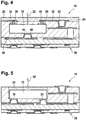
- FIG. 4 shows a sectional view of a multilayer PCB 36, which includes the chip 12 with the optical element 14.
- both terminal contacts 16 and 20 of the optical element 14 on its upper side, that is arranged on the optically effective side.
- These connection contacts 16 and 20 are connected to the corresponding conductor tracks 28 and 32, which are applied in the embodiment considered here on the underside of the film 24, for example by printing by flip-chip contacting, including corresponding Maisierhügel 38 and 40, that is so-called Solder bumps, can be provided.
- the printed conductors 28 and / or 32 of the film 24 may be connected, for example via vias 42, to the underlying circuit structure of the multilayer PCB 36.
- the production of the module 10 can be done here by first the multilayer PCB 36 with the chip 12 and in particular the via 42 is produced. Separately, the conductor tracks 28 and 32 are applied to the film 24, for example by printing technology. Finally, the film 24 provided with the conductor tracks 28 and 32 is applied from above onto the multilayer PCB 36, for example laminated, glued or pressed, so that the contacting mounds 38 and 40 form electrical contacts with the conductor tracks 28 and 32, respectively.
- an operating voltage can be applied to the optical element 14 of the chip 12.
- the chip 12 may have a signal input 44, which is electrically connected, for example, via a via 46 to a conductor track 48 of the multilayer PCB 36. Via this conductor track 48, the chip 12 can receive a switching signal, for example for switching the optical element 14 on and off.
- FIG. 5 shows a further embodiment of the multilayer PCB 36, in which the connection contacts 16 and 20 are arranged on the underside of the chip 12 and the film 24, the top of the chip 12, which forms the optically effective side covers.
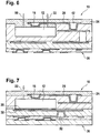
- the FIG. 6 shows a further embodiment of the multilayer PCB 36.
- the terminal contact 16 is arranged centrally on the top of the chip 12.
- the film 24 has on the underside of the conductor track 28, which with the Terminal contact 16 contacted and via the via 42 with the circuit structure of the multilayer PCB 36.
- the production can be carried out so that first the multilayer PCB 36 is made with the chip 12 and then the film 24 is applied to the conductor 28.
- the chip 12 can be designed both to emit an optical signal in the direction of the arrow 22 and to receive an optical signal in the direction of the arrow 50.
- the formation of an electrical connection between the terminal contact 16 and the conductor track 28 and / or between the terminal contact 20 and the conductor track 32 by low-temperature sintering takes place.
- the terminal contact 16 and / or the conductor track 28 nanoparticles, in particular of gold, silver, nickel or copper or of an alloy of these metals.
- the low-temperature sintering for connecting the connection contact 16 to the conductor track 28 can be carried out as "pressureless” low-temperature sintering, "druckfos” being understood here to mean that the low-temperature sintering is not carried out at the high pressures of, for example, 200 bar normally used, but at one much lower pressure, as it is also used for lamination, that is at a pressure of for example 15-20 bar.
- the procedure is such that the film 24 is laminated onto the PCB 36 and at the same time the pressureless low-temperature sintering is carried out in order to connect the connection contact 16 with the conductor track 28.
- FIG. 7 shows one of the FIG. 6 corresponding embodiment, wherein the conductor 32 is realized in the multilayer PCB 36 and not on the film 24.
- the conductor 32 is connected, for example, via a via 52 to further circuit structures of the multilayer PCB.
- This embodiment is particularly advantageous when the film 24 forms the outside of the optical module, and for example has a decor, since the visual appearance can not be affected by running on the surface of the film 24 conductor tracks.
- FIG. 8 shows a further embodiment of the multilayer PCB 36, wherein the terminal contact 16 of the chip 12 is arranged here at the edge of the optically effective side of the chip 12 and the conductor 28 extends away from the optically effective side, so that the conductor 28 has no or only a small has optically covering effect on the optically effective side of the chip 12 - similar to the embodiment according to FIG. 3 ,
- FIG. 9 shows a further embodiment of the PCB 36, in which case the film 24 is transparent only in the upper region 54.
- the production can be carried out here so that first the layers are produced in the lower region 56 of the multilayer PCB 36. Separately, the film 24 is bonded to the chip, for example by press-fitting, and the interconnects for contacting the terminals 16 and 20 of the chip 12 are formed on and in the film, including the via 58, which passes through the film.
- the thus prepared film with the chip 12 and the conductor tracks, in particular the conductor tracks 28 and 32 for contacting the chip 12 is then applied to the top of the area 56 and connected thereto, for example by gluing, laminating or pressing.
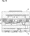
- FIG. 10 shows a further embodiment of the multilayer PCB 36 with an opposing further multilayer PCB 60, which also according to an embodiment of the invention, in particular according to one of FIGS. 4 to 9 can be trained.
- the chip 12 'of the multilayer PCB 60 corresponds to the chip 12 of the multilayer PCB 36 and is designed here as an optical transmitter, whereas the chip 12 is designed as an optical receiver.
- the PCBs 36 and 60 are mechanically but not electrically connected to each other by soldering or bonding dots 62 so that an optical channel for optical signal transmission from the PCB 60 to the PCB 36 is realized over the foils 24 'and 24.
Landscapes
- Engineering & Computer Science (AREA)
- Microelectronics & Electronic Packaging (AREA)
- Physics & Mathematics (AREA)
- Optics & Photonics (AREA)
- Manufacturing & Machinery (AREA)
- Solid State Image Pick-Up Elements (AREA)
- Life Sciences & Earth Sciences (AREA)
- Sustainable Development (AREA)
- Led Device Packages (AREA)
- Sustainable Energy (AREA)
Description
- Die Erfindung betrifft ein Verfahren zur Herstellung eines optischen Moduls mit einem in einen Chip integrierten optischen Element, insbesondere einem lichtemittierenden optischen Element, wie zum Beispiel einer LED, EED, HCSELD, OLED oder PLED und/oder einem optischen Sensor.
- Aus der
DE 10 2007 007 847 A1 ist eine Licht aussendende Vorrichtung und ein Verfahren zu deren Herstellung bekannt. Zur Herstellung der Vorrichtung werden die Anoden- und Kathodenanschlüsse einer LED durch Drahtbonden elektrisch kontaktiert und es wird ein Vergussharz eingesetzt. - Aus der
DE 10 2007 044 446 A1 ist ein flexibler Schaltkreis mit einem Array aus LEDs bekannt. Auch hier werden die LEDs durch Drahtbonding kontaktiert. - Aus der
DE 199 53 160 B4 ist eine Elektrodenstruktur für LEDs bekannt, bei der die Elektroden für das Wire-Bonding in einem Randbereich angeordnet sein können. - Bei LEDs erfolgt die Abstrahlung des Lichts im Allgemeinen durch eine obere transparente Elektrode. Dies muss aber nicht zwangsläufig so sein:
- Aus dem Stand der Technik sind an sich Edge-Emitting Laser Diodes (EELs) bekannt, beispielsweise aus
US 5,105,430 , bei denen das Licht seitlich abgestrahlt wird sowie auch Horizontal-Cavity Surface-Emitting Laser-Dioden (HCSELD), vergleiche Appl. Phys. Lett. 84, 4104 (2004); An InGaN-based horizontal-cavity surface-emitting laser diode. - Aus der zum Anmeldezeitpunkt unveröffentlichten Internationalen Patentanmeldung PCT/EP2012/059476 ist die Kontaktierung eines elektrischen Bauteils mit einer elektrisch leitenden Folie, insbesondere einer Trägerfolie durch Niedertemperatursintern von Nanopartikeln offenbart.
- Die
DE 10 2007 004304 A1 beschreibt einen Dünnfilm-Leuchtdioden-Chip mit einem Schichtenstapel, der eine erste und eine gegenüberliegende zweite Hauptabstrahlfläche aufweist, so dass der Dünnfilm-Leuchtdioden-Chip zumindest zwei Hauptabstrahlrichtungen aufweist. Sowohl auf der ersten als auch auf der zweiten Hauptabstrahlfläche sind Maßnahmen vorgesehen zur Verbesserung der Auskopplung des in der Schichtenfolge erzeugten Lichts. - Der vorliegenden Erfindung liegt demgegenüber die Aufgabe zugrunde, ein verbessertes Verfahren zur Herstellung eines optischen Moduls zu schaffen.
- Die der Erfindung zugrunde liegende Aufgabe wird mit den Merkmalen von Patentanspruch 1 gelöst. Ausführungsformen der Erfindung sind in den abhängigen Patentansprüchen angegeben.
- Unter einem "optischen Modul" wird hier eine Vorrichtung verstanden, die für Beleuchtungszwecke dient oder als optischer Sender oder Empfänger für die Zwecke der Signalübertragung ausgebildet ist. Das optische Modul kann ein oder mehrere optische Elemente, insbesondere auch eine Matrix optische Elemente beinhalten, wobei es sich bei den optischen Elementen um Strahlungsquellen und/oder optische Empfänger handeln kann.
- Unter einem "Chip" wird hier eine integrierte Schaltung verstanden, insbesondere eine integrierte Halbleiterschaltung. In einen solchen Chip kann ein optisches Element integriert sein.
- Nach Ausführungsformen der Erfindung erfolgt die Herstellung eines optischen Moduls, indem zunächst ein Chip mit zumindest einem integrierten optischen Element bereitgestellt wird. Das optische Element hat eine erste Elektrode und eine zweite Elektrode und der Chip hat entsprechende erste und zweite Anschlusskontakte für die Elektroden des integrierten optischen Elements. Durch Anlegen einer Betriebsspannung zwischen diesen Anschlusskontakten wird das optische Element aktiviert, um je nach Ausführungsform Strahlung zu emittieren und/oder zu empfangen. Hierzu hat das optische Element eine optisch wirksame Seite, von der aus die Strahlung emittiert wird bzw. über die Strahlung empfangen wird.
- Je nach Ausführungsform kann beispielsweise die erste Elektrode transparent oder teiltransparent ausgebildet sein, um die optische wirksame Seite des Chips zu bilden. Es ist aber auch möglich, dass eine Kante des Chips die optisch wirksame Seite des Chips bildet, von der aus die Stahlung abgestrahlt wird, wie es z.B. bei einer EED der Fall sein kann.
- Zumindest ein solcher Chip wird dann mit einer Folie verbunden, so dass die Folie zumindest die optisch wirksame Seite des Chips vollständig überdeckt. Die Verbindung des Chips mit der Folie kann beispielsweise durch Kleben, Laminieren und/oder Einpressen erfolgen.
- Bei der Folie handelt es sich um Acrylat, Polyarylat oder Polyurethan, wobei die Folie zumindest in dem Bereich, der sich oberhalb der optisch wirksamen Seite befindet, für Strahlung transparent ist, die von dem optischen Element bei anliegender Betriebsspannung emittierbar oder empfangbar ist. Insbesondere kann die Folie insgesamt transparent sein oder transparente Fenster aufweisen. Im letzteren Fall wird ein transparentes Fenster der Folie vor der Verbindung des Chips mit der Folie über der optisch wirksamen Seite des Chips positioniert woraufhin dann die Verbindung z.B. durch laminieren, kleben oder einpressen hergestellt wird.
- Nach einer Ausführungsform der Erfindung handelt es sich bei der Folie um eine dünne Epoxid-Folie.
- Nach einer Ausführungsform der Erfindung ist auf die Folie eine dünne und flexible Glasfolie laminiert.
- Die Kontaktierung zumindest eines der Anschlusskontakte erfolgt dann über die Folie, indem eine auf einer Oberseite oder Rückseite der Folie angeordnete Leiterbahn mit dem Anschlusskontakt elektrisch verbunden wird, wobei die Leiterbahn beispielsweise drucktechnisch auf die Folie aufgebracht sein kann.
- Ausführungsformen der Erfindung sind besonders vorteilhaft, da das bisher im Allgemeinen erforderliche Wire-Bonding für die Kontaktierung der Elektroden des optischen Elements aufgrund der Verwendung der Folie entfallen kann. Von besonderem weiterem Vorteil ist dabei, dass die Verbindung des Chips mit der Folie sowie die Kontaktierung der Anschlusskontakte inline erfolgen kann, beispielsweise in einer sogenannten Reel-to-Reel-Fertigung.
- Nach einer Ausführungsform der Erfindung erfolgt die Verbindung der Chips mit der Folie durch Einpressen, so dass die Folie die Oberseite des Chips und die Kante des Chips vollflächig überdeckt. Ein solches Einpressen wird aufgrund der plastischen Eigenschaften der verwendeten Folie, nämlich Acrylat, Polyarylat oder Polyurethan, ermöglicht. Besonders bevorzugt ist die Verwendung von kalt verformbaren Arylat, da dann eine wesentliche Erhitzung der Chips für die Verbindung mit der Folie nicht erforderlich ist.
- Nach einer Ausführungsform der Erfindung wird nach der Verbindung des Chips mit der Folie ein Loch in der Folie hergestellt, welches sich von der Oberseite der Folie bis zu dem ersten Anschlusskontakt erstreckt. Anschließend erfolgt dann die Kontaktierung des ersten Anschlusskontakts durch das Loch hindurch. Dies kann dadurch erfolgen, dass nach der Herstellung des Lochs durch Aufbringung von leitfähiger Tinte auf die Folie, zum Beispiel durch ein Druckverfahren, wie Inkjet-Druck oder Aerosol-Jet Druck, die Leiterbahn auf die Folie aufgebracht wird sowie auch das Loch mit der leitfähigen Tinte gefüllt wird, um so den Anschlusskontakt durch das Loch hindurch mit der Leiterbahn zu verbinden. Aerosol-Jet Druck ist an sich aus dem Stand der Technik bekannt, vgl. beispielsweise
WO 2010/089081 A1 . - Nach einer Ausführungsform der Erfindung wird das Loch durch Beaufschlagung der Folie mit einem Laser oder einem Plasma hergestellt, vorzugsweise nachdem der Chip mit der Folie verbunden worden ist, so dass eine nachträgliche genaue Ausrichtung des Lochs bei der Positionierung der Folie bezüglich des Anschlusskontakts nicht erforderlich ist.
- Nach einer Ausführungsform der Erfindung beinhaltet die optisch wirksame Seite die erste Elektrode, die zumindest teilweise transparent ausgebildet ist. Die erste Elektrode wird durch sich kreuzende Leiterbahnen gebildet, wobei der erste Anschlusskontakt in einem Randbereich der Oberseite des Chips, insbesondere in einem Randbereich der ersten Elektrode, oder an einer der Kante des Chips angeordnet ist, um möglichst wenig Strahlungseffizienz aufgrund des ersten Anschlusskontakts und dessen Kontaktierung einzubüßen.
- Nach einer Ausführungsform der Erfindung erfolgt die Kontaktierung der ersten und je nach Ausführungsform auch der zweiten Anschlusskontakte mit Leiterbahnen der Folie durch Flip-Chip-Montage.
- Nach einer Ausführungsform der Erfindung erfolgt die Ausbildung zumindest des ersten Anschlusskontakts durch Niedertemperatursintern von Nanopartikeln, welche auf dem ersten Anschlusskontakt und/oder der Folie aufgebracht sein können. Diese Ausführungsform ist in Kombination mit der Verwendung von kalt verformbarem Acrylat besonders vorteilhaft, da dann insgesamt die Temperaturbeanspruchung der Chips bei der Herstellung minimiert wird.
- Nach einer Ausführungsform der Erfindung wird zunächst ein Multilayer Printed Circuit Board (PCB) hergestellt, das eine oder mehrere elektrische und/oder elektronische Komponenten sowie eine Verschaltung dieser Komponenten beinhaltet. Das Multilayer PCB kann bereits einen oder mehrere der Chips mit dem integrierten optischen Element beinhalten. In diesem Fall wird das Multilayer PCB nach oben abgeschlossen, indem die Folie aufgebracht wird. Alternativ wird der Chip zunächst mit der Folie verbunden und kontaktiert und anschließend wird dann die Folie mit dem Chip auf die Multilayer PCB aufgebracht, um diese nach oben abzuschließen. Beispielsweise erfolgt dies, indem die Folie auflaminiert wird.
- Nach einer Ausführungsform der Erfindung werden nach diesem Verfahren zwei verschiedene Multilayer PCBs hergestellt, wobei das oder die optischen Elemente in der jeweiligen Multilayer PCB für eine optische Signalübertragung mit galvanischer Trennung zwischen den Multilayer PCBs dienen.
- Nach einer Ausführungsform der Erfindung handelt es sich bei der Folie um eine Dekorschicht, was besonders vorteilhaft zur Herstellung eines Beleuchtungskörpers zum Beispiel zur Integration in ein Möbelstück ist.
- Nach einer Ausführungsform der Erfindung handelt es sich bei dem optischen Element um eine Solarzelle, die zur photovoltagen Erzeugung von Strom ausgebildet ist. Nach Ausführungsform der Erfindung wird also ein Solarmodul für die Stromerzeugung hergestellt.
- Nach einer Ausführungsform der Erfindung handelt es sich bei dem optischen Sensor um einen Sensor für den Empfang von IR oder UV-Strahlung oder andere Strahlung in einem sichtbaren oder nicht sichtbaren Wellenlängenbereich.
- Nach einer Ausführungsform der Erfindung ist der optische Sensor für eine drahtlose Energieübertragung ausgebildet, insbesondere für eine Energieübertragung mittels elektromagnetischer Wellen, insbesondere für eine Energieübertragung mittels Laser. Besonders vorzugsweise erfolgt die Energieübertragung mittels elektromagnetischer Wellen, insbesondere in Gigahertz- oder Terrahertzbereich, um einen Energiespeicher, wie zum Beispiel eine aufladbare elektrische Batterie eines elektronischen Geräts, aufzuladen. Bei dem elektronischen Gerät kann es sich zum Beispiel um ein Telekommunikationsgerät, wie zum Beispiel ein Smartphone oder einen Tablet-Computer, oder ein medizintechnisches Gerät insbesondere zur Erfassung eines medizinischen Parameters, wie zum Beispiel ein tragbares Blutdruckmessgerät handeln. Erfindungsgemäß kann die elektrische Batterie des elektronischen Geräts, die zu dessen Energieversorgung dient, mittels der drahtlosen Energieübertragung über den optischen Sensor aufgeladen werden.
- Im Weiteren werden Ausführungsformen der Erfindung mit Bezugnahme auf die Zeichnungen näher erläutert. Es zeigen:
- Fig. 1
- eine Schnittansicht einer ersten Ausführungsform eines optischen Moduls,
- Fig. 2a - 2d
- die Verfahrensschritte einer Ausführungsform eines erfindungsgemäßen Verfahrens zur Herstellung des optischen Moduls gemäß
Fig. 1 , - Fig. 3
- eine perspektivische Ansicht einer Ausführungsform des optischen Moduls mit Anordnung des ersten Anschlusskontakts in einem Randbereich,
- Fig. 4 - Fig. 9
- Schnittansichten verschiedener Ausführungsformen des optischen Moduls als Multilayer PCB,
- Fig. 10
- einer Schnittansicht zweier einander gegenüberliegende erfindungsgemäße PCB mit optischer Kopplung.
- Elemente der nachfolgenden Ausführungsformen, die einander entsprechen oder identisch sind, werden jeweils mit identischen Bezugszeichen gekennzeichnet.
- Die
Figur 1 zeigt eine Schnittansicht einer Ausführungsform eines optischen Moduls 10, welches einen Chip 12 beinhaltet, der ein in dem Chip integriertes optisches Element 14, wie zum Beispiel einer LED beinhaltet. Das optische Element 14 hat eine erste Elektrode 15, die einen ersten Anschlusskontakt 16 des Chips 12 aufweist, sowie eine zweite Elektrode 18 mit einem zweiten Anschlusskontakt 20 des Chips 12. - Bei der hier betrachteten Ausführungsform ist die erste Elektrode 15 zumindest teilweise transparent ausgebildet, so dass Strahlung nach oben in Pfeilrichtung 22 abgestrahlt werden kann. Der erste Anschlusskontakt 16 befindet sich in etwa mittig auf der ersten Elektrode 15. Dagegen ist die zweite Elektrode 18 flächig und nicht transparent ausgebildet und flächig mit dem zweiten Anschlusskontakt 20 verbunden.
- Durch die erste Elektrode 15 wird bei der hier betrachteten Ausführungsform also die optisch wirksame Seite des Chips 12 gebildet.
- Der Chip ist mit einer Folie 24 verbunden, wobei die Folie 24 die optisch wirksame Seite des Chips, das heißt hier die erste Elektrode 15, vollständig überdeckt, sowie auch die Kanten 26 des Chips 12.
- Bei der Folie handelt es sich um eine Folie aus Acrylat, Polyarylat oder Polyurethan, wobei das Polyurethan ungeschäumt ist. Vorzugsweise wird kalt verformbares Acrylat eingesetzt.
- Das Material der Folie ist dabei so gewählt, dass es für Strahlung transparent ist, die von dem optischen Element 14 in der Pfeilrichtung 22 abgegeben wird, wenn eine Betriebsspannung an den Elektroden 15 und 18 anliegt. Dabei kann die Folie insgesamt für diese Strahlung transparent sein oder die Folie kann zumindest oberhalb der ersten Elektrode 15 transparent ausgebildet sein, um dort ein Fenster für den Hindurchtritt der Strahlung zu schaffen.
- Die Folie 24 hat auf ihrer Oberseite eine Leiterbahn 28, welche durch ein Loch 30 in der Folie mit dem ersten Anschlusskontakt 16 elektrisch verbunden ist. Auf ihrer Rückseite hat die Folie 22 eine weitere Leiterbahn 32, welche den zweiten Anschlusskontakt 20 kontaktiert.
- Beispielsweise ist die Leiterbahn 28 sowie auch die Durchkontaktierung durch das Loch 30 drucktechnisch auf die Oberseite der Folie 24 aufgebracht, wohingegen die Leiterbahn 32 durch eine Strukturierungstechnik, wie zum Beispiel durch Beschichtung der Rückseite mit Kupfer und einem anschließenden Ätzschritt hergestellt wird. Alternativ kann auch die Leiterbahn 32 aufgedruckt sein.
- Alternativ oder zusätzlich kann der Chip 12 einen optischen Sensor beinhalten, um ein optisches Signal zum Beispiel zur Auslösung eines Schaltvorgangs zu empfangen oder um elektromagnetische Strahlung für die drahtlose Energieübertragung zu empfangen. Insbesondere kann es sich bei dem Chip 12 um eine Solarzelle für die Erzeugung elektrischer Energie handeln.
- Das optische Modul 10 kann einen integralen Bestandteil einer Vorrichtung 8 bilden. Bei der Vorrichtung 8 kann es sich um ein elektronisches Gerät, wie zum Beispiel ein mobiles Telekommunikationsgerät oder ein mobiles batteriebetriebenes medizintechnisches Gerät zur Erfassung eines biologischen Parameters eines Patienten handeln. Beispielsweise hat die Vorrichtung 8 eine wieder aufladbare Batterie 9, die mit dem optischen Modul 10, das heißt dem Chip 12, elektrisch verbunden ist, um diese wieder aufzuladen.
- Die
Figur 2a bis 2d zeigt die entsprechenden Schritte eines Herstellungsverfahrens. In dem ersten Schritt, der in derFigur 2a dargestellt ist, werden die Folie 24 und der Chip 12 bereitgestellt. Dies kann beispielsweise durch eine Reel-to-Reel-Fertigung erfolgen, indem die Folie 24 von einer Rolle abgewickelt wird und synchron dazu Chips 12, die hintereinander an einem Band befestigt sind, und von denen ein Chip 12 exemplarisch in derFigur 2a gezeigt ist, ebenfalls von einem Band abgewickelt werden. - In dem zweiten Schritt, der in der
Figur 2b dargestellt ist, wird der Chip 12 mit der Folie 24 verbunden, indem der Chip 12 in die Folie 24 eingepresst wird, wodurch die Folie 24 plastisch verformt wird. Dies kann beispielsweise dadurch erfolgen, dass die Folie 24 und das Band mit dem Chip 12 an einer Anpressrolle vorbeigeführt werden. - Anschließend wird dann in dem dritten Schritt, der in der
Figur 2c dargestellt ist, das Loch 30 in der Folie 24 hergestellt, beispielsweise indem die Folie 20 von oben mit einem Laser oder einem Plasma beaufschlagt wird. - Anschließend werden in dem vierten Schritt, der in der
Figur 2d gezeigt ist, die Leiterbahnen 28 und 32 aufgebracht, beispielsweise durch Inkjet-Druck oder durch Aerosol-Jet-Druck, so dass die Anschlusskontakte 16 und 20 (vergleicheFigur 1 ) hierdurch kontaktiert werden. - Die
Figur 3 zeigt eine perspektivische Darstellung einer Ausführungsform eines optischen Moduls 10, wobei die erste Elektrode 15 durch sich kreuzende Leiterbahnen 34 gebildet wird. Der erste Anschlusskontakt 16 ist hier in einem Randbereich der Elektrode 15 und damit auch des Chips 12 angeordnet, so dass die Leiterbahn 28 von der Elektrode 15 weg verläuft und diese praktisch nicht überdeckt. Dies ist besonders vorteilhaft, da dadurch die Effizienz des optischen Elements 14 gesteigert wird. - Die
Figur 4 zeigt eine Schnittansicht einer Multilayer PCB 36, die den Chip 12 mit dem optischen Element 14 beinhaltet. Im Gegensatz zu den Ausführungsformen gemäßFiguren 1 bis 3 sind hier beide Anschlusskontakte 16 und 20 des optischen Elements 14 an dessen Oberseite, d.h. auf der optisch wirksamen Seite, angeordnet. Diese Anschlusskontakte 16 und 20 sind mit den entsprechenden Leiterbahnen 28 und 32, die bei der hier betrachteten Ausführungsform auf der Unterseite der Folie 24 zum Beispiel drucktechnisch aufgebracht sind durch Flip-Chip-Kontaktierung verbunden, wozu entsprechende Kontaktierhügel 38 bzw. 40, das heißt sogenannte Solder Bumps, vorgesehen sein können. - Die Leiterbahnen 28 und/oder 32 der Folie 24 können zum Beispiel über Vias 42 mit der darunter liegenden Schaltungsstruktur der Multilayer PCB 36 verbunden sein.
- Die Herstellung des Moduls 10 kann hier so erfolgen, indem zunächst die Multilayer PCB 36 mit dem Chip 12 und insbesondere dem Via 42 hergestellt wird. Separat davon werden auf die Folie 24 die Leiterbahnen 28 und 32 aufgebracht, beispielsweise drucktechnisch. Schließlich wird die mit den Leiterbahnen 28 und 32 versehene Folie 24 von oben auf die Multilayer PCB 36 aufgebracht, beispielsweise auflaminiert, aufgeklebt oder aufgepresst, so dass die Kontaktierhügel 38 bzw. 40 elektrische Kontakte mit den Leiterbahnen 28 bzw. 32 ausbilden.
- Über die Anschlusskontakte 16 und 20 kann eine Betriebsspannung an das optische Element 14 des Chips 12 angelegt werden. Zusätzlich kann der Chip 12 einen Signaleingang 44 aufweisen, der zum Beispiel über ein Via 46 mit einer Leiterbahn 48 des Multilayer PCB 36 elektrisch verbunden ist. Über diese Leiterbahn 48 kann der Chip 12 ein Schaltsignal beispielsweise zum Ein- und Ausschalten des optischen Elements 14 empfangen.
- Die
Figur 5 zeigt eine weitere Ausführungsform des Multilayer PCB 36, bei der die Anschlusskontakte 16 und 20 an der Unterseite des Chips 12 angeordnet sind und die Folie 24 die Oberseite des Chips 12, welche die optisch wirksame Seite bildet, überdeckt. - Die
Figur 6 zeigt eine weitere Ausführungsform der Multilayer PCB 36. Bei dieser Ausführungsform ist der Anschlusskontakt 16 mittig auf der Oberseite des Chips 12 angeordnet. Die Folie 24 hat an deren Unterseite die Leiterbahn 28, welche mit dem Anschlusskontakt 16 kontaktiert und über das Via 42 mit der Schaltungsstruktur des Multilayer PCB 36. Die Herstellung kann so erfolgen, dass zunächst das Multilayer PCB 36 mit dem Chip 12 hergestellt wird und anschließend die Folie 24 mit der Leiterbahn 28 aufgebracht wird. Der Chip 12 kann hier sowohl zur Abgabe eines optischen Signals in Pfeilrichtung 22 als auch zum Empfang eines optischen Signals in Pfeilrichtung 50 ausgebildet sein. - Nach einer Ausführungsform der Erfindung erfolgt die Ausbildung einer elektrischen Verbindung zwischen dem Anschlusskontakt 16 und der Leiterbahn 28 und/oder zwischen dem Anschlusskontakt 20 und der Leiterbahn 32 durch Niedertemperatursintern.
Hierzu befinden sich beispielsweise auf dem Anschlusskontakt 16 und/oder der Leiterbahn 28 Nanopartikel insbesondere aus Gold, Silber, Nickel oder Kupfer oder aus einer Legierung aus diesen Metallen. Das Niedertemperatursintern zur Verbindung des Anschlusskontakts 16 mit der Leiterbahn 28 kann als "druckloses" Niedertemperatursintern durchgeführt werden, wobei unter "druckfos" hier verstanden wird, dass das Niedertemperatursintern nicht bei den üblicherweise anzuwendenden hohen Drücken von zum Beispiel 200 bar durchgeführt wird, sondern bei einem wesentlich geringeren Druck, wie er auch für das Laminieren verwendet wird, das heißt bei einem Druck von beispielsweise 15-20 bar. - Beispielsweise kann bei der Ausführungsform gemäß
Figur 6 so vorgegangen werden, dass die Folie 24 auf die PCB 36 auflaminiert wird und dabei gleichzeitig das drucklose Niedertemperatursintern durchgeführt wird, um den Anschlusskontakt 16 mit der Leiterbahn 28 zu verbinden. - Die
Figur 7 zeigt eine derFigur 6 entsprechende Ausführungsform, wobei die Leiterbahn 32 in dem Multilayer PCB 36 und nicht auf der Folie 24 realisiert ist. Die Leiterbahn 32 ist zum Beispiel über ein Via 52 mit weiteren Schaltungsstrukturen des Multilayer PCB verbunden. Diese Ausführungsform ist besonders vorteilhaft, wenn die Folie 24 die Außenseite des optischen Moduls bildet, und beispielsweise ein Dekor aufweist, da das optische Erscheinungsbild dann nicht durch auf der Oberfläche der Folie 24 verlaufende Leiterbahnen beeinträchtigt werden kann. - Die
Figur 8 zeigt eine weitere Ausführungsform des Multilayer PCB 36, wobei der Anschlusskontakt 16 des Chips 12 hier am Rand der optisch wirksamen Seite des Chips 12 angeordnet ist und die Leiterbahn 28 weg von der optisch wirksamen Seite verläuft, so dass die Leiterbahn 28 keine oder nur eine geringe optisch abdeckende Wirkung auf die optisch wirksame Seite des Chips 12 hat - ähnlich zu der Ausführungsform gemäßFigur 3 . - Die
Figur 9 zeigt eine weitere Ausführungsform des PCB 36, wobei hier die Folie 24 nur in deren oberen Bereich 54 transparent ist. Die Herstellung kann hier so erfolgen, dass zunächst die Schichten in dem unteren Bereich 56 der Multilayer PCB 36 hergestellt werden. Separat davon wird die Folie 24 mit dem Chip verbunden, beispielsweise durch Einpressen und es werden die Leiterbahnen zur Kontaktierung der Anschlusskontakte 16 und 20 des Chips 12 auf und in der Folie hergestellt, einschließlich des Vias 58, welches hier durch die Folie hindurch verläuft. Die so präparierte Folie mit dem Chip 12 und den Leiterbahnen, insbesondere den Leiterbahnen 28 und 32 zur Kontaktierung des Chips 12, wird dann oben auf den Bereich 56 aufgebracht und mit diesem verbunden, beispielsweise durch Aufkleben, Auflaminieren oder Aufpressen. - Die
Figur 10 zeigt eine weitere Ausführungsform der Multilayer PCB 36 mit einer gegenüberliegenden weiteren Multilayer PCB 60, die ebenfalls nach einer Ausführungsform der Erfindung, insbesondere nach einer derFiguren 4 bis 9 ausgebildet sein kann. Der Chip 12' der Multilayer PCB 60 entspricht dabei dem Chip 12 der Multilayer PCB 36 und ist hier als optischer Sender ausgebildet, wohingegen der Chip 12 als optischer Empfänger ausgebildet ist. Die PCB 36 und 60 sind zum Beispiel durch Löt- oder Klebepunkte 62 miteinander mechanisch, aber nicht galvanisch verbunden, so dass über die Folien 24' und 24 ein optischer Kanal für die optische Signalübertragung von dem PCB 60 an das PCB 36 realisiert ist. -
- 8
- Vorrichtung
- 9
- Batterie
- 10
- Optisches Modul
- 12
- Chip
- 14
- Optisches Element
- 15
- erste Elektrode
- 16
- erster Anschlusskontakt
- 18
- zweite Elektrode
- 20
- zweiter Anschlusskontakt
- 22
- Pfeilrichtung
- 24
- Folie
- 26
- Kante
- 28
- Leiterbahn
- 30
- Loch
- 32
- Leiterbahn
- 34
- Leiterbahn
- 36
- Multilayer PCB
- 38
- Kontaktierhügel
- 40
- Kontaktierhügel
- 42
- Via
- 44
- Signaleingang
- 46
- Via
- 48
- Leiterbahn
- 50
- Pfeilrichtung
- 52
- Via
- 54
- Bereich
- 56
- Bereich
- 58
- Via
- 60
- PCB
Claims (24)
- Verfahren zur Herstellung eines optischen Moduls (10) mit den folgenden Schritten:a) Bereitstellen eines Chips (12) mit einem in den Chip integrierten optischen Element (14), wobei das optische Element eine erste Elektrode (15) und eine zweite Elektrode (18) aufweist, und wobei der Chip einen ersten Anschlusskontakt (16) für die erste Elektrode und einen zweiten Anschlusskontakt (20) für die zweite Elektrode aufweist, so dass zwischen den ersten und zweiten Anschlusskontakten eine Betriebsspannung für das optische Element anlegbar ist, und wobei der Chip eine optisch wirksame Seite (15) hat, welche dazu ausgebildet ist Strahlung zu emittieren und/oder zu empfangen,b) Verbindung des Chips mit einer Folie (24), so dass die Folie die optisch wirksame Seite des Chips vollflächig überdeckt, wobei es sich bei der Folie um eine Folie aus Acrylat, Polyarylat oder Polyurethan handelt, wobei die Folie zumindest in dem Bereich, der sich oberhalb der optisch wirksame Seite befindet, für Strahlung transparent ist, die von dem optischen Element bei anliegender Betriebsspannung emittierbar oder empfangbar ist,c) Kontaktierung des ersten Anschlusskontakts des Chips durch eine auf der Folie angeordnete Leiterbahn (28) und Kontaktierung des zweiten Anschlusskontakts durch eine weitere Leiterbahn (32),
wobei die Verbindung des Chips mit der Folie durch Einpressen des Chips in die Folie erfolgt, so dass die Folie die Oberseite des Chips und die Kanten des Chips vollflächig überdeckt. - Verfahren nach Anspruch 1, wobei es sich bei der Folie um ein kalt verformbares Acrylat handelt.
- Verfahren nach einem der vorhergehenden Ansprüche, wobei sich die optisch wirksame Seite auf der Oberseite des Chips befindet, und sich der erste Anschlusskontakt auf der Oberseite des Chips befindet, wobei nach der Verbindung des Chips mit der Folie ein Loch (30) in der Folie hergestellt wird, welches sich von der Oberseite der Folie bis zu dem ersten Anschlusskontakt erstreckt, und wobei anschließend die Kontaktierung des ersten Anschlusskontakts des Chips mit der auf der Folie angeordneten Leiterbahn (28)durch das Loch hindurch erfolgt.
- Verfahren nach Anspruch 3, wobei das Loch durch Beaufschlagung der Folie mit einem Laser oder einem Plasma hergestellt wird, und/oder wobei die Aufbringung der Leiterbahn auf die Folie und die Kontaktierung der Leiterbahn durch das Loch drucktechnisch erfolgt, und/oder die weitere Leiterbahn (32) drucktechnisch aufgebracht wird, beispielsweise durch Inkjet-Druck oder Aerosol-Jet-Druck.
- Verfahren nach Anspruch 3 oder 4, wobei das Loch durch Beaufschlagung der Folie mit einem Laser oder einem Plasma hergestellt wird.
- Verfahren nach einem der vorhergehenden Ansprüche, wobei die optisch wirksame Seite die erste Elektrode beinhaltet, wobei die erste Elektrode des optischen Elements durch sich kreuzende Leiterbahnen (34) gebildet wird und der erste Anschlusskontakt mit zumindest einer der sich kreuzenden Leiterbahnen verbunden ist, wobei der erste Anschlusskontakt in einem Randbereich der Oberseite des Chips oder an einer der Kanten (26) des Chips angeordnet ist.
- Verfahren nach einem der vorhergehenden Ansprüche, wobei es sich bei dem optischen Element um eine photovoltaische Solarzelle handelt.
- Verfahren nach einem der vorhergehenden Ansprüche, wobei das optische Element eine oder mehrere Leuchtdioden (LED), edge-emitting laser Dioden (EED), horizontal-cavity surface-emitting laser Dioden (HCSELD), organische Leuchtdioden (OLED) oder Polymer-Leuchtdioden (PLED) und/oder einen optischen Sensor beinhaltet.
- Verfahren nach Anspruch 8, wobei es sich bei dem optischen Sensor um einen Sensor für den Empfang mit Strahlung in einem sichtbaren oder unsichtbaren Wellenlängenbereich handelt.
- Verfahren nach einem der Ansprüche 8 oder 9, wobei der optische Sensor zum Empfang von Strahlung für eine drahtlose Energieübertragung ausgebildet ist, und wobei der Sensor mit einem Energiespeicher zum Speicherung der von dem Sensor empfangenen Energie elektrisch verbunden wird.
- Verfahren nach Anspruch 10, wobei es sich bei dem Energiespeicher um eine aufladbare elektrische Batterie (9) handelt, wobei der Sensor dazu ausgebildet ist, die empfangene Energie in elektrische Energie umzuwandeln, um mit der elektrischen Energie die Batterie aufzuladen.
- Verfahren nach einem der vorhergehenden Ansprüche, wobei zumindest einer der ersten Anschlusskontakte einen Kontaktierhügel (38, 40) für eine Flip-Chip-Montage aufweist, um den zumindest einen ersten Anschlusskontakt mittels Flip-Chip-Montage mit der auf der Folie angeordneten Leiterbahn (28, 32) zu kontaktieren.
- Verfahren nach einem der vorhergehenden Ansprüche, wobei Nanopartikel verwendet werden, um die Kontaktierung zumindest des ersten Anschlusskontakts mit der auf der Folie angeordneten Leiterbahn durch Niedertemperatursintern der Nanopartikel herzustellen, wobei die Nanopartikel auf dem ersten Anschlusskontakt und/oder der Folie aufgebracht sind.
- Verfahren nach Anspruch 13, wobei das Niedertemperatursintern als druckloses Niedertemperatursintern durchgeführt wird und die Verbindung des Chips mit der Folie durch Auflaminieren erfolgt, wobei das Auflaminieren gleichzeitig mit dem drucklosen Niedertemperatursintern durchgeführt wird.
- Verfahren nach Anspruch 14, wobei der Druck bei dem drucklosen Niedertemperatursintern zwischen 15 bar und 20 bar beträgt.
- Verfahren nach einem der vorhergehenden Patentansprüche, wobei die Folie mit dem Chip nach unten auf eine Multilayer PCB (36) aufgebracht wird, so dass die auf der Folie angeordnete Leiterbahn mit einer Leiterbahn der Multilayer PCB eine Verbindung ausbildet.
- Verfahren nach Anspruch 16, wobei die Folie auflaminiert wird.
- Verfahren nach Anspruch 16 oder 17, wobei eine weitere Multilayer PCB (60), die nach einem Verfahren gemäß Patentanspruch 10 oder 11 hergestellt worden ist, mit der Multilayer PCB verbunden wird, so dass eine optische Signalübertragung zwischen dem optischen Element der Multilayer PCB und der weiteren Multilayer PCB erfolgen kann.
- Verfahren nach einem der vorhergehenden Ansprüche, wobei es sich bei dem optischen Modul um eine Beleuchtungseinheit, einen optischen Sender und/oder einen optischen Empfänger handelt.
- Verfahren nach einem der vorhergehenden Ansprüche, wobei die ersten und zweiten Anschlusskontakte auf der Oberseite des Chips angeordnet sind.
- Verfahren nach einem der vorhergehenden Ansprüche, wobei es sich bei der Folie um eine Epoxid-Folie handelt.
- Verfahren nach einem der vorhergehenden Ansprüche, wobei auf die Folie eine flexible Glasfolie laminiert ist.
- Verfahren nach einem der vorhergehenden Ansprüche, wobei die Herstellung des optischen Moduls in einer Reel-to-Reel-Fertigung erfolgt.
- Verfahren nach Anspruch 23, wobei der Chip (12) auf einem Band bereitgestellt wird, wobei das Band weitere der Chips (12) trägt, die hintereinander an dem Band befestigt sind, und die Folie (24) auf einer Rolle bereitgestellt wird, wobei die Reel-to-Reel Fertigung so erfolgt, dass die Folie von der Rolle abgewickelt wird und synchron dazu die Chips ebenfalls von deren Band abgewickelt werden, so dass der Chip (12) mit der Folie verbunden wird, indem der Chip in die Folie eingepresst wird, wodurch die Folie plastisch verformt wird, indem die Folie und das Band mit dem Chip (12) an einer Anpressrolle vorbeigeführt werden.
Applications Claiming Priority (2)
| Application Number | Priority Date | Filing Date | Title |
|---|---|---|---|
| DE102013210668.8A DE102013210668A1 (de) | 2013-06-07 | 2013-06-07 | Verfahren zur Herstellung eines optischen Moduls |
| PCT/EP2014/061788 WO2014195444A1 (de) | 2013-06-07 | 2014-06-06 | Verfahren zur herstellung eines optischen moduls |
Publications (2)
| Publication Number | Publication Date |
|---|---|
| EP3003672A1 EP3003672A1 (de) | 2016-04-13 |
| EP3003672B1 true EP3003672B1 (de) | 2017-08-16 |
Family
ID=50897615
Family Applications (1)
| Application Number | Title | Priority Date | Filing Date |
|---|---|---|---|
| EP14728951.6A Not-in-force EP3003672B1 (de) | 2013-06-07 | 2014-06-06 | Verfahren zur herstellung eines optischen moduls |
Country Status (4)
| Country | Link |
|---|---|
| US (1) | US9748514B2 (de) |
| EP (1) | EP3003672B1 (de) |
| DE (1) | DE102013210668A1 (de) |
| WO (1) | WO2014195444A1 (de) |
Families Citing this family (11)
| Publication number | Priority date | Publication date | Assignee | Title |
|---|---|---|---|---|
| DE102015105823A1 (de) * | 2015-04-16 | 2016-10-20 | Osram Oled Gmbh | Optoelektronische Baugruppe und Verfahren zum Herstellen einer optoelektronischen Baugruppe |
| DE102016215577A1 (de) | 2016-08-19 | 2018-02-22 | Bayerische Motoren Werke Aktiengesellschaft | OLED-Leuchtvorrichtung für eine Fahrzeugleuchte |
| JP2018049981A (ja) * | 2016-09-23 | 2018-03-29 | スタンレー電気株式会社 | 半導体発光装置、および、その製造方法 |
| CN110021640B (zh) | 2018-01-08 | 2025-02-11 | 三星显示有限公司 | 电致发光装置 |
| KR102572136B1 (ko) | 2018-01-08 | 2023-08-29 | 삼성디스플레이 주식회사 | 윈도우를 갖는 전계 발광 장치 |
| DE102019104325A1 (de) * | 2019-02-20 | 2020-08-20 | OSRAM Opto Semiconductors Gesellschaft mit beschränkter Haftung | Optoelektronisches Halbleiterbauteil und Herstellungsverfahren für optoelektronische Halbleiterbauteile |
| DE102019120717A1 (de) * | 2019-07-31 | 2021-02-04 | OSRAM Opto Semiconductors Gesellschaft mit beschränkter Haftung | Verfahren zur herstellung eines elektronischen bauelements und elektronisches bauelement |
| KR102953483B1 (ko) | 2020-09-14 | 2026-04-16 | 삼성디스플레이 주식회사 | 표시 장치 |
| KR102955778B1 (ko) | 2020-11-04 | 2026-04-23 | 삼성디스플레이 주식회사 | 기판의 도전성 본딩 구조 및 이를 포함하는 표시 장치 |
| DE102023133714A1 (de) * | 2023-12-01 | 2025-06-05 | Ams-Osram International Gmbh | Herstellen eines substrats für eine leuchtvorrichtung und eine leuchtvorrichtung mit einem solchen substrat |
| DE102025104038A1 (de) * | 2025-02-04 | 2026-08-06 | Ams-Osram International Gmbh | Verfahren zur herstellung eines elektronischen bauelements und elektronisches bauelement |
Family Cites Families (22)
| Publication number | Priority date | Publication date | Assignee | Title |
|---|---|---|---|---|
| US5105430A (en) | 1991-04-09 | 1992-04-14 | The United States Of America As Represented By The United States Department Of Energy | Thin planar package for cooling an array of edge-emitting laser diodes |
| JP3127195B2 (ja) * | 1994-12-06 | 2001-01-22 | シャープ株式会社 | 発光デバイスおよびその製造方法 |
| CN1143394C (zh) * | 1996-08-27 | 2004-03-24 | 精工爱普生株式会社 | 剥离方法、溥膜器件的转移方法和薄膜器件 |
| US5866949A (en) * | 1996-12-02 | 1999-02-02 | Minnesota Mining And Manufacturing Company | Chip scale ball grid array for integrated circuit packaging |
| US6307218B1 (en) | 1998-11-20 | 2001-10-23 | Lumileds Lighting, U.S., Llc | Electrode structures for light emitting devices |
| DE10353679A1 (de) * | 2003-11-17 | 2005-06-02 | Siemens Ag | Kostengünstige, miniaturisierte Aufbau- und Verbindungstechnik für LEDs und andere optoelektronische Module |
| KR101368748B1 (ko) * | 2004-06-04 | 2014-03-05 | 더 보오드 오브 트러스티스 오브 더 유니버시티 오브 일리노이즈 | 인쇄가능한 반도체소자들의 제조 및 조립방법과 장치 |
| DE102005055293A1 (de) * | 2005-08-05 | 2007-02-15 | Osram Opto Semiconductors Gmbh | Verfahren zur Herstellung von Halbleiterchips und Dünnfilm-Halbleiterchip |
| DE102005038642A1 (de) * | 2005-08-12 | 2007-02-15 | Jenoptik Automatisierungstechnik Gmbh | Verpackung mit einer Schwächelinie und Verfahren zur Herstellung derselben |
| JP4820184B2 (ja) | 2006-02-20 | 2011-11-24 | シチズン電子株式会社 | 発光装置とその製造方法 |
| KR101394704B1 (ko) * | 2006-06-30 | 2014-05-16 | 미쓰비시 마테리알 가부시키가이샤 | 태양 전지의 전극 형성용 조성물 및 그 전극의 형성 방법, 그리고 그 형성 방법에 의해 얻어진 전극을 사용한 태양 전지 |
| US20080067526A1 (en) | 2006-09-18 | 2008-03-20 | Tong Fatt Chew | Flexible circuits having improved reliability and thermal dissipation |
| DE102007004304A1 (de) * | 2007-01-29 | 2008-07-31 | Osram Opto Semiconductors Gmbh | Dünnfilm-Leuchtdioden-Chip und Verfahren zur Herstellung eines Dünnfilm-Leuchtdioden-Chips |
| JP5248240B2 (ja) * | 2007-08-30 | 2013-07-31 | 株式会社半導体エネルギー研究所 | 半導体装置 |
| CN101803008B (zh) * | 2007-09-07 | 2012-11-28 | 株式会社半导体能源研究所 | 半导体装置及其制造方法 |
| US7829389B2 (en) * | 2007-10-05 | 2010-11-09 | Texas Instruments Incorporated | Roll-on encapsulation method for semiconductor packages |
| TWI364801B (en) * | 2007-12-20 | 2012-05-21 | Chipmos Technologies Inc | Dice rearrangement package structure using layout process to form a compliant configuration |
| DE102009007800A1 (de) | 2009-02-06 | 2010-08-12 | Fraunhofer-Gesellschaft zur Förderung der angewandten Forschung e.V. | Aerosol-Drucker, dessen Verwendung und Verfahren zur Herstellung von Linienunterbrechungen bei kontinuierlichen Aerosol-Druckverfahren |
| KR101806550B1 (ko) * | 2011-06-14 | 2017-12-07 | 엘지이노텍 주식회사 | 발광소자 패키지 |
| DE102012102847A1 (de) * | 2012-04-02 | 2013-10-02 | Osram Opto Semiconductors Gmbh | Licht emittierendes Halbleiterbauelement und Verfahren zur Herstellung eines Licht emittierenden Halbleiterbauelements |
| US20150131240A1 (en) | 2012-05-22 | 2015-05-14 | Würth Elektronik Gmbh &Co. KG | Method for Producing an Electronic Subassembly |
| US8933473B1 (en) * | 2012-06-01 | 2015-01-13 | Valery Dubin | Method, apparatus and system for providing light source structures on a flexible substrate |
-
2013
- 2013-06-07 DE DE102013210668.8A patent/DE102013210668A1/de not_active Withdrawn
-
2014
- 2014-06-06 WO PCT/EP2014/061788 patent/WO2014195444A1/de not_active Ceased
- 2014-06-06 US US14/896,314 patent/US9748514B2/en not_active Expired - Fee Related
- 2014-06-06 EP EP14728951.6A patent/EP3003672B1/de not_active Not-in-force
Non-Patent Citations (1)
| Title |
|---|
| None * |
Also Published As
| Publication number | Publication date |
|---|---|
| US9748514B2 (en) | 2017-08-29 |
| US20160126491A1 (en) | 2016-05-05 |
| WO2014195444A1 (de) | 2014-12-11 |
| DE102013210668A1 (de) | 2014-12-11 |
| EP3003672A1 (de) | 2016-04-13 |
Similar Documents
| Publication | Publication Date | Title |
|---|---|---|
| WO2014195444A1 (de) | Verfahren zur herstellung eines optischen moduls | |
| TWI390747B (zh) | 使用單石模組組合技術製造的光伏打模組 | |
| US10854582B2 (en) | Light-emitting module | |
| EP2262016B1 (de) | Kostengünstige, miniaturisierte Aufbau- und Verbindungstechnik für LEDs und andere optoelektronische Module | |
| EP2297780B1 (de) | Optoelektronisches modul mit einem trägersubstrat und einer mehrzahl von strahlung emittierenden halbleiterbauelementen und verfahren zu dessen herstellung | |
| DE102009002823A1 (de) | Solarzelle, diese Solarzelle umfassendes Solarmodul sowie Verfahren zu deren Herstellung und zur Herstellung einer Kontaktfolie | |
| EP2923146A1 (de) | Optoelektronische baugruppe und verfahren zum herstellen einer optoelektronischen baugruppe | |
| DE102009060604A1 (de) | Solar-Modul mit einer Leiterplatte und Verfahren zur Herstellung und Anwendung | |
| WO2010000226A1 (de) | Verfahren zur herstellung eines organischen elektronischen bauelements und organisches elektronisches bauelement | |
| WO2010034820A1 (de) | Rfid-transponderantenne | |
| DE102010050342A1 (de) | Laminat mit integriertem elektronischen Bauteil | |
| JP2009302327A (ja) | 配線部材の接続構造およびそれを備えた太陽電池モジュールならびにその製造方法 | |
| DE102010050343A1 (de) | Chipintegrierte Durchkontaktierung von Mehrlagensubstraten | |
| DE102010049333B4 (de) | Verfahren und Vorrichtung zur Herstellung einer bandförmigen Struktur zur Aufnahme von elektronischen Bauteilen | |
| DE102013204326A1 (de) | Solarmodul und Verfahren zur Herstellung eines solchen | |
| EP3262627A1 (de) | Leuchtdiodenvorrichtung und verfahren zum herstellen einer leuchtdiodenvorrichtung | |
| DE102015114645B4 (de) | Chipkarte, vorrichtung und verfahren | |
| WO2011003726A1 (de) | Optoelektronisches bauteil und flachlichtquelle | |
| DE102006021804A1 (de) | Solarzellenmodul sowie Verfahren zur Herstellung von Solarzellenmodulen | |
| DE102011088476A1 (de) | Solarmodul und Verfahren zur Herstellung eines solchen | |
| DE102012007727A1 (de) | Festkörper-Leuchtmittelanordnung sowie Vorrichtung und Verfahren zu deren Herstellung | |
| DE102013205094A1 (de) | Solarmodul und Verfahren zur Herstellung eines solchen | |
| DE102012214216A1 (de) | Organisches Leuchtdiodenmodul und Verfahren zu dessen Herstellung | |
| DE102011077469A1 (de) | Solarzellenmodul und Verfahren zu dessen Herstellung | |
| EP2491582A1 (de) | Verfahren zum herstellen von durchkontaktierungen |
Legal Events
| Date | Code | Title | Description |
|---|---|---|---|
| PUAI | Public reference made under article 153(3) epc to a published international application that has entered the european phase |
Free format text: ORIGINAL CODE: 0009012 |
|
| 17P | Request for examination filed |
Effective date: 20160107 |
|
| AK | Designated contracting states |
Kind code of ref document: A1 Designated state(s): AL AT BE BG CH CY CZ DE DK EE ES FI FR GB GR HR HU IE IS IT LI LT LU LV MC MK MT NL NO PL PT RO RS SE SI SK SM TR |
|
| AX | Request for extension of the european patent |
Extension state: BA ME |
|
| DAX | Request for extension of the european patent (deleted) | ||
| REG | Reference to a national code |
Ref country code: DE Ref legal event code: R079 Ref document number: 502014005075 Country of ref document: DE Free format text: PREVIOUS MAIN CLASS: B29C0043000000 Ipc: H01L0023000000 |
|
| GRAP | Despatch of communication of intention to grant a patent |
Free format text: ORIGINAL CODE: EPIDOSNIGR1 |
|
| RIC1 | Information provided on ipc code assigned before grant |
Ipc: H01L 31/048 20140101ALI20170224BHEP Ipc: H05K 1/14 20060101ALI20170224BHEP Ipc: H01L 51/56 20060101ALI20170224BHEP Ipc: H01L 31/05 20140101ALI20170224BHEP Ipc: H05K 3/46 20060101ALI20170224BHEP Ipc: H01L 31/18 20060101ALI20170224BHEP Ipc: H01L 33/56 20100101ALI20170224BHEP Ipc: H01L 31/02 20060101ALI20170224BHEP Ipc: H01L 23/00 20060101AFI20170224BHEP Ipc: H01L 51/52 20060101ALI20170224BHEP Ipc: H05K 1/18 20060101ALI20170224BHEP Ipc: H01L 31/0203 20140101ALI20170224BHEP Ipc: H01L 51/00 20060101ALI20170224BHEP Ipc: H05K 1/02 20060101ALI20170224BHEP Ipc: H01L 33/62 20100101ALI20170224BHEP |
|
| INTG | Intention to grant announced |
Effective date: 20170403 |
|
| GRAS | Grant fee paid |
Free format text: ORIGINAL CODE: EPIDOSNIGR3 |
|
| GRAA | (expected) grant |
Free format text: ORIGINAL CODE: 0009210 |
|
| AK | Designated contracting states |
Kind code of ref document: B1 Designated state(s): AL AT BE BG CH CY CZ DE DK EE ES FI FR GB GR HR HU IE IS IT LI LT LU LV MC MK MT NL NO PL PT RO RS SE SI SK SM TR |
|
| REG | Reference to a national code |
Ref country code: GB Ref legal event code: FG4D Free format text: NOT ENGLISH |
|
| REG | Reference to a national code |
Ref country code: CH Ref legal event code: EP |
|
| REG | Reference to a national code |
Ref country code: IE Ref legal event code: FG4D Free format text: LANGUAGE OF EP DOCUMENT: GERMAN |
|
| REG | Reference to a national code |
Ref country code: AT Ref legal event code: REF Ref document number: 919848 Country of ref document: AT Kind code of ref document: T Effective date: 20170915 |
|
| REG | Reference to a national code |
Ref country code: DE Ref legal event code: R096 Ref document number: 502014005075 Country of ref document: DE |
|
| REG | Reference to a national code |
Ref country code: NL Ref legal event code: MP Effective date: 20170816 |
|
| REG | Reference to a national code |
Ref country code: LT Ref legal event code: MG4D |
|
| PG25 | Lapsed in a contracting state [announced via postgrant information from national office to epo] |
Ref country code: FI Free format text: LAPSE BECAUSE OF FAILURE TO SUBMIT A TRANSLATION OF THE DESCRIPTION OR TO PAY THE FEE WITHIN THE PRESCRIBED TIME-LIMIT Effective date: 20170816 Ref country code: NL Free format text: LAPSE BECAUSE OF FAILURE TO SUBMIT A TRANSLATION OF THE DESCRIPTION OR TO PAY THE FEE WITHIN THE PRESCRIBED TIME-LIMIT Effective date: 20170816 Ref country code: LT Free format text: LAPSE BECAUSE OF FAILURE TO SUBMIT A TRANSLATION OF THE DESCRIPTION OR TO PAY THE FEE WITHIN THE PRESCRIBED TIME-LIMIT Effective date: 20170816 Ref country code: SE Free format text: LAPSE BECAUSE OF FAILURE TO SUBMIT A TRANSLATION OF THE DESCRIPTION OR TO PAY THE FEE WITHIN THE PRESCRIBED TIME-LIMIT Effective date: 20170816 Ref country code: NO Free format text: LAPSE BECAUSE OF FAILURE TO SUBMIT A TRANSLATION OF THE DESCRIPTION OR TO PAY THE FEE WITHIN THE PRESCRIBED TIME-LIMIT Effective date: 20171116 |
|
| PG25 | Lapsed in a contracting state [announced via postgrant information from national office to epo] |
Ref country code: IS Free format text: LAPSE BECAUSE OF FAILURE TO SUBMIT A TRANSLATION OF THE DESCRIPTION OR TO PAY THE FEE WITHIN THE PRESCRIBED TIME-LIMIT Effective date: 20171216 Ref country code: LV Free format text: LAPSE BECAUSE OF FAILURE TO SUBMIT A TRANSLATION OF THE DESCRIPTION OR TO PAY THE FEE WITHIN THE PRESCRIBED TIME-LIMIT Effective date: 20170816 Ref country code: BG Free format text: LAPSE BECAUSE OF FAILURE TO SUBMIT A TRANSLATION OF THE DESCRIPTION OR TO PAY THE FEE WITHIN THE PRESCRIBED TIME-LIMIT Effective date: 20171116 Ref country code: PL Free format text: LAPSE BECAUSE OF FAILURE TO SUBMIT A TRANSLATION OF THE DESCRIPTION OR TO PAY THE FEE WITHIN THE PRESCRIBED TIME-LIMIT Effective date: 20170816 Ref country code: RS Free format text: LAPSE BECAUSE OF FAILURE TO SUBMIT A TRANSLATION OF THE DESCRIPTION OR TO PAY THE FEE WITHIN THE PRESCRIBED TIME-LIMIT Effective date: 20170816 Ref country code: GR Free format text: LAPSE BECAUSE OF FAILURE TO SUBMIT A TRANSLATION OF THE DESCRIPTION OR TO PAY THE FEE WITHIN THE PRESCRIBED TIME-LIMIT Effective date: 20171117 Ref country code: ES Free format text: LAPSE BECAUSE OF FAILURE TO SUBMIT A TRANSLATION OF THE DESCRIPTION OR TO PAY THE FEE WITHIN THE PRESCRIBED TIME-LIMIT Effective date: 20170816 |
|
| PG25 | Lapsed in a contracting state [announced via postgrant information from national office to epo] |
Ref country code: RO Free format text: LAPSE BECAUSE OF FAILURE TO SUBMIT A TRANSLATION OF THE DESCRIPTION OR TO PAY THE FEE WITHIN THE PRESCRIBED TIME-LIMIT Effective date: 20170816 Ref country code: DK Free format text: LAPSE BECAUSE OF FAILURE TO SUBMIT A TRANSLATION OF THE DESCRIPTION OR TO PAY THE FEE WITHIN THE PRESCRIBED TIME-LIMIT Effective date: 20170816 Ref country code: CZ Free format text: LAPSE BECAUSE OF FAILURE TO SUBMIT A TRANSLATION OF THE DESCRIPTION OR TO PAY THE FEE WITHIN THE PRESCRIBED TIME-LIMIT Effective date: 20170816 |
|
| REG | Reference to a national code |
Ref country code: DE Ref legal event code: R097 Ref document number: 502014005075 Country of ref document: DE |
|
| PG25 | Lapsed in a contracting state [announced via postgrant information from national office to epo] |
Ref country code: IT Free format text: LAPSE BECAUSE OF FAILURE TO SUBMIT A TRANSLATION OF THE DESCRIPTION OR TO PAY THE FEE WITHIN THE PRESCRIBED TIME-LIMIT Effective date: 20170816 Ref country code: SK Free format text: LAPSE BECAUSE OF FAILURE TO SUBMIT A TRANSLATION OF THE DESCRIPTION OR TO PAY THE FEE WITHIN THE PRESCRIBED TIME-LIMIT Effective date: 20170816 Ref country code: EE Free format text: LAPSE BECAUSE OF FAILURE TO SUBMIT A TRANSLATION OF THE DESCRIPTION OR TO PAY THE FEE WITHIN THE PRESCRIBED TIME-LIMIT Effective date: 20170816 Ref country code: SM Free format text: LAPSE BECAUSE OF FAILURE TO SUBMIT A TRANSLATION OF THE DESCRIPTION OR TO PAY THE FEE WITHIN THE PRESCRIBED TIME-LIMIT Effective date: 20170816 |
|
| REG | Reference to a national code |
Ref country code: FR Ref legal event code: PLFP Year of fee payment: 5 |
|
| PLBE | No opposition filed within time limit |
Free format text: ORIGINAL CODE: 0009261 |
|
| STAA | Information on the status of an ep patent application or granted ep patent |
Free format text: STATUS: NO OPPOSITION FILED WITHIN TIME LIMIT |
|
| 26N | No opposition filed |
Effective date: 20180517 |
|
| PG25 | Lapsed in a contracting state [announced via postgrant information from national office to epo] |
Ref country code: SI Free format text: LAPSE BECAUSE OF FAILURE TO SUBMIT A TRANSLATION OF THE DESCRIPTION OR TO PAY THE FEE WITHIN THE PRESCRIBED TIME-LIMIT Effective date: 20170816 |
|
| PG25 | Lapsed in a contracting state [announced via postgrant information from national office to epo] |
Ref country code: MT Free format text: LAPSE BECAUSE OF FAILURE TO SUBMIT A TRANSLATION OF THE DESCRIPTION OR TO PAY THE FEE WITHIN THE PRESCRIBED TIME-LIMIT Effective date: 20170816 |
|
| REG | Reference to a national code |
Ref country code: CH Ref legal event code: PL |
|
| GBPC | Gb: european patent ceased through non-payment of renewal fee |
Effective date: 20180606 |
|
| REG | Reference to a national code |
Ref country code: IE Ref legal event code: MM4A |
|
| PG25 | Lapsed in a contracting state [announced via postgrant information from national office to epo] |
Ref country code: MC Free format text: LAPSE BECAUSE OF FAILURE TO SUBMIT A TRANSLATION OF THE DESCRIPTION OR TO PAY THE FEE WITHIN THE PRESCRIBED TIME-LIMIT Effective date: 20170816 Ref country code: LU Free format text: LAPSE BECAUSE OF NON-PAYMENT OF DUE FEES Effective date: 20180606 |
|
| PG25 | Lapsed in a contracting state [announced via postgrant information from national office to epo] |
Ref country code: GB Free format text: LAPSE BECAUSE OF NON-PAYMENT OF DUE FEES Effective date: 20180606 Ref country code: LI Free format text: LAPSE BECAUSE OF NON-PAYMENT OF DUE FEES Effective date: 20180630 Ref country code: CH Free format text: LAPSE BECAUSE OF NON-PAYMENT OF DUE FEES Effective date: 20180630 Ref country code: IE Free format text: LAPSE BECAUSE OF NON-PAYMENT OF DUE FEES Effective date: 20180606 |
|
| PG25 | Lapsed in a contracting state [announced via postgrant information from national office to epo] |
Ref country code: TR Free format text: LAPSE BECAUSE OF FAILURE TO SUBMIT A TRANSLATION OF THE DESCRIPTION OR TO PAY THE FEE WITHIN THE PRESCRIBED TIME-LIMIT Effective date: 20170816 |
|
| PG25 | Lapsed in a contracting state [announced via postgrant information from national office to epo] |
Ref country code: PT Free format text: LAPSE BECAUSE OF FAILURE TO SUBMIT A TRANSLATION OF THE DESCRIPTION OR TO PAY THE FEE WITHIN THE PRESCRIBED TIME-LIMIT Effective date: 20170816 |
|
| PG25 | Lapsed in a contracting state [announced via postgrant information from national office to epo] |
Ref country code: HU Free format text: LAPSE BECAUSE OF FAILURE TO SUBMIT A TRANSLATION OF THE DESCRIPTION OR TO PAY THE FEE WITHIN THE PRESCRIBED TIME-LIMIT; INVALID AB INITIO Effective date: 20140606 Ref country code: HR Free format text: LAPSE BECAUSE OF FAILURE TO SUBMIT A TRANSLATION OF THE DESCRIPTION OR TO PAY THE FEE WITHIN THE PRESCRIBED TIME-LIMIT Effective date: 20170816 Ref country code: MK Free format text: LAPSE BECAUSE OF NON-PAYMENT OF DUE FEES Effective date: 20170816 Ref country code: CY Free format text: LAPSE BECAUSE OF FAILURE TO SUBMIT A TRANSLATION OF THE DESCRIPTION OR TO PAY THE FEE WITHIN THE PRESCRIBED TIME-LIMIT Effective date: 20170816 |
|
| PG25 | Lapsed in a contracting state [announced via postgrant information from national office to epo] |
Ref country code: AL Free format text: LAPSE BECAUSE OF FAILURE TO SUBMIT A TRANSLATION OF THE DESCRIPTION OR TO PAY THE FEE WITHIN THE PRESCRIBED TIME-LIMIT Effective date: 20170816 |
|
| PGFP | Annual fee paid to national office [announced via postgrant information from national office to epo] |
Ref country code: DE Payment date: 20200618 Year of fee payment: 7 Ref country code: FR Payment date: 20200619 Year of fee payment: 7 |
|
| PGFP | Annual fee paid to national office [announced via postgrant information from national office to epo] |
Ref country code: BE Payment date: 20200625 Year of fee payment: 7 |
|
| PGFP | Annual fee paid to national office [announced via postgrant information from national office to epo] |
Ref country code: AT Payment date: 20200619 Year of fee payment: 7 |
|
| REG | Reference to a national code |
Ref country code: DE Ref legal event code: R119 Ref document number: 502014005075 Country of ref document: DE |
|
| REG | Reference to a national code |
Ref country code: AT Ref legal event code: MM01 Ref document number: 919848 Country of ref document: AT Kind code of ref document: T Effective date: 20210606 |
|
| REG | Reference to a national code |
Ref country code: BE Ref legal event code: MM Effective date: 20210630 |
|
| PG25 | Lapsed in a contracting state [announced via postgrant information from national office to epo] |
Ref country code: DE Free format text: LAPSE BECAUSE OF NON-PAYMENT OF DUE FEES Effective date: 20220101 Ref country code: AT Free format text: LAPSE BECAUSE OF NON-PAYMENT OF DUE FEES Effective date: 20210606 |
|
| PG25 | Lapsed in a contracting state [announced via postgrant information from national office to epo] |
Ref country code: FR Free format text: LAPSE BECAUSE OF NON-PAYMENT OF DUE FEES Effective date: 20210630 |
|
| PG25 | Lapsed in a contracting state [announced via postgrant information from national office to epo] |
Ref country code: BE Free format text: LAPSE BECAUSE OF NON-PAYMENT OF DUE FEES Effective date: 20210630 |