EP3002795A1 - Illumination device - Google Patents
Illumination device Download PDFInfo
- Publication number
- EP3002795A1 EP3002795A1 EP13883832.1A EP13883832A EP3002795A1 EP 3002795 A1 EP3002795 A1 EP 3002795A1 EP 13883832 A EP13883832 A EP 13883832A EP 3002795 A1 EP3002795 A1 EP 3002795A1
- Authority
- EP
- European Patent Office
- Prior art keywords
- wiring
- light emitting
- wall member
- surrounding wall
- board
- Prior art date
- Legal status (The legal status is an assumption and is not a legal conclusion. Google has not performed a legal analysis and makes no representation as to the accuracy of the status listed.)
- Granted
Links
Images




Classifications
-
- H—ELECTRICITY
- H10—SEMICONDUCTOR DEVICES; ELECTRIC SOLID-STATE DEVICES NOT OTHERWISE PROVIDED FOR
- H10H—INORGANIC LIGHT-EMITTING SEMICONDUCTOR DEVICES HAVING POTENTIAL BARRIERS
- H10H20/00—Individual inorganic light-emitting semiconductor devices having potential barriers, e.g. light-emitting diodes [LED]
- H10H20/80—Constructional details
- H10H20/85—Packages
- H10H20/857—Interconnections, e.g. lead-frames, bond wires or solder balls
-
- F—MECHANICAL ENGINEERING; LIGHTING; HEATING; WEAPONS; BLASTING
- F21—LIGHTING
- F21V—FUNCTIONAL FEATURES OR DETAILS OF LIGHTING DEVICES OR SYSTEMS THEREOF; STRUCTURAL COMBINATIONS OF LIGHTING DEVICES WITH OTHER ARTICLES, NOT OTHERWISE PROVIDED FOR
- F21V19/00—Fastening of light sources or lamp holders
- F21V19/001—Fastening of light sources or lamp holders the light sources being semiconductors devices, e.g. LEDs
- F21V19/003—Fastening of light source holders, e.g. of circuit boards or substrates holding light sources
- F21V19/005—Fastening of light source holders, e.g. of circuit boards or substrates holding light sources by permanent fixing means, e.g. gluing, riveting or embedding in a potting compound
-
- F—MECHANICAL ENGINEERING; LIGHTING; HEATING; WEAPONS; BLASTING
- F21—LIGHTING
- F21V—FUNCTIONAL FEATURES OR DETAILS OF LIGHTING DEVICES OR SYSTEMS THEREOF; STRUCTURAL COMBINATIONS OF LIGHTING DEVICES WITH OTHER ARTICLES, NOT OTHERWISE PROVIDED FOR
- F21V23/00—Arrangement of electric circuit elements in or on lighting devices
- F21V23/02—Arrangement of electric circuit elements in or on lighting devices the elements being transformers, impedances or power supply units, e.g. a transformer with a rectifier
-
- F—MECHANICAL ENGINEERING; LIGHTING; HEATING; WEAPONS; BLASTING
- F21—LIGHTING
- F21V—FUNCTIONAL FEATURES OR DETAILS OF LIGHTING DEVICES OR SYSTEMS THEREOF; STRUCTURAL COMBINATIONS OF LIGHTING DEVICES WITH OTHER ARTICLES, NOT OTHERWISE PROVIDED FOR
- F21V23/00—Arrangement of electric circuit elements in or on lighting devices
- F21V23/06—Arrangement of electric circuit elements in or on lighting devices the elements being coupling devices, e.g. connectors
-
- H—ELECTRICITY
- H10—SEMICONDUCTOR DEVICES; ELECTRIC SOLID-STATE DEVICES NOT OTHERWISE PROVIDED FOR
- H10H—INORGANIC LIGHT-EMITTING SEMICONDUCTOR DEVICES HAVING POTENTIAL BARRIERS
- H10H20/00—Individual inorganic light-emitting semiconductor devices having potential barriers, e.g. light-emitting diodes [LED]
- H10H20/80—Constructional details
- H10H20/85—Packages
-
- H—ELECTRICITY
- H10—SEMICONDUCTOR DEVICES; ELECTRIC SOLID-STATE DEVICES NOT OTHERWISE PROVIDED FOR
- H10H—INORGANIC LIGHT-EMITTING SEMICONDUCTOR DEVICES HAVING POTENTIAL BARRIERS
- H10H20/00—Individual inorganic light-emitting semiconductor devices having potential barriers, e.g. light-emitting diodes [LED]
- H10H20/80—Constructional details
- H10H20/85—Packages
- H10H20/8506—Containers
-
- H—ELECTRICITY
- H10—SEMICONDUCTOR DEVICES; ELECTRIC SOLID-STATE DEVICES NOT OTHERWISE PROVIDED FOR
- H10H—INORGANIC LIGHT-EMITTING SEMICONDUCTOR DEVICES HAVING POTENTIAL BARRIERS
- H10H20/00—Individual inorganic light-emitting semiconductor devices having potential barriers, e.g. light-emitting diodes [LED]
- H10H20/80—Constructional details
- H10H20/85—Packages
- H10H20/852—Encapsulations
- H10H20/853—Encapsulations characterised by their shape
-
- H—ELECTRICITY
- H10—SEMICONDUCTOR DEVICES; ELECTRIC SOLID-STATE DEVICES NOT OTHERWISE PROVIDED FOR
- H10W—GENERIC PACKAGES, INTERCONNECTIONS, CONNECTORS OR OTHER CONSTRUCTIONAL DETAILS OF DEVICES COVERED BY CLASS H10
- H10W72/00—Interconnections or connectors in packages
-
- H—ELECTRICITY
- H10—SEMICONDUCTOR DEVICES; ELECTRIC SOLID-STATE DEVICES NOT OTHERWISE PROVIDED FOR
- H10W—GENERIC PACKAGES, INTERCONNECTIONS, CONNECTORS OR OTHER CONSTRUCTIONAL DETAILS OF DEVICES COVERED BY CLASS H10
- H10W90/00—Package configurations
-
- F—MECHANICAL ENGINEERING; LIGHTING; HEATING; WEAPONS; BLASTING
- F21—LIGHTING
- F21V—FUNCTIONAL FEATURES OR DETAILS OF LIGHTING DEVICES OR SYSTEMS THEREOF; STRUCTURAL COMBINATIONS OF LIGHTING DEVICES WITH OTHER ARTICLES, NOT OTHERWISE PROVIDED FOR
- F21V29/00—Protecting lighting devices from thermal damage; Cooling or heating arrangements specially adapted for lighting devices or systems
- F21V29/50—Cooling arrangements
- F21V29/70—Cooling arrangements characterised by passive heat-dissipating elements, e.g. heat-sinks
- F21V29/74—Cooling arrangements characterised by passive heat-dissipating elements, e.g. heat-sinks with fins or blades
- F21V29/76—Cooling arrangements characterised by passive heat-dissipating elements, e.g. heat-sinks with fins or blades with essentially identical parallel planar fins or blades, e.g. with comb-like cross-section
- F21V29/763—Cooling arrangements characterised by passive heat-dissipating elements, e.g. heat-sinks with fins or blades with essentially identical parallel planar fins or blades, e.g. with comb-like cross-section the planes containing the fins or blades having the direction of the light emitting axis
-
- F—MECHANICAL ENGINEERING; LIGHTING; HEATING; WEAPONS; BLASTING
- F21—LIGHTING
- F21Y—INDEXING SCHEME ASSOCIATED WITH SUBCLASSES F21K, F21L, F21S and F21V, RELATING TO THE FORM OR THE KIND OF THE LIGHT SOURCES OR OF THE COLOUR OF THE LIGHT EMITTED
- F21Y2115/00—Light-generating elements of semiconductor light sources
- F21Y2115/10—Light-emitting diodes [LED]
-
- H—ELECTRICITY
- H10—SEMICONDUCTOR DEVICES; ELECTRIC SOLID-STATE DEVICES NOT OTHERWISE PROVIDED FOR
- H10H—INORGANIC LIGHT-EMITTING SEMICONDUCTOR DEVICES HAVING POTENTIAL BARRIERS
- H10H20/00—Individual inorganic light-emitting semiconductor devices having potential barriers, e.g. light-emitting diodes [LED]
- H10H20/80—Constructional details
- H10H20/85—Packages
- H10H20/852—Encapsulations
- H10H20/854—Encapsulations characterised by their material, e.g. epoxy or silicone resins
-
- H—ELECTRICITY
- H10—SEMICONDUCTOR DEVICES; ELECTRIC SOLID-STATE DEVICES NOT OTHERWISE PROVIDED FOR
- H10H—INORGANIC LIGHT-EMITTING SEMICONDUCTOR DEVICES HAVING POTENTIAL BARRIERS
- H10H20/00—Individual inorganic light-emitting semiconductor devices having potential barriers, e.g. light-emitting diodes [LED]
- H10H20/80—Constructional details
- H10H20/85—Packages
- H10H20/855—Optical field-shaping means, e.g. lenses
- H10H20/856—Reflecting means
-
- H—ELECTRICITY
- H10—SEMICONDUCTOR DEVICES; ELECTRIC SOLID-STATE DEVICES NOT OTHERWISE PROVIDED FOR
- H10H—INORGANIC LIGHT-EMITTING SEMICONDUCTOR DEVICES HAVING POTENTIAL BARRIERS
- H10H20/00—Individual inorganic light-emitting semiconductor devices having potential barriers, e.g. light-emitting diodes [LED]
- H10H20/80—Constructional details
- H10H20/85—Packages
- H10H20/858—Means for heat extraction or cooling
- H10H20/8581—Means for heat extraction or cooling characterised by their material
-
- H—ELECTRICITY
- H10—SEMICONDUCTOR DEVICES; ELECTRIC SOLID-STATE DEVICES NOT OTHERWISE PROVIDED FOR
- H10W—GENERIC PACKAGES, INTERCONNECTIONS, CONNECTORS OR OTHER CONSTRUCTIONAL DETAILS OF DEVICES COVERED BY CLASS H10
- H10W72/00—Interconnections or connectors in packages
- H10W72/50—Bond wires
-
- H—ELECTRICITY
- H10—SEMICONDUCTOR DEVICES; ELECTRIC SOLID-STATE DEVICES NOT OTHERWISE PROVIDED FOR
- H10W—GENERIC PACKAGES, INTERCONNECTIONS, CONNECTORS OR OTHER CONSTRUCTIONAL DETAILS OF DEVICES COVERED BY CLASS H10
- H10W72/00—Interconnections or connectors in packages
- H10W72/50—Bond wires
- H10W72/531—Shapes of wire connectors
- H10W72/536—Shapes of wire connectors the connected ends being ball-shaped
-
- H—ELECTRICITY
- H10—SEMICONDUCTOR DEVICES; ELECTRIC SOLID-STATE DEVICES NOT OTHERWISE PROVIDED FOR
- H10W—GENERIC PACKAGES, INTERCONNECTIONS, CONNECTORS OR OTHER CONSTRUCTIONAL DETAILS OF DEVICES COVERED BY CLASS H10
- H10W72/00—Interconnections or connectors in packages
- H10W72/50—Bond wires
- H10W72/531—Shapes of wire connectors
- H10W72/5363—Shapes of wire connectors the connected ends being wedge-shaped
-
- H—ELECTRICITY
- H10—SEMICONDUCTOR DEVICES; ELECTRIC SOLID-STATE DEVICES NOT OTHERWISE PROVIDED FOR
- H10W—GENERIC PACKAGES, INTERCONNECTIONS, CONNECTORS OR OTHER CONSTRUCTIONAL DETAILS OF DEVICES COVERED BY CLASS H10
- H10W72/00—Interconnections or connectors in packages
- H10W72/50—Bond wires
- H10W72/531—Shapes of wire connectors
- H10W72/5366—Shapes of wire connectors the bond wires having kinks
-
- H—ELECTRICITY
- H10—SEMICONDUCTOR DEVICES; ELECTRIC SOLID-STATE DEVICES NOT OTHERWISE PROVIDED FOR
- H10W—GENERIC PACKAGES, INTERCONNECTIONS, CONNECTORS OR OTHER CONSTRUCTIONAL DETAILS OF DEVICES COVERED BY CLASS H10
- H10W72/00—Interconnections or connectors in packages
- H10W72/50—Bond wires
- H10W72/551—Materials of bond wires
- H10W72/552—Materials of bond wires comprising metals or metalloids, e.g. silver
- H10W72/5522—Materials of bond wires comprising metals or metalloids, e.g. silver comprising gold [Au]
-
- H—ELECTRICITY
- H10—SEMICONDUCTOR DEVICES; ELECTRIC SOLID-STATE DEVICES NOT OTHERWISE PROVIDED FOR
- H10W—GENERIC PACKAGES, INTERCONNECTIONS, CONNECTORS OR OTHER CONSTRUCTIONAL DETAILS OF DEVICES COVERED BY CLASS H10
- H10W72/00—Interconnections or connectors in packages
- H10W72/50—Bond wires
- H10W72/551—Materials of bond wires
- H10W72/552—Materials of bond wires comprising metals or metalloids, e.g. silver
- H10W72/5524—Materials of bond wires comprising metals or metalloids, e.g. silver comprising aluminium [Al]
-
- H—ELECTRICITY
- H10—SEMICONDUCTOR DEVICES; ELECTRIC SOLID-STATE DEVICES NOT OTHERWISE PROVIDED FOR
- H10W—GENERIC PACKAGES, INTERCONNECTIONS, CONNECTORS OR OTHER CONSTRUCTIONAL DETAILS OF DEVICES COVERED BY CLASS H10
- H10W72/00—Interconnections or connectors in packages
- H10W72/50—Bond wires
- H10W72/551—Materials of bond wires
- H10W72/552—Materials of bond wires comprising metals or metalloids, e.g. silver
- H10W72/5525—Materials of bond wires comprising metals or metalloids, e.g. silver comprising copper [Cu]
-
- H—ELECTRICITY
- H10—SEMICONDUCTOR DEVICES; ELECTRIC SOLID-STATE DEVICES NOT OTHERWISE PROVIDED FOR
- H10W—GENERIC PACKAGES, INTERCONNECTIONS, CONNECTORS OR OTHER CONSTRUCTIONAL DETAILS OF DEVICES COVERED BY CLASS H10
- H10W72/00—Interconnections or connectors in packages
- H10W72/851—Dispositions of multiple connectors or interconnections
- H10W72/874—On different surfaces
- H10W72/884—Die-attach connectors and bond wires
-
- H—ELECTRICITY
- H10—SEMICONDUCTOR DEVICES; ELECTRIC SOLID-STATE DEVICES NOT OTHERWISE PROVIDED FOR
- H10W—GENERIC PACKAGES, INTERCONNECTIONS, CONNECTORS OR OTHER CONSTRUCTIONAL DETAILS OF DEVICES COVERED BY CLASS H10
- H10W90/00—Package configurations
- H10W90/701—Package configurations characterised by the relative positions of pads or connectors relative to package parts
- H10W90/731—Package configurations characterised by the relative positions of pads or connectors relative to package parts of die-attach connectors
- H10W90/736—Package configurations characterised by the relative positions of pads or connectors relative to package parts of die-attach connectors between a chip and a stacked lead frame, conducting package substrate or heat sink
-
- H—ELECTRICITY
- H10—SEMICONDUCTOR DEVICES; ELECTRIC SOLID-STATE DEVICES NOT OTHERWISE PROVIDED FOR
- H10W—GENERIC PACKAGES, INTERCONNECTIONS, CONNECTORS OR OTHER CONSTRUCTIONAL DETAILS OF DEVICES COVERED BY CLASS H10
- H10W90/00—Package configurations
- H10W90/701—Package configurations characterised by the relative positions of pads or connectors relative to package parts
- H10W90/751—Package configurations characterised by the relative positions of pads or connectors relative to package parts of bond wires
- H10W90/756—Package configurations characterised by the relative positions of pads or connectors relative to package parts of bond wires between a chip and a stacked lead frame, conducting package substrate or heat sink
Definitions
- a height from an upper surface of the light emitting element to an upper end of a loop of the wiring is equal to or less than 160 ⁇ m.
Landscapes
- Engineering & Computer Science (AREA)
- General Engineering & Computer Science (AREA)
- Power Engineering (AREA)
- Led Device Packages (AREA)
- Fastening Of Light Sources Or Lamp Holders (AREA)
- Non-Portable Lighting Devices Or Systems Thereof (AREA)
- Arrangement Of Elements, Cooling, Sealing, Or The Like Of Lighting Devices (AREA)
- Microelectronics & Electronic Packaging (AREA)
Abstract
Description
- Exemplary embodiments hereinafter relate to a lighting system.
- In the related art, there is a lighting system that includes a board, a wiring pattern provided on a surface of the board, plural light emitting diodes (LEDs) provided on the wiring pattern, plural wirings that respectively connect the plural light emitting diodes and the wiring pattern, a surrounding wall member provided on the surface of the board to surround the plural light emitting diodes, and a sealing portion provided inside the surrounding wall member.
- In such a lighting system, thermal deformation (expansion and contraction due to temperature change) occurs in the sealing portion when turning on and turning off the light emitting diodes. Further, when the plural light emitting diodes are used to create a high intensity of light, the size and volume of the sealing portion increase, and the influence due to the thermal deformation increases. Further, in an in-vehicle lighting system, as a large change in an ambient temperature is added thereto (for example, a range of -40°C to +85°C), the influence due to the thermal deformation further increases.
- Further, if the thermal deformation of the sealing portion increases, the wiring that connects the light emitting diodes and the wiring pattern is easily disconnected.
- Thus, it is desirable to provide a lighting system capable of enhancing resistance to temperature change.
- [PTL 1]
JP-A-2013-25935 - An object of the invention is to provide a lighting system capable of enhancing resistance to temperature change.
- According to an aspect of the invention, there is provided a lighting system including: a board; a wiring pattern that is provided on a surface of the board and has a wiring pad; a light emitting element that is provided on the wiring pattern and includes an electrode on a surface thereof opposite to a surface thereof provided on the wiring pattern; a surrounding wall member that is provided to surround the light emitting element; wiring that connects the wiring pad and the electrode; and a sealing portion that is provided inside the surrounding wall member and covers the light emitting element and the wiring. Here, an angle that is formed by a segment that connects a central position of a portion of the board surrounded by the surrounding wall member and a position where the wiring is connected to the wiring pad, and the wiring is 0° to 45°, or 135° to 180°.
- According to the embodiment of the invention, it is possible to provide a lighting system capable of enhancing resistance to temperature change.
-
-
Fig. 1 is a schematic perspective view illustrating alighting system 1 according to an embodiment of the invention. -
Fig. 2 is a schematic perspective exploded view illustrating thelighting system 1 according to the embodiment of the invention. -
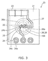
Fig. 3 is a schematic plan view of alight emitting portion 20. -
Fig. 4 is a schematic plan view of alight emitting portion 20 according to another embodiment. -
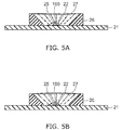
Figs. 5 (a) and 5(b) are schematic sectional views illustrating an influence due to thermal deformation of a sealingportion 27. -
Fig. 6 is a schematic plan view illustrating an arrangement of awiring 25 according to a comparative example. -
Fig. 7 is a schematic perspective view illustrating an end portion of thewiring 25 connected to awiring pad 24c. -
Fig. 8 is a schematic view illustrating an installation angle θ of thewiring 25. -
Fig. 9 is a schematic view illustrating a loop height h of thewiring 25. - According to a first aspect of the invention, a lighting system includes: a board; a wiring pattern that is provided on a surface of the board and has a wiring pad; a light emitting element that is provided on the wiring pattern and includes an electrode on a surface thereof opposite to a surface thereof provided on the wiring pattern; a surrounding wall member that is provided to surround the light emitting element; a wiring that connects the wiring pad and the electrode; and a sealing portion that is provided inside the surrounding wall member and covers the light emitting element and the wiring.
- Here, an angle that is formed by a segment that connects a central position of a portion of the board surrounded by the surrounding wall member and a position where the wiring is connected to the wiring pad, and the wiring is 0° to 45°, or 135° to 180°.
- According to the lighting system, it is possible to enhance resistance to temperature change.
- According to a second aspect of the invention, in the lighting system according to the first aspect of the invention, a linear expansion coefficient of the surrounding wall member is equal to or less than a linear expansion coefficient of the sealing portion.
- According to the lighting system, it is possible to enhance resistance to temperature change.
- According to a third aspect of the invention, in the lighting system according to the first aspect of the invention, a height from an upper surface of the light emitting element to an upper end of a loop of the wiring is equal to or less than 160 µm.
- According to the lighting system, it is possible to enhance resistance to temperature change.
- According to a fourth aspect of the invention, the lighting system according to the first aspect of the invention further includes: a power supply terminal that is electrically connected to the wiring pattern; and a socket that is fitted to the power supply terminal.
- Hereinafter, embodiments will be described with reference to the accompanying drawings. In the respective drawings, the same reference numerals are given to identical components, and detailed description thereof will be appropriately omitted.
-
Fig. 1 and Fig. 2 are schematic perspective views illustrating alighting system 1 according to the present embodiment. -
Fig. 1 is a schematic perspective view of thelighting system 1, andFig. 2 is a schematic perspective exploded view of thelighting system 1. - Further, in
Figs. 1 and 2 , a sealingportion 27 is not shown for ease of understanding. -
Fig. 3 is a schematic plan view of alight emitting portion 20. -
Fig. 4 is a schematic plan view of alight emitting portion 20 according to another embodiment. - In
Fig. 3 andFig. 4 , the number oflight emitting elements 22 and an installation type of awiring 25 are different. - As shown in
Figs. 1 and 2 , thelighting system 1 is provided with amain body portion 10, alight emitting portion 20, apower supply portion 30, and asocket 40. - In the
main body portion 10, anaccommodating portion 11, aflange 12, and afin 13 are provided. - The
accommodating portion 11 has a cylindrical shape and protrudes from one surface of theflange 12. Thelight emitting portion 20 is accommodated inside theaccommodating portion 11. Further, apower supply terminal 31 of thepower supply portion 30 protrudes inside theaccommodating portion 11. - The
flange 12 has a disk shape, in which theaccommodating portion 11 is provided on one surface thereof and thefin 13 is provided on the other surface thereof. - Plural fins 13 protrude from the surface of the
flange 12. Theplural fins 13 have a plate shape and function as radiating fins. - The
main body portion 10 has a function of accommodating thelight emitting portion 20, thepower supply portion 30, and the like, and a function of discharging heat generated by thelight emitting portion 20 and thepower supply portion 30 to the outside of thelighting system 1. - Thus, in consideration of the heat discharge to the outside, it is possible to make the
main body portion 10 of a material with a high thermal conductivity. For example, themain body portion 10 may be formed of aluminum, an aluminum alloy, a resin with a high thermal conductivity, or the like. The resin with the high thermal conductivity is obtained by mixing a resin such as PET or nylon with fibers or particles made of high thermal conductivity carbon, aluminum oxide, or the like, for example. - In this case, a portion that discharges heat to the outside, such as the
fin 13, may be formed of a material with a high thermal conductivity, and the remaining portions may be formed of a resin or the like. - Further, when a main part of the
main body portion 10 is formed of a conductive material, in order to secure electric insulation properties between thepower supply terminal 31 and the conductive material of themain body portion 10, a configuration in which an outer surface of thepower supply terminal 31 is covered with an insulating material (not shown) and a conductive material is disposed thereon may be used. The insulating material is a resin, for example, and preferably, is a material with a high thermal conductivity. Further, a mounting portion capable of being detachably attached to a vehicle lamp tool may be provided in themain body portion 10. - As shown in
Fig. 3 orFig. 4 , aboard 21, alight emitting element 22, acontrol element 23, awiring pattern 24, awiring 25, a surroundingwall member 26, asealing portion 27, and abonding portion 28 are provided in thelight emitting portion 20. - The
board 21 is provided inside theaccommodating portion 11 of themain body portion 10. - The
board 21 has a plate shape, in which thewiring pattern 24 is provided on a surface thereof. - A material used or a structure of the
board 21 is not particularly limited. For example, theboard 21 may be formed of an inorganic material (ceramics) such as aluminum oxide or aluminum nitride, an organic material such as paper phenol or glass epoxy, or the like. Further, theboard 21 may have a configuration in which a surface of a metal plate is coated with an insulator. When the surface of the metal plate is coated with the insulator, the insulator may be formed of an organic material, or may be formed of an inorganic material. - In this case, when a heating value of the
light emitting element 22 is large, it is preferable to form theboard 21 using a material with a high thermal conductivity in terms of heat radiation. As the material with the high thermal conductivity, for example, a material obtained by coating a surface of ceramics such as aluminum oxide or aluminum nitride, a resin with a high thermal conductivity, and a metal plate with an insulator, or the like may be used. - Further, the
board 21 may be a single layer board or a multilayer board. - Plural
light emitting elements 22 are mounted on thewiring pattern 24 provided on a surface of theboard 21. - The
light emitting element 22 may have anelectrode 29 on a surface (upper surface) thereof opposite to a surface thereof provided on the wiring pattern 24 (seeFig. 8 ). Theelectrode 29 may be provided on both the surface (lower surface) provided on thewiring pattern 24 and the surface (upper surface) opposite to the surface provided on thewiring pattern 24, or may be provided only on the surface (upper surface) opposite to the surface provided on thewiring pattern 24. - The
electrode 29 provided on the lower surface of thelight emitting element 22 is electrically connected to amounting pad 24b that is provided in thewiring pattern 24 through a conductive thermosetting material such as silver paste. Theelectrode 29 provided on the upper surface of thelight emitting element 22 is electrically connected to awiring pad 24c that is provided in thewiring pattern 24 through thewiring 25. - The
light emitting element 22 may be a light emitting diode, an organic light emitting diode, a laser diode, or the like. - An upper surface of the
light emitting element 22, which is a light emitting surface, is directed toward a front side of thelighting system 1, and emits light toward the front side of thelighting system 1. - The number, size and the like of the
light emitting elements 22 are not limited to the example shown in the figures, and may be appropriately changed according to the size, usage or the like of thelighting system 1. - The
control element 23 is mounted on thewiring pattern 24. - The
control element 23 controls an electric current flowing in thelight emitting element 22. That is, thecontrol element 23 controls light emission of thelight emitting element 22. - The number, size and the like of the
control elements 23 are not limited to the example shown in the figures, and may be appropriately changed according to the number, type or the like of thelight emitting elements 22. - The
wiring pattern 24 is provided on at least one surface of theboard 21. - The
wiring pattern 24 may be provided on both surfaces of theboard 21, but is preferably provided on one surface of theboard 21 in order to reduce the manufacturing cost. - The
wiring pattern 24 is provided with aninput terminal 24a. -
Plural input terminals 24a are provided. Thepower supply terminal 31 of thepower supply portion 30 is electrically connected to theinput terminal 24a. Thus, thelight emitting element 22 is electrically connected to thepower supply portion 30 through thewiring pattern 24. - The
wiring 25 electrically connects theelectrode 29 provided on the upper surface of thelight emitting element 22 and thewiring pad 24c provided in thewiring pattern 24. - The
wiring 25 may be formed of a cable using gold as a main component, for example. Here, the material of thewiring 25 is not limited to a material using gold as a main component, and may be a material using copper as a main component or a material using aluminum as a main component. - The
wiring 25 electrically connects theelectrode 29 provided on the upper surface of thelight emitting element 22 to thewiring pad 24c provided in thewiring pattern 24 by ultrasonic welding or hot welding. Thewiring 25 may be electrically connected to theelectrode 29 provided on the upper surface of thelight emitting element 22 and thewiring pad 24c provided in thewiring pattern 24 using a wire bonding method, for example. - Further, a circuit component (not shown) or the like may be appropriately provided as necessary. The circuit component (not shown) may be mounted on the
wiring pattern 24, for example. - The surrounding
wall member 26 is provided on theboard 21 to surround the plurallight emitting elements 22. The surroundingwall member 26 has a ring shape, for example, so that the plurallight emitting elements 22 are arranged in acentral portion 26a thereof. - The surrounding
wall member 26 may be formed of a resin such as polybutylene terephthalate (PBT) or polycarbonate (PC), ceramics, or the like. - Further, when the material of the surrounding
wall member 26 is a resin, particles made of titanium oxide or the like may be mixed therein to improve reflectance to light emitted from thelight emitting element 22. - The material of the particles is not limited to titanium oxide, and any material with high reflectance to the light emitted from the
light emitting element 22 may be used for particles to be mixed. - Further, the surrounding
wall member 26 may be formed of a white resin, for example. - A
side wall surface 26b of the surroundingwall member 26 on a side of thecentral portion 26a is formed as an inclined surface. A part of the light emitted from thelight emitting element 22 is reflected from theside wall surface 26b of the surroundingwall member 26, and is emitted toward the front side of thelighting system 1. - Further, light that is a part of the light emitted from the
light emitting element 22 toward the front side of thelighting system 1 and is totally reflected on an upper surface (interface between the sealingportion 27 and the outside air) of the sealingportion 27 is reflected from theside wall surface 26b of the surroundingwall member 26 on the side of thecentral portion 26a, and is emitted again toward the front side of thelighting system 1. - That is, the surrounding
wall member 26 may have a reflector function. The configuration of the surroundingwall member 26 is not limited to the example shown in the figures, and may be appropriately changed. - The sealing
portion 27 is provided in thecentral portion 26a of the surroundingwall member 26. The sealingportion 27 is provided to cover the inside of the surroundingwall member 26. That is, the sealingportion 27 is provided inside the surroundingwall member 26 to cover thelight emitting elements 22 and thewirings 25. - The sealing
portion 27 is formed of a light transmitting material. The sealingportion 27 may be formed of a silicone resin, for example. - The sealing
portion 27 may be formed by filling thecentral portion 26a of the surroundingwall member 26 with a resin, for example. The filling of the resin may be performed using a liquid quantitative discharge apparatus such as a dispenser. - If the
central portion 26a of the surroundingwall member 26 is filled with the resin, it is possible to suppress mechanical contact from the outside with respect to thelight emitting elements 22, thewiring pattern 24 arranged in thecentral portion 26a of the surroundingwall member 26, thewirings 25, or the like. Further, it is possible to suppress air, moisture or the like from being attached to thelight emitting elements 22, thewiring pattern 24 arranged in thecentral portion 26a of the surroundingwall member 26, thewirings 25, or the like. Thus, it is possible to enhance the reliability of thelighting system 1. - Further, the sealing
portion 27 may include a fluorescent substance. The fluorescent substance may be embodied as a YAG type fluorescent substance (yttrium aluminum garnet type fluorescent substance), for example. - For example, when the
light emitting element 22 is a blue light emitting diode and the fluorescent substance is the YAG type fluorescent substance, the YAG type fluorescent substance is excited by blue light emitted from thelight emitting element 22, and yellow fluorescence is emitted from the YAG type fluorescent substance. Further, as the blue light is mixed with the yellow light, white light is emitted from thelighting system 1. The type of the fluorescent substance or the type of thelight emitting element 22 is not limited to an example described above, and may be appropriately changed so that a desired light emitting color is obtained according to the usage or the like of thelighting system 1. - The
bonding portion 28 bonds the surroundingwall member 26 with theboard 21. - The
bonding portion 28 has a film shape, and is provided between the surroundingwall member 26 and theboard 21. - The
bonding portion 28 may be formed by curing a silicone based adhesive or an epoxy based adhesive, for example. - The
bonding portion 28 may be formed through the following procedure, for example. - First, a silicon based adhesive or an epoxy based adhesive is coated in a region on the surface of the
board 21 where the surroundingwall member 26 is provided. - For example, the adhesive is coated in the region on the surface of the
board 21 where the surroundingwall member 26 is provided using a dispenser or the like. - Then, the adhesive is cured by evaporating a solvent or the like to form the
bonding portion 28, and to bond the surroundingwall member 26 with theboard 21. - For example, first, the surrounding
wall member 26 is placed on the coated adhesive. - Subsequently, the surrounding
wall member 26 is pressed to bring the adhesive into close contact with the surroundingwall member 26, and the position (thickness of the adhesive) of the surroundingwall member 26 is adjusted. - Then, the adhesive is cured by evaporating the solvent or the like.
- Here, it is preferable that the viscosity of the adhesive before curing is 1 Pa·s to 15 Pa·s. With such a viscosity, when performing the coating using the dispenser or the like, it is possible to easily perform the coating into an arbitrary shape.
- Further, with such a viscosity, when curing the adhesive, it is possible to stabilize the position of the surrounding
wall member 26. - The plural
power supply terminals 31 are provided in thepower supply portion 30. - The plural
power supply terminals 31 extend inside theaccommodating portion 11 and theflange 12. - One end portion of each of the plural
power supply terminals 31 protrudes from a bottom surface of theaccommodating portion 11, and is electrically connected to theinput terminal 24a of thewiring pattern 24. The other end portion of each of the pluralpower supply terminals 31 is exposed from a side opposite to a side of themain body portion 10 where theboard 21 is provided. - The number, arrangement, type or the like of the
power supply terminals 31 is not limited thereto, and may be appropriately changed. - Further, the
power supply portion 30 may be provided with a board (not shown), or a circuit component (not shown) such as a capacitor or a resistor. The board or the circuit component (not shown) may be provided inside theaccommodating portion 11 or theflange 12, for example. - The
socket 40 is fitted to the end portion of each of the pluralpower supply terminals 31, which is exposed to the side opposite to the side of themain body portion 10 where theboard 21 is provided. - The
socket 40 is electrically connected to a power source (not shown) or the like. - Thus, by fitting the
socket 40 to the end portion of thepower supply terminal 31, the power source (not shown) or the like and thelight emitting element 22 are electrically connected to each other. - The
socket 40 may be bonded to an element on the side of themain body portion 10 using an adhesive or the like. - Here, thermal deformation (expansion and contraction) occurs in the sealing
portion 27 by turning on and turning off thelight emitting element 22. -
Figs. 5(a) and 5(b) are schematic sectional views for illustrating an influence due to thermal deformation of the sealingportion 27. -
Fig. 5(a) is a schematic sectional view illustrating thermal deformation of the sealingportion 27 when temperatures of theboard 21, thewiring 25, the surroundingwall member 26, and the sealingportion 27 are low. -
Fig. 5(b) is a schematic sectional view illustrating thermal deformation of the sealingportion 27 when temperatures of theboard 21, thewiring 25, the surroundingwall member 26, and the sealingportion 27 are high. - Further, directions of arrows in
Figs. 5(a) and 5(b) indicate deformation directions of the sealingportion 27. - Lengths of the arrows in
Figs. 5(a) and 5(b) indicate sizes of stresses generated in the sealingportion 27 or amounts of deformation of the sealingportion 27. For example, when the length of the arrow is long, it is indicated that the amount of stress generated in the sealingportion 27 is large, or the amount of deformation of the sealingportion 27 is large. - For example, if the
board 21 is formed using ceramics, the linear expansion coefficient of theboard 21 becomes approximately 7 ppm/K. If thewiring 25 is formed using gold, the linear expansion coefficient of thewiring 25 becomes approximately 14 ppm/K. If the surroundingwall member 26 is formed using PBT, the linear expansion coefficient of the surroundingwall member 26 becomes approximately 90 ppm/K. If the surroundingwall member 26 is formed using PC, the linear expansion coefficient of the surroundingwall member 26 becomes approximately 65 ppm/K. If the sealingportion 27 is formed using a silicone resin, the linear expansion coefficient of the sealingportion 27 becomes approximately 200 ppm/K. - Thus, the amount of expansion and amount of contraction due to temperature change is the largest in the sealing
portion 27. For example, the amount of expansion and amount of contraction of the sealingportion 27 is approximately 29 times the amount of expansion and amount of contraction of theboard 21. - When the temperature is low, as shown in
Fig. 5(a) , the sealingportion 27 contracts toward theboard 21, and the sealingportion 27 deforms in a direction in which an upper surface thereof is sunken. Further, as a distance from acentral position 100 of a portion of the board 21 (inside portion of the surrounding wall member 26) surrounded by the surroundingwall member 26 in a peripheral direction of the sealingportion 27 becomes long, the stress and the amount of deformation generated in the sealingportion 27 become large. Further, as a distance from the surface of theboard 21 in an upper surface direction of the sealingportion 27 becomes long, the stress and the amount of deformation generated in the sealingportion 27 become large. - When the temperature is high, as shown in
Fig. 5 (b) , the sealingportion 27 relatively expands toward a side opposite to a side where theboard 21 is present, and the sealingportion 27 deforms in a direction in which the upper surface thereof protrudes. Further, as the distance from thecentral position 100 of the portion of theboard 21 surrounded by the surroundingwall member 26 in the peripheral direction of the sealingportion 27 becomes long, the stress and the amount of deformation generated in the sealingportion 27 become large. Further, as the distance from the surface of theboard 21 in the upper surface direction of the sealingportion 27 becomes large, the stress and the amount of deformation generated in the sealingportion 27 become large. - In this case, the
wiring 25 is present in the sealingportion 27. Thus, if thermal deformation occurs in the sealingportion 27, an external force acts on thewiring 25. - Further, when the plural
light emitting elements 22 are used to create a high intensity of light, since the size and volume of the sealingportion 27 increase, the influence due to thermal deformation further increases. In addition, when thelighting system 1 is used in a vehicle, a large change in an ambient temperature (for example, a range of -40°C to +85°C) is added thereto, and thus, the influence due to thermal deformation further increases. -
Fig. 6 is a schematic plan view illustrating an arrangement ofwirings 25 according to a comparative example. -
Fig. 7 is a schematic perspective view illustrating an end portion of thewiring 25 connected to thewiring pad 24c. As described above, an external force acts on thewiring 25 due to thermal deformation generated in the sealingportion 27. Further, as shown inFigs. 5(a) and 5(b) , a deformation direction of the sealingmember 27 in a planar surface direction approximately becomes a radius vector direction from thecentral position 100 of the portion of theboard 21 surrounded by the surroundingwall member 26. - Thus, an external force formed by a component force in the radius vector direction and a component force in the vertical direction acts on the
wiring 25. - Here, as shown in
Fig. 6 , an angle (hereinafter, referred to as an installation angle of the wiring 25) formed by a segment that connects thecentral position 100 and a position where thewiring 25 is connected to thewiring pad 24c (for example, second bonding position), and an axis line of the wiring 25 (segment in a direction in which thewiring 25 extends) is represented as θ. - In this case, a direction in which the segment that connects the
central position 100 and the position where thewiring 25 is connected to thewiring pad 24c extends becomes a direction in which the component force in the radius vector direction acts. - Thus, as the installation angle θ of the
wiring 25 comes close to 90 degrees, a force that acts in a direction orthogonal to the axis line of thewiring 25 becomes large. That is, as the installation angle θ of thewiring 25 comes close to 90 degrees, a lateral load to thewiring 25 becomes large. - Further, as shown in
Fig. 7 , an end portion of thewiring 25 on the side of thewiring pad 24c collapses as a load and ultrasound are applied thereto. Thus, the structure of a portion (neck portion) 25b between thecollapsed portion 25a and a non-collapsed portion becomes weak. - Thus, if a lateral load F is excessively large, disconnection may occur in the
neck portion 25b. - In this case, as described later, by setting the installation angle θ of the
wiring 25 in a predetermined range, it is possible to suppress the lateral load F, to thereby suppress disconnection of thewiring 25. -
Fig. 8 is a schematic diagram illustrating the installation angle θ of thewiring 25. - As shown in
Fig. 8 , the installation angle θ of thewiring 25 is 0° to 180°. - In this case, as the installation angle θ of the
wiring 25 comes close to 90°, since the lateral load for thewiring 25 increases, disconnection easily occurs. - Table 1 shows the relationship between the installation angle θ of the
wiring 25 and disconnection. - Table 1 is obtained by calculating the relationship between the installation angle θ of the
wiring 25 and the disconnection through a thermal shock test. - In the thermal shock test, the
light emitting portion 20 is left for 30 minutes at a temperature of -40°C, and then, thelight emitting portion 20 is left for 30 minutes at a temperature of +85°C and thelight emitting element 22 is turned on. This procedure is repeated 500 times. - 10 samples having different installation angles θ of the
wiring 25 are prepared, and then, the presence or absence of disconnection is determined and resistance to temperature change is determined based on the number of samples in which disconnection occurs. - In the determination, a case where the disconnection of the
wiring 25 does not occur is represented as "○", a case where the number of samples in which the disconnection occurs is 1 to 5 among the 10 is represented as "Δ", and a case where the number of samples in which the disconnection occurs is 6 to 10 among the 10 is represented as "X".Table 1 θ DETERMINATION NUMBER OF DISCONNECTION /DENOMINATOR θ DETERMINATION NUMBER OF DISCONNECTION /DENOMINATOR 0° ○ 0/10 100° X 9/10 10° ○ 0/10 110° X 6/10 20° ○ 0/10 125° Δ 4/10 35° ○ 0/10 135° ○ 0/10 45° ○ 0/10 145° ○ 0/10 55° Δ 3/10 160° ○ 0/10 70° Δ 5/10 170° ○ 0/10 80° X 8/10 180° ○ 0/10 90° X 10/10 - As understood from Table 1, by setting the installation angle θ of the
wiring 25 to 0° to 45°, or 135° to 180°, it is possible to significantly lower a disconnection occurrence probability. - Further, as described above, as the distance from the surface of the
substrate 21 in the upper surface direction of the sealingportion 27 becomes long, the stress and the amount of deformation generated in the sealingportion 27 become large. - Thus, the component force acting on the
wiring 25 in the vertical direction increases closer to the upper surface of the sealingportion 27. - Further, if the component force in the vertical direction significantly increases, disconnection may occur in the vicinity of a bonding portion between the
wiring 25 and theelectrode 29. -
Fig. 9 is a schematic view illustrating a loop height h of thewiring 25. - As shown in
Fig. 9 , the loop height h of thewiring 25 represents a height from the upper surface of thelight emitting element 22 to an upper end of a loop of thewiring 25. - According to observation of the present inventors, by setting the loop height h of the
wiring 25 to be equal to or lower than 160 µm, it is possible to significantly lower a disconnection occurrence probability in the vicinity of the bonding portion between thewiring 25 and theelectrode 29. - Further, if the linear expansion coefficient of the surrounding
wall member 26 is equal to or greater than the linear expansion coefficient of the sealingportion 27, thermal deformation of the sealingportion 27 is accelerated, and thus, disconnection of thewiring 25 easily occurs. - In this case, by setting the linear expansion coefficient of the surrounding
wall member 26 to be equal to or greater than the linear expansion coefficient of thesubstrate 21 and to be equal to or lower than the linear expansion coefficient of the sealingportion 27, it is possible to suppress thermal deformation of the sealingportion 27. - For example, when the
substrate 21 is formed using ceramics (approximately 7 ppm/K) and the sealingportion 27 is formed using a silicone resin, it is possible to form the surroundingwall member 26 using PBT (approximately 90 ppm/K) or PC (approximately 65 ppm/K). - Hereinbefore, the exemplary embodiments of the invention have been described, but the embodiments are only examples, and do not define the scope of the invention. These new embodiments may be realized in other various forms, and various omissions, substitutions, modifications or the like maybe made in a range without departing from the spirit of the invention. These embodiments and modified examples thereof are included in the scope or spirit of the invention, and are included in the invention disclosed in claims and the equivalents thereof. Further, the above-described embodiments may be combined with each other for the sake of realization.
-
- 1
- LIGHTING SYSTEM
- 10
- MAIN BODY PORTION
- 11
- ACCOMMODATING PORTION
- 12
- FLANGE
- 20
- LIGHT EMITTING PORTION
- 21
- SUBSTRATE
- 22
- LIGHT EMITTING ELEMENT
- 23
- CONTROL ELEMENT
- 24
- WIRING PATTERN
- 24a
- INPUT TERMINAL
- 24c
- WIRING PAD
- 25
- WIRING
- 26
- SURROUNDING WALL MEMBER
- 27
- SEALING PORTION
- 29
- ELECTRODE
- 30
- POWER SUPPLY
- 31
- POWER SUPPLY TERMINAL
- 40
- SOCKET
- 100
- CENTRAL POSITION
- H
- LOOP HEIGHT
Claims (4)
- A lighting system comprising:a board;a wiring pattern that is provided on a surface of the board and has a wiring pad;a light emitting element that is provided on the wiring pattern and includes an electrode on a surface thereof opposite to a surface thereof provided on the wiring pattern;a surrounding wall member that is provided to surround the light emitting element;a wiring that connects the wiring pad and the electrode; anda sealing portion that is provided inside the surrounding wall member and covers the light emitting element and the wiring,wherein an angle that is formed by a segment that connects a central position of a portion of the board surrounded by the surrounding wall member and a position where the wiring is connected to the wiring pad, and the wiring is 0° to 45°, or 135° to 180°.
- The system according to claim 1,
wherein a linear expansion coefficient of the surrounding wall member is equal to or less than a linear expansion coefficient of the sealing portion. - The system according to claim 1,
wherein a height from an upper surface of the light emitting element to an upper end of a loop of the wiring is equal to or less than 160 µm. - The system according to claim 1, further comprising:a power supply terminal that is electrically connected to the wiring pattern; anda socket that is fitted to the power supply terminal.
Applications Claiming Priority (2)
| Application Number | Priority Date | Filing Date | Title |
|---|---|---|---|
| JP2013095456A JP6338136B2 (en) | 2013-04-30 | 2013-04-30 | VEHICLE LIGHTING DEVICE AND VEHICLE LIGHT |
| PCT/JP2013/084942 WO2014178159A1 (en) | 2013-04-30 | 2013-12-26 | Illumination device |
Publications (3)
| Publication Number | Publication Date |
|---|---|
| EP3002795A1 true EP3002795A1 (en) | 2016-04-06 |
| EP3002795A4 EP3002795A4 (en) | 2016-12-28 |
| EP3002795B1 EP3002795B1 (en) | 2021-01-27 |
Family
ID=51843305
Family Applications (1)
| Application Number | Title | Priority Date | Filing Date |
|---|---|---|---|
| EP13883832.1A Active EP3002795B1 (en) | 2013-04-30 | 2013-12-26 | Lighting system for a vehicle |
Country Status (5)
| Country | Link |
|---|---|
| US (1) | US9620690B2 (en) |
| EP (1) | EP3002795B1 (en) |
| JP (1) | JP6338136B2 (en) |
| CN (1) | CN204927324U (en) |
| WO (1) | WO2014178159A1 (en) |
Cited By (1)
| Publication number | Priority date | Publication date | Assignee | Title |
|---|---|---|---|---|
| WO2018096121A1 (en) * | 2016-11-24 | 2018-05-31 | Valeo Iluminacion | Electronic assembly and method for creating an electronic assembly |
Families Citing this family (3)
| Publication number | Priority date | Publication date | Assignee | Title |
|---|---|---|---|---|
| JP2017139404A (en) * | 2016-02-05 | 2017-08-10 | シチズン時計株式会社 | LED module |
| JP6566083B2 (en) * | 2018-05-11 | 2019-08-28 | 東芝ライテック株式会社 | VEHICLE LIGHTING DEVICE AND VEHICLE LIGHT |
| JP2021150428A (en) * | 2020-03-18 | 2021-09-27 | 日機装株式会社 | Semiconductor light-emitting device |
Family Cites Families (21)
| Publication number | Priority date | Publication date | Assignee | Title |
|---|---|---|---|---|
| US20020053742A1 (en) * | 1995-09-01 | 2002-05-09 | Fumio Hata | IC package and its assembly method |
| JP3492178B2 (en) * | 1997-01-15 | 2004-02-03 | 株式会社東芝 | Semiconductor light emitting device and method of manufacturing the same |
| US6274890B1 (en) * | 1997-01-15 | 2001-08-14 | Kabushiki Kaisha Toshiba | Semiconductor light emitting device and its manufacturing method |
| JP3659407B2 (en) * | 2001-08-03 | 2005-06-15 | ソニー株式会社 | Light emitting device |
| CN1323441C (en) * | 2001-10-12 | 2007-06-27 | 日亚化学工业株式会社 | Light emitting device and manufacturing method thereof |
| JP2003347345A (en) * | 2002-05-24 | 2003-12-05 | Toshiba Corp | Semiconductor device, manufacturing method thereof and manufacturing apparatus |
| JP2004265986A (en) * | 2003-02-28 | 2004-09-24 | Citizen Electronics Co Ltd | High brightness light emitting element, light emitting device using the same, and method of manufacturing high brightness light emitting element |
| KR100665120B1 (en) * | 2005-02-28 | 2007-01-09 | 삼성전기주식회사 | Vertical structure nitride semiconductor light emitting device |
| JP2007227762A (en) * | 2006-02-24 | 2007-09-06 | Sharp Corp | Semiconductor device and semiconductor module including the same |
| JP4729441B2 (en) | 2006-06-09 | 2011-07-20 | スタンレー電気株式会社 | Vehicle lighting |
| US20100027277A1 (en) * | 2007-05-15 | 2010-02-04 | Nichepac Technology Inc. | Light emitting diode package |
| US8026533B2 (en) * | 2007-07-19 | 2011-09-27 | Nichia Corporation | Light emitting device and method of manufacturing the same |
| JP2009044087A (en) * | 2007-08-10 | 2009-02-26 | Sanyo Electric Co Ltd | Light emitting device |
| JP5416975B2 (en) * | 2008-03-11 | 2014-02-12 | ローム株式会社 | Semiconductor light emitting device |
| JP5187746B2 (en) * | 2008-06-10 | 2013-04-24 | Necライティング株式会社 | Light emitting device |
| US8324642B2 (en) * | 2009-02-13 | 2012-12-04 | Once Innovations, Inc. | Light emitting diode assembly and methods |
| JP4951090B2 (en) | 2010-01-29 | 2012-06-13 | 株式会社東芝 | LED package |
| JP2012019082A (en) * | 2010-07-08 | 2012-01-26 | Sanken Electric Co Ltd | Method for manufacturing light-emitting device, and light-emitting device |
| JP2012049278A (en) * | 2010-08-26 | 2012-03-08 | I-Chiun Precision Industry Co Ltd | Method for manufacturing electrothermal separation type light-emitting diode bracket |
| JP2013025935A (en) * | 2011-07-19 | 2013-02-04 | Ichikoh Ind Ltd | Light source unit of semiconductor type light source of vehicular lamp and vehicular lamp |
| JP2013077463A (en) * | 2011-09-30 | 2013-04-25 | Ichikoh Ind Ltd | Semiconductor type light source for vehicular lamp fitting, semiconductor type light source unit for the same, and vehicular lamp fitting |
-
2013
- 2013-04-30 JP JP2013095456A patent/JP6338136B2/en active Active
- 2013-12-26 WO PCT/JP2013/084942 patent/WO2014178159A1/en not_active Ceased
- 2013-12-26 US US14/784,123 patent/US9620690B2/en active Active
- 2013-12-26 EP EP13883832.1A patent/EP3002795B1/en active Active
- 2013-12-26 CN CN201390001130.6U patent/CN204927324U/en not_active Expired - Lifetime
Cited By (1)
| Publication number | Priority date | Publication date | Assignee | Title |
|---|---|---|---|---|
| WO2018096121A1 (en) * | 2016-11-24 | 2018-05-31 | Valeo Iluminacion | Electronic assembly and method for creating an electronic assembly |
Also Published As
| Publication number | Publication date |
|---|---|
| JP6338136B2 (en) | 2018-06-06 |
| US9620690B2 (en) | 2017-04-11 |
| WO2014178159A1 (en) | 2014-11-06 |
| EP3002795B1 (en) | 2021-01-27 |
| JP2014216614A (en) | 2014-11-17 |
| US20160079503A1 (en) | 2016-03-17 |
| EP3002795A4 (en) | 2016-12-28 |
| CN204927324U (en) | 2015-12-30 |
Similar Documents
| Publication | Publication Date | Title |
|---|---|---|
| CN204611579U (en) | Light emitting device and vehicle lighting device | |
| EP3121511B1 (en) | Lighting device for vehicle | |
| US9709250B2 (en) | Lighting device for moving body | |
| US9625142B2 (en) | Luminaire | |
| EP3002795B1 (en) | Lighting system for a vehicle | |
| EP3026329B1 (en) | Lighting device for vehicle | |
| JP6229826B2 (en) | In-vehicle lighting device and in-vehicle lamp | |
| US9605837B2 (en) | Lighting device | |
| JP6566083B2 (en) | VEHICLE LIGHTING DEVICE AND VEHICLE LIGHT | |
| JP6217962B2 (en) | VEHICLE LIGHTING DEVICE AND VEHICLE LIGHT | |
| JP6341440B2 (en) | In-vehicle lighting device and in-vehicle lamp | |
| JP6229871B2 (en) | LIGHTING DEVICE AND VEHICLE LIGHT | |
| JP6270252B2 (en) | VEHICLE LIGHTING DEVICE AND VEHICLE LIGHT | |
| JP6390951B2 (en) | VEHICLE LIGHTING DEVICE AND VEHICLE LIGHT | |
| JP6390899B2 (en) | VEHICLE LIGHTING DEVICE AND VEHICLE LIGHT | |
| JP6233560B2 (en) | VEHICLE LIGHTING DEVICE AND VEHICLE LIGHT | |
| JP2016126936A (en) | Lighting device | |
| CN204437918U (en) | Light emitting module and lighting device | |
| JP6094846B2 (en) | LIGHTING DEVICE AND VEHICLE LIGHT | |
| JP6142639B2 (en) | LIGHTING DEVICE AND VEHICLE LIGHT |
Legal Events
| Date | Code | Title | Description |
|---|---|---|---|
| PUAI | Public reference made under article 153(3) epc to a published international application that has entered the european phase |
Free format text: ORIGINAL CODE: 0009012 |
|
| 17P | Request for examination filed |
Effective date: 20151006 |
|
| AK | Designated contracting states |
Kind code of ref document: A1 Designated state(s): AL AT BE BG CH CY CZ DE DK EE ES FI FR GB GR HR HU IE IS IT LI LT LU LV MC MK MT NL NO PL PT RO RS SE SI SK SM TR |
|
| AX | Request for extension of the european patent |
Extension state: BA ME |
|
| DAX | Request for extension of the european patent (deleted) | ||
| A4 | Supplementary search report drawn up and despatched |
Effective date: 20161130 |
|
| RIC1 | Information provided on ipc code assigned before grant |
Ipc: H01L 23/00 20060101ALI20161124BHEP Ipc: H01L 33/48 20100101ALI20161124BHEP Ipc: H01L 33/64 20100101ALN20161124BHEP Ipc: H01L 33/62 20100101ALI20161124BHEP Ipc: F21S 8/10 20060101AFI20161124BHEP Ipc: H01L 33/60 20100101ALN20161124BHEP Ipc: H01L 25/075 20060101ALI20161124BHEP Ipc: H01L 33/56 20100101ALN20161124BHEP |
|
| STAA | Information on the status of an ep patent application or granted ep patent |
Free format text: STATUS: EXAMINATION IS IN PROGRESS |
|
| 17Q | First examination report despatched |
Effective date: 20191011 |
|
| REG | Reference to a national code |
Ref country code: DE Ref legal event code: R079 Ref document number: 602013075541 Country of ref document: DE Free format text: PREVIOUS MAIN CLASS: H01L0033480000 Ipc: F21S0041143000 |
|
| GRAP | Despatch of communication of intention to grant a patent |
Free format text: ORIGINAL CODE: EPIDOSNIGR1 |
|
| RIC1 | Information provided on ipc code assigned before grant |
Ipc: H01L 23/00 20060101ALI20200731BHEP Ipc: F21W 102/00 20180101ALN20200731BHEP Ipc: F21V 29/76 20150101ALN20200731BHEP Ipc: H01L 33/62 20100101ALI20200731BHEP Ipc: F21V 19/00 20060101ALI20200731BHEP Ipc: F21V 23/06 20060101ALI20200731BHEP Ipc: F21S 41/143 20180101AFI20200731BHEP Ipc: H01L 25/075 20060101ALI20200731BHEP Ipc: F21Y 115/10 20160101ALN20200731BHEP Ipc: F21S 45/00 20180101ALI20200731BHEP |
|
| STAA | Information on the status of an ep patent application or granted ep patent |
Free format text: STATUS: GRANT OF PATENT IS INTENDED |
|
| RIC1 | Information provided on ipc code assigned before grant |
Ipc: H01L 23/00 20060101ALI20200811BHEP Ipc: F21V 29/76 20150101ALN20200811BHEP Ipc: H01L 25/075 20060101ALI20200811BHEP Ipc: F21W 102/00 20180101ALN20200811BHEP Ipc: F21V 19/00 20060101ALI20200811BHEP Ipc: H01L 33/62 20100101ALI20200811BHEP Ipc: F21V 23/06 20060101ALI20200811BHEP Ipc: F21S 41/143 20180101AFI20200811BHEP Ipc: F21Y 115/10 20160101ALN20200811BHEP Ipc: F21S 45/00 20180101ALI20200811BHEP |
|
| INTG | Intention to grant announced |
Effective date: 20200910 |
|
| GRAS | Grant fee paid |
Free format text: ORIGINAL CODE: EPIDOSNIGR3 |
|
| GRAA | (expected) grant |
Free format text: ORIGINAL CODE: 0009210 |
|
| STAA | Information on the status of an ep patent application or granted ep patent |
Free format text: STATUS: THE PATENT HAS BEEN GRANTED |
|
| AK | Designated contracting states |
Kind code of ref document: B1 Designated state(s): AL AT BE BG CH CY CZ DE DK EE ES FI FR GB GR HR HU IE IS IT LI LT LU LV MC MK MT NL NO PL PT RO RS SE SI SK SM TR |
|
| REG | Reference to a national code |
Ref country code: GB Ref legal event code: FG4D |
|
| REG | Reference to a national code |
Ref country code: CH Ref legal event code: EP |
|
| REG | Reference to a national code |
Ref country code: AT Ref legal event code: REF Ref document number: 1358665 Country of ref document: AT Kind code of ref document: T Effective date: 20210215 |
|
| REG | Reference to a national code |
Ref country code: IE Ref legal event code: FG4D |
|
| REG | Reference to a national code |
Ref country code: DE Ref legal event code: R096 Ref document number: 602013075541 Country of ref document: DE |
|
| REG | Reference to a national code |
Ref country code: NL Ref legal event code: MP Effective date: 20210127 |
|
| REG | Reference to a national code |
Ref country code: LT Ref legal event code: MG9D |
|
| REG | Reference to a national code |
Ref country code: AT Ref legal event code: MK05 Ref document number: 1358665 Country of ref document: AT Kind code of ref document: T Effective date: 20210127 |
|
| PG25 | Lapsed in a contracting state [announced via postgrant information from national office to epo] |
Ref country code: HR Free format text: LAPSE BECAUSE OF FAILURE TO SUBMIT A TRANSLATION OF THE DESCRIPTION OR TO PAY THE FEE WITHIN THE PRESCRIBED TIME-LIMIT Effective date: 20210127 Ref country code: FI Free format text: LAPSE BECAUSE OF FAILURE TO SUBMIT A TRANSLATION OF THE DESCRIPTION OR TO PAY THE FEE WITHIN THE PRESCRIBED TIME-LIMIT Effective date: 20210127 Ref country code: GR Free format text: LAPSE BECAUSE OF FAILURE TO SUBMIT A TRANSLATION OF THE DESCRIPTION OR TO PAY THE FEE WITHIN THE PRESCRIBED TIME-LIMIT Effective date: 20210428 Ref country code: PT Free format text: LAPSE BECAUSE OF FAILURE TO SUBMIT A TRANSLATION OF THE DESCRIPTION OR TO PAY THE FEE WITHIN THE PRESCRIBED TIME-LIMIT Effective date: 20210527 Ref country code: LT Free format text: LAPSE BECAUSE OF FAILURE TO SUBMIT A TRANSLATION OF THE DESCRIPTION OR TO PAY THE FEE WITHIN THE PRESCRIBED TIME-LIMIT Effective date: 20210127 Ref country code: BG Free format text: LAPSE BECAUSE OF FAILURE TO SUBMIT A TRANSLATION OF THE DESCRIPTION OR TO PAY THE FEE WITHIN THE PRESCRIBED TIME-LIMIT Effective date: 20210427 Ref country code: NO Free format text: LAPSE BECAUSE OF FAILURE TO SUBMIT A TRANSLATION OF THE DESCRIPTION OR TO PAY THE FEE WITHIN THE PRESCRIBED TIME-LIMIT Effective date: 20210427 Ref country code: NL Free format text: LAPSE BECAUSE OF FAILURE TO SUBMIT A TRANSLATION OF THE DESCRIPTION OR TO PAY THE FEE WITHIN THE PRESCRIBED TIME-LIMIT Effective date: 20210127 |
|
| PG25 | Lapsed in a contracting state [announced via postgrant information from national office to epo] |
Ref country code: RS Free format text: LAPSE BECAUSE OF FAILURE TO SUBMIT A TRANSLATION OF THE DESCRIPTION OR TO PAY THE FEE WITHIN THE PRESCRIBED TIME-LIMIT Effective date: 20210127 Ref country code: LV Free format text: LAPSE BECAUSE OF FAILURE TO SUBMIT A TRANSLATION OF THE DESCRIPTION OR TO PAY THE FEE WITHIN THE PRESCRIBED TIME-LIMIT Effective date: 20210127 Ref country code: PL Free format text: LAPSE BECAUSE OF FAILURE TO SUBMIT A TRANSLATION OF THE DESCRIPTION OR TO PAY THE FEE WITHIN THE PRESCRIBED TIME-LIMIT Effective date: 20210127 Ref country code: AT Free format text: LAPSE BECAUSE OF FAILURE TO SUBMIT A TRANSLATION OF THE DESCRIPTION OR TO PAY THE FEE WITHIN THE PRESCRIBED TIME-LIMIT Effective date: 20210127 Ref country code: SE Free format text: LAPSE BECAUSE OF FAILURE TO SUBMIT A TRANSLATION OF THE DESCRIPTION OR TO PAY THE FEE WITHIN THE PRESCRIBED TIME-LIMIT Effective date: 20210127 |
|
| PG25 | Lapsed in a contracting state [announced via postgrant information from national office to epo] |
Ref country code: IS Free format text: LAPSE BECAUSE OF FAILURE TO SUBMIT A TRANSLATION OF THE DESCRIPTION OR TO PAY THE FEE WITHIN THE PRESCRIBED TIME-LIMIT Effective date: 20210527 |
|
| REG | Reference to a national code |
Ref country code: DE Ref legal event code: R097 Ref document number: 602013075541 Country of ref document: DE |
|
| PG25 | Lapsed in a contracting state [announced via postgrant information from national office to epo] |
Ref country code: SM Free format text: LAPSE BECAUSE OF FAILURE TO SUBMIT A TRANSLATION OF THE DESCRIPTION OR TO PAY THE FEE WITHIN THE PRESCRIBED TIME-LIMIT Effective date: 20210127 Ref country code: CZ Free format text: LAPSE BECAUSE OF FAILURE TO SUBMIT A TRANSLATION OF THE DESCRIPTION OR TO PAY THE FEE WITHIN THE PRESCRIBED TIME-LIMIT Effective date: 20210127 Ref country code: EE Free format text: LAPSE BECAUSE OF FAILURE TO SUBMIT A TRANSLATION OF THE DESCRIPTION OR TO PAY THE FEE WITHIN THE PRESCRIBED TIME-LIMIT Effective date: 20210127 |
|
| PG25 | Lapsed in a contracting state [announced via postgrant information from national office to epo] |
Ref country code: DK Free format text: LAPSE BECAUSE OF FAILURE TO SUBMIT A TRANSLATION OF THE DESCRIPTION OR TO PAY THE FEE WITHIN THE PRESCRIBED TIME-LIMIT Effective date: 20210127 Ref country code: ES Free format text: LAPSE BECAUSE OF FAILURE TO SUBMIT A TRANSLATION OF THE DESCRIPTION OR TO PAY THE FEE WITHIN THE PRESCRIBED TIME-LIMIT Effective date: 20210127 Ref country code: RO Free format text: LAPSE BECAUSE OF FAILURE TO SUBMIT A TRANSLATION OF THE DESCRIPTION OR TO PAY THE FEE WITHIN THE PRESCRIBED TIME-LIMIT Effective date: 20210127 Ref country code: SK Free format text: LAPSE BECAUSE OF FAILURE TO SUBMIT A TRANSLATION OF THE DESCRIPTION OR TO PAY THE FEE WITHIN THE PRESCRIBED TIME-LIMIT Effective date: 20210127 |
|
| PLBE | No opposition filed within time limit |
Free format text: ORIGINAL CODE: 0009261 |
|
| STAA | Information on the status of an ep patent application or granted ep patent |
Free format text: STATUS: NO OPPOSITION FILED WITHIN TIME LIMIT |
|
| 26N | No opposition filed |
Effective date: 20211028 |
|
| PG25 | Lapsed in a contracting state [announced via postgrant information from national office to epo] |
Ref country code: AL Free format text: LAPSE BECAUSE OF FAILURE TO SUBMIT A TRANSLATION OF THE DESCRIPTION OR TO PAY THE FEE WITHIN THE PRESCRIBED TIME-LIMIT Effective date: 20210127 |
|
| PG25 | Lapsed in a contracting state [announced via postgrant information from national office to epo] |
Ref country code: SI Free format text: LAPSE BECAUSE OF FAILURE TO SUBMIT A TRANSLATION OF THE DESCRIPTION OR TO PAY THE FEE WITHIN THE PRESCRIBED TIME-LIMIT Effective date: 20210127 |
|
| PG25 | Lapsed in a contracting state [announced via postgrant information from national office to epo] |
Ref country code: IT Free format text: LAPSE BECAUSE OF FAILURE TO SUBMIT A TRANSLATION OF THE DESCRIPTION OR TO PAY THE FEE WITHIN THE PRESCRIBED TIME-LIMIT Effective date: 20210127 |
|
| PG25 | Lapsed in a contracting state [announced via postgrant information from national office to epo] |
Ref country code: IS Free format text: LAPSE BECAUSE OF FAILURE TO SUBMIT A TRANSLATION OF THE DESCRIPTION OR TO PAY THE FEE WITHIN THE PRESCRIBED TIME-LIMIT Effective date: 20210527 |
|
| PG25 | Lapsed in a contracting state [announced via postgrant information from national office to epo] |
Ref country code: MC Free format text: LAPSE BECAUSE OF FAILURE TO SUBMIT A TRANSLATION OF THE DESCRIPTION OR TO PAY THE FEE WITHIN THE PRESCRIBED TIME-LIMIT Effective date: 20210127 |
|
| REG | Reference to a national code |
Ref country code: CH Ref legal event code: PL |
|
| REG | Reference to a national code |
Ref country code: BE Ref legal event code: MM Effective date: 20211231 |
|
| PG25 | Lapsed in a contracting state [announced via postgrant information from national office to epo] |
Ref country code: LU Free format text: LAPSE BECAUSE OF NON-PAYMENT OF DUE FEES Effective date: 20211226 Ref country code: IE Free format text: LAPSE BECAUSE OF NON-PAYMENT OF DUE FEES Effective date: 20211226 |
|
| PG25 | Lapsed in a contracting state [announced via postgrant information from national office to epo] |
Ref country code: BE Free format text: LAPSE BECAUSE OF NON-PAYMENT OF DUE FEES Effective date: 20211231 |
|
| PG25 | Lapsed in a contracting state [announced via postgrant information from national office to epo] |
Ref country code: LI Free format text: LAPSE BECAUSE OF NON-PAYMENT OF DUE FEES Effective date: 20211231 Ref country code: CH Free format text: LAPSE BECAUSE OF NON-PAYMENT OF DUE FEES Effective date: 20211231 |
|
| PG25 | Lapsed in a contracting state [announced via postgrant information from national office to epo] |
Ref country code: HU Free format text: LAPSE BECAUSE OF FAILURE TO SUBMIT A TRANSLATION OF THE DESCRIPTION OR TO PAY THE FEE WITHIN THE PRESCRIBED TIME-LIMIT; INVALID AB INITIO Effective date: 20131226 |
|
| PG25 | Lapsed in a contracting state [announced via postgrant information from national office to epo] |
Ref country code: CY Free format text: LAPSE BECAUSE OF FAILURE TO SUBMIT A TRANSLATION OF THE DESCRIPTION OR TO PAY THE FEE WITHIN THE PRESCRIBED TIME-LIMIT Effective date: 20210127 |
|
| PG25 | Lapsed in a contracting state [announced via postgrant information from national office to epo] |
Ref country code: MK Free format text: LAPSE BECAUSE OF FAILURE TO SUBMIT A TRANSLATION OF THE DESCRIPTION OR TO PAY THE FEE WITHIN THE PRESCRIBED TIME-LIMIT Effective date: 20210127 |
|
| PG25 | Lapsed in a contracting state [announced via postgrant information from national office to epo] |
Ref country code: TR Free format text: LAPSE BECAUSE OF FAILURE TO SUBMIT A TRANSLATION OF THE DESCRIPTION OR TO PAY THE FEE WITHIN THE PRESCRIBED TIME-LIMIT Effective date: 20210127 |
|
| PG25 | Lapsed in a contracting state [announced via postgrant information from national office to epo] |
Ref country code: MT Free format text: LAPSE BECAUSE OF FAILURE TO SUBMIT A TRANSLATION OF THE DESCRIPTION OR TO PAY THE FEE WITHIN THE PRESCRIBED TIME-LIMIT Effective date: 20210127 |
|
| PGFP | Annual fee paid to national office [announced via postgrant information from national office to epo] |
Ref country code: FR Payment date: 20250909 Year of fee payment: 13 |
|
| PGFP | Annual fee paid to national office [announced via postgrant information from national office to epo] |
Ref country code: DE Payment date: 20250908 Year of fee payment: 13 |
|
| PGFP | Annual fee paid to national office [announced via postgrant information from national office to epo] |
Ref country code: GB Payment date: 20251001 Year of fee payment: 13 |