EP2999125B1 - Multi-band device with reduced band loading - Google Patents
Multi-band device with reduced band loading Download PDFInfo
- Publication number
- EP2999125B1 EP2999125B1 EP15185429.6A EP15185429A EP2999125B1 EP 2999125 B1 EP2999125 B1 EP 2999125B1 EP 15185429 A EP15185429 A EP 15185429A EP 2999125 B1 EP2999125 B1 EP 2999125B1
- Authority
- EP
- European Patent Office
- Prior art keywords
- band
- active
- switch
- signal
- path
- Prior art date
- Legal status (The legal status is an assumption and is not a legal conclusion. Google has not performed a legal analysis and makes no representation as to the accuracy of the status listed.)
- Active
Links
Images


Classifications
-
- H—ELECTRICITY
- H04—ELECTRIC COMMUNICATION TECHNIQUE
- H04B—TRANSMISSION
- H04B1/00—Details of transmission systems, not covered by a single one of groups H04B3/00 - H04B13/00; Details of transmission systems not characterised by the medium used for transmission
- H04B1/38—Transceivers, i.e. devices in which transmitter and receiver form a structural unit and in which at least one part is used for functions of transmitting and receiving
- H04B1/40—Circuits
- H04B1/44—Transmit/receive switching
-
- H—ELECTRICITY
- H03—ELECTRONIC CIRCUITRY
- H03F—AMPLIFIERS
- H03F1/00—Details of amplifiers with only discharge tubes, only semiconductor devices or only unspecified devices as amplifying elements
- H03F1/56—Modifications of input or output impedances, not otherwise provided for
- H03F1/565—Modifications of input or output impedances, not otherwise provided for using inductive elements
-
- H—ELECTRICITY
- H03—ELECTRONIC CIRCUITRY
- H03F—AMPLIFIERS
- H03F3/00—Amplifiers with only discharge tubes or only semiconductor devices as amplifying elements
- H03F3/20—Power amplifiers, e.g. Class B amplifiers, Class C amplifiers
- H03F3/24—Power amplifiers, e.g. Class B amplifiers, Class C amplifiers of transmitter output stages
-
- H—ELECTRICITY
- H04—ELECTRIC COMMUNICATION TECHNIQUE
- H04B—TRANSMISSION
- H04B1/00—Details of transmission systems, not covered by a single one of groups H04B3/00 - H04B13/00; Details of transmission systems not characterised by the medium used for transmission
- H04B1/005—Details of transmission systems, not covered by a single one of groups H04B3/00 - H04B13/00; Details of transmission systems not characterised by the medium used for transmission adapting radio receivers, transmitters andtransceivers for operation on two or more bands, i.e. frequency ranges
-
- H—ELECTRICITY
- H04—ELECTRIC COMMUNICATION TECHNIQUE
- H04B—TRANSMISSION
- H04B1/00—Details of transmission systems, not covered by a single one of groups H04B3/00 - H04B13/00; Details of transmission systems not characterised by the medium used for transmission
- H04B1/02—Transmitters
- H04B1/04—Circuits
- H04B1/0458—Arrangements for matching and coupling between power amplifier and antenna or between amplifying stages
-
- H—ELECTRICITY
- H04—ELECTRIC COMMUNICATION TECHNIQUE
- H04B—TRANSMISSION
- H04B1/00—Details of transmission systems, not covered by a single one of groups H04B3/00 - H04B13/00; Details of transmission systems not characterised by the medium used for transmission
- H04B1/02—Transmitters
- H04B1/04—Circuits
- H04B1/0475—Circuits with means for limiting noise, interference or distortion
-
- H—ELECTRICITY
- H04—ELECTRIC COMMUNICATION TECHNIQUE
- H04B—TRANSMISSION
- H04B1/00—Details of transmission systems, not covered by a single one of groups H04B3/00 - H04B13/00; Details of transmission systems not characterised by the medium used for transmission
- H04B1/02—Transmitters
- H04B1/04—Circuits
- H04B1/0483—Transmitters with multiple parallel paths
-
- H—ELECTRICITY
- H03—ELECTRONIC CIRCUITRY
- H03F—AMPLIFIERS
- H03F2200/00—Indexing scheme relating to amplifiers
- H03F2200/111—Indexing scheme relating to amplifiers the amplifier being a dual or triple band amplifier, e.g. 900 and 1800 MHz, e.g. switched or not switched, simultaneously or not
-
- H—ELECTRICITY
- H04—ELECTRIC COMMUNICATION TECHNIQUE
- H04B—TRANSMISSION
- H04B1/00—Details of transmission systems, not covered by a single one of groups H04B3/00 - H04B13/00; Details of transmission systems not characterised by the medium used for transmission
- H04B1/02—Transmitters
- H04B1/04—Circuits
- H04B2001/0408—Circuits with power amplifiers
Definitions
- This disclosure relates to electronic systems and, in particular, to radio frequency (RF) circuits.
- RF radio frequency
- a radio frequency (RF) signal path associated with one frequency band can be active while another RF signal path associated with another frequency band can be non-active.
- each signal path can include a power amplifier configured to provide an RF signal within a different frequency band, an associated matching network, and an associated select switch.
- a power amplifier of a first RF signal path when active, it can provide a relatively high powered RF signal to a select switch by way of a matching network.
- Document US 6,625,470 B1 discloses a dual band transmitter with low-band and high-band amplifier transmit paths and combining means for the transmit paths.
- Document 2014/0043203 A1 discloses a front-end parallel resonant switch for combined WLAN and Bluetooth transmission.
- Document US 6,298,244 B1 discloses a dual band power amplifier with low-band and high-band driver amplifiers in two separate transmit paths, a final amplifier stage and a switching network coupling the transmit paths to the final amplifier stage. None of the mentioned documents discloses, as part of a matching network, a load impedance configured to (meaning "specifically designed to") prevent formation of a resonance in an RF signal path due to coupling with another RF signal path when the latter is active.
- One aspect of this disclosure is an apparatus that includes a first radio frequency (RF) signal path and a second RF signal path.
- the RF signal path is configured to provide a first RF signal when active.
- the second RF signal path is configured to provide a second RF signal when active.
- the second RF signal path includes a matching network with a load impedance configured to prevent a resonance in the second RF signal path due to coupling with the first RF signal path when the first RF signal path is active.
- the load impedance of the matching network can prevent the resonance in the second RF signal path due to coupling with the first RF signal path when the second RF signal path is non-active and the first RF signal path is active.
- the resonance can be an LC resonance of the matching network.
- the first RF signal and the second RF signal can be in different frequency bands.
- the first RF signal path can include a first power amplifier configured to provide the first RF signal and the second RF signal path can include a second power amplifier configured to provide the second RF signal.
- the second RF signal path can include a select switch configured to selectively provide the second RF signal to an output of the second RF signal path.
- the select switch can be a multi-throw switch. Each of the throws of such a multi-throw switch can include a switch arm and a shunt arm electrically coupled to the respective switch arm.
- the select switch can have a selected switch arm on and a selected shunt arm on when the second RF signal is non-active and the first RF signal path is active, in which the impedance from the selected switch arm and the selected shunt arm being on can contribute to the load impedance.
- the load impedance can include an input shunt arm and passive impedance element in series between input of select switch and ground.
- the passive impedance element can be, for example, a resistor.
- the load impedance can include a shunt capacitor having a first end and a second end, the first end electrically coupled to an input of the select switch, and the second end electrically coupled to a ground potential.
- the first transmission path includes a first power amplifier configured to provide a first RF signal, a first matching network, and a first multi-throw switch configured to receive the first RF signal by way of the first matching network.
- the second transmission path includes a second power amplifier configured to provide a second RF signal that is within a different frequency band than the first RF signal, a second matching network, and a second multi-throw switch configured to receive the second RF signal by way of the second matching network.
- the second multi-throw switch has an input impedance configured to prevent a resonance in the second transmission path due to coupling with the first transmission path when the first transmission path is active.
- the input impedance of the second multi-throw switch can include a passive impedance element in series with an input shunt arm.
- the passive impedance element can include a resistor.
- the input impedance of the second multi-throw switch can include a shunt capacitor.
- the second multi-throw switch can implement at least a portion of the input impedance by having both a switch arm and a shunt arm corresponding to a selected throw on when the second multi-throw switch is in a non-active state.
- apparatus that includes an amplifier configured to amplify a radio frequency (RF) signal, a matching network coupled to an output of the amplifier, and a select switch in communication with the amplifier by way of the matching network.
- the select switch is configured to electrically couple an input of the select switch to a selected output path in an active state.
- the select switch has an input impedance in a non-active state to prevent a resonance on the matching network due to coupling to another RF signal path from developing when the select switch is in the non-active state and the amplifier is deactivated.
- the matching network can include capacitors and inductors.
- the select switch can be a multi-throw switch having a shunt arm and a switch arm corresponding to each of the throws. Each of the throws of the multi-throw switch can be associated with different frequency bands.
- the select switch can have both the switch arm and the shunt arm corresponding to a selected throw on when the select switch is in the non-active state.
- a switch control circuit can provide control signals to the select switch to set the select switch in the non-active state.
- the select switch can include an input shunt arm at the input of the select switch, in which the input shunt arm is configured to be on when the select switch is in the non-active state.
- a passive impedance element can be in series with the input shunt arm between the input of the select switch and a ground potential.
- the apparatus can include a shunt capacitor having a first end and a second end, the first end coupled to the input of the select switch, and the second end coupled to a ground potential.
- the amplifier can be a power amplifier.
- the apparatus can be configured as a power amplifier module that includes a first path configured to provide an RF signal in a first defined frequency band and a second path configured to provide an RF signal in a second defined frequency band, in which the first path includes the power amplifier, the matching network, and the select switch.
- the first path can be deactivated when the second path is activated.
- the second path can include a second power amplifier, a second matching network coupled to an output of the second amplifier, and a second select switch in communication with the second power amplifier by way of the second matching network.
- the second select switch can have a second input impedance when the second select switch is in a non-active state to prevent a second standing wave from developing when the second select switch is in the non-active state.
- Another aspect of this disclosure is an apparatus that includes an amplifier configured to amplify a radio frequency (RF) signal, a matching network coupled to an output of the amplifier, and a multi-throw switch in communication with the amplifier by way of the matching network.
- the multi-throw switch is configured to have both a switch arm and a shunt arm associated with a selected throw on in a non-active state.
- the first transmission path includes a first power amplifier configured to provide a first RF signal, a first matching network, and a first multi-throw switch configured to receive the first RF signal by way of the first matching network.
- the second transmission path includes a second power amplifier configured to provide a second RF signal that is within a different frequency band than the first RF signal, a second matching network, and a second multi-throw switch configured to receive the second RF signal at an input by way of the second matching network.
- the second multi-throw switch has a passive impedance element in series with an input shunt arm between the input of the multi-throw switch and a ground potential.
- the passive impedance element can include a resistor.
- a combined impedance of the passive impedance element and the shunt arm can be approximately 50 Ohms at a fundamental frequency of the first RF signal.
- the input shunt arm can be on when the second transmission path is in an active state.
- the input shunt arm can be on when the first transmission path is in an active state.
- the apparatus can be configured as a module that includes a package enclosing the first and second transmission paths.
- a module can be a power amplifier module and/or a multi-chip module.
- the apparatus can be configured as a mobile device that includes the first and second transmission paths and an antenna, in which the antenna configured to transmit the first RF signal when the first transmission path is in an active state.
- the apparatus includes a first radio frequency (RF) signal path and a second RF signal path.
- the first RF signal path is configured to provide a first RF signal when active.
- the second RF signal path is configured to provide a second RF signal when active.
- the second RF signal path includes a select switch having an input shunt arm electrically coupled to an input of the select switch. The input shunt arm is configured to be on when the first RF signal path is active and the second RF signal path is inactive.
- the input shunt arm can be in series with a passive impedance element between the input of the select switch and a ground potential.
- the passive impedance element can include resistor.
- the second RF signal path can include a power amplifier configured to generate the second RF signal when the second RF signal path is active and a matching network configured to provide the second RF signal to the select switch.
- the first RF signal and the second RF signal can be in different frequency bands.
- the apparatus can be configured as an electronic component for a mobile device.
- Another aspect of this disclosure is an apparatus that includes an amplifier configured to amplify a radio frequency (RF) signal, a matching network coupled to an output of the amplifier, and a multi-throw switch in communication with the amplifier by way of the matching network.
- the multi-throw switch has an input shunt arm electrically coupled to an input of the multi-throw switch.
- the input shunt arm is configured to be on when the multi-throw switch is in a non-active state.
- the input shunt arm can be in series with a passive impedance circuit between the input of the multi-throw switch and a ground potential.
- the passive impedance circuit can be a resistor.
- the passive impedance element can be in series between the input shunt arm and the input of the multi-throw switch.
- the multi-throw switch can include at least four throws.
- the amplifier can be a power amplifier.
- the apparatus can further include another RF signal path that includes a second amplifier and a second multi-throw switch configured to receive a second RF signal from the second amplifier by way of a second matching network, in which the other RF signal path provides coupling to the matching network.
- another RF signal path that includes a second amplifier and a second multi-throw switch configured to receive a second RF signal from the second amplifier by way of a second matching network, in which the other RF signal path provides coupling to the matching network.
- Another aspect of this disclosure is an apparatus that includes an amplifier configured to amplify a radio frequency (RF) signal, a matching network coupled to an output of the amplifier, and a multi-throw switch in communication with the amplifier by way of the matching network.
- the multi-throw switch has a shunt capacitor at an input of the multi-throw switch.
- Another aspect of this disclosure is an apparatus that includes a first path configured to provide a first radio frequency (RF) signal, and a second path configured to provide a second RF signal.
- the second RF signal is within a different frequency band than the first RF signal.
- the second path is configured to be deactivated when the first path is activated.
- the second path includes a select switch configured to selectively provide the second RF signal to an output. The select switch has an input impedance when the second path is deactivated to prevent a standing wave from developing when the second path is deactivated and the first path is activated.
- Another aspect of this disclosure is an apparatus that includes an amplifier configured to amplify a radio frequency (RF) signal, a matching network coupled to an output of the amplifier, the matching network including at least one capacitor and at least one inductor, and a select switch in communication with the amplifier by way of the matching network.
- the select switch has an input load configured to reduce an LC resonance of the matching network when the select switch is in a non-active state.
- Another aspect of this disclosure is an apparatus that includes a first path configured to provide a radio frequency (RF) signal and a second path configured to be non-active when the first path is active.
- the second path includes a matching network with a load impedance configured to prevent a resonance in the second path due to coupling with the first path when the second path is non-active and the first path is active.
- Another aspect of this disclosure is an apparatus that includes a first path configured to provide a first radio frequency (RF) signal and a second path configured to provide a second RF signal.
- the second path includes a matching network with a load impedance configured to prevent a resonance in the second path due to coupling from the first path when the second path and the first path are both active.
- the matching network can be an LC network.
- the resonance can be an LC resonance of the matching network.
- LTE Long Term Evolution
- PA power amplifier
- one band can be active and transmitting a relatively high power signal while the other band can be non-active (e.g., shut off by a switch).
- active band can refer to circuitry of an RF signal path that is in an active state and providing an RF signal within a defined frequency band.
- non-active band can refer to circuitry of an RF signal path that is a non-active state and not providing an RF signal.
- the non-active band can pick up signals from the active band due to coupling between the two bands.
- band loading is one problem in a multi-band PA design, such as a dual band PA design.
- Band loading can involve the existence of one or more non-active bands in a relatively close proximity in frequency to an active band that cause energy losses in the active pass band, such as active pass band suck out. For instance, when operating at a frequency where the non-active band PA output path can form a standing wave resonance, the active band can couple non-trivial energy into the non-active band. This can lead to energy suck out in the active band. Band loading can thus impact the insertion loss of the active band.
- a PA output matching network can be connected to a band select switch.
- the band select switch input impedance for a non-active state which can also be referred to as an off state, can provide a high impedance which can allow a standing wave to exist on this non-active band PA output path.
- the standing wave When the standing wave is formed, it can suck out energy from the active band and cause band loading on the active band.
- Band loading can be reduced by keeping a relatively large physical distance between circuitry of the active band and circuitry of a non-active band. Band loading can also be reduced by shielding circuitry of one band from circuitry of another band. Such approaches typically consume extra physical space. This can undesirably increase the size and/or footprint of a module. In turn, the increased size and/or footprint can make it difficult and/or unfeasible to integrate circuitry for more bands into one mobile device.
- a non-open impedance at the non-active band load side can be provided to reduce reflection from the load. This can damp a standing wave amplitude in a non-active band and thereby avoid suck out in the active band.
- the non-open impedance can be achieved a variety of ways, such as with an off-state switch input impedance, with dedicated switch logic, with a relatively small shunt capacitor at the non-active band load, or any combination thereof.
- Such non-active band load impedance control can be used in a wide variety of products.
- Embodiments discussed herein relate to providing a select switch input impedance that can prevent (e.g., reduce and/or eliminate) standing waves in a non-active path, such as a non-active band path.
- a non-active band PA output load or the select switch input impedance is relatively matched, standing waves should not be sustained and the band loading should be resolved.
- a shunt path can be provided to the select switch input.
- the select switch logic state of all-off can leave one switch arm on and the switch input impedance can be at a value, such as a value selected from the range from about 10 Ohms to 30 Ohms, such that the load impedance should not sustain the standing wave in the non-active band PA output path. More details regarding this embodiment will be discussed with reference to Figure 3A .
- one shunt arm can be added to the select switch input side. In a non-active all-off state, the added shut arm can be on and force the select switch input impedance to a value, such as a value selected from the range from about 10 Ohms to 30 Ohms, that should not sustain a standing wave on the non-active PA output path.
- the added input shunt arm can be arranged in series with a resistor or a passive impedance circuit. More details regarding these embodiments will be discussed with reference to Figures 4A and 6A .
- a relatively small shunt capacitor such as a shunt capacitor having a capacitance selected from the range from about 2 pF to 8 pF, can be included at an input of the select switch.
- the added shunt capacitor should turn the standing wave wavelength and shift the suck out notch out of the active pass band. More details regarding this embodiment will be discussed with reference to Figure 5A .
- Embodiments discussed herein can advantageously modify the non-active band PA output load impedance instead of physically separating transmission paths associated with different bands or using the ground plane to shield transmission paths associated with different bands from each other. Modifying the PA output off-state load impedance in accordance with the principles and advantages discussed herein can reduce and/or eliminate band loading issues that can occur in compact PA modules.
- a resonance such as a standing wave resonance
- a non-active band is discussed herein in connection with certain embodiments for illustrative purposes, it will be understood that the principles and advantages discussed herein can be applied to reduce or eliminate a resonance in any circuit in a non-active path that can experience coupling from an active path, such as an active band path. Modifying a load impedance of a matching network for the non-active path can reduce and/or eliminate such resonances.
- FIG 1 is a schematic block diagram of a front end architecture 10 having transmission paths for a plurality of frequency bands. These transmission paths can be RF signal paths.
- the illustrated front end architecture includes a first transmission path 12, a second transmission path 14, a switch module 16, and an antenna 18.
- the front end architecture 10 can include more elements than illustrated in Figure 1 and/or some embodiments can include a subset of the illustrated elements. Although the front end architecture 10 may be described with reference to two transmission paths, it will be understood that the principles and advantages discussed herein can be applied to front end architectures having three or more transmission paths.
- the first transmission path 12 and the second transmission path 14 can be configured to provide radio frequency (RF) signals within different defined frequency bands.
- An RF signal can have a frequency in the range from about 30 kHz to 300 GHz, such as in a range from about 450 MHz to about 4 GHz for radio frequency signals in Long Term Evolution systems.
- the different frequency bands can be frequency bands defined by an LTE standard.
- the different frequency bands can be non-overlapping in frequency.
- the first transmission path 12 can be a high band path and the second transmission path 14 can be a low band path.
- the first transmission path 12 can generate RF signals within defined sub-bands of the defined frequency band of the first transmission path 12.
- the second transmission path 14 can generate RF signals within defined sub-bands of the defined frequency band of the second transmission path 14.
- One of the first transmission path 12 and the second transmission path 14 can be activated while the other can be non-active.
- the switch module 16 can selectively electrically couple an RF signal from the first transmission path 12 or the second transmission path 14 to the antenna 18.
- the switch module 16 can also selectively provide an RF signal from a selected sub-band of the first transmission path 12 or the second transmission path 14 to the antenna 18.
- the switch module 16 can include filters each configured to pass a particular frequency band in an electrical path to the antenna 18. Such filters can be band pass filters.
- the switch module 16 can create a signal path in which a filter associated with the selected frequency band is included between the first transmission path 12 or the second transmission path 14 and the antenna 18.
- the switch module 16 can also serve to electrically couple the antenna 18 to a selected receive path (not illustrated). In such instances, duplexers with transmit and receive filters can be included in the switch module 16.
- Figure 2A is a schematic diagram of an active band and a non-active band with a standing wave resonance.
- Figure 2A illustrates a transmission path 22 for the non-active band and a separate transmission path 23 for the active band. Both of these transmission paths can be included in RF signal paths. It will be understood that the active band and the non-active band can be switched during operation of an electronic device that includes the transmission paths 22 and 23.
- the transmission path 22 for the non-active band can include a power amplifier 24, a matching network 25, and a band select switch 26.
- the transmission path 22 for the non-active band can correspond to the first transmission path 12 of Figure 1 and a portion of the switch module 16 of Figure 1 .
- the transmission path 23 for the active band can include a power amplifier 27, a matching network 28, and a band select switch 29.
- the power amplifier 27 can provide an RF signal within a different frequency band than an RF signal provided by the power amplifier 24.
- the matching network 28 can provide impedance matching for different frequencies than the matching network 25. Accordingly, one or more passive impedance elements of the matching network 28 can have a different capacitance or inductance than a corresponding passive impedance element in the matching network 25.
- the matching networks for different bands can have different circuit topologies and/or can provide different filtering functions.
- the transmission path 23 for the active band can correspond to the second transmission path 14 of Figure 1 and a portion of the switch module 16 of Figure 1 .
- Coupling between the transmission path 23 for the active band and the transmission path 22 for the non-active band illustrated in Figure 1 can create a standing wave resonance on the non-active band while the active band transmits a RF signal. This standing resonance can lead to band loading and thereby increase the insertion loss of the transmission path 23 for the active band.
- Figure 2B is a graph illustrating insertion loss curves for an active pass band with band loading and the same active pass band without band loading.
- a first curve 30 represents insertion loss of the transmission path 23 for the active band illustrated in Figure 2A .
- a notch 31 is present in the first curve 30 as a result of band loading. The notch 31 can occur due to the standing wave resonance of a non-active band, for example, as illustrated in Figure 2A . The standing wave resonance can lead to suck out in the active band.
- a second curve 32 represents the active pass band without band loading. The second curve 32 has desirable insertion loss characteristics relative to the first curve 30.
- Non-active path can sustain a significant current that consumes energy and is represented in the active band as a suck out, as indicated by the notch 31 of the first curve 30 of Figure 2A .
- Other surface current plots indicate that with a matched load, such as a 50 Ohm load, at an input side of the band select switch 26 of the transmission path 22 of the non-active band, the non-active path shows minimal current which should not cause a significant suck out in the transmission path 23 for the active band.
- the band loading problem illustrated in Figure 2A can be prevented by modifying the non-active band load impedance.
- the non-active band load impedance can be implemented by a non-active switch logic state in which the switch has at least one arm that is on as illustrated in Figure 3A .
- the non-active band load impedance can be a finite switch input impedance in series with a passive impedance element in a non-active state as illustrated in Figure 4A and Figure 6A .
- the non-active band load can be implemented by a shunt reactance to avoid a completely open load as illustrated in Figure 5A .
- the non-active load impedance can include a relatively small shunt reactance, a selected non-active state switch input impedance that can be in series with a passive impedance circuit, a dedicated switch non-active state, or any combination thereof.
- FIG. 2C is a schematic diagram of an RF signal path that can reduce band loading according to an embodiment.
- the RF signal path can include a power amplifier 24, a matching network 25, and a multi-throw switch 36.
- the illustrated multi-throw switch 36 includes a switch element 37 that can implement multiple throws with a switch arm and a shunt arm for each throw.
- the switch element 37 can implement any suitable number of throws.
- the RF signal path can provide an RF signal when active.
- the RF signal path can be located in relatively close physical proximity to one or more other RF signal paths.
- a load impedance of the matching network 25 can prevent a resonance on the RF signal path due to coupling with another RF signal path in relatively close physical proximity when the other signal path is active.
- An input impedance Z of the multi-throw switch 36 can be included in such a load impedance on the matching network 25. In the absence of the input impedance Z of the multi-throw switch 36, a standing wave resonance can develop on the RF signal path due to coupling with the other RF signal path.
- the input impedance Z can be implemented by setting a state of the switch element 37, for example, in accordance with the principles and advantages that will be discussed with reference to Figure 3A .
- the input impedance Z can be implemented by a shunt capacitor.
- the input impedance Z can be implemented by an input shunt arm and a passive impedance circuit.
- FIG. 2D is a schematic diagram of an RF signal path that can reduce band loading according to an embodiment.
- the RF signal path of Figure 2D is an example of the RF signal path of Figure 2C in which the multi-throw switch 36' includes a shunt arm 40 in series with a passive impedance circuit 60 to implement an input impedance of the multi-throw switch.
- the shunt arm 40 can be on when the RF signal path is inactive. Accordingly, when the RF signal path is inactive, the passive impedance circuit 60 can be electrically connected to ground by way of the input shunt arm 40.
- the input shunt arm 40 can be off when the RF signal path is active.
- the passive impedance circuit 60 can be a resistor, any other suitable passive impedance element, or any other suitable combination of passive impedance elements.
- Embodiments of a transmission path for a non-active band are illustrated in Figures 3A , 4A , 5A , and 6A .
- the transmission path 22 of Figure 2A is modified.
- one or more other transmission paths can also implement the principles and advantages discussed with reference to any of Figures 3A , 4A , 5A , and/or 6A.
- the one or more other transmission paths can include a transmission path for an active band.
- the one or more other transmission paths can include a transmission path for another non-active band that is also non-active when the illustrated non-active band is non-active.
- any combination of features of the embodiments of Figures 3A , 4A , 5A , and 6A can be combined with each other.
- different transmission paths can selectively be activated and deactivated.
- Each transmission path can be in an active state or non-active state. Accordingly, a transmission path that is described herein as being non-active can be active at another point in time. Similarly, a transmission path that is described herein as being active can be a non-active at another point in time.
- any suitable principles and advantages discussed herein can be applied to preventing a resonance on an active band due to coupling with another active band. For instance, a shunt capacitor and/or input shunt arm at an output of a matching network and/or at an input of a band select switch can prevent such a resonance on an active path.
- Figure 3A is a schematic diagram of an active band and a non-active band with a band select switch configured to reduce band loading according to an embodiment.
- the transmission path 22' of Figure 3A is a modified version of the transmission path 22 of Figure 2A .
- the transmission path 22' includes the power amplifier 24, the matching network 25, and a band select switch 26'.
- the transmission path 23' of Figure 3A is a modified version of the transmission path 23 of Figure 2A .
- the transmission path 23' includes the power amplifier 27, the matching network 28, and a band select switch 29'.
- the transmission paths 22' and 23' can be in relatively close physical proximity to each other such that coupling can occur between the transmission paths.
- Embodiments of any of the transmission paths discussed herein can include more elements that illustrated and/or a subset of the illustrated elements.
- a transmission path can include any suitable combination of features of any of the transmission paths disclosed herein.
- the power amplifier 24 is configured to amplify an RF signal and provide an amplified RF signal.
- the power amplifier 24 can be any suitable RF power amplifier.
- the power amplifier 24 can be one or more of a single stage power amplifier, a multi-stage power amplifier, a power amplifier implemented by one or more bipolar transistors, or a power amplifier implemented by one or more field effect transistors.
- the power amplifier 24 can be deactivated when the transmission path 22' is non-active. For instance, a bias provided to the power amplifier 24 can deactivate the power amplifier 24 when the transmission path 22' is non-active.
- the matching network 25 can aid in reducing signal reflections and/or other signal distortions.
- the matching network 25 can include one or more capacitors and one or more inductors.
- the matching network 25 can include more of a shunt capacitor, a shunt inductor, a shunt series LC circuit, a parallel LC circuit in a signal path between the power amplifier 24 and the band select switch 26', a capacitor in the signal path, or an inductor in the signal path.
- one or more inductors of the matching network 25 can be implemented by a bond wire. While the matching network 25 is provided for illustrative purposes, it will be understood that the principles and advantages discussed herein can be implemented in connection with any other suitable matching network.
- the band select switch 26' is coupled to the power amplifier 24 by way of the matching network 25.
- the output of the matching network 25 can be provided to an input of the band select switch 26'.
- the band select switch 26' can electrically couple an RF signal received at the input to a selected output.
- Different outputs of the band select switch 26' can be associated with a different defined frequency bands. For instance, two different outputs of the band select switch 26' can be associated with two different defined sub-bands of a defined frequency band of the transmission path 22'.
- the different outputs of the band select switch 26' can be electrically coupled to different transmissions paths that are associated with the different defined sub-bands.
- the different transmission paths can each include a filter and/or other circuitry for processing the RF signal for transmission within a respective defined sub-band.
- the band select switch 26' and any of the other illustrated band select switches disclosed herein can be implemented in semiconductor-on-insulator technology, such as silicon-on-insulator technology.
- the illustrated band select switch 26' is a multi-throw switch. While the band select switch 26' is shown as a single pole multi-throw switch for illustrative purposes, it will be understood that the principles and advantages discussed herein can be applied to RF signal paths that include multi-pole multi-throw switches.
- Each throw of the band select switch 26' includes a switch arm and a shunt arm electrically coupled to the switch arm.
- the switch arm can provide an input signal received from the matching network 25 to an output of the band select switch 26' when the switch arm is on.
- the switch arm can be implemented by a field effect transistor as illustrated.
- the switch arm can turned on and turned off based on a control signal for the switch arm, such as one of the control signals A, B, C, or D illustrated in Figure 3A .
- the control signal can be provided to a gate of the field effect transistor that implements the switch arm.
- the shunt arm can provide a path to ground when the shunt arm is on.
- the shunt arm can be implemented by a field effect transistor as illustrated.
- the shunt arm can turned on and turned off based on a shunt control signal for the shunt arm, such as one of the shunt control signals S A , S B , S C , or S D illustrated in Figure 3A .
- the shunt control signal can be provided to a gate of the field effect transistor that implements the shunt arm.
- the shunt arm can provide suitable band to band isolation in the band select switch 26', particularly when the band select switch 26' is implemented in silicon-on-insulator technology.
- the band select switch 26' can electrically couple its input to a selected output by turning a switch arm associated with the selected output on and turning a shunt arm associated with the selected output off.
- the other switch arms of the band select switch 26' can be off and the other respective shunt arms of the band select switch 26' can be on while the input is being electrically coupled to the selected output. This can electrically isolate the input of the band select switch 26' from the non-selected outputs.
- the band select switch 29' can implement any of features discussed with reference to the band select switch 26'. While the band select switch 29' is shown in the active state, in a non-active state the band select switch 29' can operate in a state similar to the illustrated state of the band select switch 26'.
- the switch control circuit 35 can operate similarly to the switch control circuit 34 of the transmission path 22'.
- band select switches illustrated in Figures 2A , 3A , 4A , 5A , and 6A include a series field effect transistor and a shunt field effect transistor for each throw, it will be understood that in some other embodiments a band select switch can include a series field effect transistor without a shunt field effect transistor for some or all of the throws.
- the power amplifier 24 of transmission path 22' can be electrically decoupled from an antenna, such as the antenna 18 of Figure 1 , by setting the band select switch 26' to a non-active state.
- the non-active state can also be referred to as an off state.
- the band select switch 26' electrically isolates the output of the matching network 25 from all of the outputs of the band select switch 26'.
- one of the switch arms is on and the remaining switch arms are off in the non-active state of the band select switch 26'.
- the shunt arm associated with the switch arm that is on is also on in the non-active state. Having one switch arm on and the associated shunt arm on can provide an impedance at the load side of the matching network 25 to reduce the reflection from the load and thereby damp any standing wave amplitude in the non-active transmission path 22'. Accordingly, band loading on the transmission path 23' when it is active can be reduced and/or eliminated.
- two or more switch arms and their corresponding shunt arms can be on to thereby provide an impedance at the load side of the matching network 25 to prevent resonance due to coupling with an active band.
- a switch control circuit 34 can provide control signals A, B, C, D, S A , S B , S C , and S D to the band select switch 26'.
- the switch control circuit 34 can control the state of the band select switch 26' by providing the control signals.
- the control signals can set the state of the band select switch 26' to the non-active state when the transmission path 22' is non-active.
- the control signals can set the state of the band select switch 26' to an active state in which the input of the band select switch 26' is provided to a selected output of the band select switch 26' when the transmission path 22 is active.
- the switch control circuit 34 can be implemented by any suitable circuitry.
- Figure 3B is a graph illustrating insertion loss curves for an active pass band with in accordance with the embodiment of Figure 3A and an active pass band without band loading.
- the curve 38 is associated with the embodiment of Figure 3A and the curve 39 is associated with no banding loading on the active band. As shown by the curves 38 and 39 of Figure 3B , the embodiment of Figure 3A works well to prevent band loading.
- Figure 4A is a schematic diagram of an active band and a non-active band with a shunt switch arm at an input of a band select switch according to an embodiment.
- the transmission path 22" illustrated in Figure 4A includes a power amplifier 24 and a matching network 25 that can implement any combination of features discussed with reference to Figure 3A .
- the transmission path 22" of Figure 4A includes a different band select switch than the transmission path 22' of Figure 3A .
- the switch control circuit 34' of Figure 4A can provide an additional control signal and/or can provide different values of some signals provided to the band select switch 26" when the band select switch 26" is in a non-active state.
- the transmission path 23" can implement any combination of features of the transmission path 22".
- the transmission path 23" can be in an active state while the transmission path 22" is in a non-active state.
- the transmission paths 22" and 23" can be in relatively close physical proximity to each other such that coupling can occur between the transmission paths.
- the band select switch 26" of Figure 4A includes an input shunt arm 40 at the input of the band select switch 26".
- the input shunt arm 40 can be on when the transmission path 22" is non-active and off when the transmission path 23" is active. When the input shunt arm 40 is on, it can provide a shunt path.
- the input shunt arm 40 and a resistor 42 can be in series between the input of the band select switch 26" and ground. When the input shunt arm 40 is on, the input shunt arm 40 and the resistor 42 can together provide a desired matching impedance, such as approximately 50 Ohms.
- the resistor 42 can have a resistance of about 44 Ohms such that the series resistance of the resistor 42 and the shunt arm 40 is about 50 Ohms when the shunt arm 40 is on.
- the input shunt arm 40 can be implemented by a field effect transistor as illustrated in Figure 4A .
- the field effect transistor can be an N-type transistor as illustrated.
- the source of the field effect transistor can be connected to ground, the drain of the field effect transistor can be connected to the input of the band select switch 26", and the gate of the field effect transistor can receive an off state control signal S OFF .
- the switch control circuit 34' of Figure 4A can control the off state control signal S OFF such that the input shunt arm 40 is on when the transmission path 22" is non-active and the input shunt arm 40 is off when the transmission path 22" is active.
- the switch control circuit 34' of Figure 4A can control the input shunt arm 40 of the transmission path 22" such that the input shunt arm 40 is on when the transmission path 23" is active and the input shunt arm is off when the transmission path 23" is non-active.
- the input shunt arm 40 of the band select switch 26" can provide an impedance at the load side of the matching network 25 to reduce the reflection from the load and thereby damp any standing wave amplitude in the non-active transmission path 22". Accordingly, band loading on the active transmission path 23" can be reduced and/or eliminated.
- the band select switch 29" includes an input shunt arm 40' in series with a resistor 42'. While the band select switch 29" is shown in an active state, in a non-active state the band select switch 29" can operate in a state similar to the illustrated state of the band select switch 26". Accordingly, the band select switch 29" can implement any of features discussed with reference to the band select switch 26" prevent an unwanted resonance on the transmission path 23". This can cause band loading on the transmission path 22" in an active state (not illustrated) to be reduced and/or eliminated.
- Figure 4B is a graph illustrating insertion loss curves for an active pass band with in accordance with the embodiment of Figure 4A and an active pass band without band loading.
- the curve 41 is associated with the embodiment of Figure 4A and the curve 43 is associated with no banding loading on the active band. As shown by the curves 41 and 43 of Figure 4B , the embodiment of Figure 4A works well to prevent band loading.
- Figure 5A is a schematic diagram of an active band and a non-active band with a shunt capacitor at an input of a band select switch according to an embodiment.
- the transmission path 22'" illustrated in Figure 5A includes a power amplifier 24 and a matching network 25 that can implement any combination of features discussed with reference to Figures 3A and/or 4A.
- the transmission path 22'" of Figure 5A includes a different band select switch than the transmission path 22' of Figure 3A and the transmission path 22" of Figure 4A .
- the transmission path 23'" can implement any combination of features of the transmission path 22"'.
- the transmission path 23'" can be in an active state while the transmission path 22'" is in a non-active state.
- the transmission paths 22'" and 23'" can be in relatively close physical proximity to each other such that coupling can occur between the transmission paths.
- the band select switch 26'" of Figure 5A includes an shunt capacitor 50 at the input of the band select switch 26'".
- the shunt capacitor 50 can be considered part of the band select switch 26'" even if it is implemented separately.
- the shunt capacitor 50 can have a relatively small capacitance, such as a capacitance on the order of a few picofarads (pF).
- the capacitance of the shunt capacitor 50 can be selected such that an impedance of the shunt capacitor 50 matches a selected impedance at a frequency of the active band.
- the shunt capacitor can have a capacitance in a range from about 2 pF to 3 pF to match a 50 Ohm impedance in certain applications.
- the shunt capacitor 50 can prevent a standing wave resonance on the non-active path 22"'.
- the band select switch 29'" of the transmission path 23'" includes a shunt capacitor 50' that can provide the same or similar functionality to the shunt capacitor 50.
- the shunt capacitors 50 and 50' can have approximately the same capacitances in certain applications. In other applications, the shunt capacitors 50 and 50' can have different capacitances.
- the switch control circuits 34" and 35" can provide the same or similar functionality as the other switch control circuits 34 and 35, respectively.
- Figure 5B is a graph illustrating insertion loss curves for an active pass band with in accordance with the embodiment of Figure 5A and an active pass band without band loading.
- the curve 51 is associated with the embodiment of Figure 5A and the curve 52 is associated with no banding loading on the active band. As shown by the curves 51 and 52 of Figure 5B , the embodiment of Figure 5A works well to prevent band loading.
- the curve 51 of Figure 5B has a notch in the insertion loss curve between about 0.60 GHz and 0.65 GHz. This notch can be created by a shunt capacitor being present in the signal path in the active band.
- Figure 6A is a schematic diagram of an active band and a non-active band with a shunt switch arm at an input of a band select switch according to an embodiment.
- the transmission path 22"" illustrated in Figure 6A is similar to the transmission path 22" of Figure 4A except that a passive impedance circuit 60 is shown in place of a resistor 42. Accordingly, any suitable passive impedance circuit can be implemented in series with an input shunt arm 40 of a band select switch to provide an impedance to prevent (e.g., reduce or eliminate) a standing wave resonance on a non-active band due to coupling with an active band.
- the passive impedance circuit 60 can be implemented by any suitable passive impedance element(s).
- the resistor 42 of Figure 4A is one example of a suitable passive impedance circuit 60.
- Figures 6B to 6G illustrate other examples of the passive impedance circuit 60 of Figure 6A .
- a capacitor can implement a passive impedance circuit 60".
- an inductor can implement a passive impedance circuit 60'" as shown in Figure 6C .
- Suitable passive impedance circuits can include series and/or parallel combinations of passive impedance elements, for example, as illustrated in Figures 6D to 6G .
- a series LC circuit can implement a passive impedance circuit 60"" as shown in Figure 6D .
- a parallel LC circuit can implement a passive impedance circuit 60""' as shown in Figure 6E.
- Figure 6F shows a series RLC passive impedance circuit 60""".
- a resistor in series with a parallel LC circuit can implement a passive impedance circuit 60"""' as shown in Figure 6G .
- the transmission path 23"" can implement any combination of features of the transmission path 22"".
- the transmission path 23"" can be in an active state while the transmission path 22"" is in a non-active state.
- the transmission paths 22"" and 23"" can be in relatively close physical proximity to each other such that coupling can occur between the transmission paths.
- the band select switch 26'" of Figure 6A is similar to the band select switch 26" of Figure 4A except that the passive impedance circuit 60 is shown in place of the resistor 42.
- the band select switch 29'" of Figure 6A is similar to the band select switch 29" of Figure 4A except that the passive impedance circuit 60' is shown in place of the resistor 42'.
- the passive impedance circuit 60' of the transmission path 23'" can provide the same or similar functionality to the passive impedance circuit 60.
- the passive impedance circuits 60 and 60' can have the same circuit topology in certain applications. In other applications, the passive impedance circuits 60 and 60'can have different circuit topologies.
- the switch control circuits 34'" and 35'" can provide the same or similar functionality as the other switch control circuits 34' and 35', respectively.
- Figures 3A , 4A , 5A , and 6A illustrate examples of loads at an input of a band select switch that can reduce an LC resonance and/or a standing wave resonance of an output matching network of a non-active transmission path, it will be understood that other suitable loads can be provided to prevent standing wave resonances from a matching network that includes capacitors and inductors.
- FIG. 7 is a schematic block diagram of an example power amplifier module 70 that that include transmission paths in accordance with any of the embodiments discussed herein, such as any of the embodiments discussed with reference to Figure 3A , 4A , 5A , and/or 6A.
- the illustrated power amplifier module 70 includes a power amplifier die 72, a matching network 74, and a switch die 76.
- the power amplifier module 70 can be a packaged module that includes a package encapsulating the power amplifier die 72, the matching network 74, and the switch die 76.
- the power amplifier die 72, the matching network 74, and the switch die 76 can be mounted to and/or implemented on a common substrate.
- the common substrate can be a laminate substrate or other suitable packaging substrate. In some other embodiments (not shown in Figure 7 ), the power amplifier and the band select switch can be implemented on a single die.
- the power amplifier die 72 can include any of the power amplifiers discussed herein, such as the power amplifiers 24 and/or 27.
- the power amplifier die 72 can be a gallium arsenide (GaAs) die, CMOS die, or a silicon germanium (SiGe) die in certain implementations.
- the power amplifier die 72 can include one or more bipolar power amplifier transistors, such as heterojunction bipolar transistors, and/or one or more field effect bipolar transistors.
- the matching network 74 can include some or all of the circuit elements of the matching networks discussed herein, such as the matching networks 25 and/or 28.
- the matching network 74 can include one or more surface mounted capacitors, one or more surface mounted inductors, one or more inductors implemented by a spiral trace on and/or in a packaging substrate, one or more capacitors implemented on a separate die or a printed circuit board, one or more inductors implemented on a separate die or a printed circuit board, one or more bond wires the like, or any combination thereof.
- the matching network 74 can include an integrated passive device (IPD) die, surface mounted capacitors, spiral inductors implemented on a substrate, and bond wires that implement inductors.
- IPD integrated passive device
- a portion of the matching network such as one or more capacitors, can be implemented on the power amplifier die 72.
- the switch die 76 can include one or more of the band select switches discussed herein, such as the band select switches of Figures 3A , 4A , 5A , and/or 6A.
- the switch die 76 can include switch select logic, such as the switch select logic discussed with reference to Figures 3A and/or 4A.
- the switch die 76 can be a manufactured with a different process technology than the power amplifier die 72.
- the switch die 76 can be a CMOS die or a semiconductor-on-insulator (SOI) die, such as a silicon-on-insulator die.
- SOI semiconductor-on-insulator
- FIG. 7 relates to a power amplifier module for illustrative purposes
- transmission paths in accordance with any of the embodiments discussed herein can be implemented in various modules.
- any of the principles and advantages discussed herein can be implemented in a multi-chip module and/or a front end module.
- Such modules can include additional circuits and/or die(s) enclosed within the same package as the first transmission paths.
- the modules can be components for mobile devices such as smart phones.
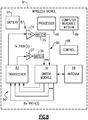
- FIG 8 is a schematic block diagram of one example of a wireless or mobile device 81 that can include one or more power amplifiers and an antenna switch module.
- the wireless device 81 can have one or more transmit paths 85 that implement one or more features of the present disclosure.
- the transmit paths 85 of the wireless device 81 can include the transmission paths in accordance with any of the principles and advantages discussed with any of Figures 1 , 3A , 4A , 5A , or Figure 6A .
- any of the band select switches and/or select switches discussed herein can be included in the switch module 16 of Figure 8 .
- the switch module 16 and the antenna 18 of Figure 8 can correspond to the switch module 16 and the antenna 18, respectively, of Figure 1 . Additional elements, such as any of the matching networks discussed herein can be disposed between the output of any of the power amplifiers 87 and the switch module 16 of Figure 8 .
- the example wireless device 81 depicted in Figure 8 can represent a multi-band and/or multi-mode device such as a multi-band/multi-mode mobile phone.
- the wireless device 81 can communicate in accordance with Long Term Evolution (LTE).
- LTE Long Term Evolution
- the wireless device can be configured to operate at one or more frequency bands defined by an LTE standard.
- the wireless device 81 can alternatively or additionally be configured to communicate in accordance with one or more other communication standards, including but not limited to one or more of a Wi-Fi standard, a 3G standard, a 4G standard or an Advanced LTE standard. Transmit paths of the present disclosure can be implemented within a mobile device implementing any combination of the foregoing example communication standards, for example.
- the wireless device 81 can include a switch module 16, a transceiver 83, an antenna 18, power amplifiers 87, matching networks 25 and 28, a control component 88, a computer readable storage medium 89, a processor 90, and a battery 91.
- the transceiver 83 can generate RF signals for transmission via the antenna 18. Furthermore, the transceiver 83 can receive incoming RF signals from the antenna 18. It will be understood that various functionalities associated with transmitting and receiving of RF signals can be achieved by one or more components that are collectively represented in Figure 8 as the transceiver 83. For example, a single component can be configured to provide both transmitting and receiving functionalities. In another example, transmitting and receiving functionalities can be provided by separate components.
- one or more output signals from the transceiver 83 are depicted as being provided to the antenna 18 via one or more transmission paths 85.
- different transmission paths 85 can represent output paths associated with different bands (e.g., a high band and a low band) and/or different power outputs.
- the two different paths shown can represent two of the different transmission paths of any of the front end architectures discussed with reference to Figures 1 , 3A , 4A , 5A , and/or 6A.
- the transmission paths 85 can be associated with different transmission modes.
- One of the illustrated transmission paths 85 can be active while one or more of the other transmission paths 85 are non-active, for example, as discussed above.
- two or more transmission paths 85 can be active in carrier aggregation applications.
- Other transmission paths 85 can be associated with different power modes (e.g., high power mode and low power mode) and/or paths associated with different transmit frequency bands.
- the transmit paths 85 can include one or more power amplifiers 87 to aid in boosting a RF signal having a relatively low power to a higher power suitable for transmission.
- the power amplifiers 87 can include the power amplifiers 24 and 27 discussed above.
- Figure 8 illustrates a configuration using two transmission paths 85, the wireless device 81 can be adapted to include more than two transmission paths 85.
- one or more detected signals from the antenna 18 are depicted as being provided to the transceiver 83 via one or more receive paths 86.
- different receive paths 86 can represent paths associated with different signaling modes and/or different receive frequency bands.
- Figure 8 illustrates a configuration using four receive paths 86, the wireless device 81 can be adapted to include more or fewer receive paths 86.
- the antenna switch module 16 can be included and can be used to selectively electrically connect the antenna 18 to a selected transmit or receive path.
- the antenna switch module 16 can provide a number of switching functionalities associated with an operation of the wireless device 81.
- the antenna switch module 16 can include a multi-throw switch configured to provide functionalities associated with, for example, switching between different bands, switching between different modes, switching between transmission and receiving modes, or any combination thereof.
- the switch module 16 can include any of the band select switches discussed herein.
- control component 88 can be provided for controlling various control functionalities associated with operations of the antenna switch module 16 and/or other operating component(s).
- control component 88 can aid in providing control signals to the antenna switch module 16 so as to select a particular transmit or receive path.
- the processor 90 can be configured to facilitate implementation of various processes on the wireless device 81.
- the processor 90 can be, for example, a general purpose processor or special purpose processor.
- the wireless device 81 can include a non-transitory computer-readable medium 89, such as a memory, which can store computer program instructions that may be provided to and executed by the processor 90.
- the battery 91 can be any battery suitable for use in the wireless device 81, including, for example, a lithium-ion battery.
- the teachings herein are applicable to a variety of power amplifier systems including systems with multiple power amplifiers, including, for example, multi-band and/or multi-mode power amplifier systems.
- the power amplifier transistors discussed herein can be, for example, gallium arsenide (GaAs), CMOS, or silicon germanium (SiGe) transistors.
- the power amplifiers discussed herein can be implemented by field effect transistors and/or bipolar transistors, such as heterojunction bipolar transistors.
- Examples of the electronic devices can include, but are not limited to, consumer electronic products, parts of the consumer electronic products, electronic test equipment, cellular communications infrastructure such as a base station, etc.
- Examples of the electronic devices can include, but are not limited to, a mobile phone such as a smart phone, a telephone, a television, a computer monitor, a computer, a modem, a hand-held computer, a laptop computer, a tablet computer, a wearable computing device such as a smart watch, a personal digital assistant (PDA), a microwave, a refrigerator, a vehicular electronics system such as automotive electronics system, a stereo system, a DVD player, a CD player, a digital music player such as an MP3 player, a radio, a camcorder, a camera, a digital camera, a portable memory chip, a washer, a dryer, a washer/dryer, a copier, a facsimile machine, a scanner, a multi-functional peripheral device,
- a mobile phone such as a smart phone
- the words “comprise,” “comprising,” “include,” “including,” and the like are to be construed in an inclusive sense, as opposed to an exclusive or exhaustive sense; that is to say, in the sense of "including, but not limited to.”
- the word “coupled”, as generally used herein, refers to two or more elements that may be either directly connected, or connected by way of one or more intermediate elements.
- the word “connected”, as generally used herein, refers to two or more elements that may be either directly connected, or connected by way of one or more intermediate elements.
- conditional language used herein such as, among others, “can,” “could,” “might,” “may,” “e.g.,” “for example,” “such as” and the like, unless specifically stated otherwise, or otherwise understood within the context as used, is generally intended to convey that certain embodiments include, while other embodiments do not include, certain features, elements and/or states.
- conditional language is not generally intended to imply that features, elements and/or states are in any way required for one or more embodiments or that one or more embodiments necessarily include logic for deciding, with or without author input or prompting, whether these features, elements and/or states are included or are to be performed in any particular embodiment.
Landscapes
- Engineering & Computer Science (AREA)
- Computer Networks & Wireless Communication (AREA)
- Signal Processing (AREA)
- Power Engineering (AREA)
- Amplifiers (AREA)
- Transmitters (AREA)
- Transceivers (AREA)
Applications Claiming Priority (1)
| Application Number | Priority Date | Filing Date | Title |
|---|---|---|---|
| US201462051191P | 2014-09-16 | 2014-09-16 |
Publications (2)
| Publication Number | Publication Date |
|---|---|
| EP2999125A1 EP2999125A1 (en) | 2016-03-23 |
| EP2999125B1 true EP2999125B1 (en) | 2018-06-06 |
Family
ID=54198945
Family Applications (1)
| Application Number | Title | Priority Date | Filing Date |
|---|---|---|---|
| EP15185429.6A Active EP2999125B1 (en) | 2014-09-16 | 2015-09-16 | Multi-band device with reduced band loading |
Country Status (6)
| Country | Link |
|---|---|
| US (4) | US9531413B2 (enExample) |
| EP (1) | EP2999125B1 (enExample) |
| JP (1) | JP6216753B2 (enExample) |
| KR (1) | KR101788396B1 (enExample) |
| CN (1) | CN105429605B (enExample) |
| TW (2) | TWI633753B (enExample) |
Families Citing this family (45)
| Publication number | Priority date | Publication date | Assignee | Title |
|---|---|---|---|---|
| US7719343B2 (en) | 2003-09-08 | 2010-05-18 | Peregrine Semiconductor Corporation | Low noise charge pump method and apparatus |
| JP4659826B2 (ja) | 2004-06-23 | 2011-03-30 | ペレグリン セミコンダクター コーポレーション | Rfフロントエンド集積回路 |
| JP6216753B2 (ja) | 2014-09-16 | 2017-10-18 | スカイワークス ソリューションズ, インコーポレイテッドSkyworks Solutions, Inc. | バンドローディングを低減するマルチバンドデバイス |
| US9543900B1 (en) * | 2015-06-19 | 2017-01-10 | Qualcomm Incorporated | Switchable supply and tunable load impedance power amplifier |
| DE102016107628A1 (de) * | 2016-04-25 | 2017-10-26 | Snaptrack, Inc. | Multiplexer-Schaltung für Tx-Carrier-Aggregation |
| JP2018042100A (ja) | 2016-09-07 | 2018-03-15 | 株式会社村田製作所 | 送信モジュール及び送受信モジュール |
| US10038414B2 (en) * | 2016-12-07 | 2018-07-31 | Psemi Corporation | RF switch with split tunable matching network |
| JP2018107502A (ja) | 2016-12-22 | 2018-07-05 | 株式会社村田製作所 | 通信モジュール |
| KR102563838B1 (ko) * | 2017-01-23 | 2023-08-07 | 삼성전자주식회사 | 전자 장치 및 전자 장치의 통신 신호 수신 경로 결정 방법 |
| CN107070492B (zh) * | 2017-03-28 | 2020-08-14 | 尚睿微电子(上海)有限公司 | 一种信号收发控制结构、方法及电子设备 |
| KR101912288B1 (ko) * | 2017-06-12 | 2018-10-29 | 삼성전기 주식회사 | 파워 증폭 시스템의 밴드 선택 스위치 장치 |
| US10772052B2 (en) * | 2017-06-16 | 2020-09-08 | Qualcomm Incorporated | Controlling coexistent radio systems in a wireless device |
| CN107395250A (zh) * | 2017-08-22 | 2017-11-24 | 上海斐讯数据通信技术有限公司 | 一种射频电路和减少射频电路谐波干扰的方法 |
| CN107707264A (zh) * | 2017-08-31 | 2018-02-16 | 希姆通信息技术(上海)有限公司 | 功率检测反馈电路及方法 |
| JP2019068205A (ja) * | 2017-09-29 | 2019-04-25 | 株式会社村田製作所 | 高周波回路、フロントエンドモジュールおよび通信装置 |
| KR102352553B1 (ko) * | 2017-10-25 | 2022-01-18 | 삼성전자주식회사 | 복수의 안테나들을 포함하는 전자 장치와 이의 동작 방법 |
| US10554177B2 (en) | 2017-11-27 | 2020-02-04 | Skyworks Solutions, Inc. | Quadrature combined doherty amplifiers |
| WO2019103899A1 (en) | 2017-11-27 | 2019-05-31 | Skyworks Solutions, Inc. | Wideband power combiner and splitter |
| KR102722507B1 (ko) * | 2017-12-07 | 2024-10-29 | 인피니언 테크놀로지스 아게 | 음향적으로 결합된 공진기 노치 및 대역 통과 필터 |
| CN112134588B (zh) * | 2018-03-16 | 2022-03-15 | Oppo广东移动通信有限公司 | 多路选择开关及相关产品 |
| CN108377151B (zh) * | 2018-03-22 | 2019-11-08 | 上海唯捷创芯电子技术有限公司 | 一种多模多频无线射频前端模块、芯片及通信终端 |
| US10727894B2 (en) | 2018-04-30 | 2020-07-28 | Skyworks Solutions, Inc. | Front end systems with switched termination for enhanced intermodulation distortion performance |
| CN108832959B (zh) * | 2018-08-29 | 2024-02-13 | Oppo(重庆)智能科技有限公司 | 射频前端模组及电子装置 |
| CN109379053B (zh) * | 2018-12-07 | 2020-09-25 | 曹秀妹 | 可切换负载线的匹配电路、负载线切换方法及功率放大器 |
| CN109547042B (zh) * | 2018-12-19 | 2020-12-22 | 天津大学 | 多通道发射机射频前端结构和终端以及无线通信设备 |
| KR102597392B1 (ko) | 2019-02-28 | 2023-11-03 | 삼성전자주식회사 | 이중 대역을 지원하는 안테나 모듈 및 이를 포함하는 전자 장치 |
| US11245432B2 (en) | 2019-03-06 | 2022-02-08 | Skyworks Solutions, Inc. | Radio frequency device with integrated antenna tuner and multiplexer |
| KR102598267B1 (ko) * | 2019-03-15 | 2023-11-06 | 삼성전자주식회사 | 안테나 커플링을 위한 전자 장치 및 방법 |
| KR102194705B1 (ko) * | 2019-03-19 | 2020-12-23 | 삼성전기주식회사 | 밴드 선택 스위치 회로 및 증폭 장치 |
| US11044671B2 (en) * | 2019-03-29 | 2021-06-22 | Intel Corporation | Communication system including a wake-up radio |
| JP2021150908A (ja) * | 2020-03-23 | 2021-09-27 | 株式会社村田製作所 | 高周波回路及び通信装置 |
| US11671122B2 (en) | 2020-08-26 | 2023-06-06 | Skyworks Solutions, Inc. | Filter reuse in radio frequency front-ends |
| KR102880875B1 (ko) * | 2020-08-26 | 2025-11-04 | 삼성전자 주식회사 | 복수의 주파수 대역을 이용한 통신을 수행하는 통신 회로와 그것을 구비한 전자 장치 |
| US11601144B2 (en) | 2020-08-26 | 2023-03-07 | Skyworks Solutions, Inc. | Broadband architectures for radio frequency front-ends |
| US12191826B2 (en) | 2020-09-29 | 2025-01-07 | Skyworks Solutions, Inc. | Method for adjusting power amplifier impedance |
| US12255372B2 (en) | 2021-09-15 | 2025-03-18 | Murata Manufacturing Co., Ltd. | Methods and circuits for stable hot switching of antennas |
| DE112022004401T5 (de) * | 2021-09-15 | 2024-07-11 | Murata Manufacturing Co., Ltd. | Verfahren und Schaltungen für stabiles Umschalten im Betrieb von Antennen |
| TWI803020B (zh) * | 2021-10-20 | 2023-05-21 | 立積電子股份有限公司 | 射頻切換器 |
| US12542568B2 (en) | 2021-11-08 | 2026-02-03 | Skyworks Solutions, Inc. | Power rugged filter module |
| CN114928368A (zh) * | 2022-01-07 | 2022-08-19 | 西安海云物联科技有限公司 | 一种用于5g频段wifi6的射频阻抗收敛的匹配电路结构 |
| US12587230B2 (en) | 2022-04-13 | 2026-03-24 | Skyworks Solutions, Inc. | Switch module with shunt switches |
| CN119213699A (zh) * | 2022-05-17 | 2024-12-27 | 株式会社村田制作所 | 放大电路以及通信装置 |
| WO2024242500A1 (ko) * | 2023-05-25 | 2024-11-28 | 삼성전자 주식회사 | 보안 연결을 제공하는 전자 장치 및 그 동작 방법 |
| TWI899758B (zh) * | 2023-12-20 | 2025-10-01 | 美商奧希羅半導體公司 | 寬頻級間匹配 |
| US20250240041A1 (en) * | 2024-01-23 | 2025-07-24 | Qualcomm Incorporated | Transmitter architecture suppressing harmonic signals between transmitters using a filter and a reconfigurable power amplifier |
Family Cites Families (48)
| Publication number | Priority date | Publication date | Assignee | Title |
|---|---|---|---|---|
| US6298244B1 (en) | 1997-07-03 | 2001-10-02 | Ericsson Inc. | Dual-band, dual-mode power amplifier |
| SE511749C2 (sv) * | 1998-04-07 | 1999-11-15 | Ericsson Telefon Ab L M | Antennomkopplare |
| US6496708B1 (en) * | 1999-09-15 | 2002-12-17 | Motorola, Inc. | Radio frequency coupler apparatus suitable for use in a multi-band wireless communication device |
| WO2001028164A1 (en) | 1999-10-14 | 2001-04-19 | Sharegate Inc. | System and method for enabling simultaneous multi-channel analog communications |
| US6625470B1 (en) | 2000-03-02 | 2003-09-23 | Motorola, Inc. | Transmitter |
| JP3874241B2 (ja) * | 2001-07-27 | 2007-01-31 | 株式会社ルネサステクノロジ | 電子部品および設計方法 |
| JP2003174335A (ja) * | 2001-12-05 | 2003-06-20 | Mitsubishi Electric Corp | 増幅器 |
| JP3747010B2 (ja) * | 2002-04-16 | 2006-02-22 | 埼玉日本電気株式会社 | 携帯無線機 |
| DE102004016399B4 (de) * | 2003-03-27 | 2013-06-06 | Kyocera Corp. | Hochfrequenzmodul und Funkvorrichtung |
| JP4659826B2 (ja) * | 2004-06-23 | 2011-03-30 | ペレグリン セミコンダクター コーポレーション | Rfフロントエンド集積回路 |
| US8000737B2 (en) * | 2004-10-15 | 2011-08-16 | Sky Cross, Inc. | Methods and apparatuses for adaptively controlling antenna parameters to enhance efficiency and maintain antenna size compactness |
| BRPI0518340B1 (pt) * | 2004-11-19 | 2018-12-04 | Huawei Tech Co Ltd | sistema e método de redundância tipo hot standby para amplificador de potência de radiofrequência |
| DE102005046452B4 (de) * | 2005-09-28 | 2021-02-25 | Snaptrack, Inc. | Multiband-Schaltung |
| JP4892253B2 (ja) * | 2006-02-28 | 2012-03-07 | ルネサスエレクトロニクス株式会社 | 電子装置 |
| US7808342B2 (en) * | 2006-10-02 | 2010-10-05 | Skyworks Solutions, Inc. | Harmonic phase tuning filter for RF switches |
| EP2078337B1 (en) * | 2006-10-25 | 2015-07-01 | Nxp B.V. | Determining on chip load impedance of rf circuit |
| US20080136559A1 (en) * | 2006-12-08 | 2008-06-12 | Wataru Takahashi | Electronic device and rf module |
| US7925227B2 (en) | 2007-09-19 | 2011-04-12 | Micro Mobio Corporation | Multi-band amplifier module with harmonic suppression |
| US20090180403A1 (en) | 2008-01-11 | 2009-07-16 | Bogdan Tudosoiu | Multi-band and multi-mode radio frequency front-end module architecture |
| US8971830B2 (en) | 2009-05-12 | 2015-03-03 | Qualcomm Incorporated | Multi-mode multi-band power amplifier module |
| CN201479386U (zh) * | 2009-07-24 | 2010-05-19 | 惠州Tcl移动通信有限公司 | 多天线无线收发装置 |
| US8306481B2 (en) | 2009-10-30 | 2012-11-06 | Infineon Technologies Ag | Single pole multi throw switch |
| US8774067B2 (en) | 2009-11-17 | 2014-07-08 | Nokia Corporation | Antenna impedance stabilization with stabilization load in second antenna circuitry |
| US8537723B2 (en) | 2010-03-12 | 2013-09-17 | Rf Micro Devices, Inc. | LTE-Advanced (4G) front end radio architecture |
| JP5170139B2 (ja) * | 2010-03-23 | 2013-03-27 | 株式会社村田製作所 | 回路モジュール |
| WO2011133657A2 (en) | 2010-04-20 | 2011-10-27 | Paratek Microwave, Inc. | Method and apparatus for managing interference in a communication device |
| US9948348B2 (en) * | 2010-05-26 | 2018-04-17 | Skyworks Solutions, Inc. | High isolation switch with notch filter |
| KR101675342B1 (ko) * | 2010-06-01 | 2016-11-11 | 삼성전자주식회사 | 휴대용 단말기의 전력 증폭 장치 및 방법 |
| US8725085B2 (en) * | 2010-06-03 | 2014-05-13 | Broadcom Corporation | RF front-end module |
| CN101917167B (zh) * | 2010-08-24 | 2014-05-14 | 惠州市正源微电子有限公司 | 射频功率放大器功率合成电路 |
| JP5467979B2 (ja) | 2010-09-14 | 2014-04-09 | ルネサスエレクトロニクス株式会社 | 高周波モジュール |
| WO2012157645A1 (ja) * | 2011-05-18 | 2012-11-22 | 株式会社村田製作所 | 電力増幅器およびその動作方法 |
| US9143125B2 (en) * | 2011-11-09 | 2015-09-22 | Skyworks Solutions, Inc. | Radio-frequency switches having extended termination bandwidth and related circuits, modules, methods, and systems |
| GB2498212B (en) | 2012-01-09 | 2013-12-04 | Renesas Mobile Corp | Method and apparatus for time division duplex communication |
| US9263793B2 (en) * | 2012-04-20 | 2016-02-16 | Ethertronics, Inc. | Multi-band communication system with isolation and impedance matching provision |
| US8843083B2 (en) | 2012-07-09 | 2014-09-23 | Rf Micro Devices (Cayman Islands), Ltd. | CMOS switching circuitry of a transmitter module |
| US8933858B2 (en) * | 2012-08-09 | 2015-01-13 | Qualcomm Incorporated | Front end parallel resonant switch |
| US9692392B2 (en) * | 2012-09-11 | 2017-06-27 | Qualcomm Incorporated | Filters for multi-band wireless device |
| TWI492549B (zh) * | 2012-10-09 | 2015-07-11 | Realtek Semiconductor Corp | 多模式功率放大電路、多模式無線發射模組及其方法 |
| US9236663B2 (en) * | 2013-03-22 | 2016-01-12 | Apple Inc. | Electronic device having adaptive filter circuitry for blocking interference between wireless transceivers |
| TWI523441B (zh) * | 2013-03-25 | 2016-02-21 | Radio front end module | |
| US9300286B2 (en) * | 2013-09-27 | 2016-03-29 | Peregrine Semiconductor Corporation | Antenna transmit receive switch |
| US9257756B2 (en) | 2013-09-30 | 2016-02-09 | Novatel, Inc. | Dual band directive/reflective antenna |
| JP5900756B2 (ja) | 2014-02-28 | 2016-04-06 | 株式会社村田製作所 | 電力増幅モジュール |
| US20150270813A1 (en) | 2014-03-20 | 2015-09-24 | Qualcomm Incorporated | Dynamically adjustable power amplifier load tuner |
| US9515645B2 (en) * | 2014-06-03 | 2016-12-06 | Infineon Technologies Ag | System and method for a radio frequency switch |
| US9231550B2 (en) | 2014-06-09 | 2016-01-05 | Mitsubishi Electric Research Laboratories, Inc. | Output matching network for wideband power amplifier with harmonic suppression |
| JP6216753B2 (ja) | 2014-09-16 | 2017-10-18 | スカイワークス ソリューションズ, インコーポレイテッドSkyworks Solutions, Inc. | バンドローディングを低減するマルチバンドデバイス |
-
2015
- 2015-09-15 JP JP2015181601A patent/JP6216753B2/ja active Active
- 2015-09-15 US US14/855,141 patent/US9531413B2/en active Active
- 2015-09-15 US US14/855,103 patent/US9647703B2/en active Active
- 2015-09-15 CN CN201510585392.7A patent/CN105429605B/zh active Active
- 2015-09-16 KR KR1020150131081A patent/KR101788396B1/ko active Active
- 2015-09-16 EP EP15185429.6A patent/EP2999125B1/en active Active
- 2015-09-16 TW TW106123540A patent/TWI633753B/zh active
- 2015-09-16 TW TW104130696A patent/TWI623196B/zh active
-
2017
- 2017-03-27 US US15/470,729 patent/US10224977B2/en active Active
-
2019
- 2019-01-15 US US16/248,041 patent/US10623046B2/en active Active
Non-Patent Citations (1)
| Title |
|---|
| None * |
Also Published As
| Publication number | Publication date |
|---|---|
| US9647703B2 (en) | 2017-05-09 |
| US20160080011A1 (en) | 2016-03-17 |
| TWI633753B (zh) | 2018-08-21 |
| HK1216463A1 (zh) | 2016-11-11 |
| KR101788396B1 (ko) | 2017-10-20 |
| US9531413B2 (en) | 2016-12-27 |
| CN105429605A (zh) | 2016-03-23 |
| TW201616808A (zh) | 2016-05-01 |
| US20190245577A1 (en) | 2019-08-08 |
| JP6216753B2 (ja) | 2017-10-18 |
| EP2999125A1 (en) | 2016-03-23 |
| US20160080012A1 (en) | 2016-03-17 |
| US20170230075A1 (en) | 2017-08-10 |
| US10224977B2 (en) | 2019-03-05 |
| TW201735532A (zh) | 2017-10-01 |
| JP2016063539A (ja) | 2016-04-25 |
| US10623046B2 (en) | 2020-04-14 |
| KR20160032704A (ko) | 2016-03-24 |
| TWI623196B (zh) | 2018-05-01 |
| CN105429605B (zh) | 2019-03-08 |
Similar Documents
| Publication | Publication Date | Title |
|---|---|---|
| US10623046B2 (en) | Multi-band device with reduced band loading | |
| US10553570B2 (en) | Network with integrated passive device and conductive trace in packaging substrate and related modules and devices | |
| US10447323B2 (en) | Bypass path loss reduction | |
| US8983406B2 (en) | Signal path termination | |
| US11711105B2 (en) | Wireless amplifier circuitry for carrier aggregation | |
| KR101793148B1 (ko) | 멀티-대역 전력 증폭기 | |
| US11277158B2 (en) | Semiconductor device | |
| HK1216463B (zh) | 具有減小的頻帶加載的多頻帶設備 | |
| US20240088840A1 (en) | Wireless Amplifier Circuitry | |
| HK1232683A1 (en) | Network with integrated passive device and conductive trace in packaging substrate and related modules and devices | |
| HK1232683B (zh) | 具有集成無源器件和導電跡線的網絡、有關模塊和裝置 | |
| HK1211390B (zh) | 旁路路徑損耗減少 |
Legal Events
| Date | Code | Title | Description |
|---|---|---|---|
| PUAI | Public reference made under article 153(3) epc to a published international application that has entered the european phase |
Free format text: ORIGINAL CODE: 0009012 |
|
| AK | Designated contracting states |
Kind code of ref document: A1 Designated state(s): AL AT BE BG CH CY CZ DE DK EE ES FI FR GB GR HR HU IE IS IT LI LT LU LV MC MK MT NL NO PL PT RO RS SE SI SK SM TR |
|
| AX | Request for extension of the european patent |
Extension state: BA ME |
|
| 17P | Request for examination filed |
Effective date: 20160915 |
|
| RBV | Designated contracting states (corrected) |
Designated state(s): AL AT BE BG CH CY CZ DE DK EE ES FI FR GB GR HR HU IE IS IT LI LT LU LV MC MK MT NL NO PL PT RO RS SE SI SK SM TR |
|
| REG | Reference to a national code |
Ref country code: DE Ref legal event code: R079 Ref document number: 602015011686 Country of ref document: DE Free format text: PREVIOUS MAIN CLASS: H04B0001000000 Ipc: H04B0001040000 |
|
| GRAP | Despatch of communication of intention to grant a patent |
Free format text: ORIGINAL CODE: EPIDOSNIGR1 |
|
| STAA | Information on the status of an ep patent application or granted ep patent |
Free format text: STATUS: GRANT OF PATENT IS INTENDED |
|
| RIC1 | Information provided on ipc code assigned before grant |
Ipc: H04B 1/00 20060101ALI20171123BHEP Ipc: H04B 1/04 20060101AFI20171123BHEP |
|
| INTG | Intention to grant announced |
Effective date: 20171222 |
|
| GRAS | Grant fee paid |
Free format text: ORIGINAL CODE: EPIDOSNIGR3 |
|
| GRAA | (expected) grant |
Free format text: ORIGINAL CODE: 0009210 |
|
| STAA | Information on the status of an ep patent application or granted ep patent |
Free format text: STATUS: THE PATENT HAS BEEN GRANTED |
|
| AK | Designated contracting states |
Kind code of ref document: B1 Designated state(s): AL AT BE BG CH CY CZ DE DK EE ES FI FR GB GR HR HU IE IS IT LI LT LU LV MC MK MT NL NO PL PT RO RS SE SI SK SM TR |
|
| REG | Reference to a national code |
Ref country code: GB Ref legal event code: FG4D |
|
| REG | Reference to a national code |
Ref country code: CH Ref legal event code: EP Ref country code: AT Ref legal event code: REF Ref document number: 1007159 Country of ref document: AT Kind code of ref document: T Effective date: 20180615 |
|
| REG | Reference to a national code |
Ref country code: IE Ref legal event code: FG4D |
|
| REG | Reference to a national code |
Ref country code: DE Ref legal event code: R096 Ref document number: 602015011686 Country of ref document: DE |
|
| REG | Reference to a national code |
Ref country code: FR Ref legal event code: PLFP Year of fee payment: 4 |
|
| REG | Reference to a national code |
Ref country code: NL Ref legal event code: MP Effective date: 20180606 |
|
| REG | Reference to a national code |
Ref country code: LT Ref legal event code: MG4D |
|
| PG25 | Lapsed in a contracting state [announced via postgrant information from national office to epo] |
Ref country code: CY Free format text: LAPSE BECAUSE OF FAILURE TO SUBMIT A TRANSLATION OF THE DESCRIPTION OR TO PAY THE FEE WITHIN THE PRESCRIBED TIME-LIMIT Effective date: 20180606 Ref country code: LT Free format text: LAPSE BECAUSE OF FAILURE TO SUBMIT A TRANSLATION OF THE DESCRIPTION OR TO PAY THE FEE WITHIN THE PRESCRIBED TIME-LIMIT Effective date: 20180606 Ref country code: SE Free format text: LAPSE BECAUSE OF FAILURE TO SUBMIT A TRANSLATION OF THE DESCRIPTION OR TO PAY THE FEE WITHIN THE PRESCRIBED TIME-LIMIT Effective date: 20180606 Ref country code: FI Free format text: LAPSE BECAUSE OF FAILURE TO SUBMIT A TRANSLATION OF THE DESCRIPTION OR TO PAY THE FEE WITHIN THE PRESCRIBED TIME-LIMIT Effective date: 20180606 Ref country code: BG Free format text: LAPSE BECAUSE OF FAILURE TO SUBMIT A TRANSLATION OF THE DESCRIPTION OR TO PAY THE FEE WITHIN THE PRESCRIBED TIME-LIMIT Effective date: 20180906 Ref country code: ES Free format text: LAPSE BECAUSE OF FAILURE TO SUBMIT A TRANSLATION OF THE DESCRIPTION OR TO PAY THE FEE WITHIN THE PRESCRIBED TIME-LIMIT Effective date: 20180606 Ref country code: NO Free format text: LAPSE BECAUSE OF FAILURE TO SUBMIT A TRANSLATION OF THE DESCRIPTION OR TO PAY THE FEE WITHIN THE PRESCRIBED TIME-LIMIT Effective date: 20180906 |
|
| PG25 | Lapsed in a contracting state [announced via postgrant information from national office to epo] |
Ref country code: LV Free format text: LAPSE BECAUSE OF FAILURE TO SUBMIT A TRANSLATION OF THE DESCRIPTION OR TO PAY THE FEE WITHIN THE PRESCRIBED TIME-LIMIT Effective date: 20180606 Ref country code: HR Free format text: LAPSE BECAUSE OF FAILURE TO SUBMIT A TRANSLATION OF THE DESCRIPTION OR TO PAY THE FEE WITHIN THE PRESCRIBED TIME-LIMIT Effective date: 20180606 Ref country code: GR Free format text: LAPSE BECAUSE OF FAILURE TO SUBMIT A TRANSLATION OF THE DESCRIPTION OR TO PAY THE FEE WITHIN THE PRESCRIBED TIME-LIMIT Effective date: 20180907 Ref country code: RS Free format text: LAPSE BECAUSE OF FAILURE TO SUBMIT A TRANSLATION OF THE DESCRIPTION OR TO PAY THE FEE WITHIN THE PRESCRIBED TIME-LIMIT Effective date: 20180606 |
|
| REG | Reference to a national code |
Ref country code: AT Ref legal event code: MK05 Ref document number: 1007159 Country of ref document: AT Kind code of ref document: T Effective date: 20180606 |
|
| PG25 | Lapsed in a contracting state [announced via postgrant information from national office to epo] |
Ref country code: NL Free format text: LAPSE BECAUSE OF FAILURE TO SUBMIT A TRANSLATION OF THE DESCRIPTION OR TO PAY THE FEE WITHIN THE PRESCRIBED TIME-LIMIT Effective date: 20180606 |
|
| PG25 | Lapsed in a contracting state [announced via postgrant information from national office to epo] |
Ref country code: AT Free format text: LAPSE BECAUSE OF FAILURE TO SUBMIT A TRANSLATION OF THE DESCRIPTION OR TO PAY THE FEE WITHIN THE PRESCRIBED TIME-LIMIT Effective date: 20180606 Ref country code: PL Free format text: LAPSE BECAUSE OF FAILURE TO SUBMIT A TRANSLATION OF THE DESCRIPTION OR TO PAY THE FEE WITHIN THE PRESCRIBED TIME-LIMIT Effective date: 20180606 Ref country code: CZ Free format text: LAPSE BECAUSE OF FAILURE TO SUBMIT A TRANSLATION OF THE DESCRIPTION OR TO PAY THE FEE WITHIN THE PRESCRIBED TIME-LIMIT Effective date: 20180606 Ref country code: SK Free format text: LAPSE BECAUSE OF FAILURE TO SUBMIT A TRANSLATION OF THE DESCRIPTION OR TO PAY THE FEE WITHIN THE PRESCRIBED TIME-LIMIT Effective date: 20180606 Ref country code: RO Free format text: LAPSE BECAUSE OF FAILURE TO SUBMIT A TRANSLATION OF THE DESCRIPTION OR TO PAY THE FEE WITHIN THE PRESCRIBED TIME-LIMIT Effective date: 20180606 Ref country code: IS Free format text: LAPSE BECAUSE OF FAILURE TO SUBMIT A TRANSLATION OF THE DESCRIPTION OR TO PAY THE FEE WITHIN THE PRESCRIBED TIME-LIMIT Effective date: 20181006 Ref country code: EE Free format text: LAPSE BECAUSE OF FAILURE TO SUBMIT A TRANSLATION OF THE DESCRIPTION OR TO PAY THE FEE WITHIN THE PRESCRIBED TIME-LIMIT Effective date: 20180606 |
|
| PG25 | Lapsed in a contracting state [announced via postgrant information from national office to epo] |
Ref country code: SM Free format text: LAPSE BECAUSE OF FAILURE TO SUBMIT A TRANSLATION OF THE DESCRIPTION OR TO PAY THE FEE WITHIN THE PRESCRIBED TIME-LIMIT Effective date: 20180606 Ref country code: IT Free format text: LAPSE BECAUSE OF FAILURE TO SUBMIT A TRANSLATION OF THE DESCRIPTION OR TO PAY THE FEE WITHIN THE PRESCRIBED TIME-LIMIT Effective date: 20180606 |
|
| REG | Reference to a national code |
Ref country code: DE Ref legal event code: R097 Ref document number: 602015011686 Country of ref document: DE |
|
| PLBE | No opposition filed within time limit |
Free format text: ORIGINAL CODE: 0009261 |
|
| STAA | Information on the status of an ep patent application or granted ep patent |
Free format text: STATUS: NO OPPOSITION FILED WITHIN TIME LIMIT |
|
| PG25 | Lapsed in a contracting state [announced via postgrant information from national office to epo] |
Ref country code: MC Free format text: LAPSE BECAUSE OF FAILURE TO SUBMIT A TRANSLATION OF THE DESCRIPTION OR TO PAY THE FEE WITHIN THE PRESCRIBED TIME-LIMIT Effective date: 20180606 |
|
| REG | Reference to a national code |
Ref country code: CH Ref legal event code: PL |
|
| 26N | No opposition filed |
Effective date: 20190307 |
|
| PG25 | Lapsed in a contracting state [announced via postgrant information from national office to epo] |
Ref country code: SI Free format text: LAPSE BECAUSE OF FAILURE TO SUBMIT A TRANSLATION OF THE DESCRIPTION OR TO PAY THE FEE WITHIN THE PRESCRIBED TIME-LIMIT Effective date: 20180606 Ref country code: DK Free format text: LAPSE BECAUSE OF FAILURE TO SUBMIT A TRANSLATION OF THE DESCRIPTION OR TO PAY THE FEE WITHIN THE PRESCRIBED TIME-LIMIT Effective date: 20180606 |
|
| REG | Reference to a national code |
Ref country code: BE Ref legal event code: MM Effective date: 20180930 |
|
| REG | Reference to a national code |
Ref country code: IE Ref legal event code: MM4A |
|
| PG25 | Lapsed in a contracting state [announced via postgrant information from national office to epo] |
Ref country code: LU Free format text: LAPSE BECAUSE OF NON-PAYMENT OF DUE FEES Effective date: 20180916 |
|
| PG25 | Lapsed in a contracting state [announced via postgrant information from national office to epo] |
Ref country code: IE Free format text: LAPSE BECAUSE OF NON-PAYMENT OF DUE FEES Effective date: 20180916 |
|
| PG25 | Lapsed in a contracting state [announced via postgrant information from national office to epo] |
Ref country code: LI Free format text: LAPSE BECAUSE OF NON-PAYMENT OF DUE FEES Effective date: 20180930 Ref country code: BE Free format text: LAPSE BECAUSE OF NON-PAYMENT OF DUE FEES Effective date: 20180930 Ref country code: CH Free format text: LAPSE BECAUSE OF NON-PAYMENT OF DUE FEES Effective date: 20180930 |
|
| PG25 | Lapsed in a contracting state [announced via postgrant information from national office to epo] |
Ref country code: AL Free format text: LAPSE BECAUSE OF FAILURE TO SUBMIT A TRANSLATION OF THE DESCRIPTION OR TO PAY THE FEE WITHIN THE PRESCRIBED TIME-LIMIT Effective date: 20180606 |
|
| PG25 | Lapsed in a contracting state [announced via postgrant information from national office to epo] |
Ref country code: MT Free format text: LAPSE BECAUSE OF NON-PAYMENT OF DUE FEES Effective date: 20180916 |
|
| PG25 | Lapsed in a contracting state [announced via postgrant information from national office to epo] |
Ref country code: TR Free format text: LAPSE BECAUSE OF FAILURE TO SUBMIT A TRANSLATION OF THE DESCRIPTION OR TO PAY THE FEE WITHIN THE PRESCRIBED TIME-LIMIT Effective date: 20180606 |
|
| PG25 | Lapsed in a contracting state [announced via postgrant information from national office to epo] |
Ref country code: PT Free format text: LAPSE BECAUSE OF FAILURE TO SUBMIT A TRANSLATION OF THE DESCRIPTION OR TO PAY THE FEE WITHIN THE PRESCRIBED TIME-LIMIT Effective date: 20180606 |
|
| PG25 | Lapsed in a contracting state [announced via postgrant information from national office to epo] |
Ref country code: MK Free format text: LAPSE BECAUSE OF NON-PAYMENT OF DUE FEES Effective date: 20180606 Ref country code: HU Free format text: LAPSE BECAUSE OF FAILURE TO SUBMIT A TRANSLATION OF THE DESCRIPTION OR TO PAY THE FEE WITHIN THE PRESCRIBED TIME-LIMIT; INVALID AB INITIO Effective date: 20150916 |
|
| PGFP | Annual fee paid to national office [announced via postgrant information from national office to epo] |
Ref country code: DE Payment date: 20250929 Year of fee payment: 11 |
|
| PGFP | Annual fee paid to national office [announced via postgrant information from national office to epo] |
Ref country code: GB Payment date: 20250929 Year of fee payment: 11 |
|
| PGFP | Annual fee paid to national office [announced via postgrant information from national office to epo] |
Ref country code: FR Payment date: 20250925 Year of fee payment: 11 |