EP2999017B1 - Organische fotovoltaische zelle - Google Patents
Organische fotovoltaische zelle Download PDFInfo
- Publication number
- EP2999017B1 EP2999017B1 EP14810301.3A EP14810301A EP2999017B1 EP 2999017 B1 EP2999017 B1 EP 2999017B1 EP 14810301 A EP14810301 A EP 14810301A EP 2999017 B1 EP2999017 B1 EP 2999017B1
- Authority
- EP
- European Patent Office
- Prior art keywords
- electrode
- solar cell
- organic solar
- auxiliary electrode
- present specification
- Prior art date
- Legal status (The legal status is an assumption and is not a legal conclusion. Google has not performed a legal analysis and makes no representation as to the accuracy of the status listed.)
- Active
Links
Images
Classifications
-
- H—ELECTRICITY
- H10—SEMICONDUCTOR DEVICES; ELECTRIC SOLID-STATE DEVICES NOT OTHERWISE PROVIDED FOR
- H10K—ORGANIC ELECTRIC SOLID-STATE DEVICES
- H10K30/00—Organic devices sensitive to infrared radiation, light, electromagnetic radiation of shorter wavelength or corpuscular radiation
-
- H—ELECTRICITY
- H10—SEMICONDUCTOR DEVICES; ELECTRIC SOLID-STATE DEVICES NOT OTHERWISE PROVIDED FOR
- H10K—ORGANIC ELECTRIC SOLID-STATE DEVICES
- H10K30/00—Organic devices sensitive to infrared radiation, light, electromagnetic radiation of shorter wavelength or corpuscular radiation
- H10K30/80—Constructional details
- H10K30/81—Electrodes
- H10K30/82—Transparent electrodes, e.g. indium tin oxide [ITO] electrodes
- H10K30/83—Transparent electrodes, e.g. indium tin oxide [ITO] electrodes comprising arrangements for extracting the current from the cell, e.g. metal finger grid systems to reduce the serial resistance of transparent electrodes
-
- H—ELECTRICITY
- H10—SEMICONDUCTOR DEVICES; ELECTRIC SOLID-STATE DEVICES NOT OTHERWISE PROVIDED FOR
- H10K—ORGANIC ELECTRIC SOLID-STATE DEVICES
- H10K30/00—Organic devices sensitive to infrared radiation, light, electromagnetic radiation of shorter wavelength or corpuscular radiation
- H10K30/30—Organic devices sensitive to infrared radiation, light, electromagnetic radiation of shorter wavelength or corpuscular radiation comprising bulk heterojunctions, e.g. interpenetrating networks of donor and acceptor material domains
-
- H—ELECTRICITY
- H10—SEMICONDUCTOR DEVICES; ELECTRIC SOLID-STATE DEVICES NOT OTHERWISE PROVIDED FOR
- H10K—ORGANIC ELECTRIC SOLID-STATE DEVICES
- H10K30/00—Organic devices sensitive to infrared radiation, light, electromagnetic radiation of shorter wavelength or corpuscular radiation
- H10K30/80—Constructional details
- H10K30/81—Electrodes
- H10K30/82—Transparent electrodes, e.g. indium tin oxide [ITO] electrodes
-
- H—ELECTRICITY
- H10—SEMICONDUCTOR DEVICES; ELECTRIC SOLID-STATE DEVICES NOT OTHERWISE PROVIDED FOR
- H10K—ORGANIC ELECTRIC SOLID-STATE DEVICES
- H10K30/00—Organic devices sensitive to infrared radiation, light, electromagnetic radiation of shorter wavelength or corpuscular radiation
- H10K30/80—Constructional details
- H10K30/87—Light-trapping means
-
- H—ELECTRICITY
- H10—SEMICONDUCTOR DEVICES; ELECTRIC SOLID-STATE DEVICES NOT OTHERWISE PROVIDED FOR
- H10K—ORGANIC ELECTRIC SOLID-STATE DEVICES
- H10K2102/00—Constructional details relating to the organic devices covered by this subclass
- H10K2102/10—Transparent electrodes, e.g. using graphene
- H10K2102/101—Transparent electrodes, e.g. using graphene comprising transparent conductive oxides [TCO]
- H10K2102/103—Transparent electrodes, e.g. using graphene comprising transparent conductive oxides [TCO] comprising indium oxides, e.g. ITO
-
- H—ELECTRICITY
- H10—SEMICONDUCTOR DEVICES; ELECTRIC SOLID-STATE DEVICES NOT OTHERWISE PROVIDED FOR
- H10K—ORGANIC ELECTRIC SOLID-STATE DEVICES
- H10K30/00—Organic devices sensitive to infrared radiation, light, electromagnetic radiation of shorter wavelength or corpuscular radiation
- H10K30/50—Photovoltaic [PV] devices
-
- H—ELECTRICITY
- H10—SEMICONDUCTOR DEVICES; ELECTRIC SOLID-STATE DEVICES NOT OTHERWISE PROVIDED FOR
- H10K—ORGANIC ELECTRIC SOLID-STATE DEVICES
- H10K85/00—Organic materials used in the body or electrodes of devices covered by this subclass
- H10K85/10—Organic polymers or oligomers
- H10K85/111—Organic polymers or oligomers comprising aromatic, heteroaromatic, or aryl chains, e.g. polyaniline, polyphenylene or polyphenylene vinylene
- H10K85/113—Heteroaromatic compounds comprising sulfur or selene, e.g. polythiophene
- H10K85/1135—Polyethylene dioxythiophene [PEDOT]; Derivatives thereof
-
- Y—GENERAL TAGGING OF NEW TECHNOLOGICAL DEVELOPMENTS; GENERAL TAGGING OF CROSS-SECTIONAL TECHNOLOGIES SPANNING OVER SEVERAL SECTIONS OF THE IPC; TECHNICAL SUBJECTS COVERED BY FORMER USPC CROSS-REFERENCE ART COLLECTIONS [XRACs] AND DIGESTS
- Y02—TECHNOLOGIES OR APPLICATIONS FOR MITIGATION OR ADAPTATION AGAINST CLIMATE CHANGE
- Y02E—REDUCTION OF GREENHOUSE GAS [GHG] EMISSIONS, RELATED TO ENERGY GENERATION, TRANSMISSION OR DISTRIBUTION
- Y02E10/00—Energy generation through renewable energy sources
- Y02E10/50—Photovoltaic [PV] energy
- Y02E10/549—Organic PV cells
-
- Y—GENERAL TAGGING OF NEW TECHNOLOGICAL DEVELOPMENTS; GENERAL TAGGING OF CROSS-SECTIONAL TECHNOLOGIES SPANNING OVER SEVERAL SECTIONS OF THE IPC; TECHNICAL SUBJECTS COVERED BY FORMER USPC CROSS-REFERENCE ART COLLECTIONS [XRACs] AND DIGESTS
- Y02—TECHNOLOGIES OR APPLICATIONS FOR MITIGATION OR ADAPTATION AGAINST CLIMATE CHANGE
- Y02P—CLIMATE CHANGE MITIGATION TECHNOLOGIES IN THE PRODUCTION OR PROCESSING OF GOODS
- Y02P70/00—Climate change mitigation technologies in the production process for final industrial or consumer products
- Y02P70/50—Manufacturing or production processes characterised by the final manufactured product
Definitions
- the present specification relates to an organic solar cell and a method of manufacturing the same.
- the solar cell is a semiconductor device converting solar light into electricity by using a photovoltaic effect, and a solar cell using an inorganic semiconductor material such as a silicon or compound semiconductor has already come onto the market to be used. Further, recently, an organic solar cell using an organic material such as a polymer resin has been studied.
- Light conversion efficiency of the organic solar cell is conversion efficiency of an incident light into electric energy, and refers to efficiency that the incident light excites an organic material in a photoactive layer to form an exciton that is a form where electrons and holes are unstably combined and the electrons and the holes pass through a donor layer and an acceptor layer, respectively, and move to an electrode to be converted into electric energy.
- a material for the organic solar cell may be largely divided into a p-type organic semiconductor material that is a donor and an n-type organic semiconductor material that is an acceptor. If the exciton is generated by absorbing light, the p-type organic semiconductor material is the donor which may be divided into the holes and the electrons at a junction with the n-type organic semiconductor material to provide the electrons well.
- the n-type organic semiconductor material refers to a material which may be reduced into the acceptor to accept the electrons well.
- Various donor and acceptor materials have been reported, but it is difficult to expect efficiency of 3% or more except for P3HT/PCBM, PCPDTBT/PCBM, or the like.
- the organic solar cell has efficiency which is lower than that of the inorganic solar cell is because the organic solar cell has charge mobility that is much lower than that of the inorganic solar cell.
- a thickness of the photoactive layer is increased in order to increase light absorption, due to a reduction in charge mobility and electric field, since re-combination of charges is increased, there is a limit in improving efficiency, and in the case where a large-area cell is manufactured in order to embody a module, due to an increase in resistance of a transparent electrode, an efficiency reduction (cell to module loss) significantly occurs.
- a novel module structure using an optical spacer, metal nanoparticles, and the like, or minimizing electrode resistance has been proposed.
- the document EP 2 413 371 A2 discloses an electrode structure for a solar cell device, said electrode comprises a transparent conductive layer and a metal electrode layer and a protection layer.
- the document WO 2010/017590 A1 discloses an electrode structure for a flexible solar cell device.
- the present specification has been made in an effort to provide an organic solar cell capable of increasing light conversion efficiency and a method of manufacturing the same.
- the present specification provides an organic solar cell including: a first electrode; a second electrode provided to face the first electrode; an organic material layer of one or more layers including a photoactive layer provided between the first electrode and the second electrode; and an auxiliary electrode provided to come into contact with the first electrode, in which in the auxiliary electrode, an area of a surface close to the first electrode which an incident light reaches is smaller than an area of a facing surface thereof.
- the present specification provides a method of manufacturing the organic solar cell. Specifically, there is provided a method of manufacturing the organic solar cell, the method including: preparing a substrate; forming a first electrode on the substrate; forming an auxiliary electrode on the first electrode; forming an organic material layer of one or more layers including a photoactive layer on the auxiliary electrode; and forming a second electrode on the organic material layer, in which areas of an upper surface and a lower surface of the auxiliary electrode are different from each other.
- An organic solar cell of the present specification has high light absorption efficiency by increasing a quantity of light reaching a photoactive layer.
- the organic solar cell of the present specification has high light absorption efficiency by enabling light to be re-absorbed.
- the organic solar cell of the present specification it is possible to embody a high fill factor when a large-area device is manufactured by reducing resistance of an electrode.
- An exemplary embodiment of the present specification provides an organic solar cell including: a first electrode; a second electrode provided to face the first electrode; an organic material layer of one or more layers including a photoactive layer provided between the first electrode and the second electrode; and an auxiliary electrode provided to come into contact with the first electrode, in which in the auxiliary electrode, an area of a surface close to the first electrode which an incident light reaches is smaller than an area of a facing surface thereof.
- the present inventors introduced the auxiliary electrode in order to solve a high resistance value of a transparent electrode, and developed the organic solar cell capable of increasing light absorption efficiency by adjusting a shape of the auxiliary electrode.
- the first electrode of the organic solar cell may be a transparent electrode for light absorption.
- the transparent electrode has a problem in that transmittance is high but electric conductivity is low. Therefore, according to the exemplary embodiment of the present specification, in order to compensate for low electric conductivity of the transparent electrode, the auxiliary electrode having high conductivity on the transparent electrode may be used.
- the auxiliary electrode may be made of a metal material for high electric conductivity, and in order to reduce a problem of a reduction in transmittance of light caused by this, an area of a surface close to an electrode which the incident light reaches may be smaller than an area of a facing surface thereof.
- the incident light reaches the first electrode, and in the auxiliary electrode, an area of a surface coming into contact with the first electrode may be smaller than an area of a facing surface thereof.
- This case may mean the case where the first electrode is the transparent electrode and light is incident on the transparent electrode.
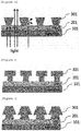
- FIG. 1 illustrates the shape of the auxiliary electrode in the organic solar cell according to the exemplary embodiment of the present specification.
- FIG. 1 illustrates an auxiliary electrode 301 provided on a first electrode 201 provided on a substrate 101.
- FIG. 1 illustrates a cross-section of the case where the auxiliary electrode is formed on the first electrode formed of ITO and light is transmitted.
- the arrow means light that is incident.
- FIG. 1 it can be seen that since the area of the auxiliary electrode on which the light is incident is small, more light may be transmitted through the first electrode, and the incident light may be reflected to a lateral surface of the auxiliary electrode to be re-absorbed into the photoactive layer.
- FIG. 1 illustrates only an effect in the case where light is incident in a vertical direction on the first electrode, but even in the case where light is incident in an incident direction that is not vertical, the same effect may be implemented.
- light that is not absorbed into the photoactive layer but is reflected out from the second electrode may be re-reflected by the auxiliary electrode to be absorbed into the photoactive layer.
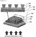
- FIG. 4 illustrates an example of the organic solar cell according to the exemplary embodiment of the present specification. Specifically, FIG. 4 illustrates an organic solar cell where a first electrode 201, an auxiliary electrode 301, a hole transport layer 401, a photoactive layer 501, and a second electrode 601 are sequentially provided on a substrate 101. FIG. 4 illustrates a shape of a cross-section of the auxiliary electrode in the case where light is incident on the first electrode.
- the incident light reaches the second electrode, and in the auxiliary electrode, an area of a surface coming into contact with the first electrode may be larger than an area of a facing surface thereof.
- This may be an organic solar cell of an inverted direction structure, in which the second electrode is the transparent electrode. That is, in the case where light is incident on the second electrode of the organic solar cell, in the auxiliary electrode, the area of the surface coming into contact with the first electrode may be larger than the area of the facing surface thereof.
- a residual light that is transmitted through the second electrode and is not absorbed in the photoactive layer may be reflected by the auxiliary electrode to be re-absorbed.
- due to the auxiliary electrode a quantity of light emitted to the first electrode may be reduced, and light may be re-absorbed to increase light absorption efficiency.
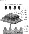
- FIG. 5 illustrates an example of the organic solar cell according to the exemplary embodiment of the present specification.
- FIG. 5 illustrates an organic solar cell where a first electrode 201, an auxiliary electrode 301, a hole transport layer 401, a photoactive layer 501, and a second electrode 601 are sequentially provided on a substrate 101.
- FIG. 5 illustrates a shape of a cross-section of the auxiliary electrode in the case where light is incident on the second electrode. That is, in FIG. 5 , as compared to an area where a residual light transmitted through the second electrode and the photoactive layer is emitted through the first electrode, a reflection area of light by the auxiliary electrode is larger, and thus the residual light reflected by the auxiliary electrode may be re-absorbed into the photoactive layer.
- a direct light may be incident on the second electrode, and a residual light that is not absorbed into the photoactive layer may be reflected by the auxiliary electrode provided on the first electrode to be re-absorbed into the photoactive layer.
- efficiency of the organic solar cell may be further increased.
- a vertical cross-section of the auxiliary electrode may have a trapezoid shape.
- the vertical cross-section means a cross-section that is vertical to a wide surface of the first electrode by configuring the wide surface of the first electrode as a horizontal surface.
- a ratio of line widths of an upper surface and a lower surface may be 1 : 1.3 to 1 : 2 or 1.3 : 1 to 3 : 1.
- lower surface may mean one surface of the auxiliary electrode closest to the first or second electrode which the incident light reaches
- upper surface may mean one surface of the auxiliary electrode, which faces the “lower surface” of the auxiliary electrode.
- lower surface may mean one surface of the auxiliary electrode positioned to be closest to the first electrode.
- the auxiliary electrode may be a metal electrode.
- the auxiliary electrode generally, all kinds of metals may be used. Specifically, aluminum, copper, and/or silver having good conductivity may be included.
- aluminum is used for adhesion force with the transparent electrode and stability in a photo process, a molybdenum/aluminum/molybdenum layer may be used.
- the auxiliary electrode may include silver.
- the auxiliary electrode may be provided in a mesh structure.
- the mesh structure may be a network structure, and the mesh may have a shape of a polygon including a triangle, a quadrangle, and a honeycomb shape.
- the auxiliary electrode may be formed of two or more layers.
- an area of a surface close to the first electrode which the incident light reaches may be smaller than an area of a facing surface thereof.
- an area of a surface closest to the first or second electrode which the incident light reaches may be smaller than an area of a facing surface thereof farthest away from the first or second electrode.
- FIGS. 2 and 3 illustrate the shape of the auxiliary electrode in the organic solar cell according to the exemplary embodiment of the present specification.
- FIG. 2 illustrates the auxiliary electrode 301 provided on the first electrode 201 provided on the substrate 101.
- FIG. 2 illustrates the auxiliary electrode formed of two layers in the case where light is incident on ITO that is the first electrode. That is, like FIG. 2 , in the case where the auxiliary electrode is formed, a quantity of light that is incident through the first electrode is increased, and the incident light is reflected to make re-absorption of light feasible.
- FIG. 3 illustrates the auxiliary electrode 301 provided on the first electrode 201 provided on the substrate 101.
- ITO in the case where light is incident on ITO that is the first electrode, an incident quantity of light may be increased, and re-absorption due to reflection of the incident light is feasible.
- there is a merit in that in the case of FIG. 3 in the case where light is incident on the second electrode, likewise, a great quantity of light may be reflected to be re-absorbed.
- shapes of vertical cross-sections of individual layers of the auxiliary electrode may be each independently a square, a rectangle, or a trapezoid.
- individual layers of the auxiliary electrode may be constituted by materials that are different from each other.
- the auxiliary electrode coming into contact with the first electrode may be formed of copper, and the auxiliary electrode laminated thereon may be formed of silver.
- the first or second electrode which the incident light reaches may be the transparent electrode.
- the first electrode may be the transparent electrode.
- both the first and second electrodes may be the transparent electrode.
- the term “transparent” may mean that transmittance of a visible ray is 30% or more, and specifically, in the present specification, the term “transparent” may mean that transmittance of the visible ray is 50% or more.
- the first electrode may be the transparent electrode
- the second electrode may be the metal electrode
- the second electrode may be the metal electrode of 1 nm or more and 20 nm or less, or the transparent metal electrode.
- the organic solar cell may further include the substrate, and the first electrode may be provided on the substrate.
- the substrate according to the present specification may be a glass substrate or a transparent plastic substrate having excellent transparency, surface flatness, easiness in handling, and water resistance, or a substrate where a light extraction layer is formed therein, but is not limited thereto, and there is no limitation as long as the substrate is a substrate generally used in the organic solar cell.
- the transparent electrode may be made of a transparent material having excellent conductivity, but is not limited thereto.
- a metal such as vanadium, chrome, copper, zinc, and gold, or an alloy thereof; a metal oxide such as zinc oxide, indium oxide, indium tin oxide (ITO), and indium zinc oxide (IZO); a combination of a metal and an oxide, such as ZnO:Al or SnO 2 :Sb; a conductive polymer such as poly(3-methylthiophene), poly[3,4-(ethylene-1,2-dioxy)thiophene] (PEDOT), polypyrole, and polyaniline, and the like, but are not limited thereto.
- PEDOT poly(3-methylthiophene), poly[3,4-(ethylene-1,2-dioxy)thiophene]
- PEDOT polypyrole
- polyaniline and the like, but are not limited thereto.
- the transparent electrode may include metal oxide/metal/metal oxide such as MOO 3 /Ag/MoO 3 , graphene, carbon nanotubes, metal nanoparticles, metal wires, metal meshes, and two or more complexes thereof.
- metal oxide/metal/metal oxide such as MOO 3 /Ag/MoO 3
- graphene carbon nanotubes
- metal nanoparticles metal wires
- metal meshes and two or more complexes thereof.
- the transparent electrode may be a transparent conductive oxide layer.
- a transparent conductive oxide layer in addition to glass and quartz plates, a matter where a material having conductivity is doped onto a flexible and transparent substrate such as a plastic including PET (polyethylene terephthalate), PEN (polyethylene naphthalate), PP (polypropylene), PI (polyimide), PC (polycarbonate), PS (polystyrene), POM (polyoxyethylene), an AS resin (acrylonitrile styrene copolymer), an ABS resin (acrylonitrile butadiene styrene copolymer), TAC (triacetyl cellulose), PAR (polyarylate), and the like may be used.
- PET polyethylene terephthalate
- PEN polyethylene naphthalate
- PP polypropylene
- PI polyimide
- PC polycarbonate
- PS polystyrene
- POM polyoxyethylene
- AS resin acrylonit
- the transparent conductive oxide layer may be ITO (indium tin oxide), FTO (fluorine doped tin oxide), AZO (aluminum doped zinc oxide), IZO (indium zinc oxide), ZnO-Ga 2 O 3 , ZnO-Al 2 O 3 , ATO (antimony tin oxide), and the like, and even more specifically, the transparent conductive oxide layer may be ITO.
- a method of forming the transparent electrode is not particularly limited, but for example, the transparent electrode may be formed by applying the material on one surface of the substrate or coating the material in a film form by using a sputtering, E-beam, heat deposition, spin coating, screen printing, inkjet printing, doctor blade, or gravure printing method.
- the transparent electrode may be subjected to washing, water removing, and a hydrophilic reforming process.
- a patterned ITO substrate is sequentially washed by a cleaning agent, acetone, and isopropyl alcohol (IPA), and then dried on a hot plate at 100 to 150°C for 1 to 30 minutes and preferably at 120°C for 10 minutes in order to remove moisture, and if the substrate is completely washed, a surface of the substrate is subjected to hydrophilic reforming.
- a cleaning agent acetone, and isopropyl alcohol (IPA)
- IPA isopropyl alcohol
- a conjunction surface potential may be maintained at a level suitable for a surface potential of the photoactive layer through the aforementioned surface reforming. Further, while reforming is performed, a polymer thin film may be easily formed on the transparent electrode, and the quality of the thin film may be improved.
- Examples of a pre-treatment technology of the transparent electrode include a) a surface oxidizing method using parallel plate-type discharging, b) a method of oxidizing a surface through ozone generated by using ultraviolet rays in a vacuum state, c) a method of performing oxidizing by using oxygen radicals generated by a plasma, and the like.
- any one of the aforementioned methods may be selected according to a state of the transparent electrode or the substrate. However, whichever method is used, commonly, it is preferable to prevent leaving of oxygen from the surface of the transparent electrode or the substrate and maximally suppress staying of moisture and the organic material. In this case, a substantial effect of pre-treatment may be maximized.
- the method of oxidizing the surface through ozone generated by using the ultraviolet rays may be used.
- the patterned ITO substrate may be baked on the hot plate to be well dried, and then put in a chamber, and a UV lamp may be operated to wash the patterned ITO substrate by ozone generated by reacting oxygen gas and the ultraviolet rays.
- a method of reforming the surface of the patterned ITO substrate does not need to be particularly limited, and any method may be used as long as the method is a method of oxidizing the substrate.
- the metal electrode may be made of a metal having a small work function, but is not limited thereto.
- the metal electrode may be made of a metal such as magnesium, calcium, sodium, potassium, titanium, indium, yttrium, lithium, gadolinium, aluminum, silver, tin, and lead, or an alloy thereof; or a material of a multilayered structure, such as LiF/Al, LiO 2 /Al, LiF/Fe, Al:Li, Al:BaF 2 , and Al:BaF 2 :Ba, but is not limited thereto.
- the metal electrode may include one kind or two or more kinds selected from the group consisting of silver (Ag), aluminum (Al), platinum (Pt), tungsten (W), copper (Cu), molybdenum (Mo), gold (Au), nickel (Ni), and palladium (Pd). Even more specifically, the metal electrode may be silver (Ag).
- the substrate may include one or more kinds selected from the group consisting of a glass, a polymer material, and a metal.
- the substrate may be the transparent substrate.
- the transparent substrate may be made of a soda ash glass or transparent plastic, but is not limited thereto.
- the substrate may be a flexible substrate.
- the substrate may be a flexible substrate including a polymer material.
- the substrate may be a substrate made of a plastic.
- the polymer material may include PI (polyimide), PC (polycarbonate), PES (polyethersulfone), PEEK (polyetheretherketone), PBT (polybutylene terephthalate), PET (polyethylene terephthalate), PVC (polyvinyl chloride), PE (polyethylene), an ethylene copolymer, PP (polypropylene), a propylene copolymer, TPX (poly(4-methyl-1-pentene)), PAR (polyarylate), POM (polyacetal), PPO (polyphenylene oxide), PSF (polysulfone), PPS (polyphenylene sulfide), PVDC (polyvinylidene chloride), PVAC (polyvinyl acetate), PVAL (polyvinyl alcohol), polyvinyl acetal, PS (polystyrene), an AS resin, an ABS resin, PMMA (polystyrene), an AS resin,
- the first electrode may be an anode, and the second electrode may be a cathode. Further, the first electrode may be the cathode, and the second electrode may be the anode.
- the organic solar cell may have an inverted structure.
- the inverted structure means that the first electrode provided on the substrate is the cathode.
- the organic solar cell may have a normal structure.
- the normal structure means that the first electrode provided on the substrate is the anode.
- the organic solar cell may further include a buffer layer of the second electrode provided between the photoactive layer and the second electrode.
- the buffer layer of the second electrode may be positioned between the metal electrode and the photoactive layer, and the buffer layer may control interfacial energy between the metal electrode and the photoactive layer to induce a smooth charge flow.
- the buffer layer of the second electrode may include a conductive polymer and/or a metal oxide.
- a conductive polymer a conjugated polymer material, a dielectric polymer, a graphene carbon nanotube, a complex thereof, and the like are feasible.
- the conjugated polymer material may be PEN (poly[(9,9-bis(30-(N,N-dimethylamino)propyl)-2,7-fluorene)-alt-2,7-(9,9-dioctylfluorene)]), FPQ-Br (poly[9,9'-bis[6"-N,N,N-trimethylammonium)hexyl]fluorene-co-alt-phenylene] dibromide), and the like.
- the dielectric polymer may be PEI (polyethylenimine), PEIE (polyethylenimine ethoxylated), and the like.
- the conductive polymer may include one kind or two or more kinds selected from the group consisting of a phthalocyanine derivative, a naphthalocyanine derivative, an aromatic amine compound, polyethylenedioxythiophene (PEDOT : PSS), and polyaniline.
- the metal oxide included in the buffer layer of the second electrode may include V 2 O 5 and/or MoO 3 .
- the photoactive layer may have a bilayer structure including an n-type organic material layer and a p-type organic material layer.
- the photoactive layer may have a bulk heterojunction structure including an electron donor material and an electron acceptor material.
- the photoactive layer of the bilayer structure may be formed of two layers of a p-type semiconductor thin film and an n-type semiconductor thin film as a p-n junction photoactive unit. Further, in the photoactive layer of the bulk heterojunction structure, an n-type semiconductor and a p-type semiconductor as a photoactive unit may be blended.
- the p-type semiconductor forms an exciton where a pair is formed by an electron and a hole, and the exciton is divided into the electron and the hole at a p-n junction.
- the divided electron and hole may move into the n-type semiconductor thin film and the p-type semiconductor thin film, respectively, and may be collected in the first electrode and the second electrode, respectively, to be used as electric energy in the outside.
- the photoactive layer includes an electron donor material and an electron acceptor material as a photoactive material.
- the photoactive material may mean the electron donor material and the electron acceptor material.
- the electron donor material forms the exciton where a pair is formed by the electron and the hole, and the exciton is divided into the electron and the hole at an interface of the electron donor and the electron acceptor.
- the divided electron and hole may move into the electron donor material and the electron acceptor material, respectively, and may be collected in the first electrode and the second electrode, respectively, to be used as electric energy in the outside.
- a mass ratio of the electron donor material and the electron acceptor material may be 1 : 10 to 10 : 1.
- the mass ratio of the electron acceptor material and the electron donor material of the present specification may be 1 : 0.5 to 1 : 5.
- an electron donating material and an electron accepting material may form BHJ (bulk heterojunction).
- the photoactive layer of the present specification may be annealed at 30 to 300°C for 1 second to 24 hours in order to maximize a property after the electron donating material and the electron accepting material are mixed.
- the photoactive layer may include at least one kind of electron donor material and at least one kind of electron acceptor material.
- the photoactive layer may include at least two kinds of electron donor materials and at least one kind of electron acceptor material.
- the photoactive layer may include at least one kind of electron donor material and at least two kinds of electron acceptor materials.
- the electron donor material may include at least one kind of electron donor; or a polymer of at least one kind of electron acceptor and at least one kind of electron donor.
- the electron donating material may include at least one kind of electron donor.
- the electron donor material may include a polymer of at least one kind of electron acceptor and at least one kind of electron donor.
- the electron donor material may be a copolymer including one or more kinds of a PPV (poly(phenylene vinylene))-based polymer or a P3HT (poly 3-hexylthiophene))-based polymer and monomers of the following structures.
- PPV poly(phenylene vinylene)
- P3HT poly 3-hexylthiophene
- n is an integer of 1 to 1,000
- Rm is hydrogen, a substituted or unsubstituted alkyl group; a substituted or unsubstituted cycloalkyl group; a substituted or unsubstituted alkoxy group; a substituted or unsubstituted alkenyl group; a substituted or unsubstituted aromatic or aliphatic heterocycle group including one or more of N, O, and S atoms, or a substituted or unsubstituted aryl group.
- the electron donor materials are preferably materials having a small band gap so as to absorb an entire region of visible rays of the sunlight, and are generally a polymer compound, but are not limited thereto.
- the electron donor material and the electron acceptor material are mixed at a ratio (w/w) of 1:10 to 10:1.
- the electron donor material and the electron acceptor material may be annealed at 30 to 300°C for 1 second to 24 hours.
- a thickness of the photoactive layer may be 10 nm to 1,000 nm.
- the organic material layer may further include a light emitting layer and one kind or two or more kinds selected from the group consisting of a hole injection layer; a hole transport layer; a hole blocking layer; a charge generating layer; an electron blocking layer; an electron transport layer; and an electron injection layer.
- the charge generating layer refers to a layer generating a hole and an electron if a voltage is applied.
- Hole transport layer and/or electron transport layer materials serve to efficiently transport the electron and the hole separated from the photoactive layer to the electrode, and the materials are not particularly limited.
- the hole transport layer material may be PEDOT:PSS (poly(3,4-ethylenediocythiophene) doped with poly(styrenesulfonic acid)), molybdenum oxide (MoO x ); vanadium oxide (V 2 O 5 ); nickel oxide (NiO); tungsten oxide (WO x ), or the like, but is not limited thereto.
- PEDOT:PSS poly(3,4-ethylenediocythiophene) doped with poly(styrenesulfonic acid)
- MoO x molybdenum oxide
- V 2 O 5 vanadium oxide
- NiO nickel oxide
- WO x tungsten oxide
- the electron transport layer material may be an electron-extracting metal oxide, and specifically, may be a metal complex of 8-hydroxyquinoline; a complex including Alq 3 ; a metal complex including Liq; LiF; Ca; titanium oxide (TiO x ); zinc oxide (ZnO); cesium carbonate (Cs 2 CO 3 ), or the like, but is not limited thereto.
- the photoactive layer may be formed by dissolving a photoactive material such as an electron donor and/or an electron acceptor in an organic solvent and then applying the solution by a method such as spin coating, dip coating, screen printing, spray coating, doctor blade, and brush painting, but the method is not limited thereto.
- a photoactive material such as an electron donor and/or an electron acceptor in an organic solvent
- a method such as spin coating, dip coating, screen printing, spray coating, doctor blade, and brush painting, but the method is not limited thereto.
- the exemplary embodiment of the present specification provides a method of manufacturing the organic solar cell. Specifically, there is provided a method of manufacturing the organic solar cell, the method including: preparing a substrate; forming a first electrode on the substrate; forming an auxiliary electrode on the first electrode; forming an organic material layer of one or more layers including a photoactive layer on the auxiliary electrode; and forming a second electrode on the organic material layer, in which areas of an upper surface and a lower surface of the auxiliary electrode are different from each other.
- the forming of the auxiliary electrode may be performed by using a transferring method or an etching method using an etchant.
- the etching method may include forming a metal layer on the first electrode, forming an etching protection layer on the metal layer, and etching the metal layer by the etchant.
- the metal layer may be two or more metal layers, and etching rates of the two or more metal layers to the etchant may be different from each other.
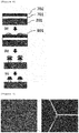
- FIG. 6 illustrates a cross-section of the forming of the auxiliary electrode formed of two or more metal layers according to the exemplary embodiment of the present specification. Specifically, FIG. 6 illustrates a process of forming a first metal layer 701 and a second metal layer 702 on the first electrode 201, (a) forming an etching protection layer 801 on the second metal layer 702, (b) performing etching by using an etchant, and (c) stripping the etching protection layer 801.
- the method of manufacturing the organic solar cell may include preparing a substrate, forming an anode on the substrate, forming a hole transport layer on the anode, forming a photoactive layer on the hole transport layer, forming an electron transport layer on the photoactive layer, and forming a cathode on the electron transport layer.
- the method of manufacturing the organic solar cell may include preparing a substrate, forming a cathode on an upper portion of the substrate, forming an electron transport layer on the cathode, forming a photoactive layer on the electron transport layer, forming a hole transport layer on the photoactive layer, and forming an anode on the hole transport layer.
- the organic solar cell of the present specification may be manufactured by sequentially laminating the anode, the photoactive layer, and the cathode on the substrate.
- the organic solar cell according to the present invention may be manufactured by forming the anode by depositing a metal or a metal oxide having conductivity or an alloy thereof on the substrate by using a PVD (physical vapor deposition) method such as sputtering or e-beam evaporation, forming the organic material layer thereon by a vacuum deposition or solution coating method, and depositing a material capable of being used as a cathode thereon.
- PVD physical vapor deposition
- the organic material layer of the individual layer may be manufactured using various unimolecular or polymer materials by not a deposition method but a solvent process, for example, a method such as roll to roll, spin coating, dip coating, casting, roll court, flow coating, doctor blading, screen printing, inkjet printing, gravure printing, offset printing, spray coating, or a heat transferring method.
- a solvent process for example, a method such as roll to roll, spin coating, dip coating, casting, roll court, flow coating, doctor blading, screen printing, inkjet printing, gravure printing, offset printing, spray coating, or a heat transferring method.
- the organic material layer of the individual layer may be manufactured by a method such as a dry film forming method such as vacuum deposition, sputtering, plasma, and ion plating.
- an anode deposition step may be included.
- a photoactive layer lamination step may be included.
- a photoactive layer alignment step may be included.
- a photoactive layer heat treatment step may be included.
- the photoactive layer may be disposed in a complex thin film structure deposited by spraying a solution where an electron donor material and an electron acceptor material are mixed on an upper side of the anode, that is, bulk heterojunction.
- a mixture solution where a complex polymer material is dissolved in an organic solvent may be used.
- the hexagonal mesh pattern having the line width of about 7 ⁇ m was formed by the photolithography method using the novolac-based positive photoresist (PR). Thereafter, after etching was performed by using the phosphoric acid/nitric acid/acetic acid-based etchant at 45°C for 9 seconds, the shape was observed by the optical microscope, and the cross-section was observed by the scanning electron microscope (SEM). Thereafter, the novolac photoresist was removed by using the organic amine-based stripper to manufacture the transparent electrode including the ITO/inverse taper metal auxiliary electrode.
- PR novolac-based positive photoresist
- FIG. 7 is an optical microscope picture immediately after PR patterning is performed by the method of Preparation Example 1
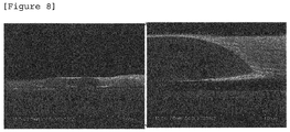
- FIG. 8 is a SEM cross-sectional picture immediately after PR patterning and Cu/Al etching are performed by the method of Preparation Example 1.
- ITO is not etched but remains and the etching rate of Cu is faster than that of Al in the same etchant
- Al is positioned at the lower portion of PR while about 7 ⁇ m that is the line width of PR is maintained, but since the etching rate of Cu is fast, additional etching occurs at the lower portion of Al, and thus the line width becomes very narrow.
- the PEDOT:PSS solution was applied, and heat treatment was then performed at 140°C for 15 minutes.
- the solution of P3HT and PCBM mixed at the ratio of 1 : 0.7 was applied on PEDOT:PSS to form the photoactive layer of about 220 nm
- the Al electrode was deposited on the photoactive layer under 1 ⁇ 10 -7 torr, and then subjected to heat treatment at 150°C for 10 minutes to manufacture the organic solar cell.
- the organic solar cell was manufactured by the same method as Example 1 while the auxiliary electrode was not formed.
- the organic solar cell was manufactured by the same method as Example 1, except that the metal electrode where the ratio of the line widths of the lower surface and the upper surface of the auxiliary electrode was 1 : 1 was provided.
- V oc means an open circuit voltage
- J sc means a short-circuit current
- FF means a fill factor
- PCE means energy conversion efficiency.
- the open-circuit voltage and the short-circuit current are respectively intercepts of X and Y axes in fourth quadrants of a voltage-current density curve, and as these two values are increased, efficiency of the solar cell is preferably increased.
- the fill factor is a value obtained by dividing an area of a rectangle that may be drawn in the curve by the product of the short-circuit current and the open circuit voltage. If these three values are divided by the intensity of radiated light, energy conversion efficiency may be obtained, and the higher the value is, the better the efficiency is.
- the organic solar cell was manufactured by the same method as Example 1, and while the area of the photoactive layer was increased, properties of the reduction in resistance and the increase in light absorption caused by the auxiliary electrode where the ratio of the line widths of the lower surface and the upper surface of the auxiliary electrode was 1 : 2 were observed.
- Example 3 Area of photoactive layer (mm 2 ) V oc (V) J sc (mA/cm 2 ) FF PCE (%) 43.6 0.62 10.12 0.57 3.60 194 0.62 8.79 0.45 2.45 287 0.62 7.4 0.43 1.97
- the organic solar cell was manufactured by the same method as Comparative Example 1, and while the area of the photoactive layer was increased, properties of the reduction in resistance and the increase in light absorption of the device not having the auxiliary electrode were observed.
- the organic solar cell was manufactured by the same method as Comparative Example 2, and while the area of the photoactive layer was increased, properties of the reduction in resistance and the increase in light absorption caused by the auxiliary electrode where the ratio of the line widths of the lower surface and the upper surface of the auxiliary electrode was 1 : 1 were observed.
- Comparative Example 4 Area of photoactive layer (mm 2 ) V oc (V) J sc (mA/cm 2 ) FF PCE (%) 43.6 0.62 9.22 0.56 3.20 194 0.62 8.05 0.40 2.10 287 0.62 7.01 0.37 1.61
Landscapes
- Physics & Mathematics (AREA)
- Electromagnetism (AREA)
- Photovoltaic Devices (AREA)
Claims (13)
- Organische Solarzelle, umfassend:eine erste Elektrode (201);eine zweite Elektrode (601), die so angeordnet ist, dass sie der ersten Elektrode gegenüber liegt;eine organische Materialschicht aus einer oder mehreren Schichten, die eine photoaktive Schicht (501) enthalten, die zwischen der ersten Elektrode und der zweiten Elektrode angeordnet ist; undeine Hilfselektrode (301), die so angeordnet ist, dass sie mit der ersten Elektrode in Kontakt kommt,wobei das einfallende Licht die erste Elektrode erreicht unddadurch gekennzeichnet, dassin der Hilfselektrode eine Fläche einer Oberfläche, die mit der ersten Elektrode in Kontakt kommt, kleiner als eine Fläche einer gegenüberliegenden Oberfläche davon ist.
- Organische Solarzelle gemäß Anspruch 1, wobei die erste Elektrode, die das einfallende Licht erreicht, eine transparente Elektrode ist.
- Organische Solarzelle gemäß Anspruch 1, wobei ein vertikaler Querschnitt der Hilfselektrode eine trapezförmige Form aufweist.
- Organische Solarzelle gemäß Anspruch 1, wobei in der Hilfselektrode ein Verhältnis von Linienbreiten einer oberen Oberfläche und einer unteren Oberfläche 1:1,3 bis 1:3 oder 1,3:1 bis 3:1 beträgt.
- Organische Solarzelle gemäß Anspruch 1, wobei die Hilfselektrode eine Metallelektrode ist.
- Organische Solarzelle gemäß Anspruch 1, wobei die Hilfselektrode in einer Maschenstruktur angeordnet ist.
- Organische Solarzelle gemäß Anspruch 1, wobei die Hilfselektrode aus zwei oder mehr Schichten gebildet ist.
- Organische Solarzelle gemäß Anspruch 7, wobei in einzelnen Schichten der Hilfselektrode eine Fläche einer Oberfläche nahe einer ersten Elektrode, die das einfallende Licht erreicht, kleiner als eine Fläche einer gegenüberliegenden Oberfläche davon ist.
- Organische Solarzelle gemäß Anspruch 7, wobei in der Hilfselektrode aus zwei oder mehr Schichten eine Fläche einer Oberfläche, die einer ersten Elektrode, die ein einfallendes Licht erreicht, am nächsten liegt, kleiner als eine Fläche einer gegenüberliegenden Oberfläche davon, die am weitesten von der ersten oder zweiten Elektrode entfernt ist, ist.
- Organische Solarzelle gemäß Anspruch 7, wobei einzelne Schichten der Hilfselektrode aus Materialien bestehen, die sich voneinander unterscheiden.
- Organische Solarzelle gemäß Anspruch 7, wobei Formen der vertikalen Querschnitte einzelner Schichten der Hilfselektrode jeweils unabhängig voneinander ein Quadrat, ein Rechteck oder ein Trapez sind.
- Organische Solarzelle gemäß Anspruch 1, wobei die photoaktive Schicht eine Zweischichtstruktur aufweist, die eine organische Materialschicht vom n-Typ und eine organische Materialschicht vom p-Typ enthält.
- Organische Solarzelle gemäß Anspruch 1, wobei die photoaktive Schicht eine Bulk-Heteroübergangsstruktur aufweist, die ein Elektronendonormaterial und ein Elektronenakzeptormaterial enthält.
Applications Claiming Priority (2)
| Application Number | Priority Date | Filing Date | Title |
|---|---|---|---|
| KR20130068553 | 2013-06-14 | ||
| PCT/KR2014/005225 WO2014200312A1 (ko) | 2013-06-14 | 2014-06-13 | 유기태양전지 및 이의 제조방법 |
Publications (3)
| Publication Number | Publication Date |
|---|---|
| EP2999017A1 EP2999017A1 (de) | 2016-03-23 |
| EP2999017A4 EP2999017A4 (de) | 2016-12-28 |
| EP2999017B1 true EP2999017B1 (de) | 2019-11-06 |
Family
ID=52022516
Family Applications (1)
| Application Number | Title | Priority Date | Filing Date |
|---|---|---|---|
| EP14810301.3A Active EP2999017B1 (de) | 2013-06-14 | 2014-06-13 | Organische fotovoltaische zelle |
Country Status (6)
| Country | Link |
|---|---|
| US (1) | US10446772B2 (de) |
| EP (1) | EP2999017B1 (de) |
| JP (1) | JP6162891B2 (de) |
| KR (1) | KR101557587B1 (de) |
| CN (1) | CN105393376B (de) |
| WO (1) | WO2014200312A1 (de) |
Families Citing this family (15)
| Publication number | Priority date | Publication date | Assignee | Title |
|---|---|---|---|---|
| KR101539959B1 (ko) * | 2015-01-06 | 2015-07-30 | 성안기계 (주) | 유기 태양 전지 제조 방법 |
| KR102278243B1 (ko) * | 2015-02-25 | 2021-07-19 | 한국전자통신연구원 | 전기변색 소자 |
| KR101702239B1 (ko) * | 2015-10-30 | 2017-02-02 | 재단법인 멀티스케일 에너지시스템 연구단 | 페로브스카이트 태양전지의 재생방법 |
| KR101928932B1 (ko) * | 2015-12-07 | 2018-12-13 | 주식회사 엘지화학 | 중합체 및 이를 포함하는 유기 태양 전지 |
| KR102137547B1 (ko) * | 2016-08-12 | 2020-07-24 | 삼성에스디아이 주식회사 | 태양전지용 전면 전극 및 이를 포함하는 태양전지 |
| KR20190020978A (ko) | 2017-08-22 | 2019-03-05 | 코오롱인더스트리 주식회사 | 유기 태양전지 |
| CN110637345B (zh) * | 2017-09-19 | 2021-10-29 | 株式会社Lg化学 | 用于透明发光器件显示器的电极基底及其制造方法 |
| KR102235223B1 (ko) | 2017-11-28 | 2021-04-02 | 주식회사 엘지화학 | 광활성층 및 이를 포함하는 유기태양전지 |
| CN108400241A (zh) * | 2018-01-18 | 2018-08-14 | 华北电力大学 | 用8-羟基喹啉钛作电子传输层的聚合物太阳能电池及其制备方法 |
| CN108899424B (zh) * | 2018-06-28 | 2023-05-19 | 国家纳米科学中心 | 一种有机光伏电池及其制备方法 |
| CN109786559A (zh) * | 2018-12-28 | 2019-05-21 | 浙江清华柔性电子技术研究院 | 光伏组件及智能发电窗户 |
| TWI732444B (zh) * | 2020-02-05 | 2021-07-01 | 凌巨科技股份有限公司 | 太陽能電池緩坡結構及其製造方法 |
| KR102724540B1 (ko) | 2022-05-11 | 2024-10-30 | 성균관대학교산학협력단 | 페로브스카이트 태양전지 모듈의 분리 용액을 재활용하는 방법 및 이를 이용한 페로브스카이트 태양전지 |
| KR102730817B1 (ko) * | 2022-07-25 | 2024-11-14 | 전북대학교산학협력단 | 반투명 페로브스카이트 태양 전지의 제조 방법 및 반투명 페로브스카이트 태양 전지 |
| CN115623795A (zh) * | 2022-09-29 | 2023-01-17 | 苏州清越光电科技股份有限公司 | 柔性钙钛矿太阳能电池及其制备工艺 |
Family Cites Families (24)
| Publication number | Priority date | Publication date | Assignee | Title |
|---|---|---|---|---|
| JP2002523036A (ja) * | 1998-08-25 | 2002-07-30 | レキシジェン ファーマシューティカルズ コーポレイション | イムノフュージンとしての新脈管形成インヒビターの発現および輸送 |
| JP4984197B2 (ja) * | 1999-02-18 | 2012-07-25 | 大日本印刷株式会社 | 透明フィルム型太陽電池モジュール |
| JP4776748B2 (ja) * | 1999-12-22 | 2011-09-21 | 株式会社半導体エネルギー研究所 | 太陽電池 |
| KR100689229B1 (ko) * | 2002-10-03 | 2007-03-02 | 가부시키가이샤후지쿠라 | 전극 기판, 광전변환 소자, 도전성 글래스 기판 및 그 제조방법, 및 색소증감 태양전지 |
| KR101036539B1 (ko) * | 2003-03-24 | 2011-05-24 | 코나르카 테크놀로지, 인코포레이티드 | 메쉬 전극을 갖는 광전지 |
| US7638807B2 (en) * | 2003-10-28 | 2009-12-29 | Sumitomo Metal Mining Co., Ltd. | Transparent conductive multi-layer structure, process for its manufacture and device making use of transparent conductive multi-layer structure |
| TWM266605U (en) * | 2004-07-07 | 2005-06-01 | Kingconn Technology Co Ltd | Dual purpose memory card connection socket |
| DE102006023257B4 (de) * | 2005-07-09 | 2011-05-12 | Atmel Automotive Gmbh | Vorrichtung zum Heissproben von integrierten Halbleiterschaltkreisen auf Wafern |
| US7314773B2 (en) | 2005-08-17 | 2008-01-01 | The Trustees Of Princeton University | Low resistance thin film organic solar cell electrodes |
| KR100764362B1 (ko) * | 2005-11-01 | 2007-10-08 | 삼성전자주식회사 | 태양전지용 투명 전극, 그의 제조방법 및 그를 포함하는반도체 전극 |
| US20080216894A1 (en) * | 2007-01-08 | 2008-09-11 | Plextronics, Inc. | Quantum dot photovoltaic device |
| KR20110079878A (ko) | 2008-08-12 | 2011-07-11 | 다이솔 엘티디 | 플렉시블 광전 표시 소자에서 사용되는 집전체 시스템 및 그 제조 방법 |
| DE102008045948A1 (de) * | 2008-09-04 | 2010-03-11 | Osram Opto Semiconductors Gmbh | Verfahren zur Herstellung eines organischen strahlungsemittierenden Bauelements und organisches strahlungsemittierendes Bauelement |
| JP2010141250A (ja) * | 2008-12-15 | 2010-06-24 | Dainippon Printing Co Ltd | 有機薄膜太陽電池およびその製造方法 |
| JP5326731B2 (ja) | 2009-03-26 | 2013-10-30 | 大日本印刷株式会社 | 有機薄膜太陽電池 |
| JP2011159934A (ja) * | 2010-02-04 | 2011-08-18 | Mitsubishi Chemicals Corp | 有機太陽電池セル、太陽電池モジュール及び有機太陽電池セルの製造方法 |
| JP2011222819A (ja) | 2010-04-12 | 2011-11-04 | Mitsubishi Chemicals Corp | 太陽電池 |
| KR101152544B1 (ko) * | 2010-07-29 | 2012-06-01 | 삼성에스디아이 주식회사 | 광전 변환 소자용 전극, 이의 제조 방법 및 이를 포함하는 광전 변환 소자 |
| JP2012057011A (ja) * | 2010-09-07 | 2012-03-22 | Kyocera Chemical Corp | 部分多孔質ポリマー粒子の製造方法及び部分多孔質ポリマー粒子 |
| JP5421218B2 (ja) * | 2010-10-26 | 2014-02-19 | 出光興産株式会社 | 光電変換装置、及び光電変換装置の製造方法 |
| JP2012146420A (ja) * | 2011-01-07 | 2012-08-02 | Toppan Printing Co Ltd | 色素増感太陽電池および色素増感太陽電池の製造方法 |
| JP2013016669A (ja) * | 2011-07-05 | 2013-01-24 | Fujifilm Corp | 光電変換素子の製造方法 |
| CN102637826A (zh) | 2012-05-04 | 2012-08-15 | 中国科学院长春光学精密机械与物理研究所 | 一种大面积有机太阳能电池结构及其制备方法 |
| CN103078057B (zh) * | 2013-01-29 | 2016-01-20 | 苏州大学 | 有机太阳能电池及其制作方法 |
-
2014
- 2014-06-13 EP EP14810301.3A patent/EP2999017B1/de active Active
- 2014-06-13 US US14/897,919 patent/US10446772B2/en active Active
- 2014-06-13 CN CN201480033479.7A patent/CN105393376B/zh active Active
- 2014-06-13 KR KR1020140072465A patent/KR101557587B1/ko active Active
- 2014-06-13 JP JP2016519452A patent/JP6162891B2/ja active Active
- 2014-06-13 WO PCT/KR2014/005225 patent/WO2014200312A1/ko not_active Ceased
Non-Patent Citations (1)
| Title |
|---|
| None * |
Also Published As
| Publication number | Publication date |
|---|---|
| KR101557587B1 (ko) | 2015-10-05 |
| CN105393376B (zh) | 2017-11-17 |
| CN105393376A (zh) | 2016-03-09 |
| EP2999017A1 (de) | 2016-03-23 |
| KR20140146010A (ko) | 2014-12-24 |
| US10446772B2 (en) | 2019-10-15 |
| WO2014200312A1 (ko) | 2014-12-18 |
| JP6162891B2 (ja) | 2017-07-12 |
| US20160141536A1 (en) | 2016-05-19 |
| EP2999017A4 (de) | 2016-12-28 |
| JP2016521921A (ja) | 2016-07-25 |
Similar Documents
| Publication | Publication Date | Title |
|---|---|---|
| US10446772B2 (en) | Organic solar cell and method of manufacturing the same | |
| JP5225305B2 (ja) | 有機薄膜太陽電池およびその製造方法 | |
| CN102217112A (zh) | 有机薄膜太阳能电池及其制造方法 | |
| CN102306707A (zh) | 一种基于胶体量子点及石墨烯为光电极的光电探测器及其制备方法 | |
| KR20110133717A (ko) | 유기 태양 전지 및 그 제조 방법 | |
| KR20120096046A (ko) | 유기 태양전지 | |
| WO2011052582A1 (ja) | 有機薄膜太陽電池モジュールの製造方法 | |
| JP2016058455A (ja) | 光電変換素子、光電変換素子の配線基板、光電変換素子の製造方法、および光電変換構造体 | |
| CN108864414A (zh) | 阴极界面修饰材料、太阳能电池及其制作方法与应用 | |
| JP5444743B2 (ja) | 有機光電変換素子 | |
| CN102280590B (zh) | 一种基于胶体量子点及石墨烯为光阳极的太阳电池及其制备方法 | |
| JP2007005620A (ja) | 有機薄膜太陽電池 | |
| JP5439418B2 (ja) | 有機薄膜太陽電池モジュール及びサブモジュール | |
| US20110233533A1 (en) | Organic thin film device | |
| CN113826230A (zh) | 透明电极和透明电极的制造方法,以及具备透明电极的光电转换元件 | |
| JP2013026483A (ja) | 有機光電変換素子、有機光電変換素子の製造方法及び太陽電池 | |
| CN102132437A (zh) | 有机光电转换元件及其制造方法 | |
| CN102201536B (zh) | 一种有机薄膜太阳能电池及其制备方法 | |
| CN106233485A (zh) | 堆叠型有机太阳能电池 | |
| CN108140738A (zh) | 有机太阳能电池及其制造方法 | |
| JP2016082242A (ja) | 有機光電変換素子およびその製造方法 | |
| JP5715796B2 (ja) | 有機光電変換素子の製造方法 | |
| JP5304448B2 (ja) | 有機光電変換素子 | |
| JP6076392B2 (ja) | 太陽電池モジュールおよびその製造方法 | |
| CN104241532A (zh) | 一种有机光伏电池及制备方法 |
Legal Events
| Date | Code | Title | Description |
|---|---|---|---|
| PUAI | Public reference made under article 153(3) epc to a published international application that has entered the european phase |
Free format text: ORIGINAL CODE: 0009012 |
|
| 17P | Request for examination filed |
Effective date: 20151209 |
|
| AK | Designated contracting states |
Kind code of ref document: A1 Designated state(s): AL AT BE BG CH CY CZ DE DK EE ES FI FR GB GR HR HU IE IS IT LI LT LU LV MC MK MT NL NO PL PT RO RS SE SI SK SM TR |
|
| AX | Request for extension of the european patent |
Extension state: BA ME |
|
| DAX | Request for extension of the european patent (deleted) | ||
| REG | Reference to a national code |
Ref country code: DE Ref legal event code: R079 Ref document number: 602014056420 Country of ref document: DE Free format text: PREVIOUS MAIN CLASS: H01L0051420000 Ipc: H01L0051440000 |
|
| A4 | Supplementary search report drawn up and despatched |
Effective date: 20161130 |
|
| RIC1 | Information provided on ipc code assigned before grant |
Ipc: H01L 51/44 20060101AFI20161124BHEP Ipc: H01L 51/48 20060101ALI20161124BHEP |
|
| GRAP | Despatch of communication of intention to grant a patent |
Free format text: ORIGINAL CODE: EPIDOSNIGR1 |
|
| STAA | Information on the status of an ep patent application or granted ep patent |
Free format text: STATUS: GRANT OF PATENT IS INTENDED |
|
| INTG | Intention to grant announced |
Effective date: 20190726 |
|
| GRAS | Grant fee paid |
Free format text: ORIGINAL CODE: EPIDOSNIGR3 |
|
| GRAA | (expected) grant |
Free format text: ORIGINAL CODE: 0009210 |
|
| STAA | Information on the status of an ep patent application or granted ep patent |
Free format text: STATUS: THE PATENT HAS BEEN GRANTED |
|
| AK | Designated contracting states |
Kind code of ref document: B1 Designated state(s): AL AT BE BG CH CY CZ DE DK EE ES FI FR GB GR HR HU IE IS IT LI LT LU LV MC MK MT NL NO PL PT RO RS SE SI SK SM TR |
|
| REG | Reference to a national code |
Ref country code: GB Ref legal event code: FG4D |
|
| REG | Reference to a national code |
Ref country code: CH Ref legal event code: EP Ref country code: AT Ref legal event code: REF Ref document number: 1200005 Country of ref document: AT Kind code of ref document: T Effective date: 20191115 |
|
| REG | Reference to a national code |
Ref country code: IE Ref legal event code: FG4D |
|
| REG | Reference to a national code |
Ref country code: DE Ref legal event code: R096 Ref document number: 602014056420 Country of ref document: DE |
|
| REG | Reference to a national code |
Ref country code: NL Ref legal event code: MP Effective date: 20191106 |
|
| REG | Reference to a national code |
Ref country code: LT Ref legal event code: MG4D |
|
| PG25 | Lapsed in a contracting state [announced via postgrant information from national office to epo] |
Ref country code: LV Free format text: LAPSE BECAUSE OF FAILURE TO SUBMIT A TRANSLATION OF THE DESCRIPTION OR TO PAY THE FEE WITHIN THE PRESCRIBED TIME-LIMIT Effective date: 20191106 Ref country code: SE Free format text: LAPSE BECAUSE OF FAILURE TO SUBMIT A TRANSLATION OF THE DESCRIPTION OR TO PAY THE FEE WITHIN THE PRESCRIBED TIME-LIMIT Effective date: 20191106 Ref country code: NL Free format text: LAPSE BECAUSE OF FAILURE TO SUBMIT A TRANSLATION OF THE DESCRIPTION OR TO PAY THE FEE WITHIN THE PRESCRIBED TIME-LIMIT Effective date: 20191106 Ref country code: FI Free format text: LAPSE BECAUSE OF FAILURE TO SUBMIT A TRANSLATION OF THE DESCRIPTION OR TO PAY THE FEE WITHIN THE PRESCRIBED TIME-LIMIT Effective date: 20191106 Ref country code: BG Free format text: LAPSE BECAUSE OF FAILURE TO SUBMIT A TRANSLATION OF THE DESCRIPTION OR TO PAY THE FEE WITHIN THE PRESCRIBED TIME-LIMIT Effective date: 20200206 Ref country code: PT Free format text: LAPSE BECAUSE OF FAILURE TO SUBMIT A TRANSLATION OF THE DESCRIPTION OR TO PAY THE FEE WITHIN THE PRESCRIBED TIME-LIMIT Effective date: 20200306 Ref country code: NO Free format text: LAPSE BECAUSE OF FAILURE TO SUBMIT A TRANSLATION OF THE DESCRIPTION OR TO PAY THE FEE WITHIN THE PRESCRIBED TIME-LIMIT Effective date: 20200206 Ref country code: LT Free format text: LAPSE BECAUSE OF FAILURE TO SUBMIT A TRANSLATION OF THE DESCRIPTION OR TO PAY THE FEE WITHIN THE PRESCRIBED TIME-LIMIT Effective date: 20191106 Ref country code: PL Free format text: LAPSE BECAUSE OF FAILURE TO SUBMIT A TRANSLATION OF THE DESCRIPTION OR TO PAY THE FEE WITHIN THE PRESCRIBED TIME-LIMIT Effective date: 20191106 Ref country code: GR Free format text: LAPSE BECAUSE OF FAILURE TO SUBMIT A TRANSLATION OF THE DESCRIPTION OR TO PAY THE FEE WITHIN THE PRESCRIBED TIME-LIMIT Effective date: 20200207 |
|
| PG25 | Lapsed in a contracting state [announced via postgrant information from national office to epo] |
Ref country code: RS Free format text: LAPSE BECAUSE OF FAILURE TO SUBMIT A TRANSLATION OF THE DESCRIPTION OR TO PAY THE FEE WITHIN THE PRESCRIBED TIME-LIMIT Effective date: 20191106 Ref country code: HR Free format text: LAPSE BECAUSE OF FAILURE TO SUBMIT A TRANSLATION OF THE DESCRIPTION OR TO PAY THE FEE WITHIN THE PRESCRIBED TIME-LIMIT Effective date: 20191106 Ref country code: IS Free format text: LAPSE BECAUSE OF FAILURE TO SUBMIT A TRANSLATION OF THE DESCRIPTION OR TO PAY THE FEE WITHIN THE PRESCRIBED TIME-LIMIT Effective date: 20200306 |
|
| PG25 | Lapsed in a contracting state [announced via postgrant information from national office to epo] |
Ref country code: AL Free format text: LAPSE BECAUSE OF FAILURE TO SUBMIT A TRANSLATION OF THE DESCRIPTION OR TO PAY THE FEE WITHIN THE PRESCRIBED TIME-LIMIT Effective date: 20191106 |
|
| PG25 | Lapsed in a contracting state [announced via postgrant information from national office to epo] |
Ref country code: CZ Free format text: LAPSE BECAUSE OF FAILURE TO SUBMIT A TRANSLATION OF THE DESCRIPTION OR TO PAY THE FEE WITHIN THE PRESCRIBED TIME-LIMIT Effective date: 20191106 Ref country code: RO Free format text: LAPSE BECAUSE OF FAILURE TO SUBMIT A TRANSLATION OF THE DESCRIPTION OR TO PAY THE FEE WITHIN THE PRESCRIBED TIME-LIMIT Effective date: 20191106 Ref country code: ES Free format text: LAPSE BECAUSE OF FAILURE TO SUBMIT A TRANSLATION OF THE DESCRIPTION OR TO PAY THE FEE WITHIN THE PRESCRIBED TIME-LIMIT Effective date: 20191106 Ref country code: DK Free format text: LAPSE BECAUSE OF FAILURE TO SUBMIT A TRANSLATION OF THE DESCRIPTION OR TO PAY THE FEE WITHIN THE PRESCRIBED TIME-LIMIT Effective date: 20191106 Ref country code: EE Free format text: LAPSE BECAUSE OF FAILURE TO SUBMIT A TRANSLATION OF THE DESCRIPTION OR TO PAY THE FEE WITHIN THE PRESCRIBED TIME-LIMIT Effective date: 20191106 |
|
| REG | Reference to a national code |
Ref country code: DE Ref legal event code: R097 Ref document number: 602014056420 Country of ref document: DE |
|
| REG | Reference to a national code |
Ref country code: AT Ref legal event code: MK05 Ref document number: 1200005 Country of ref document: AT Kind code of ref document: T Effective date: 20191106 |
|
| PG25 | Lapsed in a contracting state [announced via postgrant information from national office to epo] |
Ref country code: SK Free format text: LAPSE BECAUSE OF FAILURE TO SUBMIT A TRANSLATION OF THE DESCRIPTION OR TO PAY THE FEE WITHIN THE PRESCRIBED TIME-LIMIT Effective date: 20191106 Ref country code: SM Free format text: LAPSE BECAUSE OF FAILURE TO SUBMIT A TRANSLATION OF THE DESCRIPTION OR TO PAY THE FEE WITHIN THE PRESCRIBED TIME-LIMIT Effective date: 20191106 |
|
| PLBE | No opposition filed within time limit |
Free format text: ORIGINAL CODE: 0009261 |
|
| STAA | Information on the status of an ep patent application or granted ep patent |
Free format text: STATUS: NO OPPOSITION FILED WITHIN TIME LIMIT |
|
| 26N | No opposition filed |
Effective date: 20200807 |
|
| PG25 | Lapsed in a contracting state [announced via postgrant information from national office to epo] |
Ref country code: SI Free format text: LAPSE BECAUSE OF FAILURE TO SUBMIT A TRANSLATION OF THE DESCRIPTION OR TO PAY THE FEE WITHIN THE PRESCRIBED TIME-LIMIT Effective date: 20191106 Ref country code: AT Free format text: LAPSE BECAUSE OF FAILURE TO SUBMIT A TRANSLATION OF THE DESCRIPTION OR TO PAY THE FEE WITHIN THE PRESCRIBED TIME-LIMIT Effective date: 20191106 |
|
| PG25 | Lapsed in a contracting state [announced via postgrant information from national office to epo] |
Ref country code: IT Free format text: LAPSE BECAUSE OF FAILURE TO SUBMIT A TRANSLATION OF THE DESCRIPTION OR TO PAY THE FEE WITHIN THE PRESCRIBED TIME-LIMIT Effective date: 20191106 Ref country code: MC Free format text: LAPSE BECAUSE OF FAILURE TO SUBMIT A TRANSLATION OF THE DESCRIPTION OR TO PAY THE FEE WITHIN THE PRESCRIBED TIME-LIMIT Effective date: 20191106 |
|
| REG | Reference to a national code |
Ref country code: CH Ref legal event code: PL |
|
| PG25 | Lapsed in a contracting state [announced via postgrant information from national office to epo] |
Ref country code: LU Free format text: LAPSE BECAUSE OF NON-PAYMENT OF DUE FEES Effective date: 20200613 |
|
| REG | Reference to a national code |
Ref country code: BE Ref legal event code: MM Effective date: 20200630 |
|
| PG25 | Lapsed in a contracting state [announced via postgrant information from national office to epo] |
Ref country code: LI Free format text: LAPSE BECAUSE OF NON-PAYMENT OF DUE FEES Effective date: 20200630 Ref country code: IE Free format text: LAPSE BECAUSE OF NON-PAYMENT OF DUE FEES Effective date: 20200613 Ref country code: CH Free format text: LAPSE BECAUSE OF NON-PAYMENT OF DUE FEES Effective date: 20200630 |
|
| PG25 | Lapsed in a contracting state [announced via postgrant information from national office to epo] |
Ref country code: BE Free format text: LAPSE BECAUSE OF NON-PAYMENT OF DUE FEES Effective date: 20200630 |
|
| PG25 | Lapsed in a contracting state [announced via postgrant information from national office to epo] |
Ref country code: TR Free format text: LAPSE BECAUSE OF FAILURE TO SUBMIT A TRANSLATION OF THE DESCRIPTION OR TO PAY THE FEE WITHIN THE PRESCRIBED TIME-LIMIT Effective date: 20191106 Ref country code: MT Free format text: LAPSE BECAUSE OF FAILURE TO SUBMIT A TRANSLATION OF THE DESCRIPTION OR TO PAY THE FEE WITHIN THE PRESCRIBED TIME-LIMIT Effective date: 20191106 Ref country code: CY Free format text: LAPSE BECAUSE OF FAILURE TO SUBMIT A TRANSLATION OF THE DESCRIPTION OR TO PAY THE FEE WITHIN THE PRESCRIBED TIME-LIMIT Effective date: 20191106 |
|
| PG25 | Lapsed in a contracting state [announced via postgrant information from national office to epo] |
Ref country code: MK Free format text: LAPSE BECAUSE OF FAILURE TO SUBMIT A TRANSLATION OF THE DESCRIPTION OR TO PAY THE FEE WITHIN THE PRESCRIBED TIME-LIMIT Effective date: 20191106 |
|
| REG | Reference to a national code |
Ref country code: DE Ref legal event code: R079 Ref document number: 602014056420 Country of ref document: DE Free format text: PREVIOUS MAIN CLASS: H01L0051440000 Ipc: H10K0030800000 |
|
| PGFP | Annual fee paid to national office [announced via postgrant information from national office to epo] |
Ref country code: GB Payment date: 20260526 Year of fee payment: 13 |
|
| PGFP | Annual fee paid to national office [announced via postgrant information from national office to epo] |
Ref country code: DE Payment date: 20260520 Year of fee payment: 13 |
|
| PGFP | Annual fee paid to national office [announced via postgrant information from national office to epo] |
Ref country code: FR Payment date: 20260527 Year of fee payment: 13 |