EP2997459B1 - System and method for high performance and low cost flash translation layer - Google Patents
System and method for high performance and low cost flash translation layer Download PDFInfo
- Publication number
- EP2997459B1 EP2997459B1 EP14730327.5A EP14730327A EP2997459B1 EP 2997459 B1 EP2997459 B1 EP 2997459B1 EP 14730327 A EP14730327 A EP 14730327A EP 2997459 B1 EP2997459 B1 EP 2997459B1
- Authority
- EP
- European Patent Office
- Prior art keywords
- flash memory
- memory device
- host device
- copy
- ftl
- Prior art date
- Legal status (The legal status is an assumption and is not a legal conclusion. Google has not performed a legal analysis and makes no representation as to the accuracy of the status listed.)
- Not-in-force
Links
Images


Classifications
-
- G—PHYSICS
- G06—COMPUTING; CALCULATING OR COUNTING
- G06F—ELECTRIC DIGITAL DATA PROCESSING
- G06F12/00—Accessing, addressing or allocating within memory systems or architectures
- G06F12/02—Addressing or allocation; Relocation
- G06F12/0223—User address space allocation, e.g. contiguous or non contiguous base addressing
- G06F12/023—Free address space management
- G06F12/0238—Memory management in non-volatile memory, e.g. resistive RAM or ferroelectric memory
- G06F12/0246—Memory management in non-volatile memory, e.g. resistive RAM or ferroelectric memory in block erasable memory, e.g. flash memory
-
- G—PHYSICS
- G06—COMPUTING; CALCULATING OR COUNTING
- G06F—ELECTRIC DIGITAL DATA PROCESSING
- G06F2212/00—Indexing scheme relating to accessing, addressing or allocation within memory systems or architectures
- G06F2212/72—Details relating to flash memory management
- G06F2212/7201—Logical to physical mapping or translation of blocks or pages
-
- G—PHYSICS
- G06—COMPUTING; CALCULATING OR COUNTING
- G06F—ELECTRIC DIGITAL DATA PROCESSING
- G06F2212/00—Indexing scheme relating to accessing, addressing or allocation within memory systems or architectures
- G06F2212/72—Details relating to flash memory management
- G06F2212/7203—Temporary buffering, e.g. using volatile buffer or dedicated buffer blocks
Definitions
- US 2012/179859 A1 discloses a nonvolatile memory apparatus including: a memory controller coupled and a memory area comprising a plurality of memory blocks controlled by the memory controller.
- the memory controller sets a plurality of physical blocks corresponding to the plurality of memory blocks, and sets a plurality of logical blocks which are mapping targets of the physical blocks such that a size of the logical blocks and a size of the physical blocks are asymmetrical.
- accessing the copy of the FTL table may further include bus mastering, by the flash memory device, a communication bus communicatively connecting the flash memory device and the volatile memory of the host device.
- accessing the copy of the FTL table may include receiving by the flash memory device a write operation request for a logical address from the host device, initiating the write operation by the flash memory device, writing data to a physical address of a memory of the flash memory device by the flash memory device, writing to the copy of the FTL table, by the flash memory device, to update the copy of the FTL table to correspond with changes made to the memory of the flash memory device when the data was written, and sending a notification of completion of the write operation to the host device by the flash memory device.
- An aspect method may further include reading at least a portion of the copy of the FTL table by the flash memory device, and determining the physical address corresponding to the logical address by the flash memory device.
- An aspect method may further include determining, by the host device, whether the flash memory device supports host caching of a copy of the FTL table in the volatile memory of the host device.
- An aspect method may further include receiving, in the host device, a notification of the completion of storing the copy of the FTL table from the flash memory device.
- Flash memory refers to an electronic non-volatile computer storage, or memory, that can be electrically erased and reprogrammed. Flash memory device architecture typically includes NAND and NOR types. Aspects herein generally relate to the NAND type architecture of flash memory devices. Flash memory may be used in main memory, memory cards, USB flash drives, solid-state drives, and similar products, for general storage and transfer of data. Examples of NAND flash memory devices include embedded MultiMediaCards (eMMC), universal flash storage (UFS), External Serial Advanced Technology Attachment (eSATA), ball grid array (BGA) SATA, Universal Serial Bus (USB) drive, Secure Digital (SD) card, universal subscriber identity module (USIM) card, and compact flash card.
- eMMC embedded MultiMediaCards
- UFS universal flash storage
- eSATA External Serial Advanced Technology Attachment
- BGA ball grid array
- USB Universal Serial Bus
- SD Secure Digital
- USB universal subscriber identity module
- USB universal subscriber identity module
- flash translation layer and "FTL” herein refer to a directory structure created to allow a controller of a flash memory device to convert requests for logical addresses into the physical addresses in the actual flash memory chips.
- the directory structure may comprise any of various data structures. For purposes of example, herein the FTL will be described as being in the form of tables.
- the read and/or write operation request may include logical addresses for where to read data from and/or write data to the flash memory device.
- the flash memory device may translate the logical address to a physical address of its own memory using the FTL tables. To do so, the flash memory device may use its direct memory access permissions to retrieve address mapping information from the copy of the FTL tables relating to the specified logical addresses in order to translate it to a corresponding physical address.
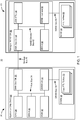
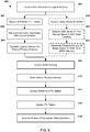
- the communication controllers 26, 32, 54, 60 may be configured to manage communication between multiple components of the FTL host caching system 10. Each communication controller 26, 32, 54, may specifically manage communication between a specific component and the other components.
- a direct memory access (DMA) bus controller 26 may be configured to manage communications between the CPU 24 and the DRAM 38, on one side of the DMA bus controller 26, and the microcontroller 56 on the other side.
- a DMA bus controller 54 may manage communication between the microcontroller 56, on one side of the DMA bus controller 54, and the CPU 24 on the other side.
- the DMA bus controller could be configured to manage address and data communications between the flash memory 64 and the CPU 24, if the CPU 24 was granted direct memory access to the flash memory 64.
- a DRAM controller 32 may be configured to manage communication between the DRAM 38 on one side, and the CPU 24 and the microcontroller 54 on the other side.
- the communication links 34, 36, 40, 62, 66 may provide a path for address and data communications between the various components of the FTL host caching system 10.
- the communication links 34, 36, 40, 62, 66 may be configured for internal communication between components of a single device, or external communication between a main device and a peripheral device.
- a host bus may provide the communication path between, for example, the CPU 24, the DMA bus controller 26, the SRAM 28, the ROM 30, and the DRAM controller 32.
- a DRAM bus 36 may provide the communication path between the DRAM 36 and other components, like the DRAM controller 32.
- a storage bus 40 may provide the communication path between the DMA bus controllers 26, 54.
- a flash memory device bus 62 may provide the communication path between the DMA bus controller 54, the microcontroller 56, the SRAM 58, and the flash memory interface 60.
- a flash memory bus 66 may provide the communication path between the flash memory 64 and other components, like the flash memory interface 60.
- the combination of some or all of these components forms a host device 20 and a flash memory device 50.
- the host device 20 and flash memory device 50 may be configured as separately housed devices with the ability to communicate over communication link 40.
- the host device 20 may be composed of the CPU 24, DMA bus controller 26, the SRAM 28, the ROM 30, the DRAM controller 32, the host bus 34, the DRAM bus 36, the DRAM 38, and a portion or all of the storage bus 40.
- the components may further be combined into an integrated circuit, such as a system on chip (SoC) 22.
- SoC 22 may include the CPU 24, DMA bus controller 26, the SRAM 28, the ROM 30, the DRAM controller 32, the host bus 34, and a portion or all of the DRAM bus 36 and the storage bus 40.
- the flash memory device 50 may further include a combination of components into an integrated circuit, such as a managed flash memory controller 52.
- Components of the managed flash memory controller 52 may include a portion or all of the storage bus 40 and the flash memory bus 66, the DMA bus controller 54, the microcontroller 56, the SRAM 58, the flash memory interface 60, and the flash memory device bus 62.
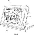
- FIG. 2 illustrates an example mobile device 200 suitable for use in the FTL host caching system 10.
- the mobile device 200 may include a processor 202 coupled to a touchscreen controller 204 and an internal memory 206.
- the internal memory 206 may be volatile or non-volatile memory, and may also be secure and/or encrypted memory, or unsecure and/or unencrypted memory, or any combination thereof.
- the touchscreen controller 204 and the processor 202 may also be coupled to a touchscreen panel 212, such as a resistive-sensing touchscreen, capacitive-sensing touchscreen infrared sensing touchscreen, etc.
- the mobile device 200 may have one or more radio signal transceivers 208 (e.g., Peanut®, Bluetooth®, Zigbee®, Wi-Fi, RF radio) and antennae 210 for sending and receiving.
- the transceivers 208 and antennae 210 may be used with the above-mentioned circuitry to implement the various wireless transmission protocol stacks and interfaces.
- the mobile device 200 may include a cellular network wireless modem chip 216 that enables communication via a cellular network.
- the mobile device 200 may include peripheral device connection port 218 coupled to the processor 202 and configured to connect to the flash memory device 50.
- the peripheral device connection port 218 may be singularly configured to accept one type of connection, or multiply configured to accept various types of physical and communication connections, such as USB, FireWire, Thunderbolt, or PCIe.
- the mobile device 200 may also include speakers 214 for providing audio outputs.
- the mobile device 200 may also include a housing 220, constructed of a plastic, metal, or a combination of materials, for containing all or some of the components discussed herein.
- the various aspects of caching the FTL tables in the host device's fast memory resources may involve executing an FTL host cache initialization method 300, an aspect of which is illustrated in FIG. 3 , by the FTL host caching system 10.
- the FTL host cache initialization method 300 may be initiated by the host device 20.
- the host device 20 may initialize the flash memory device 50, in block 302, by either a commonly used or proprietary process.
- the host device 20 may query the flash memory device 50 to determine whether the flash memory device 50 supports FTL host caching in determination block 304.
- determination block 304 "No"
- the host device 20 will treat the flash memory device 50 as a common flash memory device in block 306.
- Alternative aspects of the FTL host cache initialization method 300 may include the flash memory device 50 initializing FTL host caching and querying the host device 20 to determine whether the host device 20 supports FTL host caching.
- the host device 20 may set aside a subdivision of its DRAM 38 in anticipation of FTL host caching.
- the flash memory device 50 may query the host device 20 to determine whether the host device 20 supports FTL host caching. If the host device 20 does not support FTL host caching, the flash memory device 50 may treat the host device 20 as a common host device. If the host does support FTL host caching, the remaining operation (e.g., blocks 308-320) of the FTL host cache initialization method 300 may be executed.
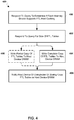
- the various aspects of the FTL host caching initialization method 300 may include further operations as illustrated in FIG. 4 . Such operations may occur concurrently, in an appropriate order, with the operations illustrated in FIG. 3 .
- the flash memory device 50 may respond to the query from the host device 20 to determine if the flash memory device 50 supports FTL host caching.
- aspects of the FTL host caching initialization method 300 may include the response to this query to be either passive or active. For example, if the response is passive, the host device 20 may read a value in a specific register or memory location of the flash memory device 50 to determine support of FTL host caching.
- the flash memory device 50 may respond to the query from the host device 20 for the size of the FTL tables 68.
- the response may involve returning a value indicating the amount of memory necessary to store a copy of the entirety of the FTL tables.
- the various aspects of this response in block 402 may include active and passive responses. If the host device 20 has granted the flash memory device 50 direct memory access permissions, in block 404 the flash memory device 50 may write the complete copy of the FTL tables 70 to the DRAM 38 of the host device 20.
- the flash memory device 50 may write a partial copy of the FTL tables 70 to the DRAM 38 in block 408 after having been granted flash memory device 50 direct memory access permissions. Once this operation is complete, in block 406 the flash memory device 50 may send a notification to the host device 20 indicating that the copy of the FTL tables 70 are stored in the DRAM 38 of the host device 20.
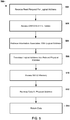
- various aspects of FTL host caching may include the flash memory device 50 reading from and/or writing to the copy of the FTL tables 70 stored in the DRAM 38 of the host device 20.
- a read from the flash memory device 50 operation 500 may be implemented, as illustrated in FIG. 5 .
- the flash memory device 50 may receive a read request, from the host device 20, associated with a logical address of the flash memory 64. Having been informed of the requested operation and logical address, the flash memory device 50 may initiate the write operation.
- the flash memory device 50 may directly access the copy of the FTL tables 70 located in the DRAM 38 of the host device 20.
- the permissions granted to the flash memory device 50 for direct memory access to the DRAM 38 may allow the flash memory device 50 to bus master, or issue commands over, the storage bus 40 connecting the devices 20, 50.
- the flash memory device 50 may read/retrieve information from the copy of the FTL tables 70 associated with the logical address.
- FIG. 6 illustrates a write to the flash memory device 50 operation 600 may be implemented.
- the flash memory device 50 may receive a write request, from the host device 20, associated with a logical address of the flash memory 64. Informed of the requested operation and logical address, the flash memory device 50 may initiate the write operation.
- the flash memory device 50 may now directly access the copy of the FTL tables 70 located in the DRAM 38 of the host device 20.
- the permissions granted to the flash memory device 50 for direct memory access to the DRAM 38 may allow the flash memory device 50 to bus master, or issue commands over, the storage bus 40 connecting the devices 20, 50.
- the flash memory device 50 may read/retrieve information from the copy of the FTL tables 70 associated with the logical address.
- the flash storage device 50 may retrieve from the tables in the SRAM 58 free storage space and/or wear leveling information relating to the flash memory 64 for space suitable for storing the data. With this information, in block 624 the flash storage device 50 may determine the physical address of where to write the data to the memory, access the flash memory 64 in block 610, and continue with the remainder of the write to the flash memory device 50 operation 600 as described herein.
- aspects may include updating the FTL tables 68 to reflect the changes that have been made to the copy of the FTL tables 70.
- One such aspect may include updating the FTL tables 68 as part of or after the write to the flash memory device 50 operation 600.
- the FTL tables 68 may be updated at any point after updating the copy of the FTL tables 70.
- Such an update may include copying the copy of the FTL tables 70 or copying just the updates to the copy of the FTL tables 70 to the flash memory 64. It is also conceived that the updates to the FTL tables 68 may occur before or concurrently with the updates to the copy of the FTL tables.
- Further aspects may include updating the FTL tables 68 by a predefined rule or dynamically based on available resources.
- the predefined rule may execute an update of the FTL tables 68 periodically, based on a schedule, available resources, in response to a command, or based on a set of parameters. Updating the FTL tables 68 dynamically, for example, may occur based on a determination by either or both devices 20, 50, of the available resources, power, and/or time needed to execute the update with the lowest cost on the performance of the FTL host caching system 10. Such times may be when the FTL host caching system 10 is idle or minimal processes are running.
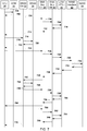
- FIG. 7 illustrates an aspect of the process flow of the FTL host caching initialization method 300 during a boot sequence of the host device 20. Aspects are conceived where the FTL host caching initialization method 300 is executed at times other than during a boot sequence of the host device 20. For example, upon a connection of the flash memory device 50 while the host device 20 is running.
- the CPU 24 of the host device 50 sends signal 700 to access boot information in the ROM 30 of the host device 50, such as BIOS and drivers, and to execute code processes of the initialization method 300.
- the CPU 24 may receive the information and the code processes via a return signal 702 from the ROM 30.
- the CPU 24 may check for and initialize connected peripheral devices, like the flash memory device 50, and query for FTL host caching compatibility, and the size of the FTL tables 58. To do so, the CPU 24 sends signal 704 to the DMA bus controller 26 of the host device 50, which may be forwarded as signal 706 to the DMA bus controller 54 of the flash memory device 50. The signal 706 may be forwarded to the microcontroller 56 of the flash memory device 50 as signal 708. In some aspects the microcontroller 56 may respond to the query of the CPU 24 by sending a response signal 710 back to the CPU 24 via the DMA bus controller 54, forwarding signal 710 as signal 712 to the DMA bus controller and as signal 714 to the CPU 24.
- the CPU 24 may provide the microcontroller 56 direct memory access to the DRAM 38 and request the copy of the FTL tables 70 by sending a signal 724 to DMA bus controller 26.
- Signal 724 may be forwarded to the DMA bus controller 54 as signal 726 and to the microcontroller 56 as signal 728.
- the microcontroller 56 may send signal 730 to access the FTL tables 58 in the flash memory 64 and retrieve the copy of the FTL tables 70.
- the memory interface 60 receives signal 730 and interprets it as signal 732, which is sent to the flash memory 64.
- the memory interface 60 receives a return signal 734 from the memory 64 representing the copy of the FTL tables 70, and forwards signal 734 as signal 736 to the microcontroller 56.
- the microcontroller 56 may signal to the CPU 24 that the FTL host caching initialization method 300 is complete by sending signal 754.
- the DMA bus controller 54 may receive signal 754 and forward it as signal 756 to the DMA bus controller 16, which may forward signal 758 to the CPU 24.
- the CPU 24 may acknowledge the completion of the FTL host cashing initialization method 300 and instruct or give permission to the microcontroller to begin using the copy of the FTL tables 70 in the DRAM 38 for read and write operations by sending signal 760.
- the DMA bus controller 26 may receive the signal 760 and forward it to the DMA bus controller 54 as signal 762, which may be relayed from the DMA bus controller 54 to the microcontroller 56 as signal 764.
- the microcontroller 56 may return an acknowledgement of the permission from the CPU 24 as signal 766.
- the DMA bus controller 54 may receive the signal 766 and forward it to the DMA bus controller 26 as signal 768, and to the CPU 24 as signal 780 from the DMA bus controller 26.
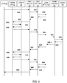
- the CPU 24 may issue the read request for the logical address to the microcontroller 56, sending the signal 800 carrying the request through the DMA bus controller 26 as signal 802.
- the DMA controller 54 may receive signal 802 and forward it to the microcontroller 56 as signal 804.
- the microcontroller 56 may access the memory 64 and retrieve/read data located at the physical address by sending signal 822.
- the memory interface 60 may interpret the signal 822 and send signal 824 to the memory 64.
- a return signal 826 from the memory 64 representing the information at the physical address may be received by the memory interface 60 and sent to the microcontroller 56 as signal 828.
- the microcontroller 56 may forward the retrieved data to the DRAM 38 for use by the CPU 24 by sending signal 830.
- the DMA bus controller 54 may receive signal 830 and forward it to the DMA bus controller 26 as signal 832, which may be forwarded to the DRAM controller 32 as signal 834.
- the microcontroller 56 may send a notification to the CPU 24 that the requested read operation is complete and the data is available in the DRAM 38 by sending signal 846.
- the DMA bus controller 54 may receive the notification signal 846 and forward it to the DMA bus controller 26 as signal 848, which may be forwarded to the CPU 24 as signal 850.
- FIG. 9 illustrates an aspect of the process flow of the write to the flash memory device 50 operation 600.
- the CPU 24 may issue the write request for the logical address to the microcontroller 56, sending a signal 900 carrying the request through the DMA bus controller 26 as signal 902.
- the DMA controller 54 may receive signal 902 and forward it to the microcontroller 56 as signal 904.
- the DRAM controller 32 may receive a return signal 914 from the DRAM 38, which may be sent to the DMA bus controller 26 as signal 916, forwarded to DMA bus controller 54 as signal 918, and finally received by the microcontroller 56 as signal 920. With the information retrieved from the copy of the FTL tables 70, the microcontroller 56 may now translate the logical address to the physical address of the flash memory 64.
- the microcontroller 56 may retrieve the write data from the DRAM 38 by sending signal 922.
- the DMA bus controller 54 may receive signal 922 and forward it as signal 924 to the DMA bus controller 26.
- the DRAM controller 32 may receive the signal 926 from the DMA bus controller 26 and interpret it as signal 928 and send the signal 928 to the DRAM 38.
- the DRAM controller 32 may receive the write data read from the DRAM 38 as signal 930 and forward the write data to the microcontroller 56 as signal 932.
- the DMA bus controller 26 may receive the signal 932 and forward it as signal 934 to the DMA bus controller 54, which may be forwarded to the microcontroller 56 as signal 936.
- the microcontroller 56 may access and write data to memory 64 at the physical address by sending signal 938.
- the memory interface 60 may interpret the signal 938 and send signal 940 to the memory 64.
- the memory interface 60 may identify when the writing to the memory 64 is complete by receiving a return signal 942 from the memory 64, and send signal 944 to the microcontroller 56 to indicate the writing is complete.
- the microcontroller 56 may update the copy of the FTL tables 70 by bus mastering the busses 34, 40, connecting it to the DRAM 38.
- the microcontroller may send signal 946 to write directly to the DRAM 38.
- the DMA bus controller 54 may forward signal 946 to the DMA bus controller 26 as signal 948, which may be forwarded to the DRAM controller 32 as signal 950.
- the DRAM controller 32 may interpret signal 950 and send signal 952 to the DRAM 38.
- the DRAM controller 32 may identify when the update of the copy of the FTL tables 70 is complete by receiving a return signal 954 from the DRAM 38.
- the signal 954 may be sent to the DMA bus controller 26 as signal 956, forwarded to DMA bus controller 54 as signal 958, and finally received by the microcontroller 56 as signal 960.
- FIG. 10 illustrates an aspect of the process flow of the write to the flash memory device 50 operation 600.
- the CPU 24 may issue the write request for to the microcontroller 56, sending a signal 1000 carrying the request through the DMA bus controller 26 as signal 1002.
- the DMA controller 54 may receive signal 1002 and forward it to the microcontroller 56 as signal 1004.
- the microcontroller 56 may access the memory 64 write data to memory 64 at the physical address by sending signal 1026.
- the memory interface 60 may interpret the signal 1026 and send signal 1028 to the memory 64.
- the memory interface 60 may identify when the writing to the memory 64 is complete by receiving a return signal 1030 from the memory 64, and send signal 1032 to the microcontroller 56 to indicate the writing is complete.
- the microcontroller 56 may update the copy of the FTL tables 70 by bus mastering the busses 34, 40, connecting it to the DRAM 38.
- the microcontroller may send signal 1034 to write directly to the DRAM 38.
- the DMA bus controller 54 may forward signal 1034 to the DMA bus controller 26 as signal 1036, which may be forwarded to the DRAM controller 32 as signal 1038.
- the DRAM controller 32 may interpret signal 1038 and send signal 1040 to the DRAM 38.
- the DRAM controller 32 may identify when the update of the copy of the FTL tables 70 is complete by receiving a return signal 1042 from the DRAM 38.
- the signal 1042 may be sent to the DMA bus controller 26 as signal 1044, forwarded to DMA bus controller 54 as signal 1046, and finally received by the microcontroller 56 as signal 1048.
- the microcontroller 56 may notify the CPU 24 that the operation 600 is complete by sending signal 1050.
- the DMA bus controllers 54 may receive signal 1050 and forward it to the DMA bus controller 26 as signal 1052, which may be forwarded to the CPU 24 as signal 1054.
- any portion of the process flow between any of the components may be repeated more than shown in FIGs. 7-10 for one of more of the processes described herein.
- signals 734-758 representing copying the FTL tables 68 from the flash memory device 50 to the host device, may occur numerous times as transactions of the copying. The transactions may be executions of the copying where each transaction copies a portion of the FTL tables 68, and the transactions continue until the copying is complete. Taking an example of 32MB of FTL table data, only 32, 64, or 128 bytes of FTL table data may be copied to the host device 20 per transaction. The same holds true for any read or write operation depicted in FIGs. 7-10 .
- a processor may also be implemented as a combination of computing devices, e.g., a combination of a DSP and a microprocessor, a plurality of microprocessors, one or more microprocessors in conjunction with a DSP core, or any other such configuration. Alternatively, some operations or methods may be performed by circuitry that is specific to a given function.
Applications Claiming Priority (2)
| Application Number | Priority Date | Filing Date | Title |
|---|---|---|---|
| US13/892,433 US9575884B2 (en) | 2013-05-13 | 2013-05-13 | System and method for high performance and low cost flash translation layer |
| PCT/US2014/037531 WO2014186232A1 (en) | 2013-05-13 | 2014-05-09 | System and method for high performance and low cost flash translation layer |
Publications (2)
| Publication Number | Publication Date |
|---|---|
| EP2997459A1 EP2997459A1 (en) | 2016-03-23 |
| EP2997459B1 true EP2997459B1 (en) | 2018-03-07 |
Family
ID=50942864
Family Applications (1)
| Application Number | Title | Priority Date | Filing Date |
|---|---|---|---|
| EP14730327.5A Not-in-force EP2997459B1 (en) | 2013-05-13 | 2014-05-09 | System and method for high performance and low cost flash translation layer |
Country Status (8)
| Country | Link |
|---|---|
| US (1) | US9575884B2 (ja) |
| EP (1) | EP2997459B1 (ja) |
| JP (1) | JP6190045B2 (ja) |
| KR (1) | KR20160006709A (ja) |
| CN (1) | CN105378642A (ja) |
| BR (1) | BR112015028634A2 (ja) |
| TW (1) | TWI556099B (ja) |
| WO (1) | WO2014186232A1 (ja) |
Families Citing this family (57)
| Publication number | Priority date | Publication date | Assignee | Title |
|---|---|---|---|---|
| KR20150139718A (ko) * | 2014-06-03 | 2015-12-14 | 에스케이하이닉스 주식회사 | 불휘발성 메모리를 제어하는 컨트롤러 및 그것을 포함하는 반도체 장치 |
| US9507722B2 (en) * | 2014-06-05 | 2016-11-29 | Sandisk Technologies Llc | Methods, systems, and computer readable media for solid state drive caching across a host bus |
| US9563382B2 (en) | 2014-06-05 | 2017-02-07 | Sandisk Technologies Llc | Methods, systems, and computer readable media for providing flexible host memory buffer |
| US10007442B2 (en) | 2014-08-20 | 2018-06-26 | Sandisk Technologies Llc | Methods, systems, and computer readable media for automatically deriving hints from accesses to a storage device and from file system metadata and for optimizing utilization of the storage device based on the hints |
| US10268584B2 (en) * | 2014-08-20 | 2019-04-23 | Sandisk Technologies Llc | Adaptive host memory buffer (HMB) caching using unassisted hinting |
| US10228854B2 (en) | 2014-08-20 | 2019-03-12 | Sandisk Technologies Llc | Storage devices and methods for optimizing use of storage devices based on storage device parsing of file system metadata in host write operations |
| US9851901B2 (en) | 2014-09-26 | 2017-12-26 | Western Digital Technologies, Inc. | Transfer of object memory references in a data storage device |
| US10007433B2 (en) * | 2015-01-21 | 2018-06-26 | Sandisk Technologies Llc | Systems and methods for performing adaptive host memory buffer caching of transition layer tables |
| US10101918B2 (en) | 2015-01-21 | 2018-10-16 | Sandisk Technologies Llc | Systems and methods for generating hint information associated with a host command |
| KR20160120004A (ko) * | 2015-04-07 | 2016-10-17 | 삼성전자주식회사 | 시스템 온-칩 및 이를 포함하는 전자 기기 |
| CN106155579A (zh) * | 2015-04-27 | 2016-11-23 | 广明光电股份有限公司 | 固态硬盘动态储存转换层数据的方法 |
| CN106293493A (zh) * | 2015-05-18 | 2017-01-04 | 广明光电股份有限公司 | 固态硬盘模块动态储存转换层的方法 |
| US10055236B2 (en) * | 2015-07-02 | 2018-08-21 | Sandisk Technologies Llc | Runtime data storage and/or retrieval |
| US10452556B2 (en) | 2015-09-11 | 2019-10-22 | Toshiba Memory Corporation | Memory device and information processing device |
| TWI553478B (zh) * | 2015-09-23 | 2016-10-11 | 瑞昱半導體股份有限公司 | 能夠使用外部揮發性記憶體的裝置以及能夠釋放內部揮發性記憶體的裝置 |
| CN106557271B (zh) * | 2015-09-30 | 2019-08-20 | 合肥沛睿微电子股份有限公司 | 能够使用外部挥发性记忆体的装置以及能够释放内部挥发性记忆体的装置 |
| US10452594B2 (en) | 2015-10-20 | 2019-10-22 | Texas Instruments Incorporated | Nonvolatile logic memory for computing module reconfiguration |
| TWI556100B (zh) * | 2015-10-26 | 2016-11-01 | 點序科技股份有限公司 | 快閃記憶體裝置及其交錯存取方法 |
| CN105353989B (zh) | 2015-11-19 | 2018-12-28 | 华为技术有限公司 | 存储数据访问方法及相关的控制器、设备、主机和系统 |
| US20170177497A1 (en) * | 2015-12-21 | 2017-06-22 | Qualcomm Incorporated | Compressed caching of a logical-to-physical address table for nand-type flash memory |
| US9927997B2 (en) | 2015-12-21 | 2018-03-27 | Sandisk Technologies Llc | Methods, systems, and computer readable media for automatically and selectively enabling burst mode operation in a storage device |
| US10331203B2 (en) | 2015-12-29 | 2019-06-25 | Texas Instruments Incorporated | Compute through power loss hardware approach for processing device having nonvolatile logic memory |
| US10114743B2 (en) * | 2016-04-06 | 2018-10-30 | Sandisk Technologies Inc. | Memory erase management |
| US10157004B2 (en) | 2016-04-14 | 2018-12-18 | Sandisk Technologies Llc | Storage system and method for recovering data corrupted in a host memory buffer |
| US10474374B2 (en) * | 2016-05-24 | 2019-11-12 | Samsung Electronics Co., Ltd. | Method and apparatus for storage device latency/bandwidth self monitoring |
| CN109074318B (zh) * | 2016-05-31 | 2023-07-04 | 桑迪士克科技有限责任公司 | 用于执行转换层表的自适应主机存储器缓冲区高速缓存的系统和方法 |
| US10521118B2 (en) | 2016-07-13 | 2019-12-31 | Sandisk Technologies Llc | Methods, systems, and computer readable media for write classification and aggregation using host memory buffer (HMB) |
| US10503635B2 (en) * | 2016-09-22 | 2019-12-10 | Dell Products, Lp | System and method for adaptive optimization for performance in solid state drives based on segment access frequency |
| CN107870870B (zh) * | 2016-09-28 | 2021-12-14 | 北京忆芯科技有限公司 | 访问超过地址总线宽度的内存空间 |
| CN107870867B (zh) * | 2016-09-28 | 2021-12-14 | 北京忆芯科技有限公司 | 32位cpu访问大于4gb内存空间的方法与装置 |
| US10853233B2 (en) * | 2016-10-18 | 2020-12-01 | Toshiba Memory Corporation | Reconstruction of address mapping in a host of a storage system |
| CN108121664A (zh) * | 2016-11-28 | 2018-06-05 | 慧荣科技股份有限公司 | 数据储存装置以及其操作方法 |
| TWI691839B (zh) * | 2016-11-28 | 2020-04-21 | 慧榮科技股份有限公司 | 資料管理方法 |
| US11256431B1 (en) | 2017-01-13 | 2022-02-22 | Lightbits Labs Ltd. | Storage system having a field programmable gate array |
| KR20180121733A (ko) * | 2017-04-28 | 2018-11-08 | 에스케이하이닉스 주식회사 | 데이터 저장 장치 및 그것의 동작 방법 |
| US10558393B2 (en) * | 2017-10-20 | 2020-02-11 | Qualcomm Incorporated | Controller hardware automation for host-aware performance booster |
| JP2019079464A (ja) * | 2017-10-27 | 2019-05-23 | 東芝メモリ株式会社 | メモリシステムおよび制御方法 |
| US10409726B2 (en) | 2017-10-30 | 2019-09-10 | Micron Technology, Inc. | Dynamic L2P cache |
| KR102384759B1 (ko) * | 2017-11-13 | 2022-04-11 | 삼성전자주식회사 | 호스트 메모리 버퍼를 사용하기 위해 호스트 장치와 속성 정보를 공유하는 스토리지 장치 및 그것을 포함하는 전자 장치 |
| US11294440B2 (en) | 2017-11-17 | 2022-04-05 | Hewlett-Packard Development Company, L.P. | Peripheral device configurations by host systems |
| US10459844B2 (en) * | 2017-12-21 | 2019-10-29 | Western Digital Technologies, Inc. | Managing flash memory read operations |
| US10725983B2 (en) * | 2017-12-29 | 2020-07-28 | Huawei Technologies Co., Ltd. | Systems and methods for database management using append-only storage devices |
| TWI679538B (zh) | 2018-03-31 | 2019-12-11 | 慧榮科技股份有限公司 | 資料儲存系統之控制單元以及邏輯至物理映射表更新方法 |
| CN112166420B (zh) * | 2018-04-23 | 2024-04-05 | 美光科技公司 | 用于刷新逻辑到物理信息的系统和方法 |
| US10884920B2 (en) | 2018-08-14 | 2021-01-05 | Western Digital Technologies, Inc. | Metadata-based operations for use with solid state devices |
| US11340810B2 (en) | 2018-10-09 | 2022-05-24 | Western Digital Technologies, Inc. | Optimizing data storage device operation by grouping logical block addresses and/or physical block addresses using hints |
| US11249664B2 (en) * | 2018-10-09 | 2022-02-15 | Western Digital Technologies, Inc. | File system metadata decoding for optimizing flash translation layer operations |
| KR20200046264A (ko) | 2018-10-24 | 2020-05-07 | 삼성전자주식회사 | 호스트 메모리 버퍼를 이용하는 데이터 스토리지 장치 및 그 동작 방법 |
| KR102599176B1 (ko) | 2018-11-14 | 2023-11-08 | 삼성전자주식회사 | 호스트 메모리 버퍼를 사용하는 스토리지 장치 및 그것의 메모리 관리 방법 |
| CN111367830B (zh) * | 2018-12-06 | 2023-11-14 | 北京忆恒创源科技股份有限公司 | 主机参与的重建ftl表的方法及其存储设备 |
| KR20200069889A (ko) * | 2018-12-07 | 2020-06-17 | 에스케이하이닉스 주식회사 | 컨트롤러, 이를 포함하는 메모리 시스템 및 이의 동작 방법 |
| KR20200088635A (ko) * | 2019-01-15 | 2020-07-23 | 에스케이하이닉스 주식회사 | 메모리 시스템 및 메모리 시스템의 동작방법 |
| JP2022522437A (ja) * | 2019-04-30 | 2022-04-19 | 長江存儲科技有限責任公司 | コントローラ、機器および方法 |
| KR20200143871A (ko) | 2019-06-17 | 2020-12-28 | 삼성전자주식회사 | 스토리지를 포함하는 전자 장치 및 그의 스토리지 이용 방법 |
| KR20210068699A (ko) | 2019-12-02 | 2021-06-10 | 삼성전자주식회사 | 스토리지 장치, 스토리지 시스템 및 스토리지 장치의 동작 방법 |
| CN111177033A (zh) * | 2019-12-24 | 2020-05-19 | 河南文正电子数据处理有限公司 | 一种固态硬盘的使用方法 |
| KR20220080254A (ko) * | 2020-12-07 | 2022-06-14 | 에스케이하이닉스 주식회사 | 메모리 시스템 및 메모리 시스템의 컨트롤러 |
Family Cites Families (26)
| Publication number | Priority date | Publication date | Assignee | Title |
|---|---|---|---|---|
| US6014724A (en) * | 1995-10-27 | 2000-01-11 | Scm Microsystems (U.S.) Inc. | Flash translation layer block indication map revision system and method |
| US6484218B1 (en) * | 1998-10-08 | 2002-11-19 | Texas Instruments Incorporated | Method for improving direct memory access performance |
| JP2001243110A (ja) * | 1999-12-20 | 2001-09-07 | Tdk Corp | メモリコントローラ、フラッシュメモリシステム及びフラッシュメモリへのアクセス方法 |
| JP4199519B2 (ja) * | 2002-11-05 | 2008-12-17 | パナソニック株式会社 | メモリ管理装置及びメモリ管理方法 |
| US8041878B2 (en) | 2003-03-19 | 2011-10-18 | Samsung Electronics Co., Ltd. | Flash file system |
| US6981123B2 (en) * | 2003-05-22 | 2005-12-27 | Seagate Technology Llc | Device-managed host buffer |
| US20050138464A1 (en) * | 2003-11-21 | 2005-06-23 | Chong Pohsoon | Scratch fill using scratch tracking table |
| TW200832440A (en) | 2007-01-25 | 2008-08-01 | Genesys Logic Inc | Flash memory translation layer system |
| KR101663667B1 (ko) | 2009-02-03 | 2016-10-07 | 삼성전자주식회사 | 플래시 메모리의 주소 매핑에 의한 데이터 관리 방법 및 장치 |
| US8219776B2 (en) | 2009-09-23 | 2012-07-10 | Lsi Corporation | Logical-to-physical address translation for solid state disks |
| US8874824B2 (en) * | 2009-06-04 | 2014-10-28 | Memory Technologies, LLC | Apparatus and method to share host system RAM with mass storage memory RAM |
| EP2264602A1 (en) | 2009-06-17 | 2010-12-22 | Gemalto SA | Memory device for managing the recovery of a non volatile memory |
| CN102201259A (zh) * | 2010-03-24 | 2011-09-28 | 建兴电子科技股份有限公司 | 非易失性存储器的平均抹写方法 |
| KR20110121897A (ko) | 2010-05-03 | 2011-11-09 | 삼성전자주식회사 | 사용자 장치 및 그것의 프로그램 페일 처리 방법 |
| US8966176B2 (en) * | 2010-05-27 | 2015-02-24 | Sandisk Il Ltd. | Memory management storage to a host device |
| KR20120081351A (ko) * | 2011-01-11 | 2012-07-19 | 에스케이하이닉스 주식회사 | Ftl을 수행하는 비휘발성 메모리 장치 및 그의 제어 방법 |
| JP5405513B2 (ja) * | 2011-03-22 | 2014-02-05 | 株式会社東芝 | メモリシステム、不揮発性記憶装置、不揮発性記憶装置の制御方法、及びプログラム |
| JP2012243287A (ja) * | 2011-05-24 | 2012-12-10 | Sony Corp | 情報処理装置および情報処理方法 |
| US8806112B2 (en) | 2011-07-14 | 2014-08-12 | Lsi Corporation | Meta data handling within a flash media controller |
| KR101856506B1 (ko) | 2011-09-22 | 2018-05-11 | 삼성전자주식회사 | 데이터 저장 장치 및 그것의 데이터 쓰기 방법 |
| CN102541760B (zh) * | 2012-01-04 | 2015-05-20 | 记忆科技(深圳)有限公司 | 基于固态硬盘的计算机系统 |
| US9213632B1 (en) * | 2012-02-29 | 2015-12-15 | Marvell International Ltd. | Systems and methods for data storage devices to use external resources |
| US9116820B2 (en) * | 2012-08-28 | 2015-08-25 | Memory Technologies Llc | Dynamic central cache memory |
| KR102015906B1 (ko) * | 2012-11-12 | 2019-08-29 | 삼성전자주식회사 | 불휘발성 메모리 장치를 포함하는 메모리 시스템 및 그것의 읽기 방법 |
| US9329991B2 (en) * | 2013-01-22 | 2016-05-03 | Seagate Technology Llc | Translation layer partitioned between host and controller |
| US9122588B1 (en) * | 2013-03-15 | 2015-09-01 | Virident Systems Inc. | Managing asymmetric memory system as a cache device |
-
2013
- 2013-05-13 US US13/892,433 patent/US9575884B2/en active Active
-
2014
- 2014-05-09 WO PCT/US2014/037531 patent/WO2014186232A1/en active Application Filing
- 2014-05-09 JP JP2016513995A patent/JP6190045B2/ja active Active
- 2014-05-09 EP EP14730327.5A patent/EP2997459B1/en not_active Not-in-force
- 2014-05-09 BR BR112015028634A patent/BR112015028634A2/pt not_active Application Discontinuation
- 2014-05-09 KR KR1020157033238A patent/KR20160006709A/ko active IP Right Grant
- 2014-05-09 CN CN201480026743.4A patent/CN105378642A/zh active Pending
- 2014-05-13 TW TW103116876A patent/TWI556099B/zh not_active IP Right Cessation
Also Published As
| Publication number | Publication date |
|---|---|
| WO2014186232A1 (en) | 2014-11-20 |
| KR20160006709A (ko) | 2016-01-19 |
| TW201506619A (zh) | 2015-02-16 |
| US20140337560A1 (en) | 2014-11-13 |
| JP2016522942A (ja) | 2016-08-04 |
| TWI556099B (zh) | 2016-11-01 |
| BR112015028634A2 (pt) | 2017-07-25 |
| JP6190045B2 (ja) | 2017-08-30 |
| CN105378642A (zh) | 2016-03-02 |
| US9575884B2 (en) | 2017-02-21 |
| EP2997459A1 (en) | 2016-03-23 |
Similar Documents
| Publication | Publication Date | Title |
|---|---|---|
| EP2997459B1 (en) | System and method for high performance and low cost flash translation layer | |
| KR101779723B1 (ko) | 영구 저장소로의 라이트백을 요구하는 비 트랜잭션 코드 영역의 시작과 끝을 마킹하는 명령어들 | |
| US9817652B2 (en) | Data storage device and method for reducing firmware update time and data processing system including the device | |
| US9535827B2 (en) | RAM disk using non-volatile random access memory | |
| US11341059B2 (en) | Using multiple memory elements in an input-output memory management unit for performing virtual address to physical address translations | |
| KR102156222B1 (ko) | 데이터 저장 장치 및 그것을 포함하는 데이터 처리 시스템 | |
| US20170255561A1 (en) | Technologies for increasing associativity of a direct-mapped cache using compression | |
| KR102285275B1 (ko) | 하이브리드 메모리 드라이브, 컴퓨터 시스템, 및 멀티 모드 하이브리드 드라이브를 동작시키기 위한 관련 방법 | |
| EP3183659B1 (en) | Power aware padding | |
| KR20160025292A (ko) | 데이터 저장 장치, 그것을 포함하는 데이터 처리 시스템 및 그것의 동작 방법 | |
| CN110597742A (zh) | 用于具有持久系统存储器的计算机系统的改进存储模型 | |
| US11775188B2 (en) | Communications to reclaim storage space occupied by proof of space plots in solid state drives | |
| US20170153994A1 (en) | Mass storage region with ram-disk access and dma access | |
| US11386012B1 (en) | Increasing address space layout randomization entropy via page remapping and rotations | |
| US20230305743A1 (en) | Memory controller and memory system including the same |
Legal Events
| Date | Code | Title | Description |
|---|---|---|---|
| PUAI | Public reference made under article 153(3) epc to a published international application that has entered the european phase |
Free format text: ORIGINAL CODE: 0009012 |
|
| 17P | Request for examination filed |
Effective date: 20151106 |
|
| AK | Designated contracting states |
Kind code of ref document: A1 Designated state(s): AL AT BE BG CH CY CZ DE DK EE ES FI FR GB GR HR HU IE IS IT LI LT LU LV MC MK MT NL NO PL PT RO RS SE SI SK SM TR |
|
| AX | Request for extension of the european patent |
Extension state: BA ME |
|
| DAX | Request for extension of the european patent (deleted) | ||
| 17Q | First examination report despatched |
Effective date: 20161223 |
|
| GRAP | Despatch of communication of intention to grant a patent |
Free format text: ORIGINAL CODE: EPIDOSNIGR1 |
|
| INTG | Intention to grant announced |
Effective date: 20170925 |
|
| GRAS | Grant fee paid |
Free format text: ORIGINAL CODE: EPIDOSNIGR3 |
|
| GRAA | (expected) grant |
Free format text: ORIGINAL CODE: 0009210 |
|
| AK | Designated contracting states |
Kind code of ref document: B1 Designated state(s): AL AT BE BG CH CY CZ DE DK EE ES FI FR GB GR HR HU IE IS IT LI LT LU LV MC MK MT NL NO PL PT RO RS SE SI SK SM TR |
|
| REG | Reference to a national code |
Ref country code: GB Ref legal event code: FG4D |
|
| REG | Reference to a national code |
Ref country code: CH Ref legal event code: EP Ref country code: AT Ref legal event code: REF Ref document number: 977249 Country of ref document: AT Kind code of ref document: T Effective date: 20180315 |
|
| REG | Reference to a national code |
Ref country code: IE Ref legal event code: FG4D |
|
| REG | Reference to a national code |
Ref country code: DE Ref legal event code: R096 Ref document number: 602014022002 Country of ref document: DE |
|
| REG | Reference to a national code |
Ref country code: FR Ref legal event code: PLFP Year of fee payment: 5 |
|
| REG | Reference to a national code |
Ref country code: NL Ref legal event code: MP Effective date: 20180307 |
|
| REG | Reference to a national code |
Ref country code: LT Ref legal event code: MG4D |
|
| PG25 | Lapsed in a contracting state [announced via postgrant information from national office to epo] |
Ref country code: NO Free format text: LAPSE BECAUSE OF FAILURE TO SUBMIT A TRANSLATION OF THE DESCRIPTION OR TO PAY THE FEE WITHIN THE PRESCRIBED TIME-LIMIT Effective date: 20180607 Ref country code: CY Free format text: LAPSE BECAUSE OF FAILURE TO SUBMIT A TRANSLATION OF THE DESCRIPTION OR TO PAY THE FEE WITHIN THE PRESCRIBED TIME-LIMIT Effective date: 20180307 Ref country code: LT Free format text: LAPSE BECAUSE OF FAILURE TO SUBMIT A TRANSLATION OF THE DESCRIPTION OR TO PAY THE FEE WITHIN THE PRESCRIBED TIME-LIMIT Effective date: 20180307 Ref country code: FI Free format text: LAPSE BECAUSE OF FAILURE TO SUBMIT A TRANSLATION OF THE DESCRIPTION OR TO PAY THE FEE WITHIN THE PRESCRIBED TIME-LIMIT Effective date: 20180307 Ref country code: ES Free format text: LAPSE BECAUSE OF FAILURE TO SUBMIT A TRANSLATION OF THE DESCRIPTION OR TO PAY THE FEE WITHIN THE PRESCRIBED TIME-LIMIT Effective date: 20180307 Ref country code: HR Free format text: LAPSE BECAUSE OF FAILURE TO SUBMIT A TRANSLATION OF THE DESCRIPTION OR TO PAY THE FEE WITHIN THE PRESCRIBED TIME-LIMIT Effective date: 20180307 |
|
| REG | Reference to a national code |
Ref country code: AT Ref legal event code: MK05 Ref document number: 977249 Country of ref document: AT Kind code of ref document: T Effective date: 20180307 |
|
| PG25 | Lapsed in a contracting state [announced via postgrant information from national office to epo] |
Ref country code: RS Free format text: LAPSE BECAUSE OF FAILURE TO SUBMIT A TRANSLATION OF THE DESCRIPTION OR TO PAY THE FEE WITHIN THE PRESCRIBED TIME-LIMIT Effective date: 20180307 Ref country code: SE Free format text: LAPSE BECAUSE OF FAILURE TO SUBMIT A TRANSLATION OF THE DESCRIPTION OR TO PAY THE FEE WITHIN THE PRESCRIBED TIME-LIMIT Effective date: 20180307 Ref country code: BG Free format text: LAPSE BECAUSE OF FAILURE TO SUBMIT A TRANSLATION OF THE DESCRIPTION OR TO PAY THE FEE WITHIN THE PRESCRIBED TIME-LIMIT Effective date: 20180607 Ref country code: LV Free format text: LAPSE BECAUSE OF FAILURE TO SUBMIT A TRANSLATION OF THE DESCRIPTION OR TO PAY THE FEE WITHIN THE PRESCRIBED TIME-LIMIT Effective date: 20180307 Ref country code: GR Free format text: LAPSE BECAUSE OF FAILURE TO SUBMIT A TRANSLATION OF THE DESCRIPTION OR TO PAY THE FEE WITHIN THE PRESCRIBED TIME-LIMIT Effective date: 20180608 |
|
| PGFP | Annual fee paid to national office [announced via postgrant information from national office to epo] |
Ref country code: FR Payment date: 20180517 Year of fee payment: 5 |
|
| PG25 | Lapsed in a contracting state [announced via postgrant information from national office to epo] |
Ref country code: PL Free format text: LAPSE BECAUSE OF FAILURE TO SUBMIT A TRANSLATION OF THE DESCRIPTION OR TO PAY THE FEE WITHIN THE PRESCRIBED TIME-LIMIT Effective date: 20180307 Ref country code: EE Free format text: LAPSE BECAUSE OF FAILURE TO SUBMIT A TRANSLATION OF THE DESCRIPTION OR TO PAY THE FEE WITHIN THE PRESCRIBED TIME-LIMIT Effective date: 20180307 Ref country code: RO Free format text: LAPSE BECAUSE OF FAILURE TO SUBMIT A TRANSLATION OF THE DESCRIPTION OR TO PAY THE FEE WITHIN THE PRESCRIBED TIME-LIMIT Effective date: 20180307 Ref country code: NL Free format text: LAPSE BECAUSE OF FAILURE TO SUBMIT A TRANSLATION OF THE DESCRIPTION OR TO PAY THE FEE WITHIN THE PRESCRIBED TIME-LIMIT Effective date: 20180307 Ref country code: IT Free format text: LAPSE BECAUSE OF FAILURE TO SUBMIT A TRANSLATION OF THE DESCRIPTION OR TO PAY THE FEE WITHIN THE PRESCRIBED TIME-LIMIT Effective date: 20180307 Ref country code: AL Free format text: LAPSE BECAUSE OF FAILURE TO SUBMIT A TRANSLATION OF THE DESCRIPTION OR TO PAY THE FEE WITHIN THE PRESCRIBED TIME-LIMIT Effective date: 20180307 |
|
| PG25 | Lapsed in a contracting state [announced via postgrant information from national office to epo] |
Ref country code: SK Free format text: LAPSE BECAUSE OF FAILURE TO SUBMIT A TRANSLATION OF THE DESCRIPTION OR TO PAY THE FEE WITHIN THE PRESCRIBED TIME-LIMIT Effective date: 20180307 Ref country code: SM Free format text: LAPSE BECAUSE OF FAILURE TO SUBMIT A TRANSLATION OF THE DESCRIPTION OR TO PAY THE FEE WITHIN THE PRESCRIBED TIME-LIMIT Effective date: 20180307 Ref country code: AT Free format text: LAPSE BECAUSE OF FAILURE TO SUBMIT A TRANSLATION OF THE DESCRIPTION OR TO PAY THE FEE WITHIN THE PRESCRIBED TIME-LIMIT Effective date: 20180307 Ref country code: CZ Free format text: LAPSE BECAUSE OF FAILURE TO SUBMIT A TRANSLATION OF THE DESCRIPTION OR TO PAY THE FEE WITHIN THE PRESCRIBED TIME-LIMIT Effective date: 20180307 |
|
| REG | Reference to a national code |
Ref country code: DE Ref legal event code: R097 Ref document number: 602014022002 Country of ref document: DE |
|
| REG | Reference to a national code |
Ref country code: CH Ref legal event code: PL |
|
| PG25 | Lapsed in a contracting state [announced via postgrant information from national office to epo] |
Ref country code: PT Free format text: LAPSE BECAUSE OF FAILURE TO SUBMIT A TRANSLATION OF THE DESCRIPTION OR TO PAY THE FEE WITHIN THE PRESCRIBED TIME-LIMIT Effective date: 20180709 |
|
| PLBE | No opposition filed within time limit |
Free format text: ORIGINAL CODE: 0009261 |
|
| STAA | Information on the status of an ep patent application or granted ep patent |
Free format text: STATUS: NO OPPOSITION FILED WITHIN TIME LIMIT |
|
| REG | Reference to a national code |
Ref country code: BE Ref legal event code: MM Effective date: 20180531 |
|
| PG25 | Lapsed in a contracting state [announced via postgrant information from national office to epo] |
Ref country code: MC Free format text: LAPSE BECAUSE OF FAILURE TO SUBMIT A TRANSLATION OF THE DESCRIPTION OR TO PAY THE FEE WITHIN THE PRESCRIBED TIME-LIMIT Effective date: 20180307 Ref country code: DK Free format text: LAPSE BECAUSE OF FAILURE TO SUBMIT A TRANSLATION OF THE DESCRIPTION OR TO PAY THE FEE WITHIN THE PRESCRIBED TIME-LIMIT Effective date: 20180307 |
|
| 26N | No opposition filed |
Effective date: 20181210 |
|
| REG | Reference to a national code |
Ref country code: IE Ref legal event code: MM4A |
|
| PG25 | Lapsed in a contracting state [announced via postgrant information from national office to epo] |
Ref country code: SI Free format text: LAPSE BECAUSE OF FAILURE TO SUBMIT A TRANSLATION OF THE DESCRIPTION OR TO PAY THE FEE WITHIN THE PRESCRIBED TIME-LIMIT Effective date: 20180307 Ref country code: CH Free format text: LAPSE BECAUSE OF NON-PAYMENT OF DUE FEES Effective date: 20180531 Ref country code: LI Free format text: LAPSE BECAUSE OF NON-PAYMENT OF DUE FEES Effective date: 20180531 |
|
| PG25 | Lapsed in a contracting state [announced via postgrant information from national office to epo] |
Ref country code: LU Free format text: LAPSE BECAUSE OF NON-PAYMENT OF DUE FEES Effective date: 20180509 |
|
| PG25 | Lapsed in a contracting state [announced via postgrant information from national office to epo] |
Ref country code: IE Free format text: LAPSE BECAUSE OF NON-PAYMENT OF DUE FEES Effective date: 20180509 |
|
| PG25 | Lapsed in a contracting state [announced via postgrant information from national office to epo] |
Ref country code: BE Free format text: LAPSE BECAUSE OF NON-PAYMENT OF DUE FEES Effective date: 20180531 |
|
| PG25 | Lapsed in a contracting state [announced via postgrant information from national office to epo] |
Ref country code: MT Free format text: LAPSE BECAUSE OF NON-PAYMENT OF DUE FEES Effective date: 20180509 |
|
| PG25 | Lapsed in a contracting state [announced via postgrant information from national office to epo] |
Ref country code: TR Free format text: LAPSE BECAUSE OF FAILURE TO SUBMIT A TRANSLATION OF THE DESCRIPTION OR TO PAY THE FEE WITHIN THE PRESCRIBED TIME-LIMIT Effective date: 20180307 |
|
| PG25 | Lapsed in a contracting state [announced via postgrant information from national office to epo] |
Ref country code: HU Free format text: LAPSE BECAUSE OF FAILURE TO SUBMIT A TRANSLATION OF THE DESCRIPTION OR TO PAY THE FEE WITHIN THE PRESCRIBED TIME-LIMIT; INVALID AB INITIO Effective date: 20140509 Ref country code: FR Free format text: LAPSE BECAUSE OF NON-PAYMENT OF DUE FEES Effective date: 20190531 Ref country code: MK Free format text: LAPSE BECAUSE OF NON-PAYMENT OF DUE FEES Effective date: 20180307 |
|
| PG25 | Lapsed in a contracting state [announced via postgrant information from national office to epo] |
Ref country code: IS Free format text: LAPSE BECAUSE OF FAILURE TO SUBMIT A TRANSLATION OF THE DESCRIPTION OR TO PAY THE FEE WITHIN THE PRESCRIBED TIME-LIMIT Effective date: 20180707 |
|
| PGFP | Annual fee paid to national office [announced via postgrant information from national office to epo] |
Ref country code: DE Payment date: 20200417 Year of fee payment: 7 |
|
| PGFP | Annual fee paid to national office [announced via postgrant information from national office to epo] |
Ref country code: GB Payment date: 20200429 Year of fee payment: 7 |
|
| REG | Reference to a national code |
Ref country code: DE Ref legal event code: R119 Ref document number: 602014022002 Country of ref document: DE |
|
| GBPC | Gb: european patent ceased through non-payment of renewal fee |
Effective date: 20210509 |
|
| PG25 | Lapsed in a contracting state [announced via postgrant information from national office to epo] |
Ref country code: GB Free format text: LAPSE BECAUSE OF NON-PAYMENT OF DUE FEES Effective date: 20210509 Ref country code: DE Free format text: LAPSE BECAUSE OF NON-PAYMENT OF DUE FEES Effective date: 20211201 |