EP2993663B1 - Liquid crystal display device - Google Patents
Liquid crystal display device Download PDFInfo
- Publication number
- EP2993663B1 EP2993663B1 EP15183846.3A EP15183846A EP2993663B1 EP 2993663 B1 EP2993663 B1 EP 2993663B1 EP 15183846 A EP15183846 A EP 15183846A EP 2993663 B1 EP2993663 B1 EP 2993663B1
- Authority
- EP
- European Patent Office
- Prior art keywords
- polarity
- data
- voltage
- compensation
- data voltage
- Prior art date
- Legal status (The legal status is an assumption and is not a legal conclusion. Google has not performed a legal analysis and makes no representation as to the accuracy of the status listed.)
- Active
Links
- 239000004973 liquid crystal related substance Substances 0.000 title claims description 49
- 239000003990 capacitor Substances 0.000 claims description 81
- 238000000034 method Methods 0.000 claims description 13
- 101150012716 CDK1 gene Proteins 0.000 claims description 6
- 239000011159 matrix material Substances 0.000 claims description 4
- 230000003247 decreasing effect Effects 0.000 claims description 2
- 239000002184 metal Substances 0.000 description 10
- 239000000758 substrate Substances 0.000 description 9
- 239000000872 buffer Substances 0.000 description 7
- 238000010586 diagram Methods 0.000 description 5
- 210000002858 crystal cell Anatomy 0.000 description 4
- 230000003111 delayed effect Effects 0.000 description 3
- 239000010409 thin film Substances 0.000 description 3
- 238000002161 passivation Methods 0.000 description 2
- 230000000630 rising effect Effects 0.000 description 2
- 230000001360 synchronised effect Effects 0.000 description 2
- 101100317273 Caenorhabditis elegans ddl-1 gene Proteins 0.000 description 1
- 101100540711 Caenorhabditis elegans ddl-2 gene Proteins 0.000 description 1
- 239000004020 conductor Substances 0.000 description 1
- 238000010276 construction Methods 0.000 description 1
- 230000008878 coupling Effects 0.000 description 1
- 238000010168 coupling process Methods 0.000 description 1
- 238000005859 coupling reaction Methods 0.000 description 1
- 230000000593 degrading effect Effects 0.000 description 1
- 230000005684 electric field Effects 0.000 description 1
- 239000007769 metal material Substances 0.000 description 1
- 239000004065 semiconductor Substances 0.000 description 1
Images


Classifications
-
- G—PHYSICS
- G02—OPTICS
- G02F—OPTICAL DEVICES OR ARRANGEMENTS FOR THE CONTROL OF LIGHT BY MODIFICATION OF THE OPTICAL PROPERTIES OF THE MEDIA OF THE ELEMENTS INVOLVED THEREIN; NON-LINEAR OPTICS; FREQUENCY-CHANGING OF LIGHT; OPTICAL LOGIC ELEMENTS; OPTICAL ANALOGUE/DIGITAL CONVERTERS
- G02F1/00—Devices or arrangements for the control of the intensity, colour, phase, polarisation or direction of light arriving from an independent light source, e.g. switching, gating or modulating; Non-linear optics
- G02F1/01—Devices or arrangements for the control of the intensity, colour, phase, polarisation or direction of light arriving from an independent light source, e.g. switching, gating or modulating; Non-linear optics for the control of the intensity, phase, polarisation or colour
- G02F1/13—Devices or arrangements for the control of the intensity, colour, phase, polarisation or direction of light arriving from an independent light source, e.g. switching, gating or modulating; Non-linear optics for the control of the intensity, phase, polarisation or colour based on liquid crystals, e.g. single liquid crystal display cells
- G02F1/133—Constructional arrangements; Operation of liquid crystal cells; Circuit arrangements
- G02F1/13306—Circuit arrangements or driving methods for the control of single liquid crystal cells
-
- G—PHYSICS
- G02—OPTICS
- G02F—OPTICAL DEVICES OR ARRANGEMENTS FOR THE CONTROL OF LIGHT BY MODIFICATION OF THE OPTICAL PROPERTIES OF THE MEDIA OF THE ELEMENTS INVOLVED THEREIN; NON-LINEAR OPTICS; FREQUENCY-CHANGING OF LIGHT; OPTICAL LOGIC ELEMENTS; OPTICAL ANALOGUE/DIGITAL CONVERTERS
- G02F1/00—Devices or arrangements for the control of the intensity, colour, phase, polarisation or direction of light arriving from an independent light source, e.g. switching, gating or modulating; Non-linear optics
- G02F1/01—Devices or arrangements for the control of the intensity, colour, phase, polarisation or direction of light arriving from an independent light source, e.g. switching, gating or modulating; Non-linear optics for the control of the intensity, phase, polarisation or colour
- G02F1/13—Devices or arrangements for the control of the intensity, colour, phase, polarisation or direction of light arriving from an independent light source, e.g. switching, gating or modulating; Non-linear optics for the control of the intensity, phase, polarisation or colour based on liquid crystals, e.g. single liquid crystal display cells
- G02F1/133—Constructional arrangements; Operation of liquid crystal cells; Circuit arrangements
- G02F1/136—Liquid crystal cells structurally associated with a semi-conducting layer or substrate, e.g. cells forming part of an integrated circuit
- G02F1/1362—Active matrix addressed cells
- G02F1/136213—Storage capacitors associated with the pixel electrode
-
- G—PHYSICS
- G02—OPTICS
- G02F—OPTICAL DEVICES OR ARRANGEMENTS FOR THE CONTROL OF LIGHT BY MODIFICATION OF THE OPTICAL PROPERTIES OF THE MEDIA OF THE ELEMENTS INVOLVED THEREIN; NON-LINEAR OPTICS; FREQUENCY-CHANGING OF LIGHT; OPTICAL LOGIC ELEMENTS; OPTICAL ANALOGUE/DIGITAL CONVERTERS
- G02F1/00—Devices or arrangements for the control of the intensity, colour, phase, polarisation or direction of light arriving from an independent light source, e.g. switching, gating or modulating; Non-linear optics
- G02F1/01—Devices or arrangements for the control of the intensity, colour, phase, polarisation or direction of light arriving from an independent light source, e.g. switching, gating or modulating; Non-linear optics for the control of the intensity, phase, polarisation or colour
- G02F1/13—Devices or arrangements for the control of the intensity, colour, phase, polarisation or direction of light arriving from an independent light source, e.g. switching, gating or modulating; Non-linear optics for the control of the intensity, phase, polarisation or colour based on liquid crystals, e.g. single liquid crystal display cells
- G02F1/133—Constructional arrangements; Operation of liquid crystal cells; Circuit arrangements
- G02F1/1333—Constructional arrangements; Manufacturing methods
- G02F1/1343—Electrodes
- G02F1/134309—Electrodes characterised by their geometrical arrangement
-
- G—PHYSICS
- G02—OPTICS
- G02F—OPTICAL DEVICES OR ARRANGEMENTS FOR THE CONTROL OF LIGHT BY MODIFICATION OF THE OPTICAL PROPERTIES OF THE MEDIA OF THE ELEMENTS INVOLVED THEREIN; NON-LINEAR OPTICS; FREQUENCY-CHANGING OF LIGHT; OPTICAL LOGIC ELEMENTS; OPTICAL ANALOGUE/DIGITAL CONVERTERS
- G02F1/00—Devices or arrangements for the control of the intensity, colour, phase, polarisation or direction of light arriving from an independent light source, e.g. switching, gating or modulating; Non-linear optics
- G02F1/01—Devices or arrangements for the control of the intensity, colour, phase, polarisation or direction of light arriving from an independent light source, e.g. switching, gating or modulating; Non-linear optics for the control of the intensity, phase, polarisation or colour
- G02F1/13—Devices or arrangements for the control of the intensity, colour, phase, polarisation or direction of light arriving from an independent light source, e.g. switching, gating or modulating; Non-linear optics for the control of the intensity, phase, polarisation or colour based on liquid crystals, e.g. single liquid crystal display cells
- G02F1/133—Constructional arrangements; Operation of liquid crystal cells; Circuit arrangements
- G02F1/136—Liquid crystal cells structurally associated with a semi-conducting layer or substrate, e.g. cells forming part of an integrated circuit
- G02F1/1362—Active matrix addressed cells
- G02F1/136286—Wiring, e.g. gate line, drain line
-
- G—PHYSICS
- G02—OPTICS
- G02F—OPTICAL DEVICES OR ARRANGEMENTS FOR THE CONTROL OF LIGHT BY MODIFICATION OF THE OPTICAL PROPERTIES OF THE MEDIA OF THE ELEMENTS INVOLVED THEREIN; NON-LINEAR OPTICS; FREQUENCY-CHANGING OF LIGHT; OPTICAL LOGIC ELEMENTS; OPTICAL ANALOGUE/DIGITAL CONVERTERS
- G02F1/00—Devices or arrangements for the control of the intensity, colour, phase, polarisation or direction of light arriving from an independent light source, e.g. switching, gating or modulating; Non-linear optics
- G02F1/01—Devices or arrangements for the control of the intensity, colour, phase, polarisation or direction of light arriving from an independent light source, e.g. switching, gating or modulating; Non-linear optics for the control of the intensity, phase, polarisation or colour
- G02F1/13—Devices or arrangements for the control of the intensity, colour, phase, polarisation or direction of light arriving from an independent light source, e.g. switching, gating or modulating; Non-linear optics for the control of the intensity, phase, polarisation or colour based on liquid crystals, e.g. single liquid crystal display cells
- G02F1/133—Constructional arrangements; Operation of liquid crystal cells; Circuit arrangements
- G02F1/136—Liquid crystal cells structurally associated with a semi-conducting layer or substrate, e.g. cells forming part of an integrated circuit
- G02F1/1362—Active matrix addressed cells
- G02F1/1368—Active matrix addressed cells in which the switching element is a three-electrode device
-
- G—PHYSICS
- G09—EDUCATION; CRYPTOGRAPHY; DISPLAY; ADVERTISING; SEALS
- G09G—ARRANGEMENTS OR CIRCUITS FOR CONTROL OF INDICATING DEVICES USING STATIC MEANS TO PRESENT VARIABLE INFORMATION
- G09G3/00—Control arrangements or circuits, of interest only in connection with visual indicators other than cathode-ray tubes
- G09G3/20—Control arrangements or circuits, of interest only in connection with visual indicators other than cathode-ray tubes for presentation of an assembly of a number of characters, e.g. a page, by composing the assembly by combination of individual elements arranged in a matrix no fixed position being assigned to or needed to be assigned to the individual characters or partial characters
- G09G3/34—Control arrangements or circuits, of interest only in connection with visual indicators other than cathode-ray tubes for presentation of an assembly of a number of characters, e.g. a page, by composing the assembly by combination of individual elements arranged in a matrix no fixed position being assigned to or needed to be assigned to the individual characters or partial characters by control of light from an independent source
- G09G3/36—Control arrangements or circuits, of interest only in connection with visual indicators other than cathode-ray tubes for presentation of an assembly of a number of characters, e.g. a page, by composing the assembly by combination of individual elements arranged in a matrix no fixed position being assigned to or needed to be assigned to the individual characters or partial characters by control of light from an independent source using liquid crystals
- G09G3/3611—Control of matrices with row and column drivers
- G09G3/3614—Control of polarity reversal in general
-
- G—PHYSICS
- G09—EDUCATION; CRYPTOGRAPHY; DISPLAY; ADVERTISING; SEALS
- G09G—ARRANGEMENTS OR CIRCUITS FOR CONTROL OF INDICATING DEVICES USING STATIC MEANS TO PRESENT VARIABLE INFORMATION
- G09G3/00—Control arrangements or circuits, of interest only in connection with visual indicators other than cathode-ray tubes
- G09G3/20—Control arrangements or circuits, of interest only in connection with visual indicators other than cathode-ray tubes for presentation of an assembly of a number of characters, e.g. a page, by composing the assembly by combination of individual elements arranged in a matrix no fixed position being assigned to or needed to be assigned to the individual characters or partial characters
- G09G3/34—Control arrangements or circuits, of interest only in connection with visual indicators other than cathode-ray tubes for presentation of an assembly of a number of characters, e.g. a page, by composing the assembly by combination of individual elements arranged in a matrix no fixed position being assigned to or needed to be assigned to the individual characters or partial characters by control of light from an independent source
- G09G3/36—Control arrangements or circuits, of interest only in connection with visual indicators other than cathode-ray tubes for presentation of an assembly of a number of characters, e.g. a page, by composing the assembly by combination of individual elements arranged in a matrix no fixed position being assigned to or needed to be assigned to the individual characters or partial characters by control of light from an independent source using liquid crystals
- G09G3/3611—Control of matrices with row and column drivers
- G09G3/3648—Control of matrices with row and column drivers using an active matrix
- G09G3/3655—Details of drivers for counter electrodes, e.g. common electrodes for pixel capacitors or supplementary storage capacitors
-
- G—PHYSICS
- G09—EDUCATION; CRYPTOGRAPHY; DISPLAY; ADVERTISING; SEALS
- G09G—ARRANGEMENTS OR CIRCUITS FOR CONTROL OF INDICATING DEVICES USING STATIC MEANS TO PRESENT VARIABLE INFORMATION
- G09G3/00—Control arrangements or circuits, of interest only in connection with visual indicators other than cathode-ray tubes
- G09G3/20—Control arrangements or circuits, of interest only in connection with visual indicators other than cathode-ray tubes for presentation of an assembly of a number of characters, e.g. a page, by composing the assembly by combination of individual elements arranged in a matrix no fixed position being assigned to or needed to be assigned to the individual characters or partial characters
- G09G3/34—Control arrangements or circuits, of interest only in connection with visual indicators other than cathode-ray tubes for presentation of an assembly of a number of characters, e.g. a page, by composing the assembly by combination of individual elements arranged in a matrix no fixed position being assigned to or needed to be assigned to the individual characters or partial characters by control of light from an independent source
- G09G3/36—Control arrangements or circuits, of interest only in connection with visual indicators other than cathode-ray tubes for presentation of an assembly of a number of characters, e.g. a page, by composing the assembly by combination of individual elements arranged in a matrix no fixed position being assigned to or needed to be assigned to the individual characters or partial characters by control of light from an independent source using liquid crystals
- G09G3/3611—Control of matrices with row and column drivers
- G09G3/3685—Details of drivers for data electrodes
- G09G3/3688—Details of drivers for data electrodes suitable for active matrices only
-
- G—PHYSICS
- G02—OPTICS
- G02F—OPTICAL DEVICES OR ARRANGEMENTS FOR THE CONTROL OF LIGHT BY MODIFICATION OF THE OPTICAL PROPERTIES OF THE MEDIA OF THE ELEMENTS INVOLVED THEREIN; NON-LINEAR OPTICS; FREQUENCY-CHANGING OF LIGHT; OPTICAL LOGIC ELEMENTS; OPTICAL ANALOGUE/DIGITAL CONVERTERS
- G02F2201/00—Constructional arrangements not provided for in groups G02F1/00 - G02F7/00
- G02F2201/12—Constructional arrangements not provided for in groups G02F1/00 - G02F7/00 electrode
- G02F2201/121—Constructional arrangements not provided for in groups G02F1/00 - G02F7/00 electrode common or background
-
- G—PHYSICS
- G09—EDUCATION; CRYPTOGRAPHY; DISPLAY; ADVERTISING; SEALS
- G09G—ARRANGEMENTS OR CIRCUITS FOR CONTROL OF INDICATING DEVICES USING STATIC MEANS TO PRESENT VARIABLE INFORMATION
- G09G2300/00—Aspects of the constitution of display devices
- G09G2300/04—Structural and physical details of display devices
- G09G2300/0404—Matrix technologies
- G09G2300/0413—Details of dummy pixels or dummy lines in flat panels
-
- G—PHYSICS
- G09—EDUCATION; CRYPTOGRAPHY; DISPLAY; ADVERTISING; SEALS
- G09G—ARRANGEMENTS OR CIRCUITS FOR CONTROL OF INDICATING DEVICES USING STATIC MEANS TO PRESENT VARIABLE INFORMATION
- G09G2300/00—Aspects of the constitution of display devices
- G09G2300/04—Structural and physical details of display devices
- G09G2300/0421—Structural details of the set of electrodes
- G09G2300/0426—Layout of electrodes and connections
-
- G—PHYSICS
- G09—EDUCATION; CRYPTOGRAPHY; DISPLAY; ADVERTISING; SEALS
- G09G—ARRANGEMENTS OR CIRCUITS FOR CONTROL OF INDICATING DEVICES USING STATIC MEANS TO PRESENT VARIABLE INFORMATION
- G09G2300/00—Aspects of the constitution of display devices
- G09G2300/08—Active matrix structure, i.e. with use of active elements, inclusive of non-linear two terminal elements, in the pixels together with light emitting or modulating elements
- G09G2300/0876—Supplementary capacities in pixels having special driving circuits and electrodes instead of being connected to common electrode or ground; Use of additional capacitively coupled compensation electrodes
-
- G—PHYSICS
- G09—EDUCATION; CRYPTOGRAPHY; DISPLAY; ADVERTISING; SEALS
- G09G—ARRANGEMENTS OR CIRCUITS FOR CONTROL OF INDICATING DEVICES USING STATIC MEANS TO PRESENT VARIABLE INFORMATION
- G09G2310/00—Command of the display device
- G09G2310/02—Addressing, scanning or driving the display screen or processing steps related thereto
- G09G2310/0264—Details of driving circuits
- G09G2310/0297—Special arrangements with multiplexing or demultiplexing of display data in the drivers for data electrodes, in a pre-processing circuitry delivering display data to said drivers or in the matrix panel, e.g. multiplexing plural data signals to one D/A converter or demultiplexing the D/A converter output to multiple columns
-
- G—PHYSICS
- G09—EDUCATION; CRYPTOGRAPHY; DISPLAY; ADVERTISING; SEALS
- G09G—ARRANGEMENTS OR CIRCUITS FOR CONTROL OF INDICATING DEVICES USING STATIC MEANS TO PRESENT VARIABLE INFORMATION
- G09G2310/00—Command of the display device
- G09G2310/06—Details of flat display driving waveforms
- G09G2310/066—Waveforms comprising a gently increasing or decreasing portion, e.g. ramp
-
- G—PHYSICS
- G09—EDUCATION; CRYPTOGRAPHY; DISPLAY; ADVERTISING; SEALS
- G09G—ARRANGEMENTS OR CIRCUITS FOR CONTROL OF INDICATING DEVICES USING STATIC MEANS TO PRESENT VARIABLE INFORMATION
- G09G2370/00—Aspects of data communication
- G09G2370/08—Details of image data interface between the display device controller and the data line driver circuit
Definitions
- This document relates to a liquid crystal display device.
- An active matrix driving type liquid crystal display displays video using a thin film transistor (TFT) as a switching element.
- TFT thin film transistor
- the liquid crystal display may be reduced in size so as to be applied to display devices of portable information devices, office machines, computers, and the like, and also, applied to televisions, rapidly replacing CRTs.
- pixels are formed as data lines and gate lines intersect each other, and include thin film transistors (TFTs) connected to the intersections of the data lines and the gate lines.
- TFTs thin film transistors
- each TFT supplies a data voltage supplied through a data line to a pixel electrode of a liquid crystal cell.
- the liquid crystal cell adjusts an amount of light passing through a polarizing plate.
- a storage capacitor is connected to the pixel electrode of the liquid crystal cell to maintain a voltage of the liquid crystal cell.
- the common voltage Vcom applied to the common electrode may cause a ripple phenomenon due to electrical coupling with the pixel electrode.
- the ripple phenomenon of the common voltage Vcom is proportional to variations of a data voltage over time.
- a variation of the data voltage is so large that the ripple phenomenon of the common voltage Vcom becomes severe the moment a polarity of the data voltage is changed.
- the ripple phenomenon of the common voltage Vcom causes a line dim phenomenon in a horizontal direction, degrading display quality.
- US 5 946 068 A describes dummy LCD elements receiving instead of the normal data signals for the other true LCD elements a corresponding dummy data signal.
- the polarity of that dummy data signal is inverted with respect to the polarity of the data signal driving the data line connected to the LCD elements of the outermost column of true LCD elements in line with the dot inversion technique to drive the LCD elements.
- US 2008/0094388 A1 describes that the common signal output circuit buffers the reference voltage in a first period when a period for selecting the scanning line starts, and output the common signal for performing feedback control such that the voltage of the common electrode becomes the reference voltage, in a second period when a period for selecting the scanning line is finished.
- US 2014/0176839 A1 describes to generate a current common voltage data supplied to a common electrode by using previous common voltage data and a feedback common voltage that is outputted to the common electrode by the previous common voltage data and fed back therefrom.
- Patent application US 2008/291144 A1 describes a liquid crystal display with a common voltage modulator to keep the common voltage of the LCD stable by receiving a distorted common voltage from the common electrode via a first common voltage line and applying a corresponding compensating voltage to the common electrode via a second common voltage line being also connected to the common electrode.
- Patent application US 2004/196241 A1 describes replacing a common electrode with a plurality of switch electrodes grouped in sets, where each set is modulated by a different driving circuit, in order to reduce electrical power consumption.
- Patent application US 2006/244704 A1 describes a liquid crystal display in which a distortion of the common voltage across the entire region of the liquid crystal is prevented by a first and a second common voltage compensator supplying a first and a second common voltage supply lines, respectively, where the first and second common voltage supply lines are spaced apart and positioned near the edges of the liquid crystal panel.
- Patent applications EP 2 182 508 A1 , US 2007/206136 A1 , US 2008/278471 A1 , and US 2008/117148 A1 describe further display devices.
- the at least one compensation capacitor comprises a first compensation capacitor and a second compensation capacitor, wherein the first and second compensation capacitors are arranged at opposite sides of a pixel array region, in which the pixels are arranged.
- each pixel comprises: a pixel electrode, and a liquid crystal capacitor formed by the pixel electrode, the common electrode and a liquid crystal layer disposed between the pixel electrode and the common electrode; wherein a capacitance of a compensation capacitor coupled to a horizontal common line is equal to or greater than the sum of capacitances of liquid crystal capacitors coupled to said horizontal common line.
- the capacitance of the compensation capacitor coupled to said horizontal common line may be less than or equal to 1.5 times the sum of the capacitances of the liquid crystal capacitors coupled to said horizontal common line.
- the data driver is configured to increase a level of the compensation data voltage from a predetermined minimum voltage level to a predetermined maximum voltage level during a polarity change interval, in which the polarity of the data voltage is changed from the first polarity to the second polarity, and decrease the level of the compensation data voltage from the predetermined maximum level to the predetermined minimum level during a subsequent polarity maintaining interval, in which the polarity of the data voltage is maintained at the second polarity, wherein the polarity maintaining interval is longer than the polarity change interval.
- a length of the polarity change interval may be equal to one horizontal driving period and a length of the polarity maintaining interval may be equal to two or more horizontal driving periods.
- the predetermined minimum voltage level and the predetermined maximum voltage level of the compensation data voltage are set equal to a lowest possible value and a highest possible value of the data voltage, respectively.
- the liquid crystal display device further comprises: a gate driver; a plurality of gate lines and data lines arranged in the direction of the rows and columns, respectively, and coupled to the gate driver and the data driver, respectively, to receive a gate pulse and the data voltage, respectively; at least one dummy data line arranged in parallel with the data lines and coupled to the data driver to receive the compensation data voltage; wherein each pixel comprises a switching transistor coupled to a respective gate line and data line and configured to supply the data voltage from the data driver to a pixel electrode of the pixel upon applying the gate pulse from the gate driver to the gate line; wherein each row comprises at least one additional switching transistor coupled to the at least one dummy data line, to a compensation capacitor corresponding to that row, and to a gate line coupled to the switching transistors of the pixels in that row, wherein the at least one additional switching transistor is configured to supply the compensation data voltage from the data driver to the compensation capacitor upon applying the gate pulse from the gate driver to the gate line.
- the at least one dummy data line may
- the timing controller is configured to synchronize the timing of the compensation data voltage with a timing of the data voltage so as to provide the compensation data voltage with the same time delay to a compensation capacitor corresponding to a row as the data voltage is provided to a pixel in that row. In one or more embodiments, the timing controller is configured to receive digital video data and timing signals.
- the timing controller is configured to transmit the digital video data to source drive ICs of the data driver.
- the timing controller is configured to generate a source timing control signal for controlling an operation timing of the data driver and a gate timing control signal for controlling an operation timing of the gate driver by using the timing signals.
- the power module is configured to receive a source voltage and output a gate high voltage, a gate low voltage, a high potential voltage, and the common voltage.
- the gate driver comprises a level shifter connected to the timing controller, and a shift register connected between the level shifter and the gate lines.
- the horizontal common lines and the at least one vertical common line have a mesh form.
- the compensation data voltage has a positive polarity.
- the polarity maintaining interval immediately follows the polarity change interval.
- charging the compensation data voltage into the compensation capacitor comprises: increasing a level of the compensation data voltage from a predetermined minimum voltage level to a predetermined maximum voltage level during a polarity change interval, in which the polarity of the data voltage is changed from the first polarity to the second polarity.
- the method further comprises: decreasing the level of the compensation data voltage from the predetermined maximum level to the predetermined minimum level during a polarity maintaining interval, in which the polarity of the data voltage is maintained at the second polarity, subsequent to the polarity change interval, wherein the polarity maintaining interval is longer than the polarity change interval.
- a length of the polarity change interval may be equal to one horizontal driving period and a length of the polarity maintaining interval may be equal to two or more horizontal driving periods.
- the method further comprises: synchronizing the timing of the compensation data voltage with a timing of the data voltage so as to provide the compensation data voltage with the same time delay to a compensation capacitor corresponding to a row as the data voltage is provided to a pixel in that row.
- the first polarity is a positive polarity and the second polarity is a negative polarity, and the compensation data voltage has a positive polarity.
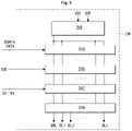
- FIG. 1 is a view illustrating a configuration of a liquid crystal display (LCD) device according to an embodiment of the present invention.
- LCD liquid crystal display
- the LCD device includes a liquid crystal panel 100, a timing controller 210, a power module 220, a gate driver 230, and a data driver 240.
- the liquid crystal panel 100 includes a thin film transistor (TFT) array substrate in which a TFT array is formed and a color filter substrate in which color filters are formed, and a liquid crystal layer is formed between the TFT array substrate and the color filter substrate.
- TFT thin film transistor
- a region of the TFT array substrate in which pixels P are arranged will be defined as a pixel array region 100A.
- pixels P defined by gate lines GL1 to GLm and data lines DL1 to DLn arranged horizontally and vertically, respectively, are arranged in a matrix form.
- a dummy data line DDL and compensation capacitors Cdc are formed to be parallel to the first data line DL1 on one side of the pixel array region 100A.
- the first data line DL1 may be an outermost data line of the data lines DL1 to DLn.
- the compensation capacitors Cdc may be arranged in a row parallel to the first data line DL1.
- the dummy data line DDL may be disposed between the compensation capacitors Cdc and the first data line DL1.
- a common line includes horizontal common lines VcomLl to VcomLm and one or more vertical common lines VcomLV.
- a common voltage Vcom generated by the power module 220 is supplied to a common electrode by way of the common line.
- the horizontal common lines VcomLl to VcomLm are disposed to be parallel to the gate lines GL1 to GLm.
- Each vertical common line VcomLV is disposed vertically in a position outside of the pixel array region 100A and connects the power module 220 and the horizontal common lines VcomLl to VcomLm.
- the vertical common line VcomLV and the horizontal common lines VcomLl to VcomLm may have a mesh form.
- a first vertical common line VcomLV may be disposed proximate the first data line DL1
- a second vertical common line VcomLV may be disposed proximate an n-th data line DLn.
- the n-th data line DLn may be an outermost data line disposed at a side of the pixel array region 100A which is opposite to the side of the pixel array region 100A where the first data line DL1 is disposed.
- Each compensation capacitor Cdc is formed in a position outside of the pixel array region 100A. Details of a structure and a function of the compensation capacitors Cdc will be described hereinafter.
- the dummy data line DDL is formed outside of the pixel array region 100A and receives a compensation data voltage ADDATA from the data driver 240.
- the timing controller 210 receives digital video data RGB from an external device (e.g., host) (not shown), and receives timing signals such as a vertical synchronization signal Vsync, a horizontal synchronization signal Hsync, a data enable signal Data Enable (DE), and a main clock CLK.
- the timing controller 210 transmits the digital video data RGB as digital video data DATA to source drive ICs of the data driver 240.
- the timing controller 210 generates a source timing control signal for controlling an operation timing of the data driver 240 and a gate timing control signal GCLK for controlling an operation timing of the gate driver 230 by using the timing signals Vsync, Hsync, DE, and CLK.
- the timing controller 210 generates compensation data DDATA provided to the dummy data line DDL.
- the compensation data DDATA is output as a compensation data voltage ADDATA through the data driver 240.
- the compensation data voltage is charged in a compensation capacitor Cdc to suppress ripples of the common voltage Vcom. Details thereof will be described hereinafter.
- the power module 220 receives a source voltage VCC and outputs a gate high voltage VGH, a gate low voltage VGL, a high potential voltage VDD, and the common voltage Vcom.
- the gate high voltage VGH is a high level voltage of a scan pulse supplied to a gate line GL
- the gate low voltage VGL is a low level voltage of a scan pulse supplied to the gate line GL.
- the common voltage Vcom may have a voltage level within a range from a low potential voltage to a high potential voltage VDD, and for example, the common voltage may have a voltage level of a middle level potential voltage HVDD between the low potential voltage and the high potential voltage VDD.
- the gate-in-panel(GIP)-type gate driver 230 includes a level shifter 231 and a shift register 233 mounted on a printed circuit board (PCB) 200.
- the level shifter 231 receives a driving voltage such as the gate high voltage VGH or the gate low voltage VGL, receives a start signal ST and a gate clock signal GCLK from the timing controller 210, and outputs a start pulse VST and a clock signal CLK swung between the gate high voltage VGH and the gate low voltage VGL.
- the clock signals CLK output from the level shifter 231 are sequentially phase-shifted and transmitted to the shift register 233 formed in the display panel 100.
- the shift register 233 is connected to the gate lines GL of the display panel 100.
- the shift register 233 includes a plurality of dependently connected stages.
- the shift register 233 shifts the start pulse VST input from the level shifter 231 according to the clock signal CLK and sequentially supplies a gate pulse to the gate lines GL1 to GLm.
- the data driver 240 receives the digital video data DATA and compensation data DDATA from the timing controller 210. In response to a source timing control signal from the timing controller 210, the data driver 240 converts the digital video data DATA into a positive polarity/negative polarity analog data voltage and subsequently supplies the data voltage to the data lines DL1 to DLn of the display panel 100 such that the data voltage is synchronized with a gate pulse. The data driver 240 converts the (digital) compensation data DDATA into the (analog) compensation data voltage ADDATA and subsequently supplies the compensation data voltage ADDATA to the dummy data line DDL.
- the data driver 240 includes a register unit 241, a first latch 243, a second latch 245, a digital-to-analog converter (DAC) 247, and an output unit 249.
- DAC digital-to-analog converter
- the register unit 241 samples RGB digital video data bits of an input image using data control signals SSC and SSP provided from the timing controller 210, and provides the sampled bits to the first latch 243.
- the RGB digital video data bits are the bits of the digital video data DATA received from the timing controller 210.
- the register unit 241 provides the compensation data DDATA provided from the timing controller 210 to the first latch 243.
- the first latch 243 samples and latches the compensation data DDATA and the digital video data bits (of the digital video data DATA) according to a clock sequentially provided from the register unit 241, and simultaneously outputs the latched compensation data DDATA and digital video data DATA.
- the second latch 245 latches the compensation data DDATA and the digital video data DATA received from the first latch 243, and simultaneously outputs the latched compensation data DDATA and digital video data DATA in response to a source output enable signal SOE.
- the output unit 249 provides the analog compensation data voltage ADDATA output from the DAC 247 to the dummy data line DDL and provides the video data voltage ADATA to the data lines DL1 to DLn during a low logical period of the source output enable signal SOE.
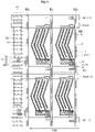
- FIG. 4 is a plan view illustrating pixels P and compensation capacitors Cdc
- FIG. 5 is a cross-sectional view taken along line I-I' of FIG. 4
- FIG. 6 is an equivalent circuit diagram of FIG. 4 .
- Gate lines GL(1) to GLm, horizontal common lines VcomLl to VcomLm, data lines DL1 to DLn, dummy data line DDL, and dummy common electrodes 13 are formed on a substrate.
- FIG. 4 shows four pixels P, (i-1)th to (i+1)th gate lines GL(i-1), GLi, GL(i+1), i-th and (i+1)th horizontal common lines VcomLi and VcomL(i+1), first and second data lines DL1 and DL2, dummy data line DDL, and two dummy common electrodes 13 associated with i-th horizontal common line VcomLi and (i+1)th horizontal common line VcomL(i+1), respectively.
- the data lines the gate lines according to their positions, the horizontal common lines, the data lines and the gate lines will be generally described as a horizontal common line VcomL, a data line DL and a gate line GL.
- the same components included in the pixels P or the compensation capacitors Cdc will also be described using the same reference numeral.
- Each horizontal common line VcomL is formed to be parallel to the gate line GL.
- the dummy common electrode 13 is formed to be perpendicular to the gate line GL.
- the dummy common electrode 13 is branched from one side of the horizontal common line VcomL and formed in a vertical direction.
- First gate electrodes 41 and at least one second gate electrode 42 branched in a vertical direction are formed on one side of the gate line GL.
- the at least one second gate electrode 42 is branched from the gate line GL outside of the pixel array region 100A.
- the gate line GL, the horizontal common line VcomL, and the dummy common electrode 13 may be formed of a gate metal material through the same process.
- a gate insulating layer GI is formed on the entire upper portion of the gate line GL, the horizontal common line VcomL, and the dummy common electrode 13.
- the data line DL, the dummy data line DDL, first and second drain electrodes 21 and 22, and first and second source electrodes 31 and 32 are formed on the gate insulating layer GI.
- the first drain electrode 21 is formed to protrude from the data line DL in a region where the first gate electrode 41 is positioned.
- the first source electrode 31 is formed to be adjacent to the first drain electrode 21.
- the first gate electrode 41, the first drain electrode 21, and the first source electrode 31 form a first transistor T1.
- the first transistor T1 In response to a gate pulse provided from the gate line GL, the first transistor T1 provides a data voltage provided from the data line DL to a pixel electrode 17.
- the dummy data line DDL includes the second drain electrode 22 protruding from a region where the second gate electrode 42 is positioned.
- the second source electrode 32 is formed to be adjacent to the second drain electrode 22.
- the second gate electrode 42, the second drain electrode 22, and the second source electrode 32 form a second transistor T2, and in response to a gate pulse provided from the gate line GL, the second transistor T2 provides a compensation data voltage provided from the dummy data line DDL to a conductive pattern 50.
- the conductive pattern 50 will be described as a metal pattern 50. However, the conductive pattern 50 may include or may be made of conductive materials other than metal.
- the second transistor T2 may be disposed outside the pixel array region 100A.
- an active layer e.g., a semiconductor layer
- a passivation layer PAS is formed on the data line DL, the dummy data line DDL, the first and second drain electrodes 21 and 22, and the first and second source electrodes 31 and 32.
- a pixel electrode 17, a common electrode 15, and the metal pattern 50 are formed on the passivation layer PAS.
- the pixel electrode 17, the liquid crystal layer, and the common electrode 15 form a liquid crystal capacitor Clc to display a gray level corresponding to a data voltage.
- the storage capacitor Cst stores a data signal during one frame to constantly maintain a voltage of the pixel electrode.
- the metal pattern 50 is formed to face the dummy common electrode 13, and the dummy common electrode 13 and the metal pattern 50 form the compensation capacitor Cdc with an insulating layer interposed therebetween.
- the compensation capacitor Cdc is charged to a compensation data voltage provided from the dummy data line DDL and cancels out ripples of the common voltage Vcom during the process of charging the compensation data voltage.
- FIG. 7 is a timing diagram illustrating a change in polarity of a data voltage and an output of a compensation data voltage corresponding thereto.
- a first data voltage Adata A and a second data voltage Adata B are data voltages provided to data lines DL in columns adjacent to each other. Polarities of the first and second data voltages Adata A and Adata B are maintained during a polarity maintaining interval and reversed during a polarity change interval of a next polarity period.
- a solid line is a timing diagram illustrating common voltage Vcom according to the embodiment of the invention, and a dashed line is a timing diagram illustrating common voltage Vcom according to the related art.
- the compensation data voltage ADDATA starts to be output at a point in time at which the polarities of the first and second data voltages Adata A and Adata B are changed, and rapidly rises to a predetermined level.
- the compensation data voltage ADDATA which has risen to a preset maximum voltage level, gradually falls until before the polarities start to be changed.
- the compensation data voltage ADDATA whose voltage level rapidly rises at a voltage change time rapidly charges a compensation capacitor Cdc. If the voltage level of the compensation data voltage ADDATA were rapidly lowered, negative polarity ripples might be generated in the common voltage. Therefore, in accordance with various embodiments, the voltage level of the compensation data voltage ADDATA slowly falls. For example, when a polarity of the data voltage (e.g., first data voltage AData B or second data voltage AData B) is reversed in every k-th horizontal period (k is a natural number ranging from 2 to m/2), a voltage level of the compensation data voltage ADDATA rapidly rises during a first horizontal period and gradually falls during subsequent k-1 horizontal periods, as shown in Fig.
- a polarity of the data voltage e.g., first data voltage AData B or second data voltage AData B
- k is a natural number ranging from 2 to m/2
- the compensation data voltage ADDATA whose voltage level rapidly rises during the rising interval is provided to the metal pattern 50.
- the compensation capacitor Cdc is charged with the compensation data voltage ADDATA as illustrated in FIG. 8 . Since the metal pattern 50 is charged by the positive polarity compensation data voltage ADDATA, a compensation current Ic is induced in a direction toward the dummy common electrode 13 from the metal pattern 50 in the compensation capacitor Cdc.
- the compensation current Ic induced during the process of charging the compensation capacitor Cdc flows to the common electrode 15 through the dummy common electrode 13. Thus, negative polarity ripples generated in the common electrode 15 are canceled out.
- the compensation data voltage ADDATA for canceling the ripples is set such that a voltage level thereof is significantly changed during a short period of time. That is, a minimum voltage level min and a maximum voltage level max of the compensation data voltage ADDATA may be set as the lowest value and the highest value of the data voltage, respectively.
- the minimum voltage level min of the compensation data voltage ADDATA may be set to a voltage level corresponding to a gray level 0, and the maximum voltage level max may be set to a voltage level corresponding to a gray level 255.
- Capacitance of the compensation capacitor Cdc is equal to or greater than the sum of the liquid crystal capacitors Clc of the horizontal lines, and is set to equal to or less than 1.5 times the sum of the capacitances of the liquid crystal capacitors.
- the compensation capacitor Cdc cancels out ripples of the common electrode 15 using that the induced current within the compensation capacitor Cdc flows to the common electrode 15.
- capacitance of the compensation capacitor Cdc is equal to or greater than the sum of the capacitances of the liquid crystal capacitors.
- a maximum value of the capacitance of the compensation capacitor Cdc may be equal to or greater than the sum of the capacitances of the liquid crystal capacitors, and a maximum value thereof may vary according to design margins of the compensation capacitor Cdc.
- a maximum value of the capacitances of the compensation capacitors Cdc may be set to a value equal to or smaller than 1.5 times the sum of the capacitances of the liquid crystal capacitors.
- a polarity of the compensation data voltage ADDATA may be changed according to potentials of ripples of the common voltage Vcom, or may be maintained at a predetermined positive polarity voltage level as illustrated in FIG. 7 .
- the reason why the potential of the compensation data voltage ADDATA is maintained to have the positive polarity as illustrated in FIG. 7 is because the ripples of the common voltage Vcom mainly have a negative polarity.
- the ripples of the common voltage Vcom are proportional to a variation of voltage levels of the first and second data voltages Adata A and Adata B. That is, as illustrated in FIG.
- the moment polarities of the first and second data voltages Adata A and Adata B are changed from a positive polarity to a negative polarity, a voltage variation per unit time is large, and the moment polarities of the first and second data voltages Adata A and Adata B are changed from a negative polarity to a positive polarity, a voltage variation per unit time is small.
- ripples of the common voltage Vcom are severe the moment the polarities of the first and second data voltages Adata A and Adata B are changed to the negative polarity. Since the ripples of the common voltage Vcom are generated mainly as having a negative polarity, the compensation data voltage ADDATA constantly maintains a positive polarity voltage.
- a P buffer BUF_P outputting a positive polarity voltage may be connected to the dummy data line DDL as illustrated in (a) of FIG. 9 .
- a buffer unit 246 and the dummy data line DDL are connected using a multiplexer 248.
- the multiplexer 248 connects the P buffer BUF_P and the dummy data line DDL regardless of a first selection signal MUX1 or a second selection signal MUX2. So, the N buffer BUF_N is not connected to the dummy data line DDL.
- ripples generated in the common voltage Vcom are suppressed by using the compensation data voltage ADDATA charged in the compensation capacitor Cdc during the polarity change interval.
- the compensation data voltage ADDATA is switched by a gate pulse provided to each horizontal line so as to be supplied to the compensation capacitor Cdc, delay of the ripples of the common voltage Vcom may be reflected for compensation.
- the delay phenomenon of the ripples of the common voltage Vcom results from a delay phenomenon of the data voltage ADATA as illustrated in FIG. 10 .
- the data voltage ADATA is output from the data driver 240 and supplied from a first horizontal line HL1 (of pixels) to an mth horizontal line HLm (of pixels).
- a data voltage supplied to a jth horizontal line HLj (of pixels) positioned away from the data driver 240 is delayed by ⁇ t relative to a point in time at which the jth horizontal period jH starts due to the data delay phenomenon.
- the ripples of the common voltage Vcom are also delayed by ⁇ t.
- the compensation data voltage ADDATA is delayed by the same timing and synchronized with a timing at which the data voltage ADATA is provided to the pixel P by a gate pulse, so as to be provided to the compensation capacitor Cdc.
- the compensation capacitor Cdc may effectively suppress ripples of the common voltage Vcom in response to a timing at which the ripples of the common voltage Vcom are generated in each horizontal line.
- FIG. 11 is a view illustrating a planar structure of a TFT array substrate of a liquid crystal panel according to a second embodiment.
- pixels P defined by gate lines GL1 to GLm and data lines DL1 to DLm arranged horizontally and vertically, respectively, are arranged in a matrix form.
- a first dummy data line DDL1 and first compensation capacitors Cdcl are formed to be parallel to the first data line DL1 on one side of a pixel array region 100A.
- a second dummy data line DDL2 and second compensation capacitors Cdc2 are formed to be parallel to the nth data line DLn on the other side of the pixel array region 100A.
- the same reference numerals will be used for components substantially the same as those of the first embodiment and detailed descriptions thereof will be omitted.
- the first and second compensation capacitors Cdcl and Cdc2 have a dummy common electrode and a metal pattern 50 branched from each of the horizontal common lines VcomLl to VcomLm as an electrode pair, and are formed in positions outside of the pixel array region 100A.
- capacitances of the first and second compensation capacitors Cdcl and Cdc2 may be designed to be smaller than that of a case using a single compensation capacitor. That is, a design margin of the compensation capacitor Cdc may be secured.
Description
- This document relates to a liquid crystal display device.
- An active matrix driving type liquid crystal display displays video using a thin film transistor (TFT) as a switching element. Compared with cathode ray tubes (CRTs), the liquid crystal display may be reduced in size so as to be applied to display devices of portable information devices, office machines, computers, and the like, and also, applied to televisions, rapidly replacing CRTs.
- In a liquid crystal display, pixels are formed as data lines and gate lines intersect each other, and include thin film transistors (TFTs) connected to the intersections of the data lines and the gate lines. In response to a gate pulse from a gate line, each TFT supplies a data voltage supplied through a data line to a pixel electrode of a liquid crystal cell. Driven by an electric field generated according to a voltage difference between a voltage of a pixel electrode and a common voltage Vcom applied to a common electrode, the liquid crystal cell adjusts an amount of light passing through a polarizing plate. A storage capacitor is connected to the pixel electrode of the liquid crystal cell to maintain a voltage of the liquid crystal cell.
- The common voltage Vcom applied to the common electrode may cause a ripple phenomenon due to electrical coupling with the pixel electrode. The ripple phenomenon of the common voltage Vcom is proportional to variations of a data voltage over time. Thus, in an inversion scheme driven by varying the polarity of the data voltage, a variation of the data voltage is so large that the ripple phenomenon of the common voltage Vcom becomes severe the moment a polarity of the data voltage is changed. The ripple phenomenon of the common voltage Vcom causes a line dim phenomenon in a horizontal direction, degrading display quality.
-
US 5 946 068 A describes dummy LCD elements receiving instead of the normal data signals for the other true LCD elements a corresponding dummy data signal. The polarity of that dummy data signal is inverted with respect to the polarity of the data signal driving the data line connected to the LCD elements of the outermost column of true LCD elements in line with the dot inversion technique to drive the LCD elements. -
US 2008/0094388 A1 describes that the common signal output circuit buffers the reference voltage in a first period when a period for selecting the scanning line starts, and output the common signal for performing feedback control such that the voltage of the common electrode becomes the reference voltage, in a second period when a period for selecting the scanning line is finished. -
US 2014/0176839 A1 describes to generate a current common voltage data supplied to a common electrode by using previous common voltage data and a feedback common voltage that is outputted to the common electrode by the previous common voltage data and fed back therefrom. - Patent application
US 2008/291144 A1 describes a liquid crystal display with a common voltage modulator to keep the common voltage of the LCD stable by receiving a distorted common voltage from the common electrode via a first common voltage line and applying a corresponding compensating voltage to the common electrode via a second common voltage line being also connected to the common electrode. - Patent application
US 2004/196241 A1 describes replacing a common electrode with a plurality of switch electrodes grouped in sets, where each set is modulated by a different driving circuit, in order to reduce electrical power consumption. - Patent application
US 2006/244704 A1 describes a liquid crystal display in which a distortion of the common voltage across the entire region of the liquid crystal is prevented by a first and a second common voltage compensator supplying a first and a second common voltage supply lines, respectively, where the first and second common voltage supply lines are spaced apart and positioned near the edges of the liquid crystal panel. - Patent applications
EP 2 182 508 A1 ,US 2007/206136 A1 ,US 2008/278471 A1 , andUS 2008/117148 A1 describe further display devices. - The invention is defined in
claims 1 and 10. - In one or more embodiments, the at least one compensation capacitor comprises a first compensation capacitor and a second compensation capacitor, wherein the first and second compensation capacitors are arranged at opposite sides of a pixel array region, in which the pixels are arranged.
- In one or more embodiments, each pixel comprises: a pixel electrode, and a liquid crystal capacitor formed by the pixel electrode, the common electrode and a liquid crystal layer disposed between the pixel electrode and the common electrode; wherein a capacitance of a compensation capacitor coupled to a horizontal common line is equal to or greater than the sum of capacitances of liquid crystal capacitors coupled to said horizontal common line. The capacitance of the compensation capacitor coupled to said horizontal common line may be less than or equal to 1.5 times the sum of the capacitances of the liquid crystal capacitors coupled to said horizontal common line.
- In one or more embodiments, the data driver is configured to increase a level of the compensation data voltage from a predetermined minimum voltage level to a predetermined maximum voltage level during a polarity change interval, in which the polarity of the data voltage is changed from the first polarity to the second polarity, and decrease the level of the compensation data voltage from the predetermined maximum level to the predetermined minimum level during a subsequent polarity maintaining interval, in which the polarity of the data voltage is maintained at the second polarity, wherein the polarity maintaining interval is longer than the polarity change interval. A length of the polarity change interval may be equal to one horizontal driving period and a length of the polarity maintaining interval may be equal to two or more horizontal driving periods.
- In one or more embodiments, the predetermined minimum voltage level and the predetermined maximum voltage level of the compensation data voltage are set equal to a lowest possible value and a highest possible value of the data voltage, respectively.
- In one or more embodiments, the liquid crystal display device further comprises: a gate driver; a plurality of gate lines and data lines arranged in the direction of the rows and columns, respectively, and coupled to the gate driver and the data driver, respectively, to receive a gate pulse and the data voltage, respectively; at least one dummy data line arranged in parallel with the data lines and coupled to the data driver to receive the compensation data voltage; wherein each pixel comprises a switching transistor coupled to a respective gate line and data line and configured to supply the data voltage from the data driver to a pixel electrode of the pixel upon applying the gate pulse from the gate driver to the gate line; wherein each row comprises at least one additional switching transistor coupled to the at least one dummy data line, to a compensation capacitor corresponding to that row, and to a gate line coupled to the switching transistors of the pixels in that row, wherein the at least one additional switching transistor is configured to supply the compensation data voltage from the data driver to the compensation capacitor upon applying the gate pulse from the gate driver to the gate line. The at least one dummy data line may be arranged outside a pixel array region, in which the pixels are arranged.
- In one or more embodiments, the timing controller is configured to synchronize the timing of the compensation data voltage with a timing of the data voltage so as to provide the compensation data voltage with the same time delay to a compensation capacitor corresponding to a row as the data voltage is provided to a pixel in that row. In one or more embodiments, the timing controller is configured to receive digital video data and timing signals.
- In one or more embodiments, the timing controller is configured to transmit the digital video data to source drive ICs of the data driver.
- In one or more embodiments, the timing controller is configured to generate a source timing control signal for controlling an operation timing of the data driver and a gate timing control signal for controlling an operation timing of the gate driver by using the timing signals.
- In one or more embodiments, the power module is configured to receive a source voltage and output a gate high voltage, a gate low voltage, a high potential voltage, and the common voltage.
- In one or more embodiments, the gate driver comprises a level shifter connected to the timing controller, and a shift register connected between the level shifter and the gate lines.
- In one or more embodiments, the horizontal common lines and the at least one vertical common line have a mesh form.
- In one or more embodiments, the compensation data voltage has a positive polarity.
- In one or more embodiments, the polarity maintaining interval immediately follows the polarity change interval.
- In one or more embodiments, charging the compensation data voltage into the compensation capacitor comprises: increasing a level of the compensation data voltage from a predetermined minimum voltage level to a predetermined maximum voltage level during a polarity change interval, in which the polarity of the data voltage is changed from the first polarity to the second polarity.
- In one or more embodiments, the method further comprises: decreasing the level of the compensation data voltage from the predetermined maximum level to the predetermined minimum level during a polarity maintaining interval, in which the polarity of the data voltage is maintained at the second polarity, subsequent to the polarity change interval, wherein the polarity maintaining interval is longer than the polarity change interval. A length of the polarity change interval may be equal to one horizontal driving period and a length of the polarity maintaining interval may be equal to two or more horizontal driving periods.
- In one or more embodiments, the method further comprises: synchronizing the timing of the compensation data voltage with a timing of the data voltage so as to provide the compensation data voltage with the same time delay to a compensation capacitor corresponding to a row as the data voltage is provided to a pixel in that row.
- In one or more embodiments, the first polarity is a positive polarity and the second polarity is a negative polarity, and the compensation data voltage has a positive polarity.
- The accompanying drawings, which are included to provide a further understanding of the invention and are incorporated in and constitute a part of this specification, illustrate embodiments of the invention and together with the description serve to explain the principles of the invention. In the drawings:
-
FIG. 1 is a view illustrating a configuration of a liquid crystal display (LCD) device according to an embodiment of the present invention. -
FIG. 2 is a view illustrating a pixel array region according to a first embodiment. -
FIG. 3 is a view illustrating a configuration of a data driver according to an embodiment of the present invention. -
FIG. 4 is a view illustrating a planar structure of pixels and compensation capacitors. -
FIG. 5 is a cross-sectional view taken along line I-I' ofFIG. 4 . -
FIG. 6 is an equivalent circuit diagram of the pixels and the compensation capacitors ofFIG. 4 . -
FIG. 7 is a view illustrating timing of a data voltage and a compensation data voltage. -
FIG. 8 is a view illustrating a ripple cancelation phenomenon of a common voltage. -
FIGS. 9(a) and 9(b) are views illustrating an embodiment of an output buffer outputting a compensation data voltage. -
FIG. 10 is a view illustrating ripple cancelation of a common voltage by reflecting data voltage delay. -
FIG. 11 is a view illustrating a pixel array region according to a second embodiment. - Hereinafter, embodiments will be described in detail with reference to the accompanying drawings. Throughout the specification, the like reference numerals denote the substantially same elements. In describing the present invention, if a detailed explanation for a related known function or construction is considered to unnecessarily divert the gist of the present invention, such explanation will be omitted but would be understood by those skilled in the art.
- Names of elements used in the following description are selected for the description purpose and may be different from those of actual products.
-
FIG. 1 is a view illustrating a configuration of a liquid crystal display (LCD) device according to an embodiment of the present invention. - Referring to
FIG. 1 , the LCD device according to an embodiment of the present invention includes aliquid crystal panel 100, atiming controller 210, apower module 220, agate driver 230, and adata driver 240. - The
liquid crystal panel 100 includes a thin film transistor (TFT) array substrate in which a TFT array is formed and a color filter substrate in which color filters are formed, and a liquid crystal layer is formed between the TFT array substrate and the color filter substrate. In theliquid crystal panel 100, a region of the TFT array substrate in which pixels P are arranged will be defined as apixel array region 100A. - As illustrated in
FIG. 2 , in the TFT array substrate of theliquid crystal panel 100 according to a first embodiment, pixels P defined by gate lines GL1 to GLm and data lines DL1 to DLn arranged horizontally and vertically, respectively, are arranged in a matrix form. A dummy data line DDL and compensation capacitors Cdc are formed to be parallel to the first data line DL1 on one side of thepixel array region 100A. The first data line DL1 may be an outermost data line of the data lines DL1 to DLn. The compensation capacitors Cdc may be arranged in a row parallel to the first data line DL1. The dummy data line DDL may be disposed between the compensation capacitors Cdc and the first data line DL1. - A common line includes horizontal common lines VcomLl to VcomLm and one or more vertical common lines VcomLV. A common voltage Vcom generated by the
power module 220 is supplied to a common electrode by way of the common line. The horizontal common lines VcomLl to VcomLm are disposed to be parallel to the gate lines GL1 to GLm. Each vertical common line VcomLV is disposed vertically in a position outside of thepixel array region 100A and connects thepower module 220 and the horizontal common lines VcomLl to VcomLm. The vertical common line VcomLV and the horizontal common lines VcomLl to VcomLm may have a mesh form. In an embodiment, a first vertical common line VcomLV may be disposed proximate the first data line DL1, and a second vertical common line VcomLV may be disposed proximate an n-th data line DLn. The n-th data line DLn may be an outermost data line disposed at a side of thepixel array region 100A which is opposite to the side of thepixel array region 100A where the first data line DL1 is disposed. - Each compensation capacitor Cdc is formed in a position outside of the
pixel array region 100A. Details of a structure and a function of the compensation capacitors Cdc will be described hereinafter. - The dummy data line DDL is formed outside of the
pixel array region 100A and receives a compensation data voltage ADDATA from thedata driver 240. - The
timing controller 210 receives digital video data RGB from an external device (e.g., host) (not shown), and receives timing signals such as a vertical synchronization signal Vsync, a horizontal synchronization signal Hsync, a data enable signal Data Enable (DE), and a main clock CLK. Thetiming controller 210 transmits the digital video data RGB as digital video data DATA to source drive ICs of thedata driver 240. Thetiming controller 210 generates a source timing control signal for controlling an operation timing of thedata driver 240 and a gate timing control signal GCLK for controlling an operation timing of thegate driver 230 by using the timing signals Vsync, Hsync, DE, and CLK. - Also, the
timing controller 210 generates compensation data DDATA provided to the dummy data line DDL. The compensation data DDATA is output as a compensation data voltage ADDATA through thedata driver 240. The compensation data voltage is charged in a compensation capacitor Cdc to suppress ripples of the common voltage Vcom. Details thereof will be described hereinafter. - The
power module 220 receives a source voltage VCC and outputs a gate high voltage VGH, a gate low voltage VGL, a high potential voltage VDD, and the common voltage Vcom. The gate high voltage VGH is a high level voltage of a scan pulse supplied to a gate line GL, and the gate low voltage VGL is a low level voltage of a scan pulse supplied to the gate line GL. The common voltage Vcom may have a voltage level within a range from a low potential voltage to a high potential voltage VDD, and for example, the common voltage may have a voltage level of a middle level potential voltage HVDD between the low potential voltage and the high potential voltage VDD. - The gate-in-panel(GIP)-
type gate driver 230 includes alevel shifter 231 and ashift register 233 mounted on a printed circuit board (PCB) 200. - The
level shifter 231 receives a driving voltage such as the gate high voltage VGH or the gate low voltage VGL, receives a start signal ST and a gate clock signal GCLK from thetiming controller 210, and outputs a start pulse VST and a clock signal CLK swung between the gate high voltage VGH and the gate low voltage VGL. The clock signals CLK output from thelevel shifter 231 are sequentially phase-shifted and transmitted to theshift register 233 formed in thedisplay panel 100. - The
shift register 233 is connected to the gate lines GL of thedisplay panel 100. Theshift register 233 includes a plurality of dependently connected stages. Theshift register 233 shifts the start pulse VST input from thelevel shifter 231 according to the clock signal CLK and sequentially supplies a gate pulse to the gate lines GL1 to GLm. - The
data driver 240 receives the digital video data DATA and compensation data DDATA from thetiming controller 210. In response to a source timing control signal from thetiming controller 210, thedata driver 240 converts the digital video data DATA into a positive polarity/negative polarity analog data voltage and subsequently supplies the data voltage to the data lines DL1 to DLn of thedisplay panel 100 such that the data voltage is synchronized with a gate pulse. Thedata driver 240 converts the (digital) compensation data DDATA into the (analog) compensation data voltage ADDATA and subsequently supplies the compensation data voltage ADDATA to the dummy data line DDL. - To this end, as illustrated in
FIG. 3 , thedata driver 240 includes aregister unit 241, afirst latch 243, asecond latch 245, a digital-to-analog converter (DAC) 247, and anoutput unit 249. - The
register unit 241 samples RGB digital video data bits of an input image using data control signals SSC and SSP provided from thetiming controller 210, and provides the sampled bits to thefirst latch 243. The RGB digital video data bits are the bits of the digital video data DATA received from thetiming controller 210. Also, theregister unit 241 provides the compensation data DDATA provided from thetiming controller 210 to thefirst latch 243. - The
first latch 243 samples and latches the compensation data DDATA and the digital video data bits (of the digital video data DATA) according to a clock sequentially provided from theregister unit 241, and simultaneously outputs the latched compensation data DDATA and digital video data DATA. Thesecond latch 245 latches the compensation data DDATA and the digital video data DATA received from thefirst latch 243, and simultaneously outputs the latched compensation data DDATA and digital video data DATA in response to a source output enable signal SOE. - The
DAC 247 converts the compensation data DDATA and digital video data DATA received from thesecond latch 245 into a gamma compensation voltage GMA using or based on gamma voltages G1 to Gm (e.g., m analog voltage levels G1 to Gm; for example m = 255) to generate an analog compensation data voltage ADDATA and a video data voltage ADATA. - The
output unit 249 provides the analog compensation data voltage ADDATA output from theDAC 247 to the dummy data line DDL and provides the video data voltage ADATA to the data lines DL1 to DLn during a low logical period of the source output enable signal SOE. -
FIG. 4 is a plan view illustrating pixels P and compensation capacitors Cdc,FIG. 5 is a cross-sectional view taken along line I-I' ofFIG. 4 , andFIG. 6 is an equivalent circuit diagram ofFIG. 4 . - The configuration of the compensation capacitors Cdc and the pixels P will be described with reference to
FIGS. 4 through 6 . Gate lines GL(1) to GLm, horizontal common lines VcomLl to VcomLm, data lines DL1 to DLn, dummy data line DDL, and dummycommon electrodes 13 are formed on a substrate. As an example,Fig. 4 shows four pixels P, (i-1)th to (i+1)th gate lines GL(i-1), GLi, GL(i+1), i-th and (i+1)th horizontal common lines VcomLi and VcomL(i+1), first and second data lines DL1 and DL2, dummy data line DDL, and two dummycommon electrodes 13 associated with i-th horizontal common line VcomLi and (i+1)th horizontal common line VcomL(i+1), respectively. In the following descriptions, when it is not necessary to distinguish between the horizontal common lines, the data lines the gate lines according to their positions, the horizontal common lines, the data lines and the gate lines will be generally described as a horizontal common line VcomL, a data line DL and a gate line GL. Also, the same components included in the pixels P or the compensation capacitors Cdc will also be described using the same reference numeral. - Each horizontal common line VcomL is formed to be parallel to the gate line GL. The dummy
common electrode 13 is formed to be perpendicular to the gate line GL. The dummycommon electrode 13 is branched from one side of the horizontal common line VcomL and formed in a vertical direction.First gate electrodes 41 and at least onesecond gate electrode 42 branched in a vertical direction are formed on one side of the gate line GL. The at least onesecond gate electrode 42 is branched from the gate line GL outside of thepixel array region 100A. The gate line GL, the horizontal common line VcomL, and the dummycommon electrode 13 may be formed of a gate metal material through the same process. - A gate insulating layer GI is formed on the entire upper portion of the gate line GL, the horizontal common line VcomL, and the dummy
common electrode 13. - The data line DL, the dummy data line DDL, first and
second drain electrodes second source electrodes - The
first drain electrode 21 is formed to protrude from the data line DL in a region where thefirst gate electrode 41 is positioned. Thefirst source electrode 31 is formed to be adjacent to thefirst drain electrode 21. Thefirst gate electrode 41, thefirst drain electrode 21, and thefirst source electrode 31 form a first transistor T1. In response to a gate pulse provided from the gate line GL, the first transistor T1 provides a data voltage provided from the data line DL to apixel electrode 17. - The dummy data line DDL includes the
second drain electrode 22 protruding from a region where thesecond gate electrode 42 is positioned. Thesecond source electrode 32 is formed to be adjacent to thesecond drain electrode 22. Thesecond gate electrode 42, thesecond drain electrode 22, and thesecond source electrode 32 form a second transistor T2, and in response to a gate pulse provided from the gate line GL, the second transistor T2 provides a compensation data voltage provided from the dummy data line DDL to aconductive pattern 50. In the following, theconductive pattern 50 will be described as ametal pattern 50. However, theconductive pattern 50 may include or may be made of conductive materials other than metal. - As shown in
Fig. 4 , the second transistor T2 may be disposed outside thepixel array region 100A. Furthermore, although not shown in the figures, an active layer (e.g., a semiconductor layer) may be provided between the gate insulating layer GI and the first source and drainelectrodes first gate electrode 41 to provide an electrically conductive channel between the first source and drainelectrodes electrodes second gate electrode 42 to provide an electrically conductive channel between the second source and drainelectrodes - A passivation layer PAS is formed on the data line DL, the dummy data line DDL, the first and
second drain electrodes second source electrodes - A
pixel electrode 17, acommon electrode 15, and themetal pattern 50 are formed on the passivation layer PAS. Thepixel electrode 17, the liquid crystal layer, and thecommon electrode 15 form a liquid crystal capacitor Clc to display a gray level corresponding to a data voltage. The storage capacitor Cst stores a data signal during one frame to constantly maintain a voltage of the pixel electrode. - The
metal pattern 50 is formed to face the dummycommon electrode 13, and the dummycommon electrode 13 and themetal pattern 50 form the compensation capacitor Cdc with an insulating layer interposed therebetween. The compensation capacitor Cdc is charged to a compensation data voltage provided from the dummy data line DDL and cancels out ripples of the common voltage Vcom during the process of charging the compensation data voltage. - A method for suppressing ripples of the common voltage Vcom by the compensation capacitor Cdc will be described.
-
FIG. 7 is a timing diagram illustrating a change in polarity of a data voltage and an output of a compensation data voltage corresponding thereto. - In
FIG. 7 , a first data voltage Adata A and a second data voltage Adata B are data voltages provided to data lines DL in columns adjacent to each other. Polarities of the first and second data voltages Adata A and Adata B are maintained during a polarity maintaining interval and reversed during a polarity change interval of a next polarity period. InFig.7 , a solid line is a timing diagram illustrating common voltage Vcom according to the embodiment of the invention, and a dashed line is a timing diagram illustrating common voltage Vcom according to the related art. - The compensation data voltage ADDATA starts to be output at a point in time at which the polarities of the first and second data voltages Adata A and Adata B are changed, and rapidly rises to a predetermined level. The compensation data voltage ADDATA, which has risen to a preset maximum voltage level, gradually falls until before the polarities start to be changed.
- The compensation data voltage ADDATA whose voltage level rapidly rises at a voltage change time rapidly charges a compensation capacitor Cdc. If the voltage level of the compensation data voltage ADDATA were rapidly lowered, negative polarity ripples might be generated in the common voltage. Therefore, in accordance with various embodiments, the voltage level of the compensation data voltage ADDATA slowly falls. For example, when a polarity of the data voltage (e.g., first data voltage AData B or second data voltage AData B) is reversed in every k-th horizontal period (k is a natural number ranging from 2 to m/2), a voltage level of the compensation data voltage ADDATA rapidly rises during a first horizontal period and gradually falls during subsequent k-1 horizontal periods, as shown in
Fig. 7 , which shows rising of the voltage level of ADDATA during a firsthorizontal period 1H and falling of the voltage level during k-1 subsequenthorizontal periods - The compensation data voltage ADDATA whose voltage level rapidly rises during the rising interval is provided to the
metal pattern 50. When themetal pattern 50 receives the compensation data voltage ADDATA, the compensation capacitor Cdc is charged with the compensation data voltage ADDATA as illustrated inFIG. 8 . Since themetal pattern 50 is charged by the positive polarity compensation data voltage ADDATA, a compensation current Ic is induced in a direction toward the dummycommon electrode 13 from themetal pattern 50 in the compensation capacitor Cdc. The compensation current Ic induced during the process of charging the compensation capacitor Cdc flows to thecommon electrode 15 through the dummycommon electrode 13. Thus, negative polarity ripples generated in thecommon electrode 15 are canceled out. - Since the ripples generated in the
common electrode 15 are instantaneously generated during a period in which the polarities of the first and second data voltages Adata A and Adata B are changed, the compensation data voltage ADDATA for canceling the ripples is set such that a voltage level thereof is significantly changed during a short period of time. That is, a minimum voltage level min and a maximum voltage level max of the compensation data voltage ADDATA may be set as the lowest value and the highest value of the data voltage, respectively. For example, the minimum voltage level min of the compensation data voltage ADDATA may be set to a voltage level corresponding to a gray level 0, and the maximum voltage level max may be set to a voltage level corresponding to a gray level 255. - Capacitance of the compensation capacitor Cdc is equal to or greater than the sum of the liquid crystal capacitors Clc of the horizontal lines, and is set to equal to or less than 1.5 times the sum of the capacitances of the liquid crystal capacitors. As described above, the compensation capacitor Cdc cancels out ripples of the
common electrode 15 using that the induced current within the compensation capacitor Cdc flows to thecommon electrode 15. Thus, in order to supply a compensation current Ic to every pixel P connected to one horizontal line, capacitance of the compensation capacitor Cdc is equal to or greater than the sum of the capacitances of the liquid crystal capacitors. A maximum value of the capacitance of the compensation capacitor Cdc may be equal to or greater than the sum of the capacitances of the liquid crystal capacitors, and a maximum value thereof may vary according to design margins of the compensation capacitor Cdc. For example, a maximum value of the capacitances of the compensation capacitors Cdc may be set to a value equal to or smaller than 1.5 times the sum of the capacitances of the liquid crystal capacitors. - A polarity of the compensation data voltage ADDATA may be changed according to potentials of ripples of the common voltage Vcom, or may be maintained at a predetermined positive polarity voltage level as illustrated in
FIG. 7 . The reason why the potential of the compensation data voltage ADDATA is maintained to have the positive polarity as illustrated inFIG. 7 is because the ripples of the common voltage Vcom mainly have a negative polarity. The ripples of the common voltage Vcom are proportional to a variation of voltage levels of the first and second data voltages Adata A and Adata B. That is, as illustrated inFIG. 7 , the moment polarities of the first and second data voltages Adata A and Adata B are changed from a positive polarity to a negative polarity, a voltage variation per unit time is large, and the moment polarities of the first and second data voltages Adata A and Adata B are changed from a negative polarity to a positive polarity, a voltage variation per unit time is small. Thus, ripples of the common voltage Vcom are severe the moment the polarities of the first and second data voltages Adata A and Adata B are changed to the negative polarity. Since the ripples of the common voltage Vcom are generated mainly as having a negative polarity, the compensation data voltage ADDATA constantly maintains a positive polarity voltage. - In order to maintain the potential of the compensation data voltage ADDATA as having a positive polarity, in an output buffer outputting the compensation data voltage ADDATA to the dummy data line DDL, only a P buffer BUF_P outputting a positive polarity voltage may be connected to the dummy data line DDL as illustrated in (a) of
FIG. 9 . In (b) ofFig. 9 , abuffer unit 246 and the dummy data line DDL are connected using amultiplexer 248. Themultiplexer 248 connects the P buffer BUF_P and the dummy data line DDL regardless of a first selection signal MUX1 or a second selection signal MUX2. So, the N buffer BUF_N is not connected to the dummy data line DDL. As described above, in the LCD device according to an embodiment of the present invention, ripples generated in the common voltage Vcom are suppressed by using the compensation data voltage ADDATA charged in the compensation capacitor Cdc during the polarity change interval. In particular, since the compensation data voltage ADDATA is switched by a gate pulse provided to each horizontal line so as to be supplied to the compensation capacitor Cdc, delay of the ripples of the common voltage Vcom may be reflected for compensation. - The delay phenomenon of the ripples of the common voltage Vcom results from a delay phenomenon of the data voltage ADATA as illustrated in
FIG. 10 . The data voltage ADATA is output from thedata driver 240 and supplied from a first horizontal line HL1 (of pixels) to an mth horizontal line HLm (of pixels). A data voltage supplied to a jth horizontal line HLj (of pixels) positioned away from thedata driver 240 is delayed by △t relative to a point in time at which the jth horizontal period jH starts due to the data delay phenomenon. Thus, the ripples of the common voltage Vcom are also delayed by △t. - In the LCD device according to an embodiment of the present invention, the compensation data voltage ADDATA is delayed by the same timing and synchronized with a timing at which the data voltage ADATA is provided to the pixel P by a gate pulse, so as to be provided to the compensation capacitor Cdc. Thus, the compensation capacitor Cdc may effectively suppress ripples of the common voltage Vcom in response to a timing at which the ripples of the common voltage Vcom are generated in each horizontal line.
-
FIG. 11 is a view illustrating a planar structure of a TFT array substrate of a liquid crystal panel according to a second embodiment. - Referring to
FIG. 11 , in the TFT array substrate of aliquid crystal panel 100 according to the second embodiment, pixels P defined by gate lines GL1 to GLm and data lines DL1 to DLm arranged horizontally and vertically, respectively, are arranged in a matrix form. A first dummy data line DDL1 and first compensation capacitors Cdcl are formed to be parallel to the first data line DL1 on one side of apixel array region 100A. Also, a second dummy data line DDL2 and second compensation capacitors Cdc2 are formed to be parallel to the nth data line DLn on the other side of thepixel array region 100A. In the second embodiment, the same reference numerals will be used for components substantially the same as those of the first embodiment and detailed descriptions thereof will be omitted. - The first and second compensation capacitors Cdcl and Cdc2 have a dummy common electrode and a
metal pattern 50 branched from each of the horizontal common lines VcomLl to VcomLm as an electrode pair, and are formed in positions outside of thepixel array region 100A. In the second embodiment, since the first and second compensation capacitors Cdcl and Cdc2 are formed on both sides of thepixel array region 100A, capacitances of the first and second compensation capacitors Cdcl and Cdc2 may be designed to be smaller than that of a case using a single compensation capacitor. That is, a design margin of the compensation capacitor Cdc may be secured. - In this manner, since ripples of the common voltage are canceled out by a compensation voltage generated when the compensation capacitor is charged, a line-dim phenomenon due to ripples of the common voltage may be improved.
Claims (14)
- A liquid crystal display device, comprising:a plurality of pixels (P) arranged in rows and columns in a matrix form;a plurality of m horizontal common lines (VcomLl, ..., VcomLm) arranged in the direction of the rows and coupled to a common electrode (15) of the plurality of pixels; and at least one vertical common line (VcomLV) arranged in the direction of the columns and connecting the m horizontal common lines (VcomLl, ..., VcomLm) to one another; a vertical dummy data line (DDL);a power module (220) configured to supply a common voltage (Vcom) to the at least one vertical common line common line (VcomL);at least one compensation capacitor (Cdc) comprising a conductive pattern (50), a dummy common electrode (13) coupled to a respective horizontal common line (VcomLi) and an insulating layer disposed between the dummy common electrode (13) and the conductive pattern (50);a data driver (240) coupled by means of the vertical dummy data line (DDL) to the conductive pattern (50) of the at least one compensation capacitor (Cdc), the data driver (240) being configured to:apply a data voltage (ADATA) having a first polarity to a pixel (P) of the plurality of pixels (P);subsequently change the polarity of the data voltage (ADATA) from the first polarity to a second polarity; andapply an analog compensation data voltage (ADDATA) by means of the vertical dummy data line (DDL) into the at least one compensation capacitor (Cdc) while changing the polarity of the data voltage (ADATA) from the first polarity to the second polarity, so as to reduce ripples in a common voltage (Vcom) applied to the horizontal common lines (VcomLl, ..., VcomLm);the liquid crystal display device further comprising:a timing controller (210) configured to generate a digital compensation data (DDATA) and provide the digital compensation data (DDATA) to the data driver (240),wherein the data driver (240) is configured to convert the digital compensation data (DDATA) into the analog compensation data voltage (ADDATA).
- The liquid crystal display device of claim 1, comprising:m compensation capacitors (Cdc), each of the m compensation capacitors being coupled to a respective horizontal common line (VcomLi),wherein the at least one vertical common line (VcomLV) is arranged outside a pixel array region (100A), in which the pixels (P) are arranged.
- The liquid crystal display device of claim 2, wherein each of the m compensation capacitors (Cdc) comprises:a respective dummy common electrode (13) that branches from the respective horizontal common line (VcomLi),a respective conductive pattern (50) that faces the dummy common electrode (13), anda respective insulating layer disposed between the dummy common electrode (13) and the conductive pattern (50) .
- The liquid crystal display device of claim 2 or 3, wherein each of the m compensation capacitors (Cdc) comprises a first compensation capacitor (Cdcl) and a second compensation capacitor (Cdc2), wherein the first and second compensation capacitors (Cdcl, Cdc2) are arranged at opposite sides of a pixel array region (100A), in which the pixels (P) are arranged.
- The liquid crystal display device of any one of claims 2 to 4, wherein each pixel (P) comprises:a pixel electrode (17), and a liquid crystal capacitor (Clc) formed by the pixel electrode (17), the common electrode (15) and a liquid crystal layer disposed between the pixel electrode (17) and the common electrode (15) ;wherein a capacitance of a compensation capacitor (CdC) coupled to a horizontal common line (VcomL) is equal to or greater than the sum of capacitances of liquid crystal capacitors (Clc) coupled to said horizontal common line (VcomL),wherein, preferably, the capacitance of the compensation capacitor (Cdc) coupled to said horizontal common line (VcomL) is less than or equal to 1.5 times the sum of the capacitances of the liquid crystal capacitors (Clc) coupled to said horizontal common line (VcomL).
- The liquid crystal display device of any one of claims 1 to 5,wherein the analog compensation data voltage (ADDATA) rises from a predetermined minimum voltage level to a predetermined maximum voltage level during a polarity change interval, starting at a point in time at which the polarity of the data voltage (ADATA) is changed from the first polarity to the second polarity, and decrease the level of the compensation data voltage (ADDATA) from the predetermined maximum level to the predetermined minimum level during a subsequent polarity maintaining interval, in which the polarity of the data voltage (ADATA) is maintained at the second polarity,wherein the polarity maintaining interval is longer than the polarity change interval,wherein, preferably, a length of the polarity change interval is equal to one horizontal driving period and a length of the polarity maintaining interval is equal to two or more horizontal driving periods.
- The liquid crystal display device of claim 6, wherein the predetermined minimum voltage level and the predetermined maximum voltage level of the analog compensation data voltage (ADDATA) are set equal to a lowest possible value and a highest possible value of the data voltage (ADATA), respectively.
- The liquid crystal display device of any one of claims 2 to 7, further comprising:a gate driver (230);a plurality of gate lines (GL1 to GLm) and data lines (DL to DLn) arranged in the direction of the rows and columns, respectively, and coupled to the gate driver (230) and the data driver (240), respectively, to receive a gate pulse and the data voltage (ADATA), respectively;the at least one vertical dummy data line (DDL) is arranged in parallel with the data lines (DL1, ..., DLn) and coupled to the data driver (240) to receive the analog compensation data voltage (ADDATA);wherein each pixel (P) comprises a switching transistor coupled to a respective gate line (GL1 to GLm) and data line and configured to supply the data voltage (ADATA) from the data driver (240) to a pixel electrode (17) of the pixel (P) upon applying the gate pulse from the gate driver (230) to the gate line (GL1 to GLm);wherein each row comprises at least one additional switching transistor coupled to the at least one vertical dummy data line (DDL), to a compensation capacitor (Cdc) corresponding to that row, and to a gate line (GL1 to GLm) coupled to the switching transistors of the pixels (P) in that row, wherein the at least one additional switching transistor is configured to supply the analog compensation data voltage (ADDATA) from the data driver (240) to the compensation capacitor (Cdc) upon applying the gate pulse from the gate driver (230) to the gate line (GL1 to GLm),wherein, preferably, the at least one vertical dummy data line (DDL) is arranged outside a pixel array region (100A), in which the pixels (P) are arranged.
- The liquid crystal display device of claim 8, wherein the timing controller (210) is configured to synchronize the timing of the compensation data voltage (ADDATA) with a timing of the data voltage (ADATA) so as to provide the compensation data voltage (ADDATA) with the same time delay to a compensation capacitor (Cdc) corresponding to a row as the data voltage (ADATA) is provided to a pixel (P) in that row.
- A method of driving a liquid crystal display device as defined in claim 1, the method comprising:generating digital compensation data (DDATA) by the timing controller (210);converting the digital compensation data (DDATA) into analog compensation data voltage (ADDATA) by the data driver (240);applying a data voltage (ADATA) having a first polarity to a pixel (P) of the plurality of pixels (P) by the data driver (240);subsequently changing the polarity of the data voltage (ADATA) from the first polarity to a second polarity by the data driver (240); andapplying the analog compensation data voltage (ADDATA) to the conductive pattern (50) of the at least one compensation capacitor (Cdc) coupled to the respective horizontal common line (VcomLi) by means of the vertical dummy data line (DDL) while changing the polarity of the data voltage (ADATA) from the first polarity to the second polarity, so as to charge the at least one compensation capacitor (Cdc) by the compensation data voltage (ADDATA) to reduce ripples in the common voltage (Vcom) applied to the horizontal common lines (VcomLl, VcomL2, ... VcomLm) .
- The method of claim 10, wherein charging the analog compensation data voltage (ADDATA) into the at least one compensation capacitor (Cdc) comprises:
increasing a level of the analog compensation data voltage (ADDATA) from a predetermined minimum voltage level to a predetermined maximum voltage level during a polarity change interval, starting at a point in time at which the polarity of the data voltage (ADATA) is changed from the first polarity to the second polarity. - The method of claim 11, further comprising:decreasing the level of the analog compensation data voltage (ADDATA) from the predetermined maximum level to the predetermined minimum level during a polarity maintaining interval, in which the polarity of the data voltage (ADATA) is maintained at the second polarity, subsequent to the polarity change interval,wherein the polarity maintaining interval is longer than the polarity change interval,wherein, preferably, a length of the polarity change interval is equal to one horizontal driving period and a length of the polarity maintaining interval is equal to two or more horizontal driving periods.
- The method of any one of claims 10 to 12, further comprising: synchronizing the timing of the analog compensation data voltage (ADDATA) with a timing of the data voltage (ADATA) so as to provide the analog compensation data voltage (ADDATA) with the same time delay to a compensation capacitor (Cdc) corresponding to a row as the data voltage (ADATA) is provided to a pixel (P) in that row.
- The method of any one of claims 10 to 13, wherein the first polarity is a positive polarity and the second polarity is a negative polarity, and wherein the analog compensation data voltage (ADDATA) has a positive polarity.
Applications Claiming Priority (1)
| Application Number | Priority Date | Filing Date | Title |
|---|---|---|---|
| KR1020140119344A KR102315963B1 (en) | 2014-09-05 | 2014-09-05 | Display Device |
Publications (3)
| Publication Number | Publication Date |
|---|---|
| EP2993663A2 EP2993663A2 (en) | 2016-03-09 |
| EP2993663A3 EP2993663A3 (en) | 2016-07-27 |
| EP2993663B1 true EP2993663B1 (en) | 2022-11-02 |
Family
ID=54064213
Family Applications (1)
| Application Number | Title | Priority Date | Filing Date |
|---|---|---|---|
| EP15183846.3A Active EP2993663B1 (en) | 2014-09-05 | 2015-09-04 | Liquid crystal display device |
Country Status (4)
| Country | Link |
|---|---|
| US (1) | US9910329B2 (en) |
| EP (1) | EP2993663B1 (en) |
| KR (1) | KR102315963B1 (en) |
| CN (1) | CN105404033B (en) |
Families Citing this family (16)
| Publication number | Priority date | Publication date | Assignee | Title |
|---|---|---|---|---|
| KR102576402B1 (en) * | 2016-05-31 | 2023-09-11 | 엘지디스플레이 주식회사 | Liquid crystal display device |
| KR102651807B1 (en) | 2016-09-30 | 2024-03-29 | 엘지디스플레이 주식회사 | Liquid crystal display device and driving method thereof |
| CN107065351B (en) * | 2017-04-11 | 2019-01-15 | 惠科股份有限公司 | A kind of display panel and display device |
| CN108962113B (en) * | 2017-05-19 | 2022-01-18 | 群创光电股份有限公司 | Display panel and driving method of display panel |
| KR102449200B1 (en) * | 2017-07-04 | 2022-09-30 | 삼성디스플레이 주식회사 | Display apparatus having clock line |
| KR102334987B1 (en) * | 2017-07-18 | 2021-12-06 | 엘지디스플레이 주식회사 | Liquid crystal panel and Liquid crystal display device |
| WO2019017301A1 (en) * | 2017-07-19 | 2019-01-24 | シャープ株式会社 | Display device with touch panel |
| CN107301850B (en) * | 2017-07-27 | 2019-10-29 | 南京中电熊猫平板显示科技有限公司 | Demultiplexing circuitry, liquid crystal display device and capacitance compensation method |
| KR102387988B1 (en) | 2017-08-16 | 2022-04-19 | 삼성디스플레이 주식회사 | Display device and driving method thereof |
| CN109426041B (en) * | 2017-08-21 | 2020-11-10 | 京东方科技集团股份有限公司 | Array substrate and display device |
| CN107680546B (en) * | 2017-09-28 | 2020-06-05 | 深圳市华星光电技术有限公司 | Compensation delay circuit and display device |
| CN108597466A (en) * | 2018-04-25 | 2018-09-28 | 深圳市华星光电技术有限公司 | Compensation gamma voltages improve the circuit and display device that crosstalk is coupled |
| US10553172B2 (en) * | 2018-05-04 | 2020-02-04 | Omnivision Technologies, Inc. | Drive system for TN LC base LCOS displays |
| CN110782833B (en) * | 2018-07-30 | 2021-09-21 | 成都京东方光电科技有限公司 | Display panel and display device |
| CN109473078B (en) * | 2019-01-02 | 2020-08-28 | 合肥京东方显示技术有限公司 | Common voltage regulating circuit and method, display driving circuit and display device |
| CN114550665B (en) * | 2020-11-24 | 2023-09-15 | 京东方科技集团股份有限公司 | Liquid crystal display device, driving system thereof and driving method thereof |
Citations (1)
| Publication number | Priority date | Publication date | Assignee | Title |
|---|---|---|---|---|
| US5946068A (en) * | 1996-09-17 | 1999-08-31 | Samsung Electronics Co., Ltd. | Liquid crystal display with dummy data driving to produce edge column compensation |
Family Cites Families (18)
| Publication number | Priority date | Publication date | Assignee | Title |
|---|---|---|---|---|
| US6864883B2 (en) | 2001-08-24 | 2005-03-08 | Koninklijke Philips Electronics N.V. | Display device |
| KR100447231B1 (en) | 2001-12-27 | 2004-09-04 | 엘지.필립스 엘시디 주식회사 | Liquid crystal display device |
| TW588320B (en) * | 2003-03-07 | 2004-05-21 | Hannstar Display Corp | Liquid crystal display |
| KR101039023B1 (en) * | 2004-04-19 | 2011-06-03 | 삼성전자주식회사 | Liquid crystal display |
| KR101136318B1 (en) * | 2005-04-29 | 2012-04-19 | 엘지디스플레이 주식회사 | Liquid Crystal Display device |
| KR100658276B1 (en) * | 2005-11-23 | 2006-12-14 | 삼성에스디아이 주식회사 | Liquid crystal display and driving method thereof |
| KR101213802B1 (en) * | 2005-12-26 | 2012-12-18 | 엘지디스플레이 주식회사 | Liquid crystal display device and method of driving the same |
| TW200734724A (en) | 2006-03-03 | 2007-09-16 | Gigno Technology Co Ltd | LCD panel and LCD device |
| KR101281979B1 (en) * | 2006-06-28 | 2013-07-03 | 엘지디스플레이 주식회사 | Liquid crystal display |
| JP4277891B2 (en) * | 2006-10-18 | 2009-06-10 | エプソンイメージングデバイス株式会社 | Electro-optical device, drive circuit, and electronic device |
| TWI354968B (en) | 2006-11-17 | 2011-12-21 | Chunghwa Picture Tubes Ltd | Liquid crystal display and display panel thereof |
| TW200830244A (en) * | 2007-01-05 | 2008-07-16 | Novatek Microelectronics Corp | Display panel and display device using the same and control-signal driving method thereof |
| TWI339378B (en) | 2007-05-11 | 2011-03-21 | Chimei Innolux Corp | Liquid crystal display device and method for driving the same |
| CN101311781B (en) * | 2007-05-25 | 2012-02-08 | 群康科技(深圳)有限公司 | LCD device and its public voltage drive method |
| KR100994479B1 (en) * | 2008-06-12 | 2010-11-15 | 주식회사 토비스 | Liquid crystal display and method of displaying image in the same |
| KR101513271B1 (en) | 2008-10-30 | 2015-04-17 | 삼성디스플레이 주식회사 | Display device |
| CN102054449A (en) * | 2009-10-30 | 2011-05-11 | 群康科技(深圳)有限公司 | Liquid crystal display device |
| KR102055132B1 (en) | 2012-12-21 | 2019-12-12 | 엘지디스플레이 주식회사 | Liquid crystal display device and driving method thereof |
-
2014
- 2014-09-05 KR KR1020140119344A patent/KR102315963B1/en active IP Right Grant
-
2015
- 2015-08-28 US US14/839,467 patent/US9910329B2/en active Active
- 2015-09-02 CN CN201510558063.3A patent/CN105404033B/en active Active
- 2015-09-04 EP EP15183846.3A patent/EP2993663B1/en active Active
Patent Citations (1)
| Publication number | Priority date | Publication date | Assignee | Title |
|---|---|---|---|---|
| US5946068A (en) * | 1996-09-17 | 1999-08-31 | Samsung Electronics Co., Ltd. | Liquid crystal display with dummy data driving to produce edge column compensation |
Also Published As
| Publication number | Publication date |
|---|---|
| CN105404033A (en) | 2016-03-16 |
| KR20160029994A (en) | 2016-03-16 |
| EP2993663A3 (en) | 2016-07-27 |
| EP2993663A2 (en) | 2016-03-09 |
| CN105404033B (en) | 2018-11-02 |
| US20160070147A1 (en) | 2016-03-10 |
| US9910329B2 (en) | 2018-03-06 |
| KR102315963B1 (en) | 2021-10-22 |
Similar Documents
| Publication | Publication Date | Title |
|---|---|---|
| EP2993663B1 (en) | Liquid crystal display device | |
| CN109584809B (en) | Gate driver and flat panel display device including the same | |
| US8325126B2 (en) | Liquid crystal display with reduced image flicker and driving method thereof | |
| EP3113167B1 (en) | Method of driving display panel and display apparatus for performing the same | |
| KR101285054B1 (en) | Liquid crystal display device | |
| US20150302816A1 (en) | Method of driving display panel and display apparatus | |
| KR20080006037A (en) | Shift register, display device including shift register, driving apparatus of shift register and display device | |
| JP2007323041A (en) | Liquid crystal display device and driving method thereof | |
| US20150015564A1 (en) | Display device | |
| JP2007034305A (en) | Display device | |
| KR102255618B1 (en) | Display device | |
| KR102143221B1 (en) | Display Device | |
| KR20110035517A (en) | Liquid crystal display | |
| KR101308442B1 (en) | LCD and drive method thereof | |
| US10304406B2 (en) | Display apparatus with reduced flash noise, and a method of driving the display apparatus | |
| KR102009891B1 (en) | Liquid crystal display | |
| KR102298315B1 (en) | Display Device | |
| KR101829460B1 (en) | Liquid Crystal Display Device and Driving Method thereof | |
| JP5035165B2 (en) | Display driving device and display device | |
| KR20180014337A (en) | Liquid crystal display device | |
| KR102290615B1 (en) | Display Device | |
| KR20080054065A (en) | Display device | |
| KR102633163B1 (en) | Display apparatus and method of driving the same | |
| KR102480834B1 (en) | Display Device Being Capable Of Driving In Low-Speed | |
| KR102212454B1 (en) | Display Device |
Legal Events
| Date | Code | Title | Description |
|---|---|---|---|
| PUAI | Public reference made under article 153(3) epc to a published international application that has entered the european phase |
Free format text: ORIGINAL CODE: 0009012 |
|
| 17P | Request for examination filed |
Effective date: 20150904 |
|
| AK | Designated contracting states |
Kind code of ref document: A2 Designated state(s): AL AT BE BG CH CY CZ DE DK EE ES FI FR GB GR HR HU IE IS IT LI LT LU LV MC MK MT NL NO PL PT RO RS SE SI SK SM TR |
|
| AX | Request for extension of the european patent |
Extension state: BA ME |
|
| PUAL | Search report despatched |
Free format text: ORIGINAL CODE: 0009013 |
|
| AK | Designated contracting states |
Kind code of ref document: A3 Designated state(s): AL AT BE BG CH CY CZ DE DK EE ES FI FR GB GR HR HU IE IS IT LI LT LU LV MC MK MT NL NO PL PT RO RS SE SI SK SM TR |
|
| AX | Request for extension of the european patent |
Extension state: BA ME |
|
| RIC1 | Information provided on ipc code assigned before grant |
Ipc: G09G 3/36 20060101AFI20160620BHEP |
|
| RBV | Designated contracting states (corrected) |
Designated state(s): AL AT BE BG CH CY CZ DE DK EE ES FI FR GB GR HR HU IE IS IT LI LT LU LV MC MK MT NL NO PL PT RO RS SE SI SK SM TR |
|
| STAA | Information on the status of an ep patent application or granted ep patent |
Free format text: STATUS: EXAMINATION IS IN PROGRESS |
|
| 17Q | First examination report despatched |
Effective date: 20190916 |
|
| STAA | Information on the status of an ep patent application or granted ep patent |
Free format text: STATUS: EXAMINATION IS IN PROGRESS |
|
| STAA | Information on the status of an ep patent application or granted ep patent |
Free format text: STATUS: EXAMINATION IS IN PROGRESS |
|
| GRAP | Despatch of communication of intention to grant a patent |
Free format text: ORIGINAL CODE: EPIDOSNIGR1 |
|
| STAA | Information on the status of an ep patent application or granted ep patent |
Free format text: STATUS: GRANT OF PATENT IS INTENDED |
|
| INTG | Intention to grant announced |
Effective date: 20220512 |
|
| RAP3 | Party data changed (applicant data changed or rights of an application transferred) |
Owner name: LG DISPLAY CO., LTD. |
|
| GRAS | Grant fee paid |
Free format text: ORIGINAL CODE: EPIDOSNIGR3 |
|
| GRAA | (expected) grant |
Free format text: ORIGINAL CODE: 0009210 |
|
| STAA | Information on the status of an ep patent application or granted ep patent |
Free format text: STATUS: THE PATENT HAS BEEN GRANTED |
|
| AK | Designated contracting states |
Kind code of ref document: B1 Designated state(s): AL AT BE BG CH CY CZ DE DK EE ES FI FR GB GR HR HU IE IS IT LI LT LU LV MC MK MT NL NO PL PT RO RS SE SI SK SM TR |
|
| REG | Reference to a national code |
Ref country code: GB Ref legal event code: FG4D |
|
| REG | Reference to a national code |
Ref country code: CH Ref legal event code: EP Ref country code: AT Ref legal event code: REF Ref document number: 1529354 Country of ref document: AT Kind code of ref document: T Effective date: 20221115 |
|
| REG | Reference to a national code |
Ref country code: DE Ref legal event code: R096 Ref document number: 602015081395 Country of ref document: DE |
|
| REG | Reference to a national code |
Ref country code: IE Ref legal event code: FG4D |
|
| REG | Reference to a national code |
Ref country code: LT Ref legal event code: MG9D |
|
| REG | Reference to a national code |
Ref country code: NL Ref legal event code: MP Effective date: 20221102 |
|
| REG | Reference to a national code |
Ref country code: AT Ref legal event code: MK05 Ref document number: 1529354 Country of ref document: AT Kind code of ref document: T Effective date: 20221102 |
|
| PG25 | Lapsed in a contracting state [announced via postgrant information from national office to epo] |
Ref country code: SE Free format text: LAPSE BECAUSE OF FAILURE TO SUBMIT A TRANSLATION OF THE DESCRIPTION OR TO PAY THE FEE WITHIN THE PRESCRIBED TIME-LIMIT Effective date: 20221102 Ref country code: PT Free format text: LAPSE BECAUSE OF FAILURE TO SUBMIT A TRANSLATION OF THE DESCRIPTION OR TO PAY THE FEE WITHIN THE PRESCRIBED TIME-LIMIT Effective date: 20230302 Ref country code: NO Free format text: LAPSE BECAUSE OF FAILURE TO SUBMIT A TRANSLATION OF THE DESCRIPTION OR TO PAY THE FEE WITHIN THE PRESCRIBED TIME-LIMIT Effective date: 20230202 Ref country code: LT Free format text: LAPSE BECAUSE OF FAILURE TO SUBMIT A TRANSLATION OF THE DESCRIPTION OR TO PAY THE FEE WITHIN THE PRESCRIBED TIME-LIMIT Effective date: 20221102 Ref country code: FI Free format text: LAPSE BECAUSE OF FAILURE TO SUBMIT A TRANSLATION OF THE DESCRIPTION OR TO PAY THE FEE WITHIN THE PRESCRIBED TIME-LIMIT Effective date: 20221102 Ref country code: ES Free format text: LAPSE BECAUSE OF FAILURE TO SUBMIT A TRANSLATION OF THE DESCRIPTION OR TO PAY THE FEE WITHIN THE PRESCRIBED TIME-LIMIT Effective date: 20221102 Ref country code: AT Free format text: LAPSE BECAUSE OF FAILURE TO SUBMIT A TRANSLATION OF THE DESCRIPTION OR TO PAY THE FEE WITHIN THE PRESCRIBED TIME-LIMIT Effective date: 20221102 |
|
| PG25 | Lapsed in a contracting state [announced via postgrant information from national office to epo] |
Ref country code: RS Free format text: LAPSE BECAUSE OF FAILURE TO SUBMIT A TRANSLATION OF THE DESCRIPTION OR TO PAY THE FEE WITHIN THE PRESCRIBED TIME-LIMIT Effective date: 20221102 Ref country code: PL Free format text: LAPSE BECAUSE OF FAILURE TO SUBMIT A TRANSLATION OF THE DESCRIPTION OR TO PAY THE FEE WITHIN THE PRESCRIBED TIME-LIMIT Effective date: 20221102 Ref country code: LV Free format text: LAPSE BECAUSE OF FAILURE TO SUBMIT A TRANSLATION OF THE DESCRIPTION OR TO PAY THE FEE WITHIN THE PRESCRIBED TIME-LIMIT Effective date: 20221102 Ref country code: IS Free format text: LAPSE BECAUSE OF FAILURE TO SUBMIT A TRANSLATION OF THE DESCRIPTION OR TO PAY THE FEE WITHIN THE PRESCRIBED TIME-LIMIT Effective date: 20230302 Ref country code: HR Free format text: LAPSE BECAUSE OF FAILURE TO SUBMIT A TRANSLATION OF THE DESCRIPTION OR TO PAY THE FEE WITHIN THE PRESCRIBED TIME-LIMIT Effective date: 20221102 Ref country code: GR Free format text: LAPSE BECAUSE OF FAILURE TO SUBMIT A TRANSLATION OF THE DESCRIPTION OR TO PAY THE FEE WITHIN THE PRESCRIBED TIME-LIMIT Effective date: 20230203 |
|
| PG25 | Lapsed in a contracting state [announced via postgrant information from national office to epo] |
Ref country code: NL Free format text: LAPSE BECAUSE OF FAILURE TO SUBMIT A TRANSLATION OF THE DESCRIPTION OR TO PAY THE FEE WITHIN THE PRESCRIBED TIME-LIMIT Effective date: 20221102 |
|
| PG25 | Lapsed in a contracting state [announced via postgrant information from national office to epo] |
Ref country code: SM Free format text: LAPSE BECAUSE OF FAILURE TO SUBMIT A TRANSLATION OF THE DESCRIPTION OR TO PAY THE FEE WITHIN THE PRESCRIBED TIME-LIMIT Effective date: 20221102 Ref country code: RO Free format text: LAPSE BECAUSE OF FAILURE TO SUBMIT A TRANSLATION OF THE DESCRIPTION OR TO PAY THE FEE WITHIN THE PRESCRIBED TIME-LIMIT Effective date: 20221102 Ref country code: EE Free format text: LAPSE BECAUSE OF FAILURE TO SUBMIT A TRANSLATION OF THE DESCRIPTION OR TO PAY THE FEE WITHIN THE PRESCRIBED TIME-LIMIT Effective date: 20221102 Ref country code: DK Free format text: LAPSE BECAUSE OF FAILURE TO SUBMIT A TRANSLATION OF THE DESCRIPTION OR TO PAY THE FEE WITHIN THE PRESCRIBED TIME-LIMIT Effective date: 20221102 Ref country code: CZ Free format text: LAPSE BECAUSE OF FAILURE TO SUBMIT A TRANSLATION OF THE DESCRIPTION OR TO PAY THE FEE WITHIN THE PRESCRIBED TIME-LIMIT Effective date: 20221102 |
|
| REG | Reference to a national code |
Ref country code: DE Ref legal event code: R097 Ref document number: 602015081395 Country of ref document: DE |
|
| PG25 | Lapsed in a contracting state [announced via postgrant information from national office to epo] |
Ref country code: SK Free format text: LAPSE BECAUSE OF FAILURE TO SUBMIT A TRANSLATION OF THE DESCRIPTION OR TO PAY THE FEE WITHIN THE PRESCRIBED TIME-LIMIT Effective date: 20221102 Ref country code: AL Free format text: LAPSE BECAUSE OF FAILURE TO SUBMIT A TRANSLATION OF THE DESCRIPTION OR TO PAY THE FEE WITHIN THE PRESCRIBED TIME-LIMIT Effective date: 20221102 |
|
| PLBE | No opposition filed within time limit |
Free format text: ORIGINAL CODE: 0009261 |
|
| STAA | Information on the status of an ep patent application or granted ep patent |
Free format text: STATUS: NO OPPOSITION FILED WITHIN TIME LIMIT |
|
| 26N | No opposition filed |
Effective date: 20230803 |
|
| PGFP | Annual fee paid to national office [announced via postgrant information from national office to epo] |
Ref country code: GB Payment date: 20230720 Year of fee payment: 9 |
|
| PG25 | Lapsed in a contracting state [announced via postgrant information from national office to epo] |
Ref country code: SI Free format text: LAPSE BECAUSE OF FAILURE TO SUBMIT A TRANSLATION OF THE DESCRIPTION OR TO PAY THE FEE WITHIN THE PRESCRIBED TIME-LIMIT Effective date: 20221102 |
|
| PGFP | Annual fee paid to national office [announced via postgrant information from national office to epo] |
Ref country code: FR Payment date: 20230725 Year of fee payment: 9 Ref country code: DE Payment date: 20230720 Year of fee payment: 9 |