EP2990889A2 - Antennenvorrichtung und elektronische vorrichtung, die eine solche antenne umfasst - Google Patents
Antennenvorrichtung und elektronische vorrichtung, die eine solche antenne umfasst Download PDFInfo
- Publication number
- EP2990889A2 EP2990889A2 EP15183356.3A EP15183356A EP2990889A2 EP 2990889 A2 EP2990889 A2 EP 2990889A2 EP 15183356 A EP15183356 A EP 15183356A EP 2990889 A2 EP2990889 A2 EP 2990889A2
- Authority
- EP
- European Patent Office
- Prior art keywords
- electronic device
- present disclosure
- substrate
- metal member
- inner housing
- Prior art date
- Legal status (The legal status is an assumption and is not a legal conclusion. Google has not performed a legal analysis and makes no representation as to the accuracy of the status listed.)
- Granted
Links
Images


Classifications
-
- G—PHYSICS
- G04—HOROLOGY
- G04R—RADIO-CONTROLLED TIME-PIECES
- G04R60/00—Constructional details
- G04R60/06—Antennas attached to or integrated in clock or watch bodies
-
- H—ELECTRICITY
- H01—ELECTRIC ELEMENTS
- H01Q—ANTENNAS, i.e. RADIO AERIALS
- H01Q1/00—Details of, or arrangements associated with, antennas
- H01Q1/27—Adaptation for use in or on movable bodies
- H01Q1/273—Adaptation for carrying or wearing by persons or animals
-
- G—PHYSICS
- G04—HOROLOGY
- G04G—ELECTRONIC TIME-PIECES
- G04G17/00—Structural details; Housings
- G04G17/02—Component assemblies
- G04G17/04—Mounting of electronic components
- G04G17/045—Mounting of the display
-
- G—PHYSICS
- G04—HOROLOGY
- G04G—ELECTRONIC TIME-PIECES
- G04G21/00—Input or output devices integrated in time-pieces
- G04G21/04—Input or output devices integrated in time-pieces using radio waves
-
- H—ELECTRICITY
- H01—ELECTRIC ELEMENTS
- H01Q—ANTENNAS, i.e. RADIO AERIALS
- H01Q1/00—Details of, or arrangements associated with, antennas
- H01Q1/12—Supports; Mounting means
- H01Q1/22—Supports; Mounting means by structural association with other equipment or articles
- H01Q1/24—Supports; Mounting means by structural association with other equipment or articles with receiving set
- H01Q1/241—Supports; Mounting means by structural association with other equipment or articles with receiving set used in mobile communications, e.g. GSM
- H01Q1/242—Supports; Mounting means by structural association with other equipment or articles with receiving set used in mobile communications, e.g. GSM specially adapted for hand-held use
- H01Q1/243—Supports; Mounting means by structural association with other equipment or articles with receiving set used in mobile communications, e.g. GSM specially adapted for hand-held use with built-in antennas
-
- H—ELECTRICITY
- H01—ELECTRIC ELEMENTS
- H01Q—ANTENNAS, i.e. RADIO AERIALS
- H01Q1/00—Details of, or arrangements associated with, antennas
- H01Q1/36—Structural form of radiating elements, e.g. cone, spiral, umbrella; Particular materials used therewith
- H01Q1/38—Structural form of radiating elements, e.g. cone, spiral, umbrella; Particular materials used therewith formed by a conductive layer on an insulating support
-
- H—ELECTRICITY
- H01—ELECTRIC ELEMENTS
- H01Q—ANTENNAS, i.e. RADIO AERIALS
- H01Q1/00—Details of, or arrangements associated with, antennas
- H01Q1/48—Earthing means; Earth screens; Counterpoises
-
- H—ELECTRICITY
- H01—ELECTRIC ELEMENTS
- H01Q—ANTENNAS, i.e. RADIO AERIALS
- H01Q15/00—Devices for reflection, refraction, diffraction or polarisation of waves radiated from an antenna, e.g. quasi-optical devices
- H01Q15/0006—Devices acting selectively as reflecting surface, as diffracting or as refracting device, e.g. frequency filtering or angular spatial filtering devices
- H01Q15/006—Selective devices having photonic band gap materials or materials of which the material properties are frequency dependent, e.g. perforated substrates, high-impedance surfaces
- H01Q15/008—Selective devices having photonic band gap materials or materials of which the material properties are frequency dependent, e.g. perforated substrates, high-impedance surfaces said selective devices having Sievenpipers' mushroom elements
-
- H—ELECTRICITY
- H01—ELECTRIC ELEMENTS
- H01Q—ANTENNAS, i.e. RADIO AERIALS
- H01Q21/00—Antenna arrays or systems
- H01Q21/30—Combinations of separate antenna units operating in different wavebands and connected to a common feeder system
-
- H—ELECTRICITY
- H01—ELECTRIC ELEMENTS
- H01Q—ANTENNAS, i.e. RADIO AERIALS
- H01Q5/00—Arrangements for simultaneous operation of antennas on two or more different wavebands, e.g. dual-band or multi-band arrangements
- H01Q5/30—Arrangements for providing operation on different wavebands
- H01Q5/307—Individual or coupled radiating elements, each element being fed in an unspecified way
- H01Q5/342—Individual or coupled radiating elements, each element being fed in an unspecified way for different propagation modes
- H01Q5/357—Individual or coupled radiating elements, each element being fed in an unspecified way for different propagation modes using a single feed point
- H01Q5/364—Creating multiple current paths
- H01Q5/371—Branching current paths
-
- H—ELECTRICITY
- H01—ELECTRIC ELEMENTS
- H01Q—ANTENNAS, i.e. RADIO AERIALS
- H01Q7/00—Loop antennas with a substantially uniform current distribution around the loop and having a directional radiation pattern in a plane perpendicular to the plane of the loop
-
- H—ELECTRICITY
- H04—ELECTRIC COMMUNICATION TECHNIQUE
- H04M—TELEPHONIC COMMUNICATION
- H04M1/00—Substation equipment, e.g. for use by subscribers
- H04M1/02—Constructional features of telephone sets
- H04M1/0202—Portable telephone sets, e.g. cordless phones, mobile phones or bar type handsets
- H04M1/026—Details of the structure or mounting of specific components
- H04M1/0277—Details of the structure or mounting of specific components for a printed circuit board assembly
Definitions
- the present disclosure relates to an electronic device and, for example, to an electronic device including an antenna device.
- Such electronic devices generally have a convergence function for complexly performing one or more functions.
- antenna radiation performance may be significantly degraded if a metal case is used in a situation where the thickness of an electronic device decreases in terms of design and a mounting space for an antenna radiator is insufficient.
- metal components or metal inner/outer mechanical parts exist around an antenna radiator, the capability of the antenna radiator may be considerably deteriorated by several phenomena, such as a scattering effect, an electromagnetic field trapping effect, mismatch, and the like, which are caused by metal.
- An electronic device of the related art has a sufficient space for mounting an antenna radiator and a sufficient separation distance from metal, and a dielectric material, such as plastic, is used as an exterior material of the product, so there is no difficulty in manufacturing an antenna radiator.
- a dielectric material such as plastic
- the first method may have a limit on design due to the separation distance between metal and an antenna radiator.
- the lowermost end portion of a terminal is not formed of metal, and injection molding is applied to a certain portion that is used as a radiation space of the antenna.
- the second method has to tune an unspecified slot corresponding to a frequency using the wide area of an adjacent battery cover when the battery cover is formed of metal.
- the tuning has to be performed many times in order to guarantee performance, so there is difficulty in determining the shape of a slot of the battery cover.
- an antenna is implemented by applying a slot to the metal battery cover, it takes a lot of time to tune the slot in order to apply the slot to an actual model, and a different model from the initial design concept may be made according to the shape of the slot.
- the third method may cause a cost increase due to excess deflection of a mechanical part and added material in the process of connecting metal and an antenna, and the thickness of an electronic device may be increased due to an added component.
- an antenna structure that uses the ground as a radiator has drawbacks. For example, it has been known that since the ground is used as the radiator, the antenna characteristic may be easily changed by the human body, and an antenna gain is lowered by 6 dB or more by a person's hand. The major drawback of this method is that a variation in a current flowing in the ground may change the resonant frequency and bandwidth of the antenna.
- an antenna device implemented to prevent the deterioration in radiation performance due to a metal mechanical part (e.g., a metal housing, a metal bezel, and the like), and an electronic device including the same.
- a metal mechanical part e.g., a metal housing, a metal bezel, and the like
- one aspect of the present disclosure is to provide an antenna device and an electronic device including the same.
- Another aspect of the present disclosure is to provide an antenna device implemented to prevent the deterioration in radiation performance due to a metal mechanical part (e.g., a metal housing, a metal bezel, and the like), and an electronic device including the same.
- a metal mechanical part e.g., a metal housing, a metal bezel, and the like
- an electronic device including the same.
- Another aspect of the present disclosure is to provide an antenna device that is implemented to utilize a metal mechanical part (e.g., a metal housing, a metal bezel, and the like) as an antenna radiator, and an electronic device including the same.
- a metal mechanical part e.g., a metal housing, a metal bezel, and the like
- Another aspect of the present disclosure is to provide an antenna device that can ensure sufficient strength and can contribute to the enhancement of radiation performance, and an electronic device including the same.
- Another aspect of the present disclosure is to provide an antenna device that can provide appealing external appearance and contribute to enhancement in radiation performance, and an electronic device including the same.
- an electronic device in accordance with an aspect of the present disclosure, includes a metal member in a shape of a loop that is disposed in at least one area of the electronic device and a substrate (printed circuit board (PCB)) for supplying power to a preset location of the metal member in order to use the metal member as an antenna radiator, wherein at least one location of the metal member that differs from the power-supplied location is grounded through the substrate.
- PCB printed circuit board
- an electronic device in accordance with an aspect of the present disclosure, includes an outer housing having a component mounting space therein, a substrate that is installed in the outer housing and includes a substrate power-supply part and a pair of substrate ground parts, a metal member that is disposed above the substrate and is used as a decoration member and an antenna radiator while being exposed to the outside of the electronic device in such a manner as to surround at least part of the periphery of the electronic device, and an inner housing that is disposed between the metal member and the substrate and includes at least one conductive pattern for electrically connecting the substrate power-supply part and the pair of substrate ground parts of the substrate to the metal member, wherein at least one operating frequency band of the metal member is changed by changing the ground location of the metal member or by changing the electrical length of the conductive pattern.
- a or B may include either A or B, or may include both A and B.
- expressions used in various embodiments of the present disclosure such as “1 st “, “2 nd “ “first”, “second” may be used to express various constituent elements of the various embodiments of the present disclosure, these expressions are not intended to limit the corresponding constituent elements.
- the above expressions are not intended to limit an order or an importance of the corresponding constituent elements.
- the above expressions may be used to distinguish one constituent element from another constituent element.
- a first user device and the second user device are both user devices, and indicate different user devices.
- a first constituent element may be referred to as a second constituent element, and similarly, the second constituent element may be referred to as the first constituent element without departing from the scope of the present disclosure.
- An electronic device may be a device including an antenna capable of performing a communication function in at least one frequency band.
- the electronic device may be a smart phone, a tablet personal computer (PC), a mobile phone, a video phone, an e-book reader, a desktop PC, a laptop PC, a netbook computer, a personal digital assistant (PDA), a portable multimedia player (PMP), a moving picture experts group phase 1 or phase 2 (MPEG-1 or MPEG-2) audio layer 3 (MP3) player, a mobile medical device, a camera, and a wearable device (e.g., a head-mounted-device (HMD), such as electronic glasses, electronic clothes, an electronic bracelet, an electronic necklace, an electronic appcessory, an electronic tattoo, a smart watch, and the like).
- PDA personal digital assistant
- PMP portable multimedia player
- MPEG-1 or MPEG-2 moving picture experts group phase 1 or phase 2
- MP3 audio layer 3
- a mobile medical device e.g., a head-mounted-device
- the electronic device may be a smart home appliance having an antenna.
- the smart home appliance may include at least one of a television (TV), a digital versatile disc (DVD) player, an audio player, a refrigerator, an air conditioner, a cleaner, an oven, a microwave oven, a washing machine, an air purifier, a set-top box, a TV box (e.g., Samsung HomeSyncTM, Apple TVTM, or Google TVTM), a game console, an electronic dictionary, an electronic key, a camcorder, and an electronic picture frame.
- TV television
- DVD digital versatile disc
- the electronic device including the antenna may be one of various medical devices (e.g., magnetic resonance angiography (MRA), magnetic resonance imaging (MRI), computed tomography (CT), an imaging equipment, an ultrasonic instrument, and the like), a navigation device, a global positioning system (GPS) receiver, an event data recorder (EDR), a flight data recorder (FDR), a car infotainment device, electronic equipment for a ship (e.g., a vessel navigation device, a gyro compass, and the like), avionics, a security device, a car head unit, an industrial or domestic robot, an automatic teller machine (ATM), a point of sales (POS) device, and the like.
- MRA magnetic resonance angiography
- MRI magnetic resonance imaging
- CT computed tomography
- an imaging equipment an ultrasonic instrument
- a navigation device e.g., a global positioning system (GPS) receiver, an event data recorder (EDR), a flight data recorder (
- the electronic device may be part of at least one of an item of furniture or a building/structure including an antenna.
- the electronic device may be an electronic board, an electronic signature input device, a projector, or any of various measurement machines (e.g., water supply, electricity, gas, a propagation measurement machine, and the like).
- the electronic device may be one or more combinations of the aforementioned various devices.
- the electronic device may be a flexible device.
- the electronic device is not limited to the aforementioned devices.
- the term 'user' used in the various embodiments may refer to a person who uses the electronic device or a device which uses the electronic device (e.g., an artificial intelligence (AI) electronic device).
- AI artificial intelligence
- FIG. 1 illustrates a network environment including an electronic device according to an embodiment of the present disclosure.
- Electronic device 101 includes a bus 110, a processor 120, a memory 130, an input/output interface 140, a display 150, and a communication interface 160.
- the bus 110 is a circuit for connecting the aforementioned elements (e.g., the processor 120, the memory 130, the input/output interface 140, the display 150, and the communication interface 160) to each other and for delivering communication (e.g., a control message) between the aforementioned elements.
- elements e.g., the processor 120, the memory 130, the input/output interface 140, the display 150, and the communication interface 160.
- the processor 120 receives an instruction from the aforementioned different elements (e.g., the memory 130, the input/output interface 140, the display 150, the communication interface 160) via the bus 110, and thus may interpret the received instruction and execute arithmetic processing or data processing according to the interpreted instruction.
- the aforementioned different elements e.g., the memory 130, the input/output interface 140, the display 150, the communication interface 160
- the memory 130 stores an instruction or data received from the processor 120 or different elements or generated by the processor 120 or the different elements.
- the memory 130 includes programming modules, such as a kernel 131, a middleware 132, an application programming interface (API) 133, and an application 134.
- programming modules such as a kernel 131, a middleware 132, an application programming interface (API) 133, and an application 134.
- API application programming interface
- Each of the aforementioned programming modules may consist of software, firmware, or hardware entities or may consist of at least two or more combinations thereof.
- the kernel 131 controls or manages the system resources (e.g., the bus 110, the processor 120, the memory 130, and the like) used to execute an operation or function implemented in the middleware 132, the API 133, or the application 134.
- the kernel 131 provides a controllable or manageable interface by accessing individual constituent elements of the electronic device 101 in the middleware 132, the API 133, or the application 134.
- the middleware 132 performs a mediation role so that the API 133 or the application 134 communicates with the kernel 131 to exchange data.
- the middleware 132 performs a control (e.g., scheduling or load balancing) for the task requests by using a method of assigning a priority for using a system resource of the electronic device 101 to at least one of the application 134.
- the API 133 includes at least one interface or function (e.g., an instruction) for file control, window control, video processing, character control, and the like, as an interface capable of controlling a function provided by the application 134 in the kernel 131 or the middleware 132.
- interface or function e.g., an instruction
- the application 134 may include a short message service (SMS)/multimedia messaging service (MMS) application, an e-mail application, a calendar application, an alarm application, a health care application (e.g., an application for measuring a physical activity level, a blood sugar, and the like) or an environment information application (e.g., atmospheric pressure, humidity, or temperature information). Additionally or alternatively, the application 134 may be an application related to an information exchange between the electronic device 101 and an external electronic device 104 or a server 106. The application related to the information exchange includes a notification relay application for relaying specific information to the external electronic device 104 or a device management application for managing the external electronic device.
- SMS short message service
- MMS multimedia messaging service
- e-mail e.g., an application for measuring a physical activity level, a blood sugar, and the like
- an environment information application e.g., atmospheric pressure, humidity, or temperature information
- the application 134 may be an application related to an information exchange between the electronic device 101 and an external
- the notification relay application includes a function of relaying notification information generated in another application (e.g., an SMS/MMS application, an e-mail application, a health care application, an environment information application, and the like) of the electronic device 101 to the external electronic device 104 or server 106. Additionally or alternatively, the notification relay application receives notification information from the external electronic device 104, and provides the notification information to the user.
- another application e.g., an SMS/MMS application, an e-mail application, a health care application, an environment information application, and the like
- the device management application manages a function for at least one part of the external electronic device 104 which communicates with the electronic device 101.
- Examples of the function include turning on/turning off the external electronic device 104 itself (or some components thereof) or adjusting of a display illumination (or a resolution), and managing (e.g., installing, deleting, or updating) an application which operates in the external electronic device 104 or a service (e.g., a call service or a message service) provided by the external electronic device 104.
- the application 134 includes an application specified according to attribute information (e.g., an electronic device type) of the external electronic device 104. For example, if the external electronic device 104 is an MP3 player, the application 134 may include an application related to a music play. Similarly, if the external electronic device 104 is a mobile medical device, the application 134 may include an application related to a health care. The application 134 may include at least one of a specified application in the electronic device 101 or an application received from the external electronic device 104.
- attribute information e.g., an electronic device type
- the input/output interface 140 relays an instruction or data input from a user by using a sensor (e.g., an acceleration sensor, a gyro sensor, and the like) or an input device (e.g., a keyboard or a touch screen) to the processor 120, the memory 130, or the communication interface 160, for example, via the bus 110.
- a sensor e.g., an acceleration sensor, a gyro sensor, and the like
- an input device e.g., a keyboard or a touch screen
- the input/output interface 140 provides data regarding a user's touch input via the touch screen to the processor 120.
- the input/output interface 140 outputs an instruction or data received from the processor 120, the memory 130, or the communication interface 160 to an output device (e.g., a speaker or a display), for example, via the bus 110.
- the input/output interface 140 outputs audio data provided by using the processor 120 to the user via the speaker.
- the display 150 displays a variety of information (e.g., multimedia data or text data) to the user.
- information e.g., multimedia data or text data
- the communication interface 160 connects a communication between the electronic device 101 and the external electronic device 104 or the server 106.
- the communication interface 160 includes an antenna 230, examples of which are described hereinafter.
- the communication interface 160 may communicate with the external electronic device 104 and the server 106 by being connected with a network 162 through wireless communication or wired communication.
- the wireless communication includes, for example, at least one of Wi-Fi, Bluetooth (BT), near field communication (NFC), GPS, and cellular communication (e.g., long term evolution (LTE), LTE-advanced (LTE-A), code division multiple access (CDMA), wideband CDMA (WCDMA), universal mobile telecommunication system (UMTS), wireless broadband (WiBro), global system for mobile communication (GSM), and the like).
- LTE long term evolution
- LTE-A LTE-advanced
- CDMA code division multiple access
- WCDMA wideband CDMA
- UMTS universal mobile telecommunication system
- WiBro global system for mobile communication
- GSM global system for mobile communication
- the wired communication includes, for example, at least one of universal serial bus (USB), high definition multimedia interface (HDMI), recommended standard (RS)-232, and plain old telephone service (POTS).
- USB universal serial bus
- HDMI high definition multimedia interface
- RS recommended standard
- POTS plain old telephone service
- the network 162 may be a telecommunications network.
- the telecommunications network includes at least one of a computer network, an Internet, an Internet of things, and a telephone network.
- a protocol e.g., a transport layer protocol, a data link layer protocol, or a physical layer protocol
- a protocol for communication between the electronic device 101 and an external electronic device 104 may be supported in at least one of the application 134, the application programming interface 133, the middleware 132, the kernel 131, and the communication interface 160.
- some mechanical parts e.g., a metal bezel, a decoration member, and the like
- a metal bezel e.g., a metal bezel, a decoration member, and the like
- internal mechanical parts formed of a metal material, but not the external appearance structure of an electronic device may also serve as antenna radiators.
- a wrist-mounted wearable electronic device is illustrated, and a metal bezel that is used as a decoration member serves as an antenna radiator, but the present disclosure is not limited thereto. It will be apparent to those skilled in the art that the present disclosure may be applied to, for example, various general electronic devices for communication, which include metal mechanical parts to be used as antenna radiators, in addition to wearable electronic devices.
- FIGS. 2A and 2B illustrate a configuration of front and rear sides of an electronic device according to various embodiments of the present disclosure.
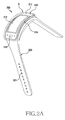
- an electronic device 200 is a wrist-mounted wearable electronic device that can be worn on a user's wrist.
- the electronic device 200 may include a main body 210 and a connection part 220 (e.g., a strap) on which the main body 210 is mounted.
- the electronic device 200 may be worn by winding the connection part 220 around the user's wrist while the main body 210 is placed on the wrist, and the connection part 220 may include a plurality of openings 221 formed at a certain interval such that the wearing position of the electronic device 200 may be adjusted to be suitable for the user's wrist.
- the connection part 220 may be formed of at least one of metal, leather, rubber, silicon, and urethane.
- the main body 210 may include a display 212 on a front side 211 thereof.
- a touch screen type of display 212 may be employed.
- at least one key button 213 may be disposed in a proper place of the main body 210.
- the electronic device 200 may have a battery (e.g., a rechargeable battery, and the like) therein as a power supply means, and may be selectively mountable on a portable charging cradle in order to charge the battery.
- a battery e.g., a rechargeable battery, and the like
- the electronic device 200 may include a plurality of terminals 216 on a rear side 215 of the main body 210 thereof, which may be electrically and physically connectable to connector pins of the cradle described above.
- the terminals 216 may be exposed through the rear side 215 of the main body 210, and may be disposed to be flush with or lower than the rear side 215.
- the electronic device 200 may also further include a sensor 217 on the rear side 215 of the main body 210 thereof, which measures the heart rate for the user's health care when the electronic device 200 is worn on the user's wrist.
- a speaker hole 218 for releasing a speaker sound, which is output through a speaker embedded in the electronic device, to the outside may be disposed on the rear side 215 of the main body 210.
- a microphone hole for receiving the user's voice may also be formed in a proper place of the electronic device 200 to correspond to a microphone that is disposed in the interior of the electronic device 200.
- the electronic device 200 may be subordinated to another electronic device, and may be used together therewith through a certain communication method. According to an embodiment of the present disclosure, the electronic device 200 may also perform wireless communication with the other electronic device using a short-range communication module, such as Bluetooth, BT, and the like. However, the present disclosure is not limited thereto, and the electronic device 200 may also include a communication module and an antenna device so as to be independently used as an electronic device for communication.
- a short-range communication module such as Bluetooth, BT, and the like.
- the present disclosure is not limited thereto, and the electronic device 200 may also include a communication module and an antenna device so as to be independently used as an electronic device for communication.
- the electronic device 200 may include a metal bezel 214 that serves as the external appearance of the main body 210 and is used as decoration member.
- the metal bezel 214 may be formed in the form of a loop that surrounds the periphery of the display 212, and may be disposed in such a manner that at least a part thereof is exposed to the outside of the main body 210.
- the metal bezel 214 may serve as an antenna radiator of the electronic device 200.
- area A of FIG. 2A may be an area where the metal bezel 214 is disposed as an antenna radiator.
- the metal bezel 214 may serve as a multi-band antenna radiator that operates in two or more bands.
- the metal bezel 214 in the form of a loop which serves as the external appearance of the electronic device 200 and is used as a decoration member, may be used as an antenna radiator such as to exclude a separate antenna radiator mounting space that would otherwise have to be provided in the interior of the electronic device 200 for mounting such a separate antenna.
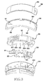
- FIG. 3 is an exploded perspective view of an electronic device according to various embodiments of the present disclosure.
- an electronic device 300 may be the same device as the electronic device 200 of FIGS. 2A and 2B .
- the electronic device 300 may include the connection part.
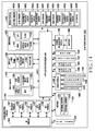
- the electronic device 300 may include an outer housing 310 that has a component mounting space 3101 therein, and a substrate 320, an inner housing 330, a metal bezel 340, and a display 350 which are sequentially mounted in the component mounting space 3101 of the outer housing 310.
- the metal bezel 340 may be formed in the shape of a loop that has a space 3401 in the center thereof. According to an embodiment of the present disclosure, although the metal bezel 340 is implemented in the shape of a closed loop, the metal bezel 340 may also have the shape of a partially open loop that includes a cutaway portion in at least one location. According to an embodiment of the present disclosure, the metal bezel 340 may include a power supply part 341 that may be electrically connected to a substrate power-supply part 321 of the substrate 320. According to an embodiment of the present disclosure, the metal bezel 340 may include a first ground part 342 that may be electrically connected to a first substrate ground part 322 of the substrate 320.
- the metal bezel 340 may include a second ground part 343 that may be electrically connected to a second substrate ground part 323 of the substrate 320.
- the first and second ground parts 342 and 343 may be disposed in the metal bezel 340 such that the distance from the power supply part 341 to the first ground part 342 differs from that from the power supply part 341 to the second ground part 343. This is for implementing an antenna radiator that can operate in different bands by making the electrical lengths from the power supply part 341 to the respective ground parts 342 and 343 different from each other.
- the inner housing 330 may be interposed between the metal bezel 340 and the substrate 320.
- the inner housing 330 may include an upper surface 331 and side surfaces 332 that are bent along at least part of the periphery of the upper surface 331.
- the side surfaces 332 include a plurality of conductive patterns (R1 and R2 of FIG. 6 and R3 and R4 of FIG.
- the patterns may be disposed such that the power supply part 341 and the first and second ground parts 342 and 343 of the metal bezel 340 are electrically connected to the substrate power-supply part 321 and the first and second substrate ground parts 322 and 323 of the substrate 320, respectively, by opposite ends thereof.
- the inner housing 330 which includes the conductive patterns, is interposed between the metal bezel 340 and the substrate 320, a change may be easily made to a desired frequency band by adjusting the electrical lengths of the conductive patterns in cases where the distance between the metal bezel 340 and the substrate 320 is relatively increased, or it is difficult to realize an operation only with the metal bezel 340 in the desired frequency band.
- the configuration of such conductive patterns will be described below.
- a first bezel connection part 3321 that is electrically connected to the first ground part 342 of the metal bezel 340 may be formed on the side surface 332 of the inner housing 330.
- a second bezel connection part 3322 that is electrically connected to the second ground part 343 of the metal bezel 343 may be formed on the side surface 332 of the inner housing 330.
- a first substrate connection part 3323 that is electrically connected to the first substrate ground part 322 of the substrate 320 may be formed on the side surface 332 of the inner housing 330.
- a second substrate connection part 3324 that is electrically connected to the second substrate ground part 323 of the substrate 320 may be formed on the side surface 332 of the inner housing 330. According to an embodiment of the present disclosure, only by an operation of installing the metal bezel 340, the inner housing 330, and the substrate 320, the bezel 340 may be electrically connected to the substrate 320 through the above-described connection parts 3321, 3322, 3323, and 3324 of the inner housing 330.
- the power supply part 341 of the metal bezel 340 may be directly brought into physical and electrical contact with the substrate power-supply part 321 of the substrate 320.
- the present disclosure is not limited thereto, and the metal bezel 340 and the substrate 320 may also be electrically and physically connected to each other by using the conductive patterns of the inner housing 330.
- the first and second ground parts 342 and 343 of the metal bezel 340 may be directly physically and electrically connected to the substrate ground parts 322 and 323 of the substrate 320 without using the conductive patterns of the inner housing 330.
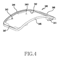
- FIG. 4 is a perspective view of a metal bezel, which is utilized as an antenna radiator, according to various embodiments of the present disclosure.
- the metal bezel 340 may be formed in the shape of a loop that has the space 3401 in the center thereof. According to an embodiment of the present disclosure, the metal bezel 340 may be applied in such a manner that the display 350 of the electronic device 300 is disposed in the central space 3401. However, the present disclosure is not limited thereto, and the metal bezel 340 may also serve as a decoration member in various areas of the electronic device 300. According to an embodiment of the present disclosure, at least part of the metal bezel 340 may also be exposed to the outside of the electronic device 300. According to an embodiment of the present disclosure, the metal bezel 340 may also be formed in the shape of a partially open loop rather than a closed loop. In this case, the metal bezel 340 may also be formed in such a manner that an opened cutaway portion is filled with a dielectric material.
- the metal bezel 340 may include a left bezel part 344, a right bezel part 345, an upper bezel part 346, and a lower bezel part 347.
- the metal bezel 340 may include the power supply part 341 extending downwards from the right side of the upper bezel part 346.
- the power supply part 341 may have enough length to make direct physical contact with the substrate 320.
- the first and second ground parts 342 and 343 may be sequentially formed with a certain interval therebetween on the left bezel part 344.
- the first and second ground parts 342 and 343 may be formed to physically contact the first and second bezel connection parts 3321 and 3322 of the inner housing 330.
- the first and second ground parts 342 and 343 may be disposed in the metal bezel 340 such that the distance from the power supply part 341 to the first ground part 342 differs from that from the power supply part 341 to the second ground part 343.
- the distance from the power supply part 341 to the first ground part 342 in one direction may be different from the distance from the power supply part 341 to the second ground part 343 in the opposite direction.
- the part of the metal bezel 340 formed from the power supply part 341 to the first ground part 342 may be used as an antenna radiator that operates in a higher frequency band than the part of the metal bezel 340 formed from the power supply part 341 to the second ground part 343.
- the whole part of the metal bezel 340 may also be used as a planar inverted-f antenna (PIFA) that operates in a relatively higher frequency band.
- PIFA planar inverted-f antenna
- FIG. 5 illustrates a state in which an inner housing and a substrate are applied to a metal bezel according to various embodiments of the present disclosure.
- the first ground part 342 of the metal bezel 340 may be electrically connected to the first bezel connection part 3321 formed on the side surface 332 of the inner housing 330 while the metal bezel 340 and the inner housing 330 are coupled to each other.
- the second ground part 343 of the metal bezel 340 may be electrically connected to the second bezel connection part 3322 formed on the side surface 332 of the inner housing 330.
- the first substrate ground part 322 of the substrate 320 may be electrically connected to the first substrate connection part 3323 of the inner housing 330, and the second substrate ground part 323 of the substrate 320 may be electrically connected to the second substrate connection part 3324 of the inner housing 330.
- one or more conductive patterns (R1, R2, R3, and R4 of FIGS. 5 and 6 ), which have a certain length and shape, may be formed on the side surface 332 of the inner housing 330.
- at least one pattern may electrically connect the first bezel connection part 3321 and the first substrate connection part 3323.
- at least one pattern may electrically connect the second bezel connection part 3322 and the second substrate connection part 3324.
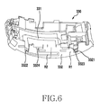
- FIGS. 6 and 7 are perspective views of an inner housing according to various embodiments of the present disclosure.
- the inner housing 330 may include a pair of conductive patterns R1 and R2 formed on the side surface 332 thereof.
- the conductive pattern R1 may operate together with an antenna radiator in the shape of a loop in a relatively higher frequency band that is formed by the power supply part 341 and the first ground part 342 of the metal bezel 340, and the substrate 320.
- the conductive pattern R2 may operate together with an antenna radiator in the shape of a loop in a relatively lower frequency band that is formed by the power supply part 341 and the second ground part 343 of the metal bezel 340, and the substrate 320.
- the first bezel connection part 3321 may be electrically connected to the first ground part 342 of the metal bezel 340, and the first substrate connection part 3323 may be electrically connected to the first substrate ground part 332 of the substrate 320.
- the conductive pattern R1 functions to electrically connect the first ground part 342 of the metal bezel 340 to the first substrate ground part 322 of the substrate 320.
- the second bezel connection part 3322 may be electrically connected to the second ground part 343 of the metal bezel 340, and the second substrate connection part 3324 may be electrically connected to the second substrate ground part 323 of the substrate 320.
- the conductive pattern R2 functions to electrically connect the second ground part 343 of the metal bezel 340 to the second substrate ground part 323 of the substrate 320.
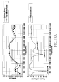
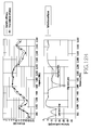
- FIG. 12A is a graph depicting a characteristic of an antenna device when an inner housing is applied according to various embodiments of the present disclosure.
- a graph is illustrated depicting the radiation characteristic of the metal bezel 340, which is used as an antenna radiator, when the conductive patterns R1 and R2 of FIG. 6 are applied, and each resonance mode can be identified from the reflection coefficient characteristic.
- the inner housing 330 may include a pair of conductive patterns R3 and R4 formed on the side surface 332 thereof.
- the conductive pattern R3 may operate together with an antenna radiator in the shape of a loop in a relatively higher frequency band that is formed by the power supply part 341 and the first ground part 342 of the metal bezel 340, and the substrate 320.
- the conductive pattern R4 may operate together with an antenna radiator in the shape of a loop in a relatively lower frequency band that is formed by the power supply part 341 and the second ground part 343 of the metal bezel 340, and the substrate 320.
- the first bezel connection part 3321 may be electrically connected to the first ground part 342 of the metal bezel 340, and the first substrate connection part 3323 may be electrically connected to the first substrate ground part 322 of the substrate 320.
- the conductive pattern R3 functions to electrically connect the first ground part 342 of the metal bezel 340 to the first substrate ground part 322 of the substrate 320.
- the second bezel connection part 3322 may be electrically connected to the second ground part 343 of the metal bezel 340, and the second substrate connection part 3324 may be electrically connected to the second substrate ground part 323 of the substrate 320.
- the conductive pattern R4 functions to electrically connect the second ground part 343 of the metal bezel 340 to the second substrate ground part 323 of the substrate 320.
- FIG. 12B is a graph depicting a characteristic of an antenna device when an inner housing is applied according to various embodiments of the present disclosure.
- a graph is illustrated depicting the radiation characteristic of the metal bezel 340, which is used as an antenna radiator, when the conductive patterns R3 and R4 of FIG. 7 are applied, and each resonance mode can be identified from the reflection coefficient characteristic.
- the resonant frequency in the low frequency band is lowered when the electrical length of the conductive pattern R2 in the low frequency band is formed to be longer than that of the conductive pattern R4 in the metal bezel 340 which has the same shape and condition.
- the conductive patterns R1, R2, R3, and R4 may be formed on the inner housing 330, which is made of a synthetic resin material, through a laser direct structuring (LDS) method.
- LDS laser direct structuring
- the conductive patterns may also be formed through in-mold antenna (IMA) method, or if there is space, the conductive patterns may also be formed in such a manner that at least one of a flexible printed circuit (FPC) on which a thin metal plate or pattern is formed and a metal tape is attached to the side surface of the inner housing.
- the conductive patterns may also be formed in such a manner of applying a conductive spray to the side surface of the inner housing.
- the conductive patterns may also be formed by insert molding or double injection molding in such a manner that the conductive patterns are or are not exposed through the inner or outer surface of the inner housing, which is made of a synthetic resin material.
- the two conductive patterns R1 and R2 or R3 and R4 disposed on the side surface 332 of the inner housing 330 only one may be electrically connected to the substrate ground parts 322 and 323 of the substrate 320, and the other may not be connected thereto and may be used as a parasitic pattern, thereby ensuring a broadband antenna performance and forming different frequency performances according to length and width variations.
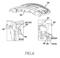
- FIG. 8 illustrates a state in which a metal bezel and a substrate are electrically connected by an inner housing according to various embodiments of the present disclosure.
- the first and second bezel connection parts 3321 and 3322 of the inner housing 330 may be brought into physical contact with each other by the first and second ground parts 342 and 343 of the metal bezel 340 and a conductive connection member 360.
- the first and second substrate connections parts 3323 and 3324 of the inner housing 330 may also be brought into physical contact with each other by the first and second substrate ground parts 322 and 323 of the substrate 320 and the conductive connection member 360.
- a conductive sponge or a conductive Poron tape may be used as the conductive connection member 360.
- the power supply part of the metal bezel 340 and the substrate power-supply part of the substrate 320 may also be brought into direct contact with each other, may be electrically connected to each other using the above-described conductive connection part 360, or may be connected to each other using a connecting member, such as a C-clip, and the like.
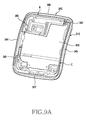
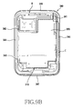
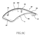
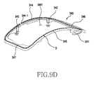
- FIGS. 9A , 9B , 9C , and 9D schematically illustrate electrical lengths in various frequency bands that are applied when a metal bezel is used as an antenna radiator according to various embodiments of the present disclosure.
- a radiation area B in a relatively higher frequency band may be formed by an antenna in the shape of a loop which is formed by the power supply part 341 and the first ground part 342 of the metal bezel 340 and the substrate 320.
- the dotted closed curve C may correspond to the loop, and the length of the loop may form a lambda length.
- PCB printed circuit board
- At least one of the power supply part 341 and the first and second ground parts 342 and 343 of the metal bezel 340 may be used as a ground part so that the whole metal bezel may also form the operating area D of the PIFA.
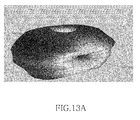
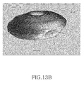
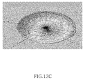
- FIGS. 13A , 13B , and 13C illustrate radiation patterns of a metal bezel, which is used as an antenna radiator, in various frequency bands according to various embodiments of the present disclosure.
- FIG. 13A illustrates the radiation pattern of an antenna in the shape of a loop in a high frequency band, and it can be seen that there is Null in the Y-axis direction because the metal bezel operates as an antenna in the shape of a loop.
- FIG. 13B illustrates the radiation pattern of a PIFA in a high frequency band.
- FIG. 13C illustrates the radiation pattern of an antenna in the shape of a loop in a low frequency band. It can be seen that there is Null in the Z-axis direction because the metal bezel operates as a loop antenna.
- a high frequency band may be expanded by adjusting the frequency bands of an antenna in the shape of a loop and a PIFA in the high frequency band.
- operating frequency bands of a high frequency band and a low frequency band may be adjusted by changing the location of each ground part, an undesired mechanical change according to antenna design may be minimized when the metal bezel is used as a decoration member or external appearance of an electronic device.
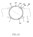
- FIG. 10 illustrates an electronic device to which a circular metal bezel is applied according to various embodiments of the present disclosure.
- a circular metal bezel 1011 which is applied to a circular electronic device 1000 rather than a rectangular electronic device, may also be used as the same loop type of antenna radiator as described above.
- the electronic device 1000 may include a main body 1010 that is fixed by a connection part 1020, and the metal bezel 1011 may be installed in such a manner of surrounding a circular display 1012.
- the metal bezel 1011 may have the shape of a closed loop, or may have the shape of a partially open loop that includes at least one cutaway portion 344-1 as illustrated in FIG. 9D .
- the metal bezel 1011 may include a power supply part 1013 and first and second ground parts 1014 and 1015 that are spaced a certain distance apart from the power supply part 1013, and the power supply part 1013 and the first and second ground parts 1014 and 1015 may be electrically connected to a substrate in the interior of a main body, which is not illustrated.
- the metal bezel 1011 may be used as a multi-band antenna device operating in different frequency bands, for example, by a radiation area E from the power supply part 1013 to the first ground part 1014 in one direction and another radiation area F from the power supply part 1013 to the second ground part 1015 in another direction.
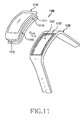
- FIG. 11 illustrates a state in which a metal bezel, as an antenna radiator, is applied to a connection part of a wearable electronic device according to various embodiments of the present disclosure.
- an electronic device 1100 may include a main body 1110 and a connection part 1120.
- the connection part 1120 may have a main-body insertion hole 1121 in which the main body 1110 is mounted.
- a metal bezel 1122 may be disposed along the inner periphery of the main-body insertion hole 1121.
- the main body 1110 may be formed in a positioning slit 1111 that may be seated on the main-body insertion hole 1121.
- a power supply part 1112 and first and second ground parts 1113 and 1114 which protrude toward the outside or are exposed to the outside, may be disposed on the positioning slit 1111.
- the power supply part 1112 and the first and second ground parts 1113 and 1114 are electrically connected to a substrate disposed in the interior of the main body 1110, and portions thereof protruding from the positioning slit may be implemented in the shape of a connector pin. According to an embodiment of the present disclosure, only by an operation of fixing the main body 1110 to the main-body insertion hole 1121 of the connection part 1120, the power supply part 1112 and the first and second ground parts 1113 and 1114, which are disposed in the positioning slit 1111 of the main body 1110, may be electrically connected to a preset area of the metal bezel 1122.
- the metal mechanical part can be used as an antenna radiator to achieve excellent radiation performance of the antenna device, and a separate mounting space for the antenna device can be excluded so that the metal mechanical part contributes to the slimness of the electronic device.
- FIG. 14 is a block diagram of a configuration of an electronic device according to an embodiment of the present disclosure.
- the electronic device 1401 may entirely or partially constitute the electronic device 101 of FIG. 1 , the device 200 of FIGS. 2A , 2B , and 3 .
- Electronic device 1401 includes at least one application processor (AP) 1410, a communication module 1420, a subscriber identification module (SIM) card 1424, a memory 1430, a sensor module 1440, an input device 1450, a display 1460, an interface 1470, an audio module 1480, a camera module 1490, a camera module 1491, a power management module 1495, a battery 1496, an indicator 1497, and a motor 1498.
- AP application processor
- SIM subscriber identification module
- the AP 1410 controls a plurality of hardware or software elements connected to the AP 1410 by driving an operating system or an application program.
- the AP 1410 processes a variety of data, including multimedia data, and performs arithmetic operations.
- the AP 1410 may be implemented, for example, with a system on chip (SoC).
- SoC system on chip
- the AP 1410 may further include a Graphical processing unit (GPU).
- GPU Graphical processing unit
- the communication module 1420 (e.g., the communication interface 160) performs data transmission/reception in communication between other electronic devices (e.g., the external electronic device 104 or the server 106) connected with the electronic device 1401 through a network.
- the communication module 1420 includes a cellular module 1421, a Wi-Fi module 1423, a BT module 1425, a GPS module 1427, a NFC module 1428, and a radio frequency (RF) module 1429.
- RF radio frequency
- the cellular module 1421 provides a voice call, a video call, a text service, an internet service, and the like, through a communication network (e.g., LTE, LTE-A, CDMA, WCDMA, UMTS, WiBro, and GSM, and the like).
- a communication network e.g., LTE, LTE-A, CDMA, WCDMA, UMTS, WiBro, and GSM, and the like.
- the cellular module 1421 identifies and authenticates the electronic device 1401 within the communication network by using a SIM card 1424.
- the cellular module 1421 may perform at least some of functions that can be provided by the AP 1410.
- the cellular module 1421 may perform at least some of multimedia control functions.
- the cellular module 1421 includes a communication processor (CP). Further, the cellular module 1421 may be implemented, for example, with an SoC. Although elements, such as the cellular module 1421 (e.g., the CP), the memory 1430, and the power management module 1495 are illustrated as separate elements with respect to the AP 1410 in FIG. 14 , the AP 1410 may also be implemented such that at least one part (e.g., the cellular module 1421) of the aforementioned elements is included in the AP 1410.
- the cellular module 1421 e.g., the CP
- the memory 1430 e.g., the memory 1430
- the power management module 1495 are illustrated as separate elements with respect to the AP 1410 in FIG. 14
- the AP 1410 may also be implemented such that at least one part (e.g., the cellular module 1421) of the aforementioned elements is included in the AP 1410.
- the AP 1410 or the cellular module 1421 (e.g., the CP) loads an instruction or data, which is received from each non-volatile memory connected thereto or at least one of different elements, to a volatile memory and processes the instruction or data.
- the AP 1410 or the cellular module 1421 stores data, which is received from at least one of different elements or generated by at least one of different elements, into the non-volatile memory.
- Each of the Wi-Fi module 1423, the BT module 1425, the GPS module 1427, and the NFC module 1428 includes a processor for processing data transmitted/received through a corresponding module.
- the cellular module 1421, the Wi-Fi module 1423, the BT module 1425, the GPS module 1427, and the NFC module 1428 are illustrated in FIG. 14 as separate blocks, according to one embodiment of the present disclosure, at least some (e.g., two or more) of the cellular module 1421, the Wi-Fi module 1423, the BT module 1425, the GPS module 1427, and the NFC module 1428 may be included in one integrated chip (IC) or IC package.
- IC integrated chip
- processors corresponding to the cellular module 1421, the Wi-Fi module 1423, the BT module 1425, the GPS module 1427, and the NFC module 1428 may be implemented with an SoC.
- the RF module 1429 transmits/receives data, for example an RF signal.
- the RF module 1429 may include, for example, a transceiver, a power amp module (PAM), a frequency filter, a low noise amplifier (LNA), and the like.
- the RF module 1429 may further include a component for transmitting/receiving a radio wave on a free space in wireless communication, for example, a conductor, a conducting wire, and the like. Although it is illustrated in FIG.
- the cellular module 1421, the Wi-Fi module 1423, the BT module 1425, the GPS module 1427, and the NFC module 1428 share one RF module 1429, according to one embodiment of the present disclosure, at least one of the cellular module 1421, the Wi-Fi module 1423, the BT module 1425, the GPS module 1427, the NFC module 1428 may transmit/receive an RF signal via a separate RF module.
- the SIM card 1424 is a card which is inserted into a slot formed at a specific location of the electronic device 1401.
- the SIM card 1424 includes unique identification information (e.g., an integrated circuit card identifier (ICCID)) or subscriber information (e.g., an international mobile subscriber identity (IMSI)).
- ICCID integrated circuit card identifier
- IMSI international mobile subscriber identity
- the memory 1430 (e.g., the memory 130) includes an internal memory 1432 or an external memory 1434.
- the internal memory 1432 may include, for example, at least one of a volatile memory (e.g., a dynamic random access memory (DRAM), a static RAM (SRAM), a synchronous dynamic RAM (SDRAM), and the like) or a non-volatile memory (e.g., a one time programmable read only memory (OTPROM), a programmable ROM (PROM), an erasable and programmable ROM (EPROM), an electrically erasable and programmable ROM (EEPROM), a mask ROM, a flash ROM, a not and (NAND) flash memory, a not or (NOR) flash memory, and the like).
- the internal memory 1432 may be a solid state drive (SSD).
- the external memory 1434 may include a flash drive, and may further include, for example, compact flash (CF), secure digital (SD), micro-SD, mini-SD, extreme digital (xD), memory stick, and the like.
- the external memory 1434 may be operatively coupled to the electronic device 1401 via various interfaces.
- the electronic device 1401 may further include a storage unit (or a storage medium), such as a hard drive.
- a storage unit or a storage medium
- a hard drive such as a hard drive
- the sensor module 1440 measures a physical quantity or detects an operation state of the electronic device 1401, and converts the measured or detected information into an electric signal.
- the sensor module 1440 includes, for example, at least one of a gesture sensor 1440A, a gyro sensor 1440B, a barometric pressure sensor 1440C, a magnetic sensor 1440D, an acceleration sensor 1440E, a grip sensor 1440F, a proximity sensor 1440G, a color sensor 1440H (e.g., a red, green, blue (RGB) sensor), a bio sensor 1440I, a temperature/humidity sensor 1440J, an illumination sensor 1440K, and an ultraviolet (UV) sensor 1440M.
- a gesture sensor 1440A e.g., a gyro sensor 1440B, a barometric pressure sensor 1440C, a magnetic sensor 1440D, an acceleration sensor 1440E, a grip sensor 1440F, a proximity sensor 1440G, a color sensor 1440H
- the sensor module 1440 may include, for example, an E-node sensor, an electromyography (EMG) sensor, an electroencephalogram (EEG) sensor, an electrocardiogram (ECG) sensor, a fingerprint sensor, and the like.
- the sensor module 1440 may further include a control circuit for controlling at least one or more sensors included therein.
- the input device 1450 includes a touch panel 1452, a (digital) pen sensor 1454, a key 1456, or an ultrasonic input unit 1458.
- the touch panel 1452 recognizes a touch input, for example, by using at least one of an electrostatic type, a pressure-sensitive type, and an ultrasonic type.
- the touch panel 1452 may further include a control circuit.
- the electrostatic type of touch panel 1452 not only is physical contact recognition possible, but proximity recognition is also possible.
- the touch penal 1452 may further include a tactile layer. In this case, the touch panel 1452 provides the user with a tactile reaction.
- the (digital) pen sensor 1454 may be implemented, for example, by using the same or similar method of receiving a touch input of the user or by using an additional sheet for recognition.
- the key 1456 may be, for example, a physical button, an optical key, a keypad, or a touch key.
- the ultrasonic input unit 1458 is a device by which the electronic device 1401 detects a sound wave through a microphone 1488 by using a pen which generates an ultrasonic signal, and is capable of radio recognition.
- the electronic device 1401 may use the communication module 1420 to receive a user input from an external device (e.g., a computer or a server) connected thereto.
- an external device e.g., a computer or a server
- the display 1460 (e.g., the display 150) includes a panel 1462, a hologram 1464, or a projector 1466.
- the panel 1462 may be, for example, a liquid-crystal display (LCD), an active-matrix organic light-emitting diode (AM-OLED), and the like.
- the panel 1462 may be implemented, for example, in a flexible, transparent, or wearable manner.
- the panel 1462 may be constructed as one module with the touch panel 1452.
- the hologram 1464 uses an interference of light and displays a stereoscopic image in the air.
- the projector 1466 displays an image by projecting a light beam onto a screen.
- the screen may be located inside or outside the electronic device 1401.
- the display 1460 may further include a control circuit for controlling the panel 1462, the hologram 1464, or the projector 1466.
- the interface 1470 includes, for example, an HDMI 1472, a USB 1474, an optical communication interface 1476, or a D-subminiature (D-sub) 1478.
- the interface 1470 may be included, for example, in the communication interface 160 of FIG. 1 .
- the interface 1470 may include, for example, mobile high-definition link (MHL) (not shown), SD/multi-media card (MMC) or infrared data association (IrDA).
- MHL mobile high-definition link
- MMC multi-media card
- IrDA infrared data association
- the audio module 1480 bilaterally converts a sound and electric signal. At least some elements of the audio module 1480 may be included in the input/output interface 140 of FIG. 1 .
- the audio module 1480 converts sound information which is input or output through a speaker 1482, a receiver 1484, an earphone 1486, the microphone 1488, and the like.
- Each of the camera modules 1490 and 1491 is a device for image and video capturing, and may include one or more image sensors (e.g., a front sensor or a rear sensor), a lens, an image signal processor (ISP) (not shown), or a flash (not shown, e.g., an LED or a xenon lamp).
- image sensors e.g., a front sensor or a rear sensor
- lens e.g., a lens
- ISP image signal processor
- flash not shown, e.g., an LED or a xenon lamp
- the power management module 1495 manages power of the electronic device 1401.
- the power management module 1495 may include a power management integrated circuit (PMIC), a charger IC, or a battery gauge.
- PMIC power management integrated circuit
- the PMIC may be placed inside an IC or SoC semiconductor. Charging is classified into wired charging and wireless charging.
- the charger IC charges a battery, and prevents an over-voltage or over-current flow from a charger.
- the charger IC includes a charger IC for at least one of the wired charging and the wireless charging.
- the wireless charging may be classified, for example, into a magnetic resonance type, a magnetic induction type, and an electromagnetic type.
- An additional circuit for the wireless charging for example, a coil loop, a resonant circuit, a rectifier, and the like, may be added.
- the battery gauge measures, for example, a residual quantity of the battery 1496 and a voltage, current, and temperature during charging.
- the battery 1496 stores or generates electricity and supplies power to the electronic device 1401 by using the stored or generated electricity.
- the battery 1496 may include a rechargeable battery or a solar battery.
- the indicator 1497 indicates a specific state, for example, a booting state, a message state, a charging state, and the like, of the electronic device 1401 or a part thereof (e.g., the AP 1410).
- the motor 1498 converts an electric signal into a mechanical vibration.
- the electronic device 1401 includes a processing unit (e.g., a GPU) for supporting mobile TV.
- the processing unit for supporting mobile TV processes media data according to a protocol of, for example, digital multimedia broadcasting (DMB), digital video broadcasting (DVB), media flow, and the like.
- DMB digital multimedia broadcasting
- DVD digital video broadcasting
- Each of the aforementioned elements of the electronic device may consist of one or more components, and names thereof may vary depending on a type of electronic device.
- the electronic device according to various embodiments of the present disclosure may include at least one of the aforementioned elements. Some of the elements may be omitted, or additional other elements may be further included. In addition, some of the elements of the electronic device may be combined and constructed as one entity, so as to equally perform functions of corresponding elements before combination.
- module used herein may imply a unit including one of hardware, software, and firmware, or a combination of them.
- the term “module” may be interchangeably used with terms, such as unit, logic, logical block, component, circuit, and the like.
- the “module” may be a minimum unit of an integrally constituted component or may be a part thereof.
- the “module” may be a minimum unit for performing one or more functions or may be a part thereof.
- the “module” may be mechanically or electrically implemented.
- the "module” of the present disclosure includes at least one of an application-specific IC (ASIC) chip, a field-programmable gate arrays (FPGAs), and a programmable-logic device, which are known or will be developed and which perform certain operations.
- ASIC application-specific IC
- FPGAs field-programmable gate arrays
- programmable-logic device which are known or will be developed and which perform certain operations.
- a device e.g., modules or functions thereof
- method e.g., operations
- the instruction may be executed by one or more processors (e.g., the processor 1410), to perform a function corresponding to the instruction.
- the computer-readable storage media may be, for example, the memory 1430.
- At least some parts of the programming module may be implemented (e.g., executed), for example, by the processor 1410.
- At least some parts of the programming module may include modules, programs, routines, sets of instructions, processes, and the like, for performing one or more functions.
- a non-transitory computer readable recording medium is any data storage device that can store data which can be thereafter read by a computer system.
- Examples of the non-transitory computer readable recording medium include a Read-Only Memory (ROM), a Random-Access Memory (RAM), Compact Disc-ROMs (CD-ROMs), magnetic tapes, floppy disks, and optical data storage devices.
- the non-transitory computer readable recording medium can also be distributed over network coupled computer systems so that the computer readable code is stored and executed in a distributed fashion.
- functional programs, code, and code segments for accomplishing the present disclosure can be easily construed by programmers skilled in the art to which the present disclosure pertains.
- the various embodiments of the present disclosure as described above typically involve the processing of input data and the generation of output data to some extent.
- This input data processing and output data generation may be implemented in hardware or software in combination with hardware.
- specific electronic components may be employed in a mobile device or similar or related circuitry for implementing the functions associated with the various embodiments of the present disclosure as described above.
- one or more processors operating in accordance with stored instructions may implement the functions associated with the various embodiments of the present disclosure as described above. If such is the case, it is within the scope of the present disclosure that such instructions may be stored on one or more non-transitory processor readable mediums.
- processor readable mediums examples include a ROM, a RAM, CD-ROMs, magnetic tapes, floppy disks, and optical data storage devices.
- the processor readable mediums can also be distributed over network coupled computer systems so that the instructions are stored and executed in a distributed fashion.
- functional computer programs, instructions, and instruction segments for accomplishing the present disclosure can be easily construed by programmers skilled in the art to which the present disclosure pertains.
- the module or programming module may further include at least one or more elements among the aforementioned elements, may omit some of them, or may further include additional elements.
- Operations performed by a module, programming module, or other elements may be executed in a sequential, parallel, repetitive, or heuristic manner. In addition, some of the operations may be executed in a different order or may be omitted, or other operations may be added.
Landscapes
- Physics & Mathematics (AREA)
- General Physics & Mathematics (AREA)
- Engineering & Computer Science (AREA)
- Computer Networks & Wireless Communication (AREA)
- Optics & Photonics (AREA)
- Signal Processing (AREA)
- Support Of Aerials (AREA)
- Telephone Set Structure (AREA)
Applications Claiming Priority (1)
| Application Number | Priority Date | Filing Date | Title |
|---|---|---|---|
| KR1020140115713A KR102177285B1 (ko) | 2014-09-01 | 2014-09-01 | 안테나 장치 및 그것을 포함하는 전자 장치 |
Publications (3)
| Publication Number | Publication Date |
|---|---|
| EP2990889A2 true EP2990889A2 (de) | 2016-03-02 |
| EP2990889A3 EP2990889A3 (de) | 2016-11-23 |
| EP2990889B1 EP2990889B1 (de) | 2020-08-19 |
Family
ID=54014729
Family Applications (1)
| Application Number | Title | Priority Date | Filing Date |
|---|---|---|---|
| EP15183356.3A Active EP2990889B1 (de) | 2014-09-01 | 2015-09-01 | Antennenvorrichtung und elektronische vorrichtung, die eine solche antenne umfasst |
Country Status (5)
| Country | Link |
|---|---|
| US (1) | US10297909B2 (de) |
| EP (1) | EP2990889B1 (de) |
| KR (1) | KR102177285B1 (de) |
| CN (1) | CN106662844B (de) |
| WO (1) | WO2016036099A1 (de) |
Cited By (3)
| Publication number | Priority date | Publication date | Assignee | Title |
|---|---|---|---|---|
| EP3291369A1 (de) * | 2016-09-05 | 2018-03-07 | Samsung Electronics Co., Ltd. | Elektronische vorrichtung mit mehrbandantenne |
| CN107959116A (zh) * | 2016-10-14 | 2018-04-24 | 天迈科技股份有限公司 | 具导电胶天线的壳体及其导电胶天线结构 |
| CN109301479A (zh) * | 2018-10-31 | 2019-02-01 | 广东小天才科技有限公司 | 具有天线结构的智能穿戴设备 |
Families Citing this family (43)
| Publication number | Priority date | Publication date | Assignee | Title |
|---|---|---|---|---|
| US10108900B2 (en) | 2014-10-18 | 2018-10-23 | Chi Huynh | Jewelry with security bezel for regulating near field communication with an embedded near field communication chip |
| US9824310B2 (en) | 2015-01-05 | 2017-11-21 | Chi Huynh | Article of jewelry with hidden near field communication (NFC) chip and metallic bezel substantially surrounding the NFC chip and uses thereof |
| DE102015115574A1 (de) * | 2014-11-13 | 2016-05-19 | Samsung Electronics Co., Ltd. | Nahfeldkommunikations-Chip, der in eine tragbare elektronische Vorrichtung eingebettet ist, und tragbare elektronische Vorrichtung |
| US10257680B2 (en) | 2014-12-02 | 2019-04-09 | Bruce Quarto | Methods and systems for purchasing, sharing and transferring ownership of digital music using authenticated data files from near field communication (NFC) chips |
| US10333200B2 (en) * | 2015-02-17 | 2019-06-25 | Samsung Electronics Co., Ltd. | Portable device and near field communication chip |
| KR102429811B1 (ko) | 2015-08-13 | 2022-08-08 | 삼성전자주식회사 | 다중 대역 안테나를 포함하는 전자 장치 |
| KR102150695B1 (ko) | 2015-08-13 | 2020-09-01 | 삼성전자주식회사 | 다중 대역 안테나를 포함하는 전자 장치 |
| US10374662B2 (en) * | 2015-09-04 | 2019-08-06 | Lg Electronics Inc. | Watch-type mobile terminal |
| US20170194709A1 (en) * | 2015-12-31 | 2017-07-06 | Aac Acoustic Technologies (Shenzhen) Co., Ltd. | Multi-Structure Metal Antenna |
| EP3442373A4 (de) * | 2016-04-12 | 2020-04-08 | Chi Huynh | Schmuck mit sicherheitslünette zur regelung der nahfeldkommunikation mit einem eingebetteten nahfeldkommunikationschip |
| US10615489B2 (en) * | 2016-06-08 | 2020-04-07 | Futurewei Technologies, Inc. | Wearable article apparatus and method with multiple antennas |
| CN107546462A (zh) * | 2016-06-23 | 2018-01-05 | 华为终端(东莞)有限公司 | 一种智能可穿戴产品的近场通信天线及智能可穿戴产品 |
| US10431878B2 (en) * | 2016-06-23 | 2019-10-01 | Verizon Patent And Licensing Inc. | Wearable device design for 4G antennas |
| TWI629832B (zh) * | 2016-06-30 | 2018-07-11 | 和碩聯合科技股份有限公司 | 穿戴型電子裝置 |
| KR102584972B1 (ko) * | 2016-08-29 | 2023-10-05 | 삼성전자주식회사 | 다중 대역 안테나를 포함하는 웨어러블 전자 장치 |
| TWI633706B (zh) * | 2016-09-01 | 2018-08-21 | 和碩聯合科技股份有限公司 | 穿戴式電子裝置 |
| KR102591805B1 (ko) * | 2016-11-04 | 2023-10-23 | 삼성전자주식회사 | 웨어러블 전자 장치의 안테나 |
| CN106450684B (zh) * | 2016-12-27 | 2023-12-05 | 深圳市中天迅通信技术股份有限公司 | 一种结合金属外壳的近场天线装置 |
| KR102612537B1 (ko) * | 2016-12-30 | 2023-12-11 | 삼성전자 주식회사 | 안테나용 빔 형성 보조부 및 이를 포함하는 단말 |
| US10879596B2 (en) * | 2017-01-31 | 2020-12-29 | Intel Corporation | Antenna for wearable devices methods, apparatuses, and systems |
| KR102307730B1 (ko) | 2017-04-10 | 2021-10-05 | 삼성전자주식회사 | 전자 장치의 하우징에 포함된 도전성 물질을 이용하는 안테나를 포함하는 전자 장치 |
| KR102392724B1 (ko) * | 2017-08-30 | 2022-04-29 | 삼성전자주식회사 | 웨어러블 전자 장치의 안테나 |
| CN107861375A (zh) * | 2017-10-23 | 2018-03-30 | 惠州Tcl移动通信有限公司 | 一种具有二合一天线的智能手表 |
| JP7336946B2 (ja) * | 2017-11-02 | 2023-09-01 | カシオ計算機株式会社 | アンテナ装置および時計 |
| JP2019086414A (ja) | 2017-11-07 | 2019-06-06 | カシオ計算機株式会社 | 電子時計 |
| KR102500480B1 (ko) * | 2017-12-22 | 2023-02-16 | 삼성전자주식회사 | 접촉 부재를 포함하는 전자 장치 및 그 제작 방법 |
| CN108109827A (zh) * | 2018-01-11 | 2018-06-01 | 信利光电股份有限公司 | 一种背面盖板的制作方法和背面盖板 |
| CN108598666B (zh) * | 2018-05-28 | 2020-11-13 | 北京小米移动软件有限公司 | 终端壳体及终端 |
| US10734714B2 (en) * | 2018-05-29 | 2020-08-04 | Apple Inc. | Electronic device wide band antennas |
| KR102018777B1 (ko) * | 2018-08-14 | 2019-09-06 | 주식회사 센서뷰 | 다중 대역 안테나를 갖는 웨어러블 기기 |
| TWI676870B (zh) * | 2018-10-19 | 2019-11-11 | 巨擘科技股份有限公司 | 腕錶及其省電方法 |
| US10509994B1 (en) | 2019-05-08 | 2019-12-17 | Chi Huynh | Ring for use in near field communication (NFC) and method of making same |
| KR102293939B1 (ko) * | 2019-09-05 | 2021-08-26 | (주)파트론 | 3d 프린팅 방식에 의해 형성되는 안테나부를 포함하는 웨어러블 전자장치 |
| CN111082204B (zh) * | 2019-11-28 | 2022-01-25 | 歌尔股份有限公司 | 智能手环 |
| CN113690582B (zh) * | 2020-05-19 | 2023-02-03 | 华为技术有限公司 | 一种可穿戴设备 |
| ES3048609T3 (en) * | 2020-06-05 | 2025-12-11 | Anhui Huami Health Tech Co Ltd | Wearable device |
| US12174660B2 (en) | 2020-06-11 | 2024-12-24 | Apple Inc. | Electronic device |
| US11573599B2 (en) | 2020-06-11 | 2023-02-07 | Apple Inc. | Electrical connectors for electronic devices |
| US11880237B1 (en) * | 2020-09-25 | 2024-01-23 | Amazon Technologies, Inc. | Wearable device with display |
| US11534086B2 (en) | 2020-10-30 | 2022-12-27 | Medtronic Minimed, Inc. | Low-profile wearable medical device |
| JP7127708B2 (ja) * | 2021-03-03 | 2022-08-30 | カシオ計算機株式会社 | ウェアラブル機器 |
| CN117941176A (zh) | 2021-09-07 | 2024-04-26 | 三星电子株式会社 | 天线和包括该天线的电子装置 |
| CN119768744A (zh) * | 2022-07-28 | 2025-04-04 | 三星电子株式会社 | 包括电路板的阻尼结构的可穿戴电子装置 |
Family Cites Families (27)
| Publication number | Priority date | Publication date | Assignee | Title |
|---|---|---|---|---|
| EP0741434B1 (de) | 1995-05-05 | 2001-03-14 | Eta SA Fabriques d'Ebauches | Antennenstruktur für eine Uhr |
| US5736965A (en) * | 1996-02-07 | 1998-04-07 | Lutron Electronics Co. Inc. | Compact radio frequency transmitting and receiving antenna and control device employing same |
| DE69906973T2 (de) | 1999-10-11 | 2004-02-26 | Asulab S.A. | Antennenstruktur die ein Gehäuse bildet für elektronische Komponente eines tragbaren Gerätes |
| US6762728B2 (en) | 2000-03-29 | 2004-07-13 | Seiko Epson Corporation | Antenna device for high-frequency radio apparatus and wrist watch-type radio apparatus |
| KR100678232B1 (ko) | 2000-12-30 | 2007-02-01 | 삼성전자주식회사 | 폴더타입 휴대용 무선단말기의 내장형 안테나 장치 |
| JP3689382B2 (ja) | 2001-05-01 | 2005-08-31 | Tdk株式会社 | 無線通信カード |
| CN1241442C (zh) * | 2001-12-14 | 2006-02-08 | 广达电脑股份有限公司 | 手机内藏式天线模块 |
| EP1378805B1 (de) | 2002-07-02 | 2007-01-17 | CSEM Centre Suisse d'Electronique et de Microtechnique SA Recherche et Développement | Uhrwerk mit Antenne |
| EP1445821A1 (de) | 2003-02-06 | 2004-08-11 | Matsushita Electric Industrial Co., Ltd. | Tragbares Funkkommunikationsgerät mit einem Auslegerteil |
| US7202790B2 (en) * | 2004-08-13 | 2007-04-10 | Sensormatic Electronics Corporation | Techniques for tuning an antenna to different operating frequencies |
| US7612725B2 (en) | 2007-06-21 | 2009-11-03 | Apple Inc. | Antennas for handheld electronic devices with conductive bezels |
| JP5029201B2 (ja) | 2007-08-08 | 2012-09-19 | セイコーエプソン株式会社 | 受信装置、電波時計および受信方法 |
| JP5145896B2 (ja) | 2007-11-21 | 2013-02-20 | 富士通株式会社 | 電子装置および電子装置製造方法 |
| KR101529921B1 (ko) | 2008-11-04 | 2015-06-18 | 엘지전자 주식회사 | 와치형 단말기 |
| KR101622606B1 (ko) * | 2009-07-15 | 2016-05-20 | 엘지전자 주식회사 | 와치형 휴대 단말기 |
| CN102760940B (zh) | 2011-04-29 | 2015-05-27 | 纬创资通股份有限公司 | 耦合式天线及具有耦合式天线的电子装置 |
| TW201304272A (zh) | 2011-07-15 | 2013-01-16 | Wistron Neweb Corp | 隨身電子裝置之天線結構及隨身無線電子裝置 |
| US8698680B2 (en) | 2012-01-17 | 2014-04-15 | Garmin Switzerland Gmbh | Watch with improved ground plane |
| US9172148B2 (en) * | 2013-02-08 | 2015-10-27 | Garmin Switzerland Gmbh | Watch with bezel antenna configuration |
| US10594025B2 (en) * | 2013-03-11 | 2020-03-17 | Suunto Oy | Coupled antenna structure and methods |
| US9196952B2 (en) * | 2013-03-15 | 2015-11-24 | Qualcomm Incorporated | Multipurpose antenna |
| CN203481374U (zh) | 2013-07-11 | 2014-03-12 | 中兴通讯股份有限公司 | 终端 |
| US9444141B2 (en) * | 2013-08-19 | 2016-09-13 | Google Technology Holdings LLC | Antenna system for a smart portable device using a continuous metal band |
| CN203747019U (zh) | 2014-02-24 | 2014-07-30 | 联想(北京)有限公司 | 电子设备 |
| KR20160052253A (ko) * | 2014-11-04 | 2016-05-12 | 삼성전자주식회사 | 안테나 장치 및 그것을 포함하는 전자 장치 |
| KR102348027B1 (ko) * | 2015-02-27 | 2022-01-07 | 삼성전자주식회사 | 접속 모듈 및 이를 포함하는 전자 장치 |
| US9985341B2 (en) * | 2015-08-31 | 2018-05-29 | Microsoft Technology Licensing, Llc | Device antenna for multiband communication |
-
2014
- 2014-09-01 KR KR1020140115713A patent/KR102177285B1/ko active Active
-
2015
- 2015-08-31 US US14/840,583 patent/US10297909B2/en active Active
- 2015-09-01 WO PCT/KR2015/009170 patent/WO2016036099A1/en not_active Ceased
- 2015-09-01 EP EP15183356.3A patent/EP2990889B1/de active Active
- 2015-09-01 CN CN201580044555.9A patent/CN106662844B/zh active Active
Non-Patent Citations (1)
| Title |
|---|
| None |
Cited By (7)
| Publication number | Priority date | Publication date | Assignee | Title |
|---|---|---|---|---|
| EP3291369A1 (de) * | 2016-09-05 | 2018-03-07 | Samsung Electronics Co., Ltd. | Elektronische vorrichtung mit mehrbandantenne |
| CN107799883A (zh) * | 2016-09-05 | 2018-03-13 | 三星电子株式会社 | 包括多频带天线的电子设备 |
| US10608323B2 (en) | 2016-09-05 | 2020-03-31 | Samsung Electronics Co., Ltd | Electronic device including multi-band antenna |
| CN107799883B (zh) * | 2016-09-05 | 2020-11-27 | 三星电子株式会社 | 包括多频带天线的电子设备 |
| CN107959116A (zh) * | 2016-10-14 | 2018-04-24 | 天迈科技股份有限公司 | 具导电胶天线的壳体及其导电胶天线结构 |
| CN109301479A (zh) * | 2018-10-31 | 2019-02-01 | 广东小天才科技有限公司 | 具有天线结构的智能穿戴设备 |
| CN109301479B (zh) * | 2018-10-31 | 2023-12-22 | 广东小天才科技有限公司 | 具有天线结构的智能穿戴设备 |
Also Published As
| Publication number | Publication date |
|---|---|
| US10297909B2 (en) | 2019-05-21 |
| EP2990889B1 (de) | 2020-08-19 |
| WO2016036099A1 (en) | 2016-03-10 |
| US20160064804A1 (en) | 2016-03-03 |
| CN106662844A (zh) | 2017-05-10 |
| CN106662844B (zh) | 2020-10-16 |
| KR20160026581A (ko) | 2016-03-09 |
| KR102177285B1 (ko) | 2020-11-10 |
| EP2990889A3 (de) | 2016-11-23 |
Similar Documents
| Publication | Publication Date | Title |
|---|---|---|
| EP2990889B1 (de) | Antennenvorrichtung und elektronische vorrichtung, die eine solche antenne umfasst | |
| US10594026B2 (en) | Antenna device and electronic device including the same | |
| CN108432043B (zh) | 天线以及包括其的电子装置 | |
| CN107408755B (zh) | 天线设备和具有该天线设备的电子设备 | |
| US9753501B2 (en) | Electrical connection device and electronic device having same | |
| CN107925152B (zh) | 包括多频带天线的电子设备 | |
| CN107210516B (zh) | 天线装置及包括天线装置的电子装置 | |
| EP3018540A1 (de) | Antennenvorrichtung und elektronische vorrichtung damit | |
| US9590291B2 (en) | Antenna apparatus and electronic device having the same | |
| EP2985983B1 (de) | Gehäuse, herstellungsverfahren dafür und elektronische vorrichtung mit dem gehäuse | |
| US10468750B2 (en) | Antenna and electronic device including the same | |
| US10461411B2 (en) | Antenna and electronic device including the same | |
| US10116039B2 (en) | Antenna apparatus and electronic device having the same | |
| US10547099B2 (en) | Antenna structure and electronic device including the same | |
| US10283846B2 (en) | Electronic device including metal housing antenna |
Legal Events
| Date | Code | Title | Description |
|---|---|---|---|
| PUAI | Public reference made under article 153(3) epc to a published international application that has entered the european phase |
Free format text: ORIGINAL CODE: 0009012 |
|
| AK | Designated contracting states |
Kind code of ref document: A2 Designated state(s): AL AT BE BG CH CY CZ DE DK EE ES FI FR GB GR HR HU IE IS IT LI LT LU LV MC MK MT NL NO PL PT RO RS SE SI SK SM TR |
|
| AX | Request for extension of the european patent |
Extension state: BA ME |
|
| RIC1 | Information provided on ipc code assigned before grant |
Ipc: G04G 21/04 20130101AFI20160530BHEP Ipc: G04R 60/06 20130101ALI20160530BHEP Ipc: H01Q 1/27 20060101ALI20160530BHEP |
|
| PUAL | Search report despatched |
Free format text: ORIGINAL CODE: 0009013 |
|
| AK | Designated contracting states |
Kind code of ref document: A3 Designated state(s): AL AT BE BG CH CY CZ DE DK EE ES FI FR GB GR HR HU IE IS IT LI LT LU LV MC MK MT NL NO PL PT RO RS SE SI SK SM TR |
|
| AX | Request for extension of the european patent |
Extension state: BA ME |
|
| RIC1 | Information provided on ipc code assigned before grant |
Ipc: G04R 60/06 20130101ALI20161014BHEP Ipc: G04G 21/04 20130101AFI20161014BHEP Ipc: H01Q 1/27 20060101ALI20161014BHEP |
|
| STAA | Information on the status of an ep patent application or granted ep patent |
Free format text: STATUS: REQUEST FOR EXAMINATION WAS MADE |
|
| 17P | Request for examination filed |
Effective date: 20170302 |
|
| RBV | Designated contracting states (corrected) |
Designated state(s): AL AT BE BG CH CY CZ DE DK EE ES FI FR GB GR HR HU IE IS IT LI LT LU LV MC MK MT NL NO PL PT RO RS SE SI SK SM TR |
|
| STAA | Information on the status of an ep patent application or granted ep patent |
Free format text: STATUS: EXAMINATION IS IN PROGRESS |
|
| 17Q | First examination report despatched |
Effective date: 20190605 |
|
| RIC1 | Information provided on ipc code assigned before grant |
Ipc: G04R 60/06 20130101ALI20200205BHEP Ipc: H01Q 1/27 20060101ALI20200205BHEP Ipc: H01Q 7/00 20060101ALI20200205BHEP Ipc: H01Q 15/00 20060101ALI20200205BHEP Ipc: H01Q 1/24 20060101ALI20200205BHEP Ipc: G04G 21/04 20130101AFI20200205BHEP Ipc: H01Q 5/371 20150101ALI20200205BHEP |
|
| GRAP | Despatch of communication of intention to grant a patent |
Free format text: ORIGINAL CODE: EPIDOSNIGR1 |
|
| STAA | Information on the status of an ep patent application or granted ep patent |
Free format text: STATUS: GRANT OF PATENT IS INTENDED |
|
| INTG | Intention to grant announced |
Effective date: 20200401 |
|
| GRAS | Grant fee paid |
Free format text: ORIGINAL CODE: EPIDOSNIGR3 |
|
| GRAA | (expected) grant |
Free format text: ORIGINAL CODE: 0009210 |
|
| STAA | Information on the status of an ep patent application or granted ep patent |
Free format text: STATUS: THE PATENT HAS BEEN GRANTED |
|
| AK | Designated contracting states |
Kind code of ref document: B1 Designated state(s): AL AT BE BG CH CY CZ DE DK EE ES FI FR GB GR HR HU IE IS IT LI LT LU LV MC MK MT NL NO PL PT RO RS SE SI SK SM TR |
|
| REG | Reference to a national code |
Ref country code: CH Ref legal event code: EP |
|
| REG | Reference to a national code |
Ref country code: DE Ref legal event code: R096 Ref document number: 602015057620 Country of ref document: DE |
|
| REG | Reference to a national code |
Ref country code: AT Ref legal event code: REF Ref document number: 1304650 Country of ref document: AT Kind code of ref document: T Effective date: 20200915 |
|
| REG | Reference to a national code |
Ref country code: IE Ref legal event code: FG4D |
|
| REG | Reference to a national code |
Ref country code: LT Ref legal event code: MG4D |
|
| REG | Reference to a national code |
Ref country code: NL Ref legal event code: MP Effective date: 20200819 |
|
| PG25 | Lapsed in a contracting state [announced via postgrant information from national office to epo] |
Ref country code: PT Free format text: LAPSE BECAUSE OF FAILURE TO SUBMIT A TRANSLATION OF THE DESCRIPTION OR TO PAY THE FEE WITHIN THE PRESCRIBED TIME-LIMIT Effective date: 20201221 Ref country code: LT Free format text: LAPSE BECAUSE OF FAILURE TO SUBMIT A TRANSLATION OF THE DESCRIPTION OR TO PAY THE FEE WITHIN THE PRESCRIBED TIME-LIMIT Effective date: 20200819 Ref country code: GR Free format text: LAPSE BECAUSE OF FAILURE TO SUBMIT A TRANSLATION OF THE DESCRIPTION OR TO PAY THE FEE WITHIN THE PRESCRIBED TIME-LIMIT Effective date: 20201120 Ref country code: FI Free format text: LAPSE BECAUSE OF FAILURE TO SUBMIT A TRANSLATION OF THE DESCRIPTION OR TO PAY THE FEE WITHIN THE PRESCRIBED TIME-LIMIT Effective date: 20200819 Ref country code: SE Free format text: LAPSE BECAUSE OF FAILURE TO SUBMIT A TRANSLATION OF THE DESCRIPTION OR TO PAY THE FEE WITHIN THE PRESCRIBED TIME-LIMIT Effective date: 20200819 Ref country code: HR Free format text: LAPSE BECAUSE OF FAILURE TO SUBMIT A TRANSLATION OF THE DESCRIPTION OR TO PAY THE FEE WITHIN THE PRESCRIBED TIME-LIMIT Effective date: 20200819 Ref country code: NO Free format text: LAPSE BECAUSE OF FAILURE TO SUBMIT A TRANSLATION OF THE DESCRIPTION OR TO PAY THE FEE WITHIN THE PRESCRIBED TIME-LIMIT Effective date: 20201119 Ref country code: BG Free format text: LAPSE BECAUSE OF FAILURE TO SUBMIT A TRANSLATION OF THE DESCRIPTION OR TO PAY THE FEE WITHIN THE PRESCRIBED TIME-LIMIT Effective date: 20201119 |
|
| REG | Reference to a national code |
Ref country code: AT Ref legal event code: MK05 Ref document number: 1304650 Country of ref document: AT Kind code of ref document: T Effective date: 20200819 |
|
| PG25 | Lapsed in a contracting state [announced via postgrant information from national office to epo] |
Ref country code: RS Free format text: LAPSE BECAUSE OF FAILURE TO SUBMIT A TRANSLATION OF THE DESCRIPTION OR TO PAY THE FEE WITHIN THE PRESCRIBED TIME-LIMIT Effective date: 20200819 Ref country code: NL Free format text: LAPSE BECAUSE OF FAILURE TO SUBMIT A TRANSLATION OF THE DESCRIPTION OR TO PAY THE FEE WITHIN THE PRESCRIBED TIME-LIMIT Effective date: 20200819 Ref country code: PL Free format text: LAPSE BECAUSE OF FAILURE TO SUBMIT A TRANSLATION OF THE DESCRIPTION OR TO PAY THE FEE WITHIN THE PRESCRIBED TIME-LIMIT Effective date: 20200819 Ref country code: LV Free format text: LAPSE BECAUSE OF FAILURE TO SUBMIT A TRANSLATION OF THE DESCRIPTION OR TO PAY THE FEE WITHIN THE PRESCRIBED TIME-LIMIT Effective date: 20200819 Ref country code: IS Free format text: LAPSE BECAUSE OF FAILURE TO SUBMIT A TRANSLATION OF THE DESCRIPTION OR TO PAY THE FEE WITHIN THE PRESCRIBED TIME-LIMIT Effective date: 20201219 |
|
| PG25 | Lapsed in a contracting state [announced via postgrant information from national office to epo] |
Ref country code: CZ Free format text: LAPSE BECAUSE OF FAILURE TO SUBMIT A TRANSLATION OF THE DESCRIPTION OR TO PAY THE FEE WITHIN THE PRESCRIBED TIME-LIMIT Effective date: 20200819 Ref country code: DK Free format text: LAPSE BECAUSE OF FAILURE TO SUBMIT A TRANSLATION OF THE DESCRIPTION OR TO PAY THE FEE WITHIN THE PRESCRIBED TIME-LIMIT Effective date: 20200819 Ref country code: SM Free format text: LAPSE BECAUSE OF FAILURE TO SUBMIT A TRANSLATION OF THE DESCRIPTION OR TO PAY THE FEE WITHIN THE PRESCRIBED TIME-LIMIT Effective date: 20200819 Ref country code: RO Free format text: LAPSE BECAUSE OF FAILURE TO SUBMIT A TRANSLATION OF THE DESCRIPTION OR TO PAY THE FEE WITHIN THE PRESCRIBED TIME-LIMIT Effective date: 20200819 Ref country code: EE Free format text: LAPSE BECAUSE OF FAILURE TO SUBMIT A TRANSLATION OF THE DESCRIPTION OR TO PAY THE FEE WITHIN THE PRESCRIBED TIME-LIMIT Effective date: 20200819 |
|
| REG | Reference to a national code |
Ref country code: CH Ref legal event code: PL |
|
| REG | Reference to a national code |
Ref country code: DE Ref legal event code: R097 Ref document number: 602015057620 Country of ref document: DE |
|
| PG25 | Lapsed in a contracting state [announced via postgrant information from national office to epo] |
Ref country code: ES Free format text: LAPSE BECAUSE OF FAILURE TO SUBMIT A TRANSLATION OF THE DESCRIPTION OR TO PAY THE FEE WITHIN THE PRESCRIBED TIME-LIMIT Effective date: 20200819 Ref country code: AL Free format text: LAPSE BECAUSE OF FAILURE TO SUBMIT A TRANSLATION OF THE DESCRIPTION OR TO PAY THE FEE WITHIN THE PRESCRIBED TIME-LIMIT Effective date: 20200819 Ref country code: AT Free format text: LAPSE BECAUSE OF FAILURE TO SUBMIT A TRANSLATION OF THE DESCRIPTION OR TO PAY THE FEE WITHIN THE PRESCRIBED TIME-LIMIT Effective date: 20200819 Ref country code: MC Free format text: LAPSE BECAUSE OF FAILURE TO SUBMIT A TRANSLATION OF THE DESCRIPTION OR TO PAY THE FEE WITHIN THE PRESCRIBED TIME-LIMIT Effective date: 20200819 |
|
| REG | Reference to a national code |
Ref country code: BE Ref legal event code: MM Effective date: 20200930 |
|
| PLBE | No opposition filed within time limit |
Free format text: ORIGINAL CODE: 0009261 |
|
| STAA | Information on the status of an ep patent application or granted ep patent |
Free format text: STATUS: NO OPPOSITION FILED WITHIN TIME LIMIT |
|
| PG25 | Lapsed in a contracting state [announced via postgrant information from national office to epo] |
Ref country code: SK Free format text: LAPSE BECAUSE OF FAILURE TO SUBMIT A TRANSLATION OF THE DESCRIPTION OR TO PAY THE FEE WITHIN THE PRESCRIBED TIME-LIMIT Effective date: 20200819 Ref country code: LU Free format text: LAPSE BECAUSE OF NON-PAYMENT OF DUE FEES Effective date: 20200901 |
|
| 26N | No opposition filed |
Effective date: 20210520 |
|
| PG25 | Lapsed in a contracting state [announced via postgrant information from national office to epo] |
Ref country code: FR Free format text: LAPSE BECAUSE OF NON-PAYMENT OF DUE FEES Effective date: 20201019 Ref country code: IT Free format text: LAPSE BECAUSE OF FAILURE TO SUBMIT A TRANSLATION OF THE DESCRIPTION OR TO PAY THE FEE WITHIN THE PRESCRIBED TIME-LIMIT Effective date: 20200819 |
|
| PG25 | Lapsed in a contracting state [announced via postgrant information from national office to epo] |
Ref country code: CH Free format text: LAPSE BECAUSE OF NON-PAYMENT OF DUE FEES Effective date: 20200930 Ref country code: BE Free format text: LAPSE BECAUSE OF NON-PAYMENT OF DUE FEES Effective date: 20200930 Ref country code: IE Free format text: LAPSE BECAUSE OF NON-PAYMENT OF DUE FEES Effective date: 20200901 Ref country code: LI Free format text: LAPSE BECAUSE OF NON-PAYMENT OF DUE FEES Effective date: 20200930 Ref country code: SI Free format text: LAPSE BECAUSE OF FAILURE TO SUBMIT A TRANSLATION OF THE DESCRIPTION OR TO PAY THE FEE WITHIN THE PRESCRIBED TIME-LIMIT Effective date: 20200819 |
|
| PG25 | Lapsed in a contracting state [announced via postgrant information from national office to epo] |
Ref country code: TR Free format text: LAPSE BECAUSE OF FAILURE TO SUBMIT A TRANSLATION OF THE DESCRIPTION OR TO PAY THE FEE WITHIN THE PRESCRIBED TIME-LIMIT Effective date: 20200819 Ref country code: MT Free format text: LAPSE BECAUSE OF FAILURE TO SUBMIT A TRANSLATION OF THE DESCRIPTION OR TO PAY THE FEE WITHIN THE PRESCRIBED TIME-LIMIT Effective date: 20200819 Ref country code: CY Free format text: LAPSE BECAUSE OF FAILURE TO SUBMIT A TRANSLATION OF THE DESCRIPTION OR TO PAY THE FEE WITHIN THE PRESCRIBED TIME-LIMIT Effective date: 20200819 |
|
| PG25 | Lapsed in a contracting state [announced via postgrant information from national office to epo] |
Ref country code: MK Free format text: LAPSE BECAUSE OF FAILURE TO SUBMIT A TRANSLATION OF THE DESCRIPTION OR TO PAY THE FEE WITHIN THE PRESCRIBED TIME-LIMIT Effective date: 20200819 |
|
| PGFP | Annual fee paid to national office [announced via postgrant information from national office to epo] |
Ref country code: DE Payment date: 20250820 Year of fee payment: 11 |
|
| PGFP | Annual fee paid to national office [announced via postgrant information from national office to epo] |
Ref country code: GB Payment date: 20250820 Year of fee payment: 11 |