EP2988122B1 - Kapazitiver Sensor - Google Patents
Kapazitiver Sensor Download PDFInfo
- Publication number
- EP2988122B1 EP2988122B1 EP14181602.5A EP14181602A EP2988122B1 EP 2988122 B1 EP2988122 B1 EP 2988122B1 EP 14181602 A EP14181602 A EP 14181602A EP 2988122 B1 EP2988122 B1 EP 2988122B1
- Authority
- EP
- European Patent Office
- Prior art keywords
- electrodes
- target substance
- measurement
- sensor
- substrate
- Prior art date
- Legal status (The legal status is an assumption and is not a legal conclusion. Google has not performed a legal analysis and makes no representation as to the accuracy of the status listed.)
- Active
Links
- 238000005259 measurement Methods 0.000 claims description 133
- 239000013076 target substance Substances 0.000 claims description 94
- 239000000758 substrate Substances 0.000 claims description 85
- 230000035945 sensitivity Effects 0.000 claims description 82
- 230000007613 environmental effect Effects 0.000 claims description 35
- 238000000034 method Methods 0.000 claims description 14
- 239000004065 semiconductor Substances 0.000 claims description 14
- 230000000737 periodic effect Effects 0.000 claims description 10
- XLYOFNOQVPJJNP-UHFFFAOYSA-N water Substances O XLYOFNOQVPJJNP-UHFFFAOYSA-N 0.000 claims description 8
- 239000012855 volatile organic compound Substances 0.000 claims description 7
- 239000010410 layer Substances 0.000 description 76
- 239000011159 matrix material Substances 0.000 description 13
- 239000013598 vector Substances 0.000 description 9
- 230000000694 effects Effects 0.000 description 8
- 238000004088 simulation Methods 0.000 description 8
- 238000002161 passivation Methods 0.000 description 6
- 238000009826 distribution Methods 0.000 description 5
- 230000000717 retained effect Effects 0.000 description 5
- 238000013459 approach Methods 0.000 description 4
- 230000000875 corresponding effect Effects 0.000 description 4
- 230000005684 electric field Effects 0.000 description 4
- 239000002184 metal Substances 0.000 description 4
- 229910052751 metal Inorganic materials 0.000 description 4
- VYPSYNLAJGMNEJ-UHFFFAOYSA-N Silicium dioxide Chemical compound O=[Si]=O VYPSYNLAJGMNEJ-UHFFFAOYSA-N 0.000 description 3
- XUIMIQQOPSSXEZ-UHFFFAOYSA-N Silicon Chemical compound [Si] XUIMIQQOPSSXEZ-UHFFFAOYSA-N 0.000 description 3
- 230000015556 catabolic process Effects 0.000 description 3
- 238000006731 degradation reaction Methods 0.000 description 3
- 230000001419 dependent effect Effects 0.000 description 3
- 239000007789 gas Substances 0.000 description 3
- 238000001465 metallisation Methods 0.000 description 3
- 230000008569 process Effects 0.000 description 3
- 230000009467 reduction Effects 0.000 description 3
- 229910052710 silicon Inorganic materials 0.000 description 3
- 239000010703 silicon Substances 0.000 description 3
- 239000000126 substance Substances 0.000 description 3
- 239000004642 Polyimide Substances 0.000 description 2
- 230000032683 aging Effects 0.000 description 2
- -1 dielectric Substances 0.000 description 2
- 238000004519 manufacturing process Methods 0.000 description 2
- 239000000203 mixture Substances 0.000 description 2
- 229920001721 polyimide Polymers 0.000 description 2
- 229920000642 polymer Polymers 0.000 description 2
- 230000004044 response Effects 0.000 description 2
- 238000012360 testing method Methods 0.000 description 2
- ATJFFYVFTNAWJD-UHFFFAOYSA-N Tin Chemical compound [Sn] ATJFFYVFTNAWJD-UHFFFAOYSA-N 0.000 description 1
- 238000010521 absorption reaction Methods 0.000 description 1
- 239000000956 alloy Substances 0.000 description 1
- 229910045601 alloy Inorganic materials 0.000 description 1
- 230000004888 barrier function Effects 0.000 description 1
- 230000008859 change Effects 0.000 description 1
- 238000006243 chemical reaction Methods 0.000 description 1
- 229910052681 coesite Inorganic materials 0.000 description 1
- 239000004020 conductor Substances 0.000 description 1
- 229910052802 copper Inorganic materials 0.000 description 1
- 230000002596 correlated effect Effects 0.000 description 1
- 238000005260 corrosion Methods 0.000 description 1
- 230000007797 corrosion Effects 0.000 description 1
- 229910052906 cristobalite Inorganic materials 0.000 description 1
- 230000002939 deleterious effect Effects 0.000 description 1
- 238000013461 design Methods 0.000 description 1
- 238000010586 diagram Methods 0.000 description 1
- 239000004205 dimethyl polysiloxane Substances 0.000 description 1
- 235000013870 dimethyl polysiloxane Nutrition 0.000 description 1
- 230000002431 foraging effect Effects 0.000 description 1
- 230000006872 improvement Effects 0.000 description 1
- 239000002346 layers by function Substances 0.000 description 1
- 239000000463 material Substances 0.000 description 1
- CXQXSVUQTKDNFP-UHFFFAOYSA-N octamethyltrisiloxane Chemical compound C[Si](C)(C)O[Si](C)(C)O[Si](C)(C)C CXQXSVUQTKDNFP-UHFFFAOYSA-N 0.000 description 1
- 238000004987 plasma desorption mass spectroscopy Methods 0.000 description 1
- 229920000435 poly(dimethylsiloxane) Polymers 0.000 description 1
- 229920000052 poly(p-xylylene) Polymers 0.000 description 1
- 238000012545 processing Methods 0.000 description 1
- 239000000377 silicon dioxide Substances 0.000 description 1
- 229910052814 silicon oxide Inorganic materials 0.000 description 1
- 229910052682 stishovite Inorganic materials 0.000 description 1
- PBCFLUZVCVVTBY-UHFFFAOYSA-N tantalum pentoxide Inorganic materials O=[Ta](=O)O[Ta](=O)=O PBCFLUZVCVVTBY-UHFFFAOYSA-N 0.000 description 1
- 230000007704 transition Effects 0.000 description 1
- 229910052905 tridymite Inorganic materials 0.000 description 1
Images


Classifications
-
- G—PHYSICS
- G01—MEASURING; TESTING
- G01N—INVESTIGATING OR ANALYSING MATERIALS BY DETERMINING THEIR CHEMICAL OR PHYSICAL PROPERTIES
- G01N27/00—Investigating or analysing materials by the use of electric, electrochemical, or magnetic means
- G01N27/02—Investigating or analysing materials by the use of electric, electrochemical, or magnetic means by investigating impedance
- G01N27/22—Investigating or analysing materials by the use of electric, electrochemical, or magnetic means by investigating impedance by investigating capacitance
- G01N27/223—Investigating or analysing materials by the use of electric, electrochemical, or magnetic means by investigating impedance by investigating capacitance for determining moisture content, e.g. humidity
-
- G—PHYSICS
- G01—MEASURING; TESTING
- G01N—INVESTIGATING OR ANALYSING MATERIALS BY DETERMINING THEIR CHEMICAL OR PHYSICAL PROPERTIES
- G01N27/00—Investigating or analysing materials by the use of electric, electrochemical, or magnetic means
- G01N27/02—Investigating or analysing materials by the use of electric, electrochemical, or magnetic means by investigating impedance
- G01N27/22—Investigating or analysing materials by the use of electric, electrochemical, or magnetic means by investigating impedance by investigating capacitance
- G01N27/227—Sensors changing capacitance upon adsorption or absorption of fluid components, e.g. electrolyte-insulator-semiconductor sensors, MOS capacitors
-
- G—PHYSICS
- G01—MEASURING; TESTING
- G01N—INVESTIGATING OR ANALYSING MATERIALS BY DETERMINING THEIR CHEMICAL OR PHYSICAL PROPERTIES
- G01N33/00—Investigating or analysing materials by specific methods not covered by groups G01N1/00 - G01N31/00
- G01N33/0004—Gaseous mixtures, e.g. polluted air
- G01N33/0009—General constructional details of gas analysers, e.g. portable test equipment
- G01N33/0027—General constructional details of gas analysers, e.g. portable test equipment concerning the detector
- G01N33/0031—General constructional details of gas analysers, e.g. portable test equipment concerning the detector comprising two or more sensors, e.g. a sensor array
-
- G—PHYSICS
- G01—MEASURING; TESTING
- G01N—INVESTIGATING OR ANALYSING MATERIALS BY DETERMINING THEIR CHEMICAL OR PHYSICAL PROPERTIES
- G01N33/00—Investigating or analysing materials by specific methods not covered by groups G01N1/00 - G01N31/00
- G01N33/0004—Gaseous mixtures, e.g. polluted air
- G01N33/0009—General constructional details of gas analysers, e.g. portable test equipment
- G01N33/0027—General constructional details of gas analysers, e.g. portable test equipment concerning the detector
- G01N33/0036—Specially adapted to detect a particular component
- G01N33/0059—Specially adapted to detect a particular component avoiding interference of a gas with the gas to be measured
-
- H—ELECTRICITY
- H01—ELECTRIC ELEMENTS
- H01L—SEMICONDUCTOR DEVICES NOT COVERED BY CLASS H10
- H01L28/00—Passive two-terminal components without a potential-jump or surface barrier for integrated circuits; Details thereof; Multistep manufacturing processes therefor
-
- H—ELECTRICITY
- H01—ELECTRIC ELEMENTS
- H01L—SEMICONDUCTOR DEVICES NOT COVERED BY CLASS H10
- H01L28/00—Passive two-terminal components without a potential-jump or surface barrier for integrated circuits; Details thereof; Multistep manufacturing processes therefor
- H01L28/40—Capacitors
-
- G—PHYSICS
- G01—MEASURING; TESTING
- G01N—INVESTIGATING OR ANALYSING MATERIALS BY DETERMINING THEIR CHEMICAL OR PHYSICAL PROPERTIES
- G01N33/00—Investigating or analysing materials by specific methods not covered by groups G01N1/00 - G01N31/00
- G01N33/0004—Gaseous mixtures, e.g. polluted air
- G01N33/0009—General constructional details of gas analysers, e.g. portable test equipment
- G01N33/0027—General constructional details of gas analysers, e.g. portable test equipment concerning the detector
- G01N33/0036—Specially adapted to detect a particular component
- G01N33/004—Specially adapted to detect a particular component for CO, CO2
-
- G—PHYSICS
- G01—MEASURING; TESTING
- G01N—INVESTIGATING OR ANALYSING MATERIALS BY DETERMINING THEIR CHEMICAL OR PHYSICAL PROPERTIES
- G01N33/00—Investigating or analysing materials by specific methods not covered by groups G01N1/00 - G01N31/00
- G01N33/0004—Gaseous mixtures, e.g. polluted air
- G01N33/0009—General constructional details of gas analysers, e.g. portable test equipment
- G01N33/0027—General constructional details of gas analysers, e.g. portable test equipment concerning the detector
- G01N33/0036—Specially adapted to detect a particular component
- G01N33/0047—Specially adapted to detect a particular component for organic compounds
Definitions
- This invention relates to a capacitive environmental sensor and to a Radio Frequency Identification (RFID) tag or smart building including the sensor. This invention also relates to a method for determining the presence of a target substance using differential capacitive measurements.
- RFID Radio Frequency Identification
- the sensor includes a plurality of electrodes 4 provided on the surface of a semiconductor substrate 2. Oftentimes, the electrodes 4 are provided as a series of interdigitated fingers. A sensor layer 6 covers the electrodes.
- the sensor layer has a permittivity ⁇ that is sensitive to the presence of a target substance such as moisture or a gas. Measuring the capacitance of the electrodes can determine the presence of the target substance, since the capacitance of the electrodes is governed at least in part by the permittivity of the sensor layer 6. Depending on the sensitivity of the sensor, an assessment may also be made as to the concentration of the target substance. Typically, the capacitance of the electrode 4 is proportional to the amount of the target substance that enters the sensor layer 6.
- Drift can result from a number of different factors, for example:
- a strategy that has been developed to cope with sensor drift involves making differential measurements of capacitance. For instance the capacitances of the electrodes may be compared to the capacitance of a neighbouring set of electrodes covered by a sensor layer that is not sensitive to the target substance.
- process and IC size limitations prevent the use of different functional layers on the same die, whereas multi-chip implementations may not be viable due to the variability in the drift between the different chips.
- US 8,633,047 describes a sensor chip comprising a substrate.
- a plurality of electrode elements is arranged at a first level on the substrate with at least one gap between neighbouring electrode elements.
- a metal structure is arranged at a second level on the substrate, wherein the second level is different from the first level. The metal structure at least extends over an area of the second level that is defined by a projection of the at least one gap towards the second level.
- EP 1,607,739 does describe an example having a single level of electrodes.
- known solutions having a single level of electrodes are generally ineffective, as they suffer from a lack of sensitivity to the target substance.
- a capacitive environmental sensor includes a semiconductor substrate having a surface.
- the sensor also includes a plurality of sensor electrodes located on the surface. The electrodes are laterally separated on the surface by intervening spaces.
- the sensor further includes a sensor layer covering the electrodes.
- the sensor layer has a permittivity that is sensitive to the presence of a target substance.
- the surface of the substrate, in a space separating at least one pair of electrodes includes a recess.
- the surface of the substrate, in a space separating at least one pair of electrodes does not include a recess.
- a degree of asymmetry may be introduced into the sensor. This may allow differential capacitive measurements to be made that reduce or remove sensitivity of the sensor to a factor or factors other than the presence of the target substance, while retaining sensitivity to the target substance itself.
- the factors other than the presence of the target substance may, for example, include changes in the permittivity of the substrate, and/or the presence of an interface layer at an interface between the electrodes and the sensor layer.
- the substrate in at least one space separating a pair of electrodes that does not include a recess, may extend upwards to at least partially fill the space.
- the spaces in which the surface of the substrate includes a recess may, in some examples, alternate in a periodic sequence with the spaces in which the surface of the substrate does not include a recess.
- the alternation of the recessed and non-recessed spaces in a periodic sequence can enhance the ability of the sensor to remove sensitivity to factors other than the presence of the target substance, particularly where multiple repetitions of the sequence are present.
- the periodic sequence may be of the form 'XYXYX', where 'X' denotes a space that includes a recess and where 'Y' denotes a space that does not include a recess.
- a recess is provided at every second spacing.
- the periodic sequence may be of the form 'XYYXYYX'.
- a recess is provided at every third spacing.
- the substrate in a space separating at least one pair of electrodes, extends upwards to at least partially fill the space between the electrodes as noted above (denoted here by 'Z'), the following periodic sequences are also envisaged: 'XZXZX'; 'XZZXZZX'.
- the term "electrical configuration" is used to refer to the potentials applied to each electrode during a measurement of capacitance. For instance, for making a capacitive measurement, some of the electrodes may be held at ground, some of the electrodes may have a potential applied to them, and some of the electrodes may be left floating.
- the electrodes include a plurality of separate groups of electrodes arranged on the substrate, each group having a different electrical configuration, for making differential capacitive measurements between each group.
- a differential capacitive measurement can include comparing the capacitance measured by a first group of electrodes with the capacitance measured by a second and/or third group of electrodes, where the groups of electrodes are provided in different areas of the substrate. The different areas of the substrate may be adjacent.
- the electrical configurations of the electrodes may be fixed.
- the same set of electrodes is used to make the differential capacitive measurement.
- the electrodes may be switchable between a plurality of different electrical configurations. The switching may be controlled using a microcontroller.
- sensitivity to a factor other than the presence of the target substance may be reduced or removed by comparing measurements of capacitance between two different electrode configurations. This can involve:
- a third electrical configuration may generally be required in such examples. This may involve:
- the scaling factor(s) applied to the second and/or third measurements can reduce or remove sensitivity to the factor(s) other than the presence of the target substance in a manner that retains sensitivity to the target substance itself.
- the value of scaling factor(s) to be applied may be determined according to the configuration of the recesses (e.g. their depths) in the surface of the substrate.
- the capacitive environmental sensor may be operable to determine the presence of the target substance by: making a plurality of measurements of capacitance of at least some of the electrodes in respective, different, electrode configurations; applying a scaling factor to at least some of the measurements to compensate for sensitivity of the sensor to factors other than the presence of the target substance, and determining the presence of the target substance by evaluating the differences between the measurements.
- the number of measurements of capacitance made is at least two more than the number of factors other than the presence of the target substance compensated.
- the term "substrate” is used to refer to a semiconductor substrate that may include a plurality of layers (e.g. layers of semiconductor materials, dielectric, metal levels, passivation layers and so forth.
- the layer may be provided on an underlying semiconductor substrate (e.g. comprising silicon).
- the electrodes may be located on a surface of one of the plurality of layers.
- the electrodes are provided on a passivation layer (e.g. the final passivation layer), and may be applied to the passivation layer during back-end processing in one or more metallization steps.
- the electrodes may be provided directly on the surface of a monolithic substrate without intervening layers.
- the target substance may, for example, be water, CO 2 or a volatile organic compound (VOC).
- VOC volatile organic compound
- Applications of this invention are envisaged for gas/moisture sensing (e.g. in a smart building or greenhouse). Automotive applications, identification applications and use in biosensors are further envisaged.
- Radio Frequency Identification (RFID) tag including a capacitive environmental sensor of the kind described above.
- a smart building including a capacitive environmental sensor of the kind described above.
- a method for determining the presence of a target substance using differential capacitive measurements includes providing a capacitive environmental sensor of the kind described above. The method also includes making a first measurement of capacitance of at least some of the electrodes in a first electrical configuration. The method further includes making a second measurement of capacitance of at least some of the electrodes in a second electrical configuration. The method also includes applying a scaling factor to the second measurement to compensate for sensitivity of the sensor to a factor other than the presence of the target substance. The method further includes determining the presence of the target substance by evaluating the difference between the first measurement and the second measurement.
- Embodiments of this invention can provide a capacitive environmental sensor that includes a semiconductor substrate with a plurality of sensor electrodes located on a surface thereof. As described above, the electrodes are separated on the surface by intervening spaces. Some, but not all, of the spaces include a recess in the surface of the substrate. The presence of recesses in the surface of the substrate, where the recesses are located in the spaces between some, but not all of the electrodes, can allow an asymmetry to be introduced into the layout of the sensor that can allow differential measurements to be made that can reduce or remove sensitivity to factors other than the presence of a target substance, while retaining sensitivity to the target substance itself.
- the factors other than the presence of the target substance can include, for example, changes in the permittivity of the semiconductor substrate (e.g. due to the absorption of moisture) and/or the existence of an interface layer at an interface between the electrodes and a sensor layer that covers the electrodes.
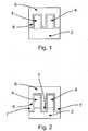
- FIG 2 shows an example of a capacitive environmental sensor.
- the sensor includes a substrate 2.
- the sensor also includes a plurality of electrodes 4 which are located on a surface of the substrate 2.
- the sensor also includes a sensor layer 6.
- the sensor layer 6 has a permittivity that is sensitive to the presence of a target substance.
- an interface layer comprising substances other than the target substance can build up at an interface between the electrodes 4 and the sensor layer 6.
- this interface layer is denoted using reference numeral 8.
- FIG. 2 is a simplified diagram showing only two electrodes 4 whereas, as a matter of practice, normally more than two electrodes may be provided.
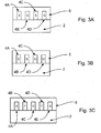
- Figures 3A to 3C illustrate a number of different electrical configurations for a plurality of electrodes in a sensor of the kind shown in Figure 2 .
- the term "electrical configuration" is used to refer to the potentials applied to the electrodes during measurements of capacitance.
- FIG 3A shows four electrodes 4A, 4B, 4C, 4D in a configuration that will be referred to herein as the "single spacing" configuration or the “single” configuration.
- a measurement of the capacitance of the electrodes is made by connecting the electrodes 4B and 4D to ground, while a signal (e.g. a DC potential) is applied to the electrodes 4A, 4C.
- S signal and ground connections
- Figure 3B shows an electrical configuration of the electrodes that will be referred to herein as the "double spacing" configuration or the “double” configuration.
- the electrodes 4A and 4B are connected to a signal potential, while the electrodes 4C and 4D are connected to ground.
- the single configuration includes neighbouring pairs of electrodes that include a first electrode connected to ground and a second electrode connected to a signal, whereby a potential difference appears across the neighbouring electrodes, while the double configuration, includes neighbouring pairs of electrodes that are connected either to a signal potential or to ground.
- Electrodes may be left floating.
- Floating electrodes are denoted in the figures as "F".
- the floating electrodes can be located in between the electrodes of a single or double configuration.
- Figure 3C shows an electrical configuration that may be referred to as the "single floating configuration".
- a set of electrodes 4A, 4C, 4E in the single configuration are interspersed with floating electrodes 4B, 4D.
- other floating configurations may be provided, for instance by interspersing electrodes having a double configuration as shown in Figure 3B with floating electrodes.
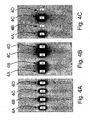
- Figures 4A to 4C show the electrical field line distributions produced by the electrical configurations shown in Figures 3A to 3C , respectively. It will be appreciated from a comparison of Figures 4B and 4C that the field lines produced by the double spacing configuration and the single floating configuration are similar. In the following description, the single spacing configurations such as that shown in Figure 3A and the double spacing configurations such as that shown in Figure 3B will be concentrated upon for illustrative purposes. Nevertheless, it is envisaged that electrode configurations including at least some floating electrodes fall within the scope of the claimed invention.
- a capacitive measurement can first be made with the electrodes having a first electrical configuration (for instance, the single configuration of Figure 3A ) and a second measurement of capacitance can then be made using electrodes having a second electrical configuration (for example, the double configuration shown in Figure 3B ).
- a first electrical configuration for instance, the single configuration of Figure 3A
- a second measurement of capacitance can then be made using electrodes having a second electrical configuration (for example, the double configuration shown in Figure 3B ).
- differential measurements can be made either by using a single set of electrodes that are switched between a plurality of different electrical configurations, or alternatively by using a plurality of different sets of electrodes that are each hard wired to have different electrical configurations.
- typically only a first and a second electrical configuration may be needed, with a separate measurement of capacitance being taken using each configuration.
- the measurements of capacitance made using each electrical configuration can be used to solve simultaneous equations relating to the various factors that affect the measurements of capacitance, thereby allowing the contribution to the measurement associated with the presence of the target substance to be isolated from other factors.
- the sensitivity of the electrodes in different electrical configurations can be modelled and simulated.
- the results of such modelling are described in respect of electrodes having the single configuration and the double configuration of Figures 3A and 3B , respectively.
- Table 1 shown below shows the sensitivities for the single and double electrode configurations of Figures 3A and 3B where the depth of the recesses 7 between each electrode is set to zero.
- Table 1 - Capacitive sensitivities for single and double electrode configurations at zero recess depth.
- each configuration i.e. the single configuration and the double configuration
- ⁇ C/ ⁇ sub where ⁇ sub is the permittivity of the substrate
- ⁇ C/ ⁇ sens where ⁇ sens is the permittivity of the sensor layer 6
- a scaling factor of 1.2 may be chosen to substantially reduce or remove sensitivity to the permittivity of the substrate (using a scaling factor of 1.2, it is shown in Table 1 that the value of ⁇ C/ ⁇ sub becomes 0.52).
- Figures 5 and 6 extend the simulation results of the kind shown in Table 1 by introducing a recess, having a non-zero depth, between each electrode as explained above in relation to Figure 2 .
- the sensitivity of the sensor to the thickness of the interface layer (t) is shown for a series of differential measurements.
- the differential measurement involves deducting a measurement taken in the double configuration from the measurement taken in the single configuration, with the application of a scaling factor.
- Figure 5B the sensitivity of the sensor to the target substance is shown using the same differential measurements and scaling factors used in Figure 5A . In this way, the effect of various scaling factors can be studied as a function of the depth of the recesses. Details of the various plots shown in Figures 5A and 5B are set out in Table 2 below. Table 2 - Differential Measurements in Figure 5.
- Figures 6A and 6B include plots that are summarised below in Table 3.
- Table 3 - Differential Measurements in Figure 6.
- Figure Reference Numeral Measurement 6A 32 Single - 1.0 * Double 6A 34 Single - 1.1 * Double 6A 36 Single - 1.3 * Double 6A 38 Single - 2.0 * Double 6B 42 Single - 1.0 * Double 6B 44 Single - 1.1 * Double 6B 46 Single - 1.3 * Double 6B 48 Single - 2.0 * Double
- plot 34 illustrates that a scaling factor of 1.1 applied to a differential measurement in which a measurement in the double configuration is deducted from a measurement taken in the single configuration, is suitable for removing sensitivity of the sensor to the permittivity of the substrate.
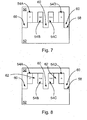
- FIG. 7 shows a capacitive environmental sensor in accordance with an embodiment of the invention.
- the sensor includes a semiconductor substrate 52.
- the substrate may, for example, comprise silicon.
- the substrate 52 has a surface 58.
- the substrate 52 may, in some examples, include a plurality of layers provided on an underlying silicon die.
- the plurality of layers may for instance include semiconductor layers for forming components such as transistors in the die, one or more metallization layers and one or more dielectric layers separating the metallization layers.
- the layers can also include one or more passivation layers.
- the surface 58 in the present example is the surface of an uppermost passivation layer of the substrate. In other examples, it is envisaged that the surface 58 may be the bare surface of a semiconductor die, without any intervening layers.
- the sensor includes a plurality of sensor electrodes 54A, 54B, 54C, 54D.
- the sensor electrodes 54A, 54B, 54C, 54D may be provided as a series of interdigitated fingers as is known in the art.
- the vertical thickness of the electrodes may be 0.1 ⁇ m ⁇ H ⁇ 10 ⁇ m.
- the electrodes may comprise any suitable electrically conductive material such as a metal or alloy (e.g. Al, W, Cu), possibly covered by a liner for adhesion purposes in fabrication, and moisture and corrosion barrier purposes during application (e.g. Ta 2 O 5 , Ti, TiN, SiOx or SiN).
- the liner may typically also cover the surface 58, in addition to the electrodes 54A, 54B, 54C, 54D whereby moisture may be prevented from entering the substrate 52.
- the sensor electrodes are located on the surface 58 of the substrate 52. As shown in Figure 7 , the sensor electrodes are laterally separated on the surface 58 by intervening spaces.
- the lateral width of the spacings may typically be 0.1 ⁇ m ⁇ W ⁇ 20 ⁇ m.
- the capacitive environmental sensor also includes a sensor layer 56.
- the sensor layer 56 covers the electrodes 54A, 54B, 54C, 54D.
- the sensor layer has a permittivity that is sensitive to the presence of the target substance.
- the target substance may, for example, comprise water (for example, where the capacitive environmental sensor is a humidity or moisture sensor), CO 2 or a volatile organic compound (VOC).
- the composition of the sensor layer 56 can be selected according to the target substance.
- the sensor layer 56 may comprise polymers like polyimide, parylene, or PDMS.
- the electrodes 54A, 54B, 54C, 54D in this example are switchable between two electrical configurations. In some embodiments, this switching can be controlled by a microcontroller, which may also collect and evaluate the measurements taken for each electrical configuration.
- a microcontroller which may also collect and evaluate the measurements taken for each electrical configuration.
- two separate groups of electrodes of the kind shown in Figure 7 may be placed in different locations on the substrate 52. The different sets or groups of electrodes may be located on completely different parts of the substrate 52 or may in some examples be places adjacent to each other.
- the first group of electrodes can have a first electrical configuration and the second group of electrodes can have the second electrical configuration for allowing differential measurements to be made between the two groups.
- the first electrical configuration in Figure 7 is a single spacing configuration in which the electrode 54B is switched to ground and the electrode 54C is switched to have a signal applied thereto (typically a DC potential).
- the electrical configuration in this state is thus "SGSG".
- the electrode 54 is switched to have a signal applied thereto, while the electrode 54C is switched to ground.
- the electrodes are connected as follows "SSGG", which will be recognised as the double spacing configuration described above.
- switching between the single spacing configuration and the double spacing configuration does not, in the present example, involve changing the state of the electrode 54A (which remains connected to "S") or the electrode 54D (which remains connected to "G").
- the surface 58 of the substrate 52 includes a number of recesses 60.
- the recesses 60 are located in some, but not all, of the spaces between the electrodes 54A, 54B, 54C, 54D. Accordingly, the surface 58 of the substrate 52, in a space separating at least one pair of electrodes in the present example, includes a recess, whereas the surface 58 of the substrate 52, in a space separating at least one pair of electrodes, does not include a recess.
- This arrangement of the recesses introduces a degree of asymmetry to the layout of the sensor. This asymmetry can, as will be demonstrated below, allow differential measurements to be made in a manner that does not substantially reduce or remove the sensitivity of the sensor to the target substance.
- Figure 8 shows a second embodiment of a capacitive environmental sensor.
- the sensor in Figure 8 is similar in many respects to the sensor described above in relation to Figure 7 .
- the main difference between the sensor shown in Figure 8 and the sensor described above in relation to Figure 7 is that in some of the spaces between the electrodes 54 in Figure 8 , the surface 58 of the substrate 52 extends upwards to at least partially fill the space between the electrodes 54.
- the space between the electrodes 54A and 54B is substantially filled by an upwardly extending portion 62 of the substrate 52.
- a portion 62 of the substrate 52 extends upwardly between the electrodes 54C and 54D.
- Figure 9 illustrates the results of simulations relating to a capacitive environmental sensor of the kind shown in Figure 7
- Figure 10 illustrates the results of similar simulations that have been carried out in relation to a sensor of the kind shown in Figure 8
- Figures 9 and 10 both illustrate that when arrangements of the kind shown in Figures 7 and 8 are used, sensitivity to the presence of an interface layer can be factored out while retaining sensitivity to a target substance.
- the sensor layer is assumed to consist of polyimide with a nominal dielectric constant ( ⁇ ) of 3, and showing typical variations of approximately +-20% over the full relative humidity range.
- Substrate permittivity is assumed to be 4.2, representing SiO 2 .
- the depth of the recesses 60 can be selected along with the appropriate scaling factor so that the sensitivity of the sensor to a factor other than the presence of the target substance can be reduced or removed.
- the points A, B, C in Figures 9A and 9B represent three corresponding choices of recess depth and scaling factor. Taking the example of point B, the recess depth is approximately 0.4 ⁇ m and the scaling factor is selected to be 2.4 (see plot 74). Figure 9A shows that these values, sensitivity to the interface layer is approximately zero.
- a first measurement can be made in the single spaced electrode configuration and then a second measurement can be made in the double spaced electrode configuration.
- the result of the measurement in the double spaced electrode configuration may then be multiplied by the scaling factor of 2.4 and deducted from the result in the single spaced electrode configuration.
- This result will not be sensitive to the interface layer as is clear from Figure 9A .
- Figure 9B and referring to point B shown therein, which corresponds to the same recess depth (approximately 0.4 ⁇ m) and scaling factor (2.4), it can be seen that the sensor is still sensitive to the presence of the target substance.
- Point C in Figures 9A and 9B is an alternative choice of parameters in which the recess depth is slightly greater (approximately 0.7 ⁇ m) and the scaling factor is 2.7. It can be seen that point C in Figure 9B provides an even greater sensitivity to the presence of the target substance then point B, while reducing sensitivity to the interface layer.
- Figures 10A and 10B show results that are similar to those described above in relation to Figures 9A and 9B except that they apply to the embodiment of Figure 8 .
- Each of points A, B and C in Figures 10A and 10B represent different choices of recess depth and respective scaling factors.
- the embodiment of Figure 8 can allow sensitivity to the interface layer to be reduced or removed by while retaining an enhanced sensitivity to the target substance compared to the embodiment of Figure 7 .
- Figures 11 and 12 illustrate the results of simulations similar to those described above in relation to Figures 9 and 10 , except that they demonstrate the reduction or removal of the sensitivity of the device to the permittivity of the substrate.
- the results in Figure 11 correspond to a device of the kind described above in relation to Figure 7
- the results in Figure 12 correspond to a sensor of the kind described above in relation to Figure 8 .
- Table 6 summarises the various plots in Figures 11A and 11B and the scaling factors used. Table 6 - Measurements in Figure 11.
- each of points A, B and C are chosen such that the sensitivity to the permittivity of the substrate is approximately zero.
- Figure 11B it can be seen that for each of points A, B and C (which correspond to the same recess depths and scaling factors used in the points A, B and C in Figure 11A ), the sensitivity of the sensor to the target substance is retained during the differential measurement.
- points A and C may be preferred to point B, since the retained sensitivity of the sensor to the target substance is substantially greater at points A and C than at point B.
- Figure 11 demonstrates that, by appropriate selection of the depth of the recess and corresponding scaling factor, sensitivity of the sensor to the target substance can be retained while reducing or removing sensitivity of the sensor to the permittivity of the substrate.
- Table 7 summarises the various plots in Figure 12 and the scaling factors used. Table 7 - Measurements in Figure 12.
- FIG 12B it can be seen that at both points A and B, the sensitivity of the sensor to the target substance is retained.
- Comparison of Figure 12B with Figure 11B reveals that the sensitivity of the sensor in Figure 8 compared to the sensitivity of the sensor in Figure 7 to the target substance is somewhat larger in the case of sensor of Figure 8 .
- an arrangement in which the substrate, in a space separating at least one pair of electrodes, extends upwardly to at least partially fill the space can further enhance the extent to which the sensitivity to the target substance can be retained while removing sensitivity to factors other than the target substance.
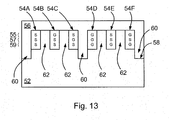
- FIG. 13 shows an example of a capacitive environmental sensor according to another embodiment of this invention.
- the sensor is similar in many respects to the sensors described above in relation to Figures 7 and 8 and like reference numerals have been used.
- the sensor shown in Figure 13 differs from the examples of Figures 7 and 8 as follows.
- the electrodes 54 in Figure 13 are switchable between three different electrical configurations. These electrical configurations are shown in Figure 13 using reference numerals 55, 57 and 59.
- the electrical configuration 55 is a single spaced configuration of the kind described above in which the electrodes 54A, 54B, 54C, 54D, 54E, 54F are connected either to a signal or to ground as follows "SGSGSG”.
- the electrical configuration 57 shown in Figure 13 is the double space configuration in which the electrodes are connected to signal or to ground as follows "SSGGSS”.
- the third electrical configuration 59 shown in Figure 13 is referred to herein as the "triple spaced configuration" or the "triple” configuration. In the triple spaced configuration the electrodes are connected to signal or ground as follows "SSSGGG". It is noted that while the single spaced configuration in principle requires a minimum of two electrodes and the double spaced configuration requires a minimum of four electrodes, a minimum of six electrodes are required to support the triple spaced configuration.
- the recesses 60 in a surface 58 of a substrate 52 are provided at every third electrode spacing in contrast to the examples described above in relation to Figures 7 and 8 in which the recesses 60 are provided in every second electrode spacing.
- Double Signa l Double + Drif t Double + noisys e Double
- Differential cos ⁇ Single + sin ⁇ Double
- noisy e Differential cos ⁇ noisy e Single + sin ⁇ noisy e Double
- k can be chosen such that the sign of Signal Differential is equal to that of Signal Single .
- Signa l Differential Signa l Single
- 1 1 + 1 m Drift 2 Signa l Single
- ⁇ Optimal can be chosen using a test or calibration system. Testing and calibration may be performed for each sensor individually. Alternatively, a representative sample of sensors may be used to derive parameters for use across a larger batch. The values can be stored in the sensor (e.g. in a reference table accessible by a microcontroller). These calibration values can also be stored across a range of operating conditions (e.g. different temperatures, pressures and so on) and used accordingly to the environment in which the sensor is located.
- operating conditions e.g. different temperatures, pressures and so on
- the number of measurements made may more than strictly required to compensate for factors other than the sensitivity of the sensor to the target substance.
- a relatively large number of capacitive measurements may be made in a plurality of respective electrical configurations of the electrodes.
- three or more capacitive measurements may be made in respective electrical configurations of the electrodes for accounting for a single factor such as the presence of an interface layer or changing permittivity of the substrate.
- four or more capacitive measurements may be made in respective electrical configurations of the electrodes for compensating for two factors such as the presence of an interface layer or changing permittivity of the substrate.
- a corrected N-dimensional vector y Ax of corrected values with N smaller than or equal to M, where A is a N-by-K matrix of weight factors (N rows and K columns).
- the optimal matrix A can be found as follows.
- the elements of y represent the actual values of the parameters to be determined (e.g. humidity, CO2 concentration, etc.).
- the k-th measurement x(k) taken with a k-th electrical configuration of the electrodes, is equal to b(k)y+r(k), where the first term is an ideal model response (in the absence of noise and other disturbing processes) and the second term is a disturb in the k-th measurement.
- the ideal case i.e.
- the required model matrix C can be calculated, determined experimentally with a (typically large) set of calibration measurements under controlled environmental conditions (i.e. known vectors y), or a combination of both. C can also be made dependent on the history of the sensor (e.g. its age, or the ensemble of gasses it has previously detected) to accommodate for aging and/or degradation of the sensor (of course this requires an aging/degradation model).
- the matrix C may also be initially fixed when the sensor is sold, and later be updated to a better version, or updated to a more advanced matrix that includes an aging/degradation model. This approach can be used to improve the quality of already sold products with in-system updates, which is a frequently used approach for modern devices, especially for portable devices like mobile phones.
- Embodiments of this invention can be used in applications that required the sensing of substances such as moisture, gases such as CO2 or volatile organic compounds. It is envisaged that a sensor of the kind described herein may be incorporated into a radio frequency identification (RFID) tag to support applications of this kind. It is further envisaged that a sensor of the kind described herein may be used in a smart building or in devices such as a mobile telephone or table. The smart building may be a greenhouse.
- RFID radio frequency identification
- the sensor includes a semiconductor substrate having a surface.
- the sensor also includes a plurality of sensor electrodes located on the surface. The electrodes are laterally separated on the surface by intervening spaces.
- the sensor further includes a sensor layer covering the electrodes.
- the sensor layer has a permittivity that is sensitive to the presence of the target substance.
- the surface of the substrate, in a space separating at least one pair of electrodes includes a recess.
- the surface of the substrate, in a space separating at least one pair of electrodes does not include a recess.
- the sensor may be provided in a Radio Frequency Identification (RFID) tag.
- RFID Radio Frequency Identification
Claims (13)
- Kapazitiver Umweltsensor, umfassend:- ein Halbleitersubstrat (52) mit einer Oberfläche (58);- mehrere Sensorelektroden (54), die sich auf der Oberfläche in einer einzelnen Elektrodenebene befinden, wobei jedes Paar benachbarter Elektroden auf der Oberfläche durch einen jeweiligen dazwischenliegenden Raum seitlich getrennt sind; und- eine die Elektroden bedeckende Sensorschicht (56), wobei die Sensorschicht eine Permittivität hat, die empfindlich für das Vorhandensein einer Zielsubstanz ist;- wobei die Oberfläche des Substrats in dem jeweiligen dazwischenliegenden Raum, der mindestens ein Paar Elektroden trennt, eine Ausnehmung enthält, wobei die Oberfläche des Substrats in dem Raum, der mindestens ein anderes Paar Elektroden trennt, keine Ausnehmung enthält;- und wobei entweder:(a) die Elektroden mehrere separate Gruppen von auf dem Substrat angeordneten Elektroden enthalten, wobei jede Gruppe eine andere elektrische Konfiguration hat, um differenzielle kapazitive Messungen zwischen jeder Gruppe durchzuführen;
oder(b) die Elektroden zwischen mehreren verschiedenen elektrischen Konfigurationen umschaltbar sind, um differenzielle kapazitive Messungen durchzuführen. - Kapazitiver Umweltsensor nach Anspruch 1, wobei die Räume, in denen die Oberfläche des Substrats eine Ausnehmung enthält, sich in einer periodischen Abfolge mit den Räumen abwechseln, in denen die Oberfläche des Substrats keine Ausnehmung enthält.
- Kapazitiver Umweltsensor nach Anspruch 2, wobei sich das Substrat in mindestens einem ein Paar Elektroden trennenden Raum, der keine Ausnehmung enthält, nach oben erstreckt, um den Raum zumindest teilweise zu füllen.
- Kapazitiver Umweltsensor nach Anspruch 3, wobei die periodische Abfolge in der Form 'XZXZX' vorliegt, worin 'X' einen Raum bezeichnet, der eine Ausnehmung enthält, und worin 'Z' einen Raum bezeichnet, in dem sich das Substrat nach oben erstreckt, um den Raum zumindest teilweise zu füllen.
- Kapazitiver Umweltsensor nach Anspruch 3, wobei die periodische Abfolge in der Form 'XZZXZZX' vorliegt, worin 'X' einen Raum bezeichnet, der eine Ausnehmung enthält, und worin 'Z' einen Raum bezeichnet, der keine Ausnehmung enthält.
- Kapazitiver Umweltsensor nach Anspruch 3, wobei die periodische Abfolge in der Form 'XYXYX' vorliegt, worin 'X' einen Raum bezeichnet, der eine Ausnehmung enthält, und worin 'Y' einen Raum bezeichnet, der keine Ausnehmung enthält.
- Kapazitiver Umweltsensor nach einem der vorhergehenden Ansprüche, der eingerichtet ist, eine differenzielle kapazitive Messung zum Bestimmen des Vorhandenseins der Zielsubstanz durchzuführen durch:- Durchführen einer ersten Messung der Kapazität zumindest einiger der Elektroden in einer ersten elektrischen Konfiguration;- Durchführen einer zweiten Messung der Kapazität zumindest einiger der Elektroden in einer zweiten elektrischen Konfiguration;- Anlegen eines Skalierungsfaktors an die zweite Messung, um die Empfindlichkeit des Sensors auf einen anderen Faktor als das Vorhandensein der Zielsubstanz zu kompensieren; und- Bestimmen des Vorhandenseins der Zielsubstanz, indem die Differenz zwischen der ersten Messung und der zweiten Messung verglichen wird.
- Kapazitiver Umweltsensor nach Anspruch 7, wobei das Durchführen der differenziellen kapazitiven Messung darüber hinaus umfasst:- Durchführen einer dritten Messung der Kapazität zumindest einiger der Elektroden in einer dritten elektrischen Konfiguration;- Anlegen eines Skalierungsfaktors an die dritte Messung, um die Empfindlichkeit des Sensors auf einen anderen Faktor als das Vorhandensein der Zielsubstanz zu kompensieren, und- Bestimmen des Vorhandenseins der Zielsubstanz, indem die Differenzen zwischen der ersten, zweiten und dritten Messung verglichen werden.
- Kapazitiver Umweltsensor nach einem der Ansprüche 1 bis 6, der eingerichtet ist, eine differenzielle kapazitive Messung zum Bestimmen des Vorhandenseins der Zielsubstanz durchzuführen durch:- Durchführen mehrerer Messungen der Kapazität von mindestens einigen der Elektroden in jeweiligen unterschiedlichen Elektrodenkonfigurationen;- Anlegen eines Skalierungsfaktors an zumindest einige der Messungen, um die Empfindlichkeit des Sensors auf einen anderen Faktor als das Vorhandensein der Zielsubstanz zu kompensieren, und- Bestimmen des Vorhandenseins der Zielsubstanz, indem die Differenzen zwischen den Messungen ausgewertet werden,- wobei es sich bei der Anzahl von durchgeführten Kapazitätsmessungen um mindestens zwei mehr als die Anzahl von kompensierten anderen Faktoren als das Vorhandensein der Zielsubstanz handelt.
- Kapazitiver Umweltsensor nach einem der vorhergehenden Ansprüche, wobei das Substrat mehrere Schichten enthält, und wobei sich die Sensorelektroden auf einer Oberfläche einer der mehreren Schichten befinden.
- Kapazitiver Umweltsensor nach einem der vorhergehenden Ansprüche, wobei die Zielsubstanz Wasser, CO2 oder eine flüchtige organische Verbindung (VOC) umfasst.
- Intelligentes Gebäude mit dem kapazitiven Umweltsensor nach einem der Ansprüche 1 bis 11.
- Verfahren zum Bestimmen des Vorhandenseins einer Zielsubstanz anhand von differenziellen kapazitiven Messungen, wobei das Verfahren umfasst:- Bereitstellen eines kapazitiven Umweltsensors nach einem der Ansprüche 1 bis 11;- Durchführen einer ersten Messung der Kapazität zumindest einiger der Elektroden in einer ersten elektrischen Konfiguration;- Durchführen einer zweiten Messung der Kapazität zumindest einiger der Elektroden in einer zweiten elektrischen Konfiguration;- Anlegen eines Skalierungsfaktors an die zweite Messung, um die Empfindlichkeit des Sensors auf einen anderen Faktor als das Vorhandensein der Zielsubstanz zu kompensieren; und- Bestimmen des Vorhandenseins der Zielsubstanz, indem die Differenz zwischen der ersten und der zweiten Messung verglichen wird.
Priority Applications (6)
| Application Number | Priority Date | Filing Date | Title |
|---|---|---|---|
| EP14181602.5A EP2988122B1 (de) | 2014-08-20 | 2014-08-20 | Kapazitiver Sensor |
| PCT/EP2015/068691 WO2016026771A1 (en) | 2014-08-20 | 2015-08-13 | Capacitive sensor |
| KR1020177007357A KR101946177B1 (ko) | 2014-08-20 | 2015-08-13 | 용량 센서 |
| JP2017507833A JP6285077B2 (ja) | 2014-08-20 | 2015-08-13 | 容量式センサ |
| CN201580044629.9A CN106796192B (zh) | 2014-08-20 | 2015-08-13 | 电容式传感器 |
| US15/505,068 US10274450B2 (en) | 2014-08-20 | 2015-08-13 | Capacitive sensor |
Applications Claiming Priority (1)
| Application Number | Priority Date | Filing Date | Title |
|---|---|---|---|
| EP14181602.5A EP2988122B1 (de) | 2014-08-20 | 2014-08-20 | Kapazitiver Sensor |
Publications (2)
| Publication Number | Publication Date |
|---|---|
| EP2988122A1 EP2988122A1 (de) | 2016-02-24 |
| EP2988122B1 true EP2988122B1 (de) | 2019-04-24 |
Family
ID=51357861
Family Applications (1)
| Application Number | Title | Priority Date | Filing Date |
|---|---|---|---|
| EP14181602.5A Active EP2988122B1 (de) | 2014-08-20 | 2014-08-20 | Kapazitiver Sensor |
Country Status (6)
| Country | Link |
|---|---|
| US (1) | US10274450B2 (de) |
| EP (1) | EP2988122B1 (de) |
| JP (1) | JP6285077B2 (de) |
| KR (1) | KR101946177B1 (de) |
| CN (1) | CN106796192B (de) |
| WO (1) | WO2016026771A1 (de) |
Families Citing this family (15)
| Publication number | Priority date | Publication date | Assignee | Title |
|---|---|---|---|---|
| EP3208610B1 (de) | 2016-02-18 | 2021-05-12 | ams AG | Sensoranordnung und verfahren zur erzeugung von messsignalen |
| US10005108B2 (en) | 2016-10-17 | 2018-06-26 | Robert Bosch Gmbh | Lens cleaning method for a surveillance camera |
| US10274449B2 (en) * | 2016-10-17 | 2019-04-30 | Robert Bosch Gmbh | Capacitive moisture sensor system for a surveillance camera |
| CN107478692A (zh) * | 2017-08-16 | 2017-12-15 | 温州市洞头信达电器有限公司 | 一种传感器 |
| CN107589155A (zh) * | 2017-09-12 | 2018-01-16 | 华南师范大学 | 一种电容式传感器及其制备方法 |
| JP6696552B2 (ja) | 2017-11-13 | 2020-05-20 | 株式会社村田製作所 | 配線容量キャンセル方法および配線容量キャンセル装置 |
| JP2021047015A (ja) * | 2018-01-16 | 2021-03-25 | アルプスアルパイン株式会社 | 湿度検知装置 |
| KR102519643B1 (ko) * | 2018-02-13 | 2023-04-10 | 엘지이노텍 주식회사 | 감지 장치 및 이를 포함하는 와이퍼 구동 장치 |
| EP3540422B1 (de) | 2018-03-14 | 2024-01-03 | Sciosense B.V. | Monolithische gassensoranordnung, herstellungsverfahren und messverfahren |
| SE541636C2 (en) | 2018-03-29 | 2019-11-19 | Foolproof Ab | Fluid detector label and fluid detector system comprising at least one such label |
| DE102018210387B4 (de) * | 2018-06-26 | 2023-03-23 | Robert Bosch Gmbh | Sensorvorrichtung und Verfahren zum Detektieren von Gasen |
| US11562582B2 (en) * | 2018-12-03 | 2023-01-24 | Ams International Ag | Three dimensional imaging with intensity information |
| CN209326840U (zh) | 2018-12-27 | 2019-08-30 | 热敏碟公司 | 压力传感器及压力变送器 |
| US11604164B2 (en) * | 2020-12-14 | 2023-03-14 | Molex, Llc | Photoionization detector and method of operating same |
| CN115166373B (zh) * | 2022-07-01 | 2024-03-26 | 同济大学 | 一种低真空下的聚合物薄膜复介电系数测量装置和方法 |
Family Cites Families (19)
| Publication number | Priority date | Publication date | Assignee | Title |
|---|---|---|---|---|
| JPS57148242A (en) | 1981-03-09 | 1982-09-13 | Nissan Motor Co Ltd | Electrostatic capacity sensor |
| JP2646690B2 (ja) | 1988-08-23 | 1997-08-27 | 株式会社デンソー | 雨滴センサ |
| US6373263B1 (en) | 2000-04-20 | 2002-04-16 | Millennium Sensors Ltd. | Differential windshield capacitive rain sensor |
| DE10049901C2 (de) * | 2000-10-10 | 2003-01-02 | Aventis Res & Tech Gmbh & Co | Vorrichtung und Verfahren zur elektrisch beschleunigten Immobilisierung und zur Detektion von Molekülen |
| JP4501320B2 (ja) * | 2001-07-16 | 2010-07-14 | 株式会社デンソー | 容量式湿度センサ |
| DE10134938A1 (de) | 2001-07-18 | 2003-02-06 | Bosch Gmbh Robert | Halbleiterbauelement sowie ein Verfahren zur Herstellung des Halbleiterbauelements |
| JP3704685B2 (ja) | 2002-07-29 | 2005-10-12 | 株式会社山武 | 静電容量センサ |
| EP1607739B1 (de) | 2004-06-18 | 2013-07-03 | Sensirion AG | Kapazitiver Sensor |
| JP4229885B2 (ja) * | 2004-08-18 | 2009-02-25 | 株式会社デンソー | 容量式物理量検出装置 |
| JP4458135B2 (ja) | 2007-03-27 | 2010-04-28 | 株式会社デンソー | 液体性状センサ |
| MY164505A (en) * | 2007-11-23 | 2017-12-29 | Mimos Berhad | Capacitive sensor |
| MY154211A (en) | 2011-04-26 | 2015-05-15 | Mimos Berhad | A humidity sensor device |
| JP5516505B2 (ja) | 2011-05-25 | 2014-06-11 | 株式会社デンソー | 容量式湿度センサ及びその製造方法 |
| EP2565635B1 (de) | 2011-09-02 | 2017-11-15 | Sensirion AG | Sensorchip und Verfahren zur Herstellung eines Sensorchips |
| JP2013190286A (ja) | 2012-03-13 | 2013-09-26 | Azbil Corp | センサ装置 |
| US20140026642A1 (en) | 2012-07-25 | 2014-01-30 | John O. O'Connell | Capacitive sensor comprising differing unit cell structures |
| JP6031889B2 (ja) | 2012-08-22 | 2016-11-24 | 富士通株式会社 | 計測装置及び計測方法 |
| KR20150028929A (ko) * | 2013-09-06 | 2015-03-17 | 매그나칩 반도체 유한회사 | 정전용량형 습도센서 |
| CN103487474B (zh) | 2013-09-30 | 2016-08-17 | 东南大学 | 一种具有高灵敏度快速响应的mems电容式湿度传感器 |
-
2014
- 2014-08-20 EP EP14181602.5A patent/EP2988122B1/de active Active
-
2015
- 2015-08-13 US US15/505,068 patent/US10274450B2/en active Active
- 2015-08-13 JP JP2017507833A patent/JP6285077B2/ja active Active
- 2015-08-13 KR KR1020177007357A patent/KR101946177B1/ko active IP Right Grant
- 2015-08-13 WO PCT/EP2015/068691 patent/WO2016026771A1/en active Application Filing
- 2015-08-13 CN CN201580044629.9A patent/CN106796192B/zh active Active
Non-Patent Citations (1)
| Title |
|---|
| None * |
Also Published As
| Publication number | Publication date |
|---|---|
| CN106796192A (zh) | 2017-05-31 |
| JP6285077B2 (ja) | 2018-02-28 |
| EP2988122A1 (de) | 2016-02-24 |
| US20170261457A1 (en) | 2017-09-14 |
| JP2017525959A (ja) | 2017-09-07 |
| CN106796192B (zh) | 2019-10-29 |
| WO2016026771A1 (en) | 2016-02-25 |
| US10274450B2 (en) | 2019-04-30 |
| KR101946177B1 (ko) | 2019-04-17 |
| KR20170043604A (ko) | 2017-04-21 |
Similar Documents
| Publication | Publication Date | Title |
|---|---|---|
| EP2988122B1 (de) | Kapazitiver Sensor | |
| US8121800B2 (en) | Capacitative node measurement in a capacitative matrix pressure inducer | |
| Rivadeneyra et al. | Design and characterization of a low thermal drift capacitive humidity sensor by inkjet-printing | |
| US7943394B2 (en) | Method and device for high sensitivity detection of the presence of DNA and other probes | |
| US9121826B2 (en) | Noise shielding techniques for ultra low current measurements in biochemical applications | |
| TWI612852B (zh) | 用於電漿腔室之處理條件感測裝置及方法 | |
| US9287219B2 (en) | Radiation-blocking structures | |
| US20140026642A1 (en) | Capacitive sensor comprising differing unit cell structures | |
| CN101896814A (zh) | 传感器、传感器阵列以及操作传感器的方法 | |
| JP2009092633A (ja) | インピーダンスセンサ | |
| CN108700540B (zh) | 用于生成测量信号的传感器装置和方法 | |
| US20020193957A1 (en) | Data collection methods and apparatus with parasitic correction | |
| US10871862B2 (en) | Touch force detecting method and apparatus, touch panel and display apparatus | |
| KR20180033053A (ko) | 센서 장치 | |
| US20180188201A1 (en) | Bio-sensor and bio-sensor array | |
| EP3599447B1 (de) | Dielektrizitätskonstanten-unempfindlicher flüssigkeitspegelsensor zum direkten einführen in eine flüssigkeit mit hoher dielektrizitätskonstante | |
| CA2510720C (en) | Dna chip comprising a microarray made of microelectrode systems | |
| JP5397333B2 (ja) | 半導体装置、並びに、センサ素子及び半導体装置の製造方法 | |
| CN114705724A (zh) | 无漂移湿度传感器 | |
| Kjaer et al. | Characterization of positional errors and their influence on micro four-point probe measurements on a 100 nm Ru film | |
| US20230288367A1 (en) | Detection device, detection method, learning device, and detection device manufacturing method | |
| Baeuscher et al. | Investigation of IDC Structures for Graphene Based Biosensors Using Low Frequency EIS Method | |
| KR20220081658A (ko) | 일체형 생화학 센서 및 그 제조방법 | |
| CN111521546A (zh) | 一种细胞传感器阵列和细胞检测芯片 |
Legal Events
| Date | Code | Title | Description |
|---|---|---|---|
| PUAI | Public reference made under article 153(3) epc to a published international application that has entered the european phase |
Free format text: ORIGINAL CODE: 0009012 |
|
| AK | Designated contracting states |
Kind code of ref document: A1 Designated state(s): AL AT BE BG CH CY CZ DE DK EE ES FI FR GB GR HR HU IE IS IT LI LT LU LV MC MK MT NL NO PL PT RO RS SE SI SK SM TR |
|
| AX | Request for extension of the european patent |
Extension state: BA ME |
|
| 17P | Request for examination filed |
Effective date: 20160719 |
|
| RBV | Designated contracting states (corrected) |
Designated state(s): AL AT BE BG CH CY CZ DE DK EE ES FI FR GB GR HR HU IE IS IT LI LT LU LV MC MK MT NL NO PL PT RO RS SE SI SK SM TR |
|
| GRAP | Despatch of communication of intention to grant a patent |
Free format text: ORIGINAL CODE: EPIDOSNIGR1 |
|
| STAA | Information on the status of an ep patent application or granted ep patent |
Free format text: STATUS: GRANT OF PATENT IS INTENDED |
|
| INTG | Intention to grant announced |
Effective date: 20181205 |
|
| GRAS | Grant fee paid |
Free format text: ORIGINAL CODE: EPIDOSNIGR3 |
|
| GRAA | (expected) grant |
Free format text: ORIGINAL CODE: 0009210 |
|
| STAA | Information on the status of an ep patent application or granted ep patent |
Free format text: STATUS: THE PATENT HAS BEEN GRANTED |
|
| RIN1 | Information on inventor provided before grant (corrected) |
Inventor name: NENADOVIC, NEBOJSA Inventor name: ZIVKOVIC, ZORAN Inventor name: WIDDERSHOVEN, FRANCISCUS PETRUS Inventor name: HILCO, SUY |
|
| AK | Designated contracting states |
Kind code of ref document: B1 Designated state(s): AL AT BE BG CH CY CZ DE DK EE ES FI FR GB GR HR HU IE IS IT LI LT LU LV MC MK MT NL NO PL PT RO RS SE SI SK SM TR |
|
| REG | Reference to a national code |
Ref country code: GB Ref legal event code: FG4D |
|
| REG | Reference to a national code |
Ref country code: CH Ref legal event code: EP |
|
| REG | Reference to a national code |
Ref country code: AT Ref legal event code: REF Ref document number: 1124721 Country of ref document: AT Kind code of ref document: T Effective date: 20190515 Ref country code: IE Ref legal event code: FG4D |
|
| REG | Reference to a national code |
Ref country code: DE Ref legal event code: R096 Ref document number: 602014045220 Country of ref document: DE |
|
| REG | Reference to a national code |
Ref country code: NL Ref legal event code: MP Effective date: 20190424 |
|
| REG | Reference to a national code |
Ref country code: LT Ref legal event code: MG4D |
|
| PG25 | Lapsed in a contracting state [announced via postgrant information from national office to epo] |
Ref country code: NL Free format text: LAPSE BECAUSE OF FAILURE TO SUBMIT A TRANSLATION OF THE DESCRIPTION OR TO PAY THE FEE WITHIN THE PRESCRIBED TIME-LIMIT Effective date: 20190424 |
|
| PG25 | Lapsed in a contracting state [announced via postgrant information from national office to epo] |
Ref country code: FI Free format text: LAPSE BECAUSE OF FAILURE TO SUBMIT A TRANSLATION OF THE DESCRIPTION OR TO PAY THE FEE WITHIN THE PRESCRIBED TIME-LIMIT Effective date: 20190424 Ref country code: NO Free format text: LAPSE BECAUSE OF FAILURE TO SUBMIT A TRANSLATION OF THE DESCRIPTION OR TO PAY THE FEE WITHIN THE PRESCRIBED TIME-LIMIT Effective date: 20190724 Ref country code: PT Free format text: LAPSE BECAUSE OF FAILURE TO SUBMIT A TRANSLATION OF THE DESCRIPTION OR TO PAY THE FEE WITHIN THE PRESCRIBED TIME-LIMIT Effective date: 20190824 Ref country code: AL Free format text: LAPSE BECAUSE OF FAILURE TO SUBMIT A TRANSLATION OF THE DESCRIPTION OR TO PAY THE FEE WITHIN THE PRESCRIBED TIME-LIMIT Effective date: 20190424 Ref country code: SE Free format text: LAPSE BECAUSE OF FAILURE TO SUBMIT A TRANSLATION OF THE DESCRIPTION OR TO PAY THE FEE WITHIN THE PRESCRIBED TIME-LIMIT Effective date: 20190424 Ref country code: HR Free format text: LAPSE BECAUSE OF FAILURE TO SUBMIT A TRANSLATION OF THE DESCRIPTION OR TO PAY THE FEE WITHIN THE PRESCRIBED TIME-LIMIT Effective date: 20190424 Ref country code: LT Free format text: LAPSE BECAUSE OF FAILURE TO SUBMIT A TRANSLATION OF THE DESCRIPTION OR TO PAY THE FEE WITHIN THE PRESCRIBED TIME-LIMIT Effective date: 20190424 Ref country code: ES Free format text: LAPSE BECAUSE OF FAILURE TO SUBMIT A TRANSLATION OF THE DESCRIPTION OR TO PAY THE FEE WITHIN THE PRESCRIBED TIME-LIMIT Effective date: 20190424 |
|
| PG25 | Lapsed in a contracting state [announced via postgrant information from national office to epo] |
Ref country code: BG Free format text: LAPSE BECAUSE OF FAILURE TO SUBMIT A TRANSLATION OF THE DESCRIPTION OR TO PAY THE FEE WITHIN THE PRESCRIBED TIME-LIMIT Effective date: 20190724 Ref country code: PL Free format text: LAPSE BECAUSE OF FAILURE TO SUBMIT A TRANSLATION OF THE DESCRIPTION OR TO PAY THE FEE WITHIN THE PRESCRIBED TIME-LIMIT Effective date: 20190424 Ref country code: RS Free format text: LAPSE BECAUSE OF FAILURE TO SUBMIT A TRANSLATION OF THE DESCRIPTION OR TO PAY THE FEE WITHIN THE PRESCRIBED TIME-LIMIT Effective date: 20190424 Ref country code: GR Free format text: LAPSE BECAUSE OF FAILURE TO SUBMIT A TRANSLATION OF THE DESCRIPTION OR TO PAY THE FEE WITHIN THE PRESCRIBED TIME-LIMIT Effective date: 20190725 Ref country code: LV Free format text: LAPSE BECAUSE OF FAILURE TO SUBMIT A TRANSLATION OF THE DESCRIPTION OR TO PAY THE FEE WITHIN THE PRESCRIBED TIME-LIMIT Effective date: 20190424 |
|
| REG | Reference to a national code |
Ref country code: AT Ref legal event code: MK05 Ref document number: 1124721 Country of ref document: AT Kind code of ref document: T Effective date: 20190424 |
|
| PG25 | Lapsed in a contracting state [announced via postgrant information from national office to epo] |
Ref country code: IS Free format text: LAPSE BECAUSE OF FAILURE TO SUBMIT A TRANSLATION OF THE DESCRIPTION OR TO PAY THE FEE WITHIN THE PRESCRIBED TIME-LIMIT Effective date: 20190824 |
|
| REG | Reference to a national code |
Ref country code: DE Ref legal event code: R097 Ref document number: 602014045220 Country of ref document: DE |
|
| PG25 | Lapsed in a contracting state [announced via postgrant information from national office to epo] |
Ref country code: RO Free format text: LAPSE BECAUSE OF FAILURE TO SUBMIT A TRANSLATION OF THE DESCRIPTION OR TO PAY THE FEE WITHIN THE PRESCRIBED TIME-LIMIT Effective date: 20190424 Ref country code: SK Free format text: LAPSE BECAUSE OF FAILURE TO SUBMIT A TRANSLATION OF THE DESCRIPTION OR TO PAY THE FEE WITHIN THE PRESCRIBED TIME-LIMIT Effective date: 20190424 Ref country code: CZ Free format text: LAPSE BECAUSE OF FAILURE TO SUBMIT A TRANSLATION OF THE DESCRIPTION OR TO PAY THE FEE WITHIN THE PRESCRIBED TIME-LIMIT Effective date: 20190424 Ref country code: EE Free format text: LAPSE BECAUSE OF FAILURE TO SUBMIT A TRANSLATION OF THE DESCRIPTION OR TO PAY THE FEE WITHIN THE PRESCRIBED TIME-LIMIT Effective date: 20190424 Ref country code: AT Free format text: LAPSE BECAUSE OF FAILURE TO SUBMIT A TRANSLATION OF THE DESCRIPTION OR TO PAY THE FEE WITHIN THE PRESCRIBED TIME-LIMIT Effective date: 20190424 Ref country code: DK Free format text: LAPSE BECAUSE OF FAILURE TO SUBMIT A TRANSLATION OF THE DESCRIPTION OR TO PAY THE FEE WITHIN THE PRESCRIBED TIME-LIMIT Effective date: 20190424 |
|
| PG25 | Lapsed in a contracting state [announced via postgrant information from national office to epo] |
Ref country code: IT Free format text: LAPSE BECAUSE OF FAILURE TO SUBMIT A TRANSLATION OF THE DESCRIPTION OR TO PAY THE FEE WITHIN THE PRESCRIBED TIME-LIMIT Effective date: 20190424 Ref country code: SM Free format text: LAPSE BECAUSE OF FAILURE TO SUBMIT A TRANSLATION OF THE DESCRIPTION OR TO PAY THE FEE WITHIN THE PRESCRIBED TIME-LIMIT Effective date: 20190424 |
|
| PLBE | No opposition filed within time limit |
Free format text: ORIGINAL CODE: 0009261 |
|
| STAA | Information on the status of an ep patent application or granted ep patent |
Free format text: STATUS: NO OPPOSITION FILED WITHIN TIME LIMIT |
|
| PG25 | Lapsed in a contracting state [announced via postgrant information from national office to epo] |
Ref country code: TR Free format text: LAPSE BECAUSE OF FAILURE TO SUBMIT A TRANSLATION OF THE DESCRIPTION OR TO PAY THE FEE WITHIN THE PRESCRIBED TIME-LIMIT Effective date: 20190424 |
|
| 26N | No opposition filed |
Effective date: 20200127 |
|
| PG25 | Lapsed in a contracting state [announced via postgrant information from national office to epo] |
Ref country code: LU Free format text: LAPSE BECAUSE OF NON-PAYMENT OF DUE FEES Effective date: 20190820 Ref country code: SI Free format text: LAPSE BECAUSE OF FAILURE TO SUBMIT A TRANSLATION OF THE DESCRIPTION OR TO PAY THE FEE WITHIN THE PRESCRIBED TIME-LIMIT Effective date: 20190424 Ref country code: MC Free format text: LAPSE BECAUSE OF FAILURE TO SUBMIT A TRANSLATION OF THE DESCRIPTION OR TO PAY THE FEE WITHIN THE PRESCRIBED TIME-LIMIT Effective date: 20190424 Ref country code: CH Free format text: LAPSE BECAUSE OF NON-PAYMENT OF DUE FEES Effective date: 20190831 Ref country code: LI Free format text: LAPSE BECAUSE OF NON-PAYMENT OF DUE FEES Effective date: 20190831 |
|
| REG | Reference to a national code |
Ref country code: BE Ref legal event code: MM Effective date: 20190831 |
|
| PG25 | Lapsed in a contracting state [announced via postgrant information from national office to epo] |
Ref country code: IE Free format text: LAPSE BECAUSE OF NON-PAYMENT OF DUE FEES Effective date: 20190820 |
|
| PG25 | Lapsed in a contracting state [announced via postgrant information from national office to epo] |
Ref country code: BE Free format text: LAPSE BECAUSE OF NON-PAYMENT OF DUE FEES Effective date: 20190831 |
|
| PG25 | Lapsed in a contracting state [announced via postgrant information from national office to epo] |
Ref country code: CY Free format text: LAPSE BECAUSE OF FAILURE TO SUBMIT A TRANSLATION OF THE DESCRIPTION OR TO PAY THE FEE WITHIN THE PRESCRIBED TIME-LIMIT Effective date: 20190424 |
|
| PG25 | Lapsed in a contracting state [announced via postgrant information from national office to epo] |
Ref country code: MT Free format text: LAPSE BECAUSE OF FAILURE TO SUBMIT A TRANSLATION OF THE DESCRIPTION OR TO PAY THE FEE WITHIN THE PRESCRIBED TIME-LIMIT Effective date: 20190424 Ref country code: HU Free format text: LAPSE BECAUSE OF FAILURE TO SUBMIT A TRANSLATION OF THE DESCRIPTION OR TO PAY THE FEE WITHIN THE PRESCRIBED TIME-LIMIT; INVALID AB INITIO Effective date: 20140820 |
|
| PG25 | Lapsed in a contracting state [announced via postgrant information from national office to epo] |
Ref country code: MK Free format text: LAPSE BECAUSE OF FAILURE TO SUBMIT A TRANSLATION OF THE DESCRIPTION OR TO PAY THE FEE WITHIN THE PRESCRIBED TIME-LIMIT Effective date: 20190424 |
|
| P01 | Opt-out of the competence of the unified patent court (upc) registered |
Effective date: 20230821 |
|
| PGFP | Annual fee paid to national office [announced via postgrant information from national office to epo] |
Ref country code: GB Payment date: 20230822 Year of fee payment: 10 |
|
| PGFP | Annual fee paid to national office [announced via postgrant information from national office to epo] |
Ref country code: FR Payment date: 20230824 Year of fee payment: 10 Ref country code: DE Payment date: 20230821 Year of fee payment: 10 |