EP2974009B1 - Output stage for class ab amplifier - Google Patents
Output stage for class ab amplifier Download PDFInfo
- Publication number
- EP2974009B1 EP2974009B1 EP14716604.5A EP14716604A EP2974009B1 EP 2974009 B1 EP2974009 B1 EP 2974009B1 EP 14716604 A EP14716604 A EP 14716604A EP 2974009 B1 EP2974009 B1 EP 2974009B1
- Authority
- EP
- European Patent Office
- Prior art keywords
- output
- current
- input
- transistors
- class
- Prior art date
- Legal status (The legal status is an assumption and is not a legal conclusion. Google has not performed a legal analysis and makes no representation as to the accuracy of the status listed.)
- Active
Links
Images


Classifications
-
- H—ELECTRICITY
- H03—ELECTRONIC CIRCUITRY
- H03F—AMPLIFIERS
- H03F1/00—Details of amplifiers with only discharge tubes, only semiconductor devices or only unspecified devices as amplifying elements
- H03F1/02—Modifications of amplifiers to raise the efficiency, e.g. gliding Class A stages, use of an auxiliary oscillation
- H03F1/0205—Modifications of amplifiers to raise the efficiency, e.g. gliding Class A stages, use of an auxiliary oscillation in transistor amplifiers
-
- H—ELECTRICITY
- H03—ELECTRONIC CIRCUITRY
- H03F—AMPLIFIERS
- H03F3/00—Amplifiers with only discharge tubes or only semiconductor devices as amplifying elements
- H03F3/30—Single-ended push-pull [SEPP] amplifiers; Phase-splitters therefor
- H03F3/3001—Single-ended push-pull [SEPP] amplifiers; Phase-splitters therefor with field-effect transistors
- H03F3/3022—CMOS common source output SEPP amplifiers
- H03F3/3028—CMOS common source output SEPP amplifiers with symmetrical driving of the end stage
-
- H—ELECTRICITY
- H03—ELECTRONIC CIRCUITRY
- H03F—AMPLIFIERS
- H03F1/00—Details of amplifiers with only discharge tubes, only semiconductor devices or only unspecified devices as amplifying elements
- H03F1/02—Modifications of amplifiers to raise the efficiency, e.g. gliding Class A stages, use of an auxiliary oscillation
- H03F1/0205—Modifications of amplifiers to raise the efficiency, e.g. gliding Class A stages, use of an auxiliary oscillation in transistor amplifiers
- H03F1/0211—Modifications of amplifiers to raise the efficiency, e.g. gliding Class A stages, use of an auxiliary oscillation in transistor amplifiers with control of the supply voltage or current
- H03F1/0216—Continuous control
-
- H—ELECTRICITY
- H03—ELECTRONIC CIRCUITRY
- H03F—AMPLIFIERS
- H03F3/00—Amplifiers with only discharge tubes or only semiconductor devices as amplifying elements
- H03F3/20—Power amplifiers, e.g. Class B amplifiers, Class C amplifiers
- H03F3/21—Power amplifiers, e.g. Class B amplifiers, Class C amplifiers with semiconductor devices only
-
- H—ELECTRICITY
- H03—ELECTRONIC CIRCUITRY
- H03F—AMPLIFIERS
- H03F3/00—Amplifiers with only discharge tubes or only semiconductor devices as amplifying elements
- H03F3/30—Single-ended push-pull [SEPP] amplifiers; Phase-splitters therefor
- H03F3/3001—Single-ended push-pull [SEPP] amplifiers; Phase-splitters therefor with field-effect transistors
- H03F3/3022—CMOS common source output SEPP amplifiers
-
- H—ELECTRICITY
- H03—ELECTRONIC CIRCUITRY
- H03F—AMPLIFIERS
- H03F3/00—Amplifiers with only discharge tubes or only semiconductor devices as amplifying elements
- H03F3/34—DC amplifiers in which all stages are DC-coupled
- H03F3/343—DC amplifiers in which all stages are DC-coupled with semiconductor devices only
- H03F3/345—DC amplifiers in which all stages are DC-coupled with semiconductor devices only with field-effect devices
-
- H—ELECTRICITY
- H03—ELECTRONIC CIRCUITRY
- H03F—AMPLIFIERS
- H03F1/00—Details of amplifiers with only discharge tubes, only semiconductor devices or only unspecified devices as amplifying elements
- H03F1/02—Modifications of amplifiers to raise the efficiency, e.g. gliding Class A stages, use of an auxiliary oscillation
- H03F1/0205—Modifications of amplifiers to raise the efficiency, e.g. gliding Class A stages, use of an auxiliary oscillation in transistor amplifiers
- H03F1/0211—Modifications of amplifiers to raise the efficiency, e.g. gliding Class A stages, use of an auxiliary oscillation in transistor amplifiers with control of the supply voltage or current
- H03F1/0216—Continuous control
- H03F1/0222—Continuous control by using a signal derived from the input signal
- H03F1/0227—Continuous control by using a signal derived from the input signal using supply converters
-
- H—ELECTRICITY
- H03—ELECTRONIC CIRCUITRY
- H03F—AMPLIFIERS
- H03F2200/00—Indexing scheme relating to amplifiers
- H03F2200/252—Multiple switches coupled in the input circuit of an amplifier are controlled by a circuit, e.g. feedback circuitry being controlling the switch
Definitions
- the present invention relates to Class AB amplifiers, and particularly but not exclusively to envelope tracking power supplies incorporating Class AB amplifiers.
- Envelope tracking applications may require an error amplifier with the ability to output a wide range of output currents at a high frequency.
- An example implementation of envelope tracking is an envelope tracking power supply with a switched supply to provide most of the wanted signal energy, and an error amplifier to remove unwanted switching artefacts which provides the remainder of the signal energy. Such an amplifier must have high efficiency, be linear, and must be able to handle high bandwidth signals.
- the error amplifiers of such implementations are Class AB amplifiers and are required to handle high peakto-mean current swings.
- a conventional Class AB amplifier typically requires a large quiescent current.
- a typical prior art approach for a Class AB error amplifier in an envelope tracking power supply is to provide two transistors that each handle the positive and negative excursions of the waveform respectively.
- a typical Class AB amplifier has an input stage and an output stage. Typically, the input stage is run in Class A.
- an existing Class AB arrangement typically consists of an input stage with a single output feeding into an output stage which contains a split at the input. This arrangement accounts for a high standing power dissipation which is typically observed in many high bandwidth amplifiers. The use of current amplification allows the maximum bandwidth to be extracted from the transistors.
- FIG. 1 An output stage of an exemplary Class AB amplifier of the prior art is illustrated in Figure 1 , and comprises a first stage 10 and a second stage 12.
- a single line feed to the input stage of the Class AB amplifier is represented by an input feed current source having current I input designated by reference numeral 3.
- the first stage 10 has the single input I input and comprises a first pair of transistors M1 and M100 which handle input signals from the single input current I input on the positive excursion.
- the transistors M100 and M1 are connected in a current mirror arrangement, with the transistor M100 diode connected.
- a bias current I bias+ denoted by reference numeral 5 is provided for the transistor M100 from a positive supply rail V DD , - to keep the transistors M100 and M1 switched on.
- the input feed current I input is connected to the transistor M1.
- the first stage 10 additionally comprises a second pair of transistors M2 and M200 which handle input signals from the single input current I input on the negative excursion.
- the transistors M200 and M2 are connected in a current mirror arrangement, with the transistor M200 diode connected.
- a bias current I bias- denoted by reference numeral 7 is provided for the transistor M200 from a negative supply rail V ss , to keep the transistors M200 and M2 switched on.
- the input feed current I input is connected to the transistor M2.
- a DC constant voltage Vref denoted by reference numeral 9 is applied to a common connection of the transistors M100 and M200 of the first stage 10.
- the DC constant voltage Vref determines the voltage at which the transistors M1 and M2 switch on.
- the DC constant voltage V ref source is connected between the negative supply rail V ss and the common connection of the transistor M100 and M200.
- the transistors M1 and M2 of the first stage 10 split the input signal supplied by the input feed I input .
- the transistor M1 provides a positive part of the input signal I input+ on line 11, and the transistor M2 provides a negative part of the input signal I input- on line 13.
- the first stage 10 thus has one input I input and two outputs I input+ and I input- .
- the second stage 12 comprises a high-side (or positive) current mirror arrangement 14 provided by transistors M3 and M4.
- the high-side (or positive) current mirror arrangement 14 receives the positive part of the signal I input+ .
- the high-side (or positive) current mirror arrangement 14 provides current from the upper supply V DD to an output current I out , denoted as a positive output current I output+ .
- the second stage 12 also comprises a low-side (or negative) current mirror arrangement 16 provided by transistors M5 and M6.
- the low-side (or negative) current mirror arrangement 16 receives the negative part of the input signal I input- .
- the low-side (or negative) current mirror arrangement 16 returns current to the lower supply V ss from the output current I out , denoted as a negative output current I output- .
- the positive output current I output+ and the negative output current I output- are combined to form the output current I out on line 15.
- both transistors M4 and M5 simultaneously conduct in the crossover region. By making both transistors conduct, it is possible to offset the loss in gain of the individual transistors M4 or M5 at low currents.
- the second stage 12 when used as part of the error amplifier in an envelope tracking arrangement (such as an envelope tracking power supply), the second stage 12 must handle a large range of currents, but unfortunately most of the distribution of currents required occurs around the centre of the output waveform exactly where the crossover region is located, and where the currents are relatively small. Thus the arrangement is sized to handle large currents, although most of the time the arrangement handles small currents.
- a large quiescent bias current is required.
- the large quiescent bias current typically largely offsets the efficiency gain from using envelope tracking, especially at backed-off output powers. This large quiescent current is required to satisfy operation requirements for large currents, even though most of the operation is for smaller currents in the crossover region.
- the Gm/C factor determines the high frequency response of the output transistors M4 and M5. It is desirable for the Gm/C factor to be high, for improved linearity and low output impedance. However the Gm/C factor varies with current. This variance results in the transistors operating with low Gm/C factor at the points of operation where a high Gm/C factor is most required, i.e. at low currents in the crossover region. At high currents, the gm/C factor is highest, but since this area of operation (outside the crossover region) is accessed infrequently, there is no benefit obtained from the improved linearity and low output impedance at these currents.
- the high Gm/C factor for high currents may further potentially give rise to a problem, because the loop gain of the feedback is pushed up bringing a risk of high frequency instability.
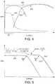
- Figure 2 shows an exemplary effect of gain on operating this type of Class AB output stage.
- the aim is to get the roll-off in Gm of the low-side output transistor (M5) to be compensated for by the rise in gain of the high side output transistor (M4).
- the standing current I Q is placed at the point where the gains overlap, and therefore each is 6dB down. With a typical CMOS output stage the I Q can be as much as 20% of the full output current.
- Reference numeral 200 denotes a plot of gain against current for the high-side (positive excursion) wide current range output stage.
- Reference numeral 202 denotes a plot of gain for the low-side (negative excursion) output stage.
- Reference numeral 204 denotes a plot of the combined gain.
- Reference numeral 206 denotes zero current on the x-axis of the plots, reference numeral 208 denotes the quiescent current on the x-axis of the plots, and reference numeral 210 denotes a maximum current on the x-axis of the plots.
- Soliman A Mahmoud, Brian Gestner et al: 51st Midwest Symposium on Circuits and Systems. MWSCAS 2008, IEEE, Piscataway, NJ, USA, 10 Aug 2008 describes a 'Low voltage current-mode digitally controlled VGA based on digitally programmable current conveyors'.
- the invention advantageously provides a Class AB amplifier with a wide operating range and minimal crossover distortion with low quiescent current.
- a class AB amplifier for receiving an input current and generating an amplified output current and having first and second output transistors connected to provide the output current, wherein if the input current is less than a threshold the first output transistor is enabled and the second output transistor is disabled, and if the input current exceeds a threshold the second output transistor is enabled.
- a first small output stage operates over a large majority of the output swings. As this stage gain begins to fall at higher currents, a second larger stage begins to take over with this second stage gain rising. Due to the statistics of the error signals the second larger stage will be called upon to deliver current infrequently. This means that any non-linearity introduced by transfer between the two gain paths does not significantly degrade the wanted signal.
- the output stage is preferably current driven. Therefore the output stage is preferably provided with a current mirror at the top and bottom.
- This output stage may be fed from other current mirrors earlier in the amplifier chain.
- a cascode stage may be placed on the input side of the mirrors.
- the function of this cascode stage is to receive the current from the previous stage and fix the headroom voltage at the previous stage. If the cascade stage is split into two, and the transistor gates are offset, then at low currents virtually all the current goes through the transistor with the highest gate voltage. However as the output current rises, the transistor with the lower gate voltage begins to conduct. Because this current is now split the gain falls. This offsets the gain at higher currents, and limits the change in gain throughout the operating range of the output stage.
- the split of current is used to provide current for the larger higher current output stage that exists in parallel with the lower current output stage.
- the invention also provides a method of controlling a class AB amplifier comprising a class AB amplifier for receiving an input current and generating an amplified output current and having first and second output transistors connected to provide the output current, wherein if the input current is less than a threshold the first output transistor is enabled and the second output transistor is disabled, and if the input current exceeds a threshold the second output transistor is enabled.
- a class AB amplifier for receiving an input current and for generating amplified output current.
- the class AB amplifier has first and second output transmitters connected to provide the output current. In accordance with a described arrangement, if the input current is less than a threshold then the first output transistor is enabled, and a second output transistor is disabled. If the input current exceeds a threshold then the second output transistor is enabled.
- the output current of a class AB amplifier is provided from either physically small or physically large output transistors in accordance with the size of the output current relative to a threshold.
- the threshold may be implementation-dependent, according to the relative size of the output transistors.
- the threshold may be compared to the input current signal.
- the threshold is set such that the physically smaller output transistors are used when the output signal is smaller, and the physically larger output transistors are used when the output is larger.
- the threshold may be a range of values, with the larger transistor switching on as the bottom of the range of values is reached.
- a modified Class AB amplifier in accordance with an embodiment is shown in Figure 3 .
- high-side (or positive) current mirror arrangement 14 is adapted to comprise of two current mirror arrangements 14a and 14b.
- Each of the current mirror arrangements 14a and 14b comprises a current mirror arrangement duplicating the current mirror arrangement 14 of Figure 1 .
- the high-side (or positive) current mirror arrangement 14a comprises transistors M3A and M4A in a current mirror arrangement
- the high-side (or positive) current mirror arrangement 14b comprises transistors M3B and M4B in a current mirror arrangement.
- the low-side (or negative) current mirror arrangement 16 is adapted to comprise of two current mirror arrangements 16a and 16b. Each of the current mirror arrangements 16a and 16b comprises a current mirror arrangement duplicating the current mirror arrangement 16 of Figure 1 .
- the low-side (or negative) current mirror arrangement 16a comprises transistors M5A and M6A in a current mirror arrangement
- the low-side (or negative) current mirror arrangement 16b comprises transistors M5B and M6B in a current mirror arrangement.
- the transistor M1 of the Figure 1 arrangement is split in the Figure 3 arrangement into two transistors M1A and M1B.
- the transistor M100 of the Figure 1 arrangement is split in the Figure 3 arrangement into two transistors M100A and M100B.
- the transistor M2 of the Figure 1 arrangement is split in the Figure 3 arrangement into two transistors M2A and M2B.
- the transistor M200 of the Figure 1 arrangement is split in the Figure 3 arrangement into two transistors M200A and M200B.
- Each of transistors M100A and M100B is connected to a different bias current, I bias+1 and I bias+2 respectively denoted by reference numerals 5A and 5B.
- the gate of transistor M1A receives a reference voltage Vref, and the voltage on the gate of transistor M1B is the reference voltage Vref plus the voltage difference between the drains of transistors M100A and M100B. In this way the threshold voltage of the transistors M1A and M1B are effectively different, so that they have different responses to the input current.
- the transistor M1A controls the current mirror pair M3A and M4A
- the transistor M1B controls the current mirror pair M3B and M4B.
- M1A, M3A and M4A only are active.
- M1B does not conduct, and hence the current mirror arrangement formed of M3B and M4B is disabled. This means that M4A can be sized just enough to handle most of the signal dynamics, which take place at low currents in the crossover region.
- M1B begins to turn on and begins to shunt current around M1A, and this enables M4B to start contributing to the output.
- M4A begins to approach saturation and the gain drops. At this point, the gain is mainly contributed by M4B.
- the larger output transistor turns on to provide the larger output current.
- Reference numeral 302 of Figure 4 denotes a plot of the gain of the small output stage of Figure 3 , provided by transistor M4A.
- Reference numeral 304 denotes a plot of the gain of the large output stage of Figure 3 , provided by transistor M4B.
- reference numeral 300 is a typical distribution of signals that will be encountered when an exemplary amplifier is used as an error amplifier in a switched envelope tracker. This means that any non-linearity contributed by the changeover to the larger stage is negligible. Because of this much reduced size of the smaller stage, the crossover quiescent current can be made much lower, and can be as low as 2% of the overall maximum output current.
- the dashed line denoted by reference numeral 306 denotes the error amplifier signal distribution (on a logarithmic scale). As denoted by reference numeral 301, the majority of activity is on the left hand side of the Figure.
- the first and second output transistors may thus be connected to a first plurality of a supply voltage.
- a third and fourth output transistor may be provided connected to a second plurality of the supply voltage. If the input current is less than a threshold the first and third output transistors may be enabled, and if the input current exceeds the threshold the second and fourth output transistors may be enabled.
- Each of transistors M200A and M200B is connected to a different bias current, I bias-1 and I bias-2 respectively denoted by reference numerals 7A and 7B.
- I bias-1 and I bias-2 respectively denoted by reference numerals 7A and 7B.
- This results in a different voltage being formed on the drain terminals of each of transistors M200A and M200, according to their respective bias currents. In turn, this provides a different voltage on the gate terminals of transistors M2A and M2B.
- the gate of transistor M2A receives the voltage Vref
- the voltage on the gate of transistor M1B is the reference voltage Vref plus the voltage difference between the drains of transistors M200A and M200B.
- the transistor M2A controls the current mirror pair M6A and M5A
- the transistor M2B controls the current mirror pair M6B and M5B.
- M2A, M6A and M5A only are active.
- M2B does not conduct, and hence the current mirror arrangement formed of M6B and M5B is disabled. This means that M5A can be sized just enough to handle most of the signal dynamics, which take place at low currents in the crossover region.
- M2B begins to turn on and begins to shunt current around M2A, and this enables M5B to start contributing to the output.
- M5A begins to approach saturation and the gain drops. At this point, the gain is mainly contributed by M5B.
- output transistors M4A and M5A are used to provide the output current which are appropriately sized for small currents.
- different output transistors M4B and M5B - appropriately sized to handle larger currents - are used.
- Some means of providing the correct gate voltage between M1A and M1B (and M2A and M2B) is preferably required, which is preferably arranged to account for changes in process and temperature. This may be achieved by the use of replica transistors for the transistors M1A and M1B, that are reduced size compared to transistor M1 in Figure 1 , but the same geometries as M1 of Figure 1 . The same applies for the transistors M2A and M2B.
- I bias+1 and I bias+2 The offset voltage necessary to generate the segmentation in current drives is obtained by providing two different bias currents in each side, which in the high side are denoted I bias+1 and I bias+2 .
- Current I bias+1 is preferably proportional to the intended crossover current, whereas I bias+2 represents the transition current to the higher current segment.
- the small stage provided by current mirror arrangements M3A/M4A and M5A/M6A has a gain plot 510 and a pole at ⁇ denoted by reference numeral 502.
- the large stage provided by current mirror arrangements M3B/M4B and M5B/M6B, has a gain plot 508 and a lower frequency pole ⁇ denoted by reference numeral 506, as the larger transistors have a lower current density.
- a cascade transistor M7 is connected between transistor M4A and the current output
- cascade transistor M8 is connected between transistor M4B and the current output
- a cascade transistor M9 is connected between transistor M5A and the current output
- a cascade transistor M10 is connected between transistor M5B and the current output.
- the gates of the transistors M7 and M8 receive a voltage from a voltage source V + 602 connected between the gates and V DD .
- the gates of the transistors M9 and M10 receive a voltage from a voltage source V - 604 connected between the gate and V ss .
Landscapes
- Engineering & Computer Science (AREA)
- Power Engineering (AREA)
- Amplifiers (AREA)
Applications Claiming Priority (2)
| Application Number | Priority Date | Filing Date | Title |
|---|---|---|---|
| GB1306621.2A GB2512916A (en) | 2013-04-11 | 2013-04-11 | Output stage for class AB amplifier |
| PCT/EP2014/057429 WO2014167114A1 (en) | 2013-04-11 | 2014-04-11 | Output stage for class ab amplifier |
Publications (2)
| Publication Number | Publication Date |
|---|---|
| EP2974009A1 EP2974009A1 (en) | 2016-01-20 |
| EP2974009B1 true EP2974009B1 (en) | 2017-06-28 |
Family
ID=48537120
Family Applications (1)
| Application Number | Title | Priority Date | Filing Date |
|---|---|---|---|
| EP14716604.5A Active EP2974009B1 (en) | 2013-04-11 | 2014-04-11 | Output stage for class ab amplifier |
Country Status (7)
| Country | Link |
|---|---|
| US (1) | US9819309B2 (cg-RX-API-DMAC7.html) |
| EP (1) | EP2974009B1 (cg-RX-API-DMAC7.html) |
| JP (1) | JP6470736B2 (cg-RX-API-DMAC7.html) |
| KR (1) | KR102234881B1 (cg-RX-API-DMAC7.html) |
| CN (1) | CN105122640B (cg-RX-API-DMAC7.html) |
| GB (1) | GB2512916A (cg-RX-API-DMAC7.html) |
| WO (1) | WO2014167114A1 (cg-RX-API-DMAC7.html) |
Families Citing this family (3)
| Publication number | Priority date | Publication date | Assignee | Title |
|---|---|---|---|---|
| CN107834986B (zh) * | 2017-11-21 | 2020-04-03 | 中国地质大学(北京) | 单级ab类运算跨导放大器及模拟电路 |
| JP7480473B2 (ja) * | 2019-03-22 | 2024-05-10 | ヤマハ株式会社 | 増幅回路 |
| DE102022109563B3 (de) * | 2022-04-20 | 2023-08-03 | It'is Foundation | Differentielle Strompufferschaltung und Stromquelle mit einer Solchen |
Family Cites Families (24)
| Publication number | Priority date | Publication date | Assignee | Title |
|---|---|---|---|---|
| JPS5718107A (en) * | 1980-07-09 | 1982-01-29 | Nippon Gakki Seizo Kk | Amplifying circuit |
| US4611180A (en) * | 1985-01-09 | 1986-09-09 | Crown International, Inc. | Grounded bridge amplifier protection through transistor thermo protection |
| US5140282A (en) * | 1990-04-27 | 1992-08-18 | U.S. Philips Corporation | Current amplifier arrangement |
| US5162753A (en) * | 1991-11-27 | 1992-11-10 | At&T Bell Laboratories | Amplifier arrangement for use as a line driver |
| JP2762333B2 (ja) * | 1992-12-22 | 1998-06-04 | ローム株式会社 | 増幅回路及び信号増幅ic |
| JP3414899B2 (ja) * | 1995-07-31 | 2003-06-09 | ローム株式会社 | オーディオ信号増幅回路およびこれを用いた音響機器 |
| JPH09186577A (ja) * | 1996-01-05 | 1997-07-15 | Kawasaki Steel Corp | 出力バッファ回路 |
| US5659266A (en) | 1996-01-16 | 1997-08-19 | National Semiconductor Corporation | Low volatage output stage with improved output drive |
| KR970063903A (ko) * | 1996-02-15 | 1997-09-12 | 모리시다 요이치 | 연산증폭기 |
| US5856749A (en) * | 1996-11-01 | 1999-01-05 | Burr-Brown Corporation | Stable output bias current circuitry and method for low-impedance CMOS output stage |
| US6188284B1 (en) * | 1999-04-23 | 2001-02-13 | Lucent Technologies Inc. | Distributed gain line driver amplifier including improved linearity |
| JP3528725B2 (ja) * | 1999-12-01 | 2004-05-24 | ヤマハ株式会社 | 電力増幅回路 |
| US6466093B1 (en) * | 2000-09-19 | 2002-10-15 | Texas Instruments Incorporated | Low voltage low thd CMOS audio (power) amplifier |
| US6501334B1 (en) * | 2000-11-13 | 2002-12-31 | Texas Instruments Incorporated | Actively biased class AB output stage with low quiescent power, high output current drive and wide output voltage swing |
| JP3535836B2 (ja) * | 2001-02-09 | 2004-06-07 | Necエレクトロニクス株式会社 | 電力増幅回路 |
| US6433637B1 (en) * | 2001-03-23 | 2002-08-13 | National Semiconductor Corporation | Single cell rail-to-rail input/output operational amplifier |
| CN1173464C (zh) * | 2001-09-25 | 2004-10-27 | 义隆电子股份有限公司 | 可低电压工作的运算放大器 |
| US6583669B1 (en) * | 2002-04-08 | 2003-06-24 | National Semiconductor Corporation | Apparatus and method for a compact class AB turn-around stage with low noise, low offset, and low power consumption |
| JP4443889B2 (ja) * | 2003-10-14 | 2010-03-31 | 旭化成エレクトロニクス株式会社 | 差動増幅器 |
| JP4789136B2 (ja) | 2005-04-07 | 2011-10-12 | ルネサスエレクトロニクス株式会社 | 演算増幅器 |
| TWI323556B (en) * | 2006-07-28 | 2010-04-11 | Realtek Semiconductor Corp | Hybrid output stage circuit and related method thereof |
| CN100578924C (zh) | 2007-07-03 | 2010-01-06 | 华为技术有限公司 | 输出级电路、功率放大电路及电信号的处理方法 |
| JP5606345B2 (ja) * | 2011-01-25 | 2014-10-15 | セイコーインスツル株式会社 | 出力回路 |
| DE102018111042A1 (de) | 2018-05-08 | 2019-11-14 | Hema Maschinen- Und Apparateschutz Gmbh | Längenvariable Schutzabdeckung |
-
2013
- 2013-04-11 GB GB1306621.2A patent/GB2512916A/en not_active Withdrawn
-
2014
- 2014-04-11 WO PCT/EP2014/057429 patent/WO2014167114A1/en not_active Ceased
- 2014-04-11 EP EP14716604.5A patent/EP2974009B1/en active Active
- 2014-04-11 KR KR1020157032094A patent/KR102234881B1/ko active Active
- 2014-04-11 JP JP2016506996A patent/JP6470736B2/ja not_active Expired - Fee Related
- 2014-04-11 US US14/775,157 patent/US9819309B2/en active Active
- 2014-04-11 CN CN201480020192.0A patent/CN105122640B/zh active Active
Non-Patent Citations (1)
| Title |
|---|
| None * |
Also Published As
| Publication number | Publication date |
|---|---|
| GB201306621D0 (en) | 2013-05-29 |
| JP6470736B2 (ja) | 2019-02-13 |
| JP2016516374A (ja) | 2016-06-02 |
| CN105122640B (zh) | 2018-06-22 |
| WO2014167114A1 (en) | 2014-10-16 |
| EP2974009A1 (en) | 2016-01-20 |
| US20160036387A1 (en) | 2016-02-04 |
| KR20150140795A (ko) | 2015-12-16 |
| GB2512916A (en) | 2014-10-15 |
| US9819309B2 (en) | 2017-11-14 |
| CN105122640A (zh) | 2015-12-02 |
| KR102234881B1 (ko) | 2021-03-31 |
Similar Documents
| Publication | Publication Date | Title |
|---|---|---|
| US9312824B2 (en) | Low noise low-dropout regulator | |
| JP5563154B2 (ja) | 広いコモンモード入力範囲を有する差動比較回路 | |
| KR101972031B1 (ko) | 동적 범위가 넓은 레일-레일 비교기를 위한 오프셋 교정 및 정밀 히스테리시스 | |
| US6891433B2 (en) | Low voltage high gain amplifier circuits | |
| US20160276993A1 (en) | Power amplifying device | |
| US9130521B2 (en) | Operational amplifier circuit | |
| EP2974009B1 (en) | Output stage for class ab amplifier | |
| US7528658B2 (en) | Threshold voltage compensation for a two stage amplifier | |
| CN114253328B (zh) | 信号处理电路 | |
| US9246439B2 (en) | Current regulated transimpedance amplifiers | |
| US9438171B2 (en) | Multiplying current conveyor for amplifier | |
| US20190280659A1 (en) | Amplifier class ab output stage | |
| US7592868B2 (en) | Rail-to-rail amplifier circuit and semiconductor device | |
| US7688145B2 (en) | Variable gain amplifying device | |
| JP6949463B2 (ja) | シングル差動変換回路 | |
| US7456692B2 (en) | Gain variable amplifier | |
| US8884695B2 (en) | Efficient supply voltage | |
| US20160036396A1 (en) | Power Amplifier, and Method of the Same | |
| TWI875248B (zh) | 放大電路 | |
| US12267052B2 (en) | Power amplifying device | |
| WO2022264716A1 (ja) | 高電圧増幅器 | |
| JP2024131165A (ja) | 増幅回路及びシステム | |
| CN120750321A (zh) | 一种自适应调整的数字输入d类音频功放系统 | |
| JP2011228887A (ja) | 増幅器 |
Legal Events
| Date | Code | Title | Description |
|---|---|---|---|
| PUAI | Public reference made under article 153(3) epc to a published international application that has entered the european phase |
Free format text: ORIGINAL CODE: 0009012 |
|
| 17P | Request for examination filed |
Effective date: 20151012 |
|
| AK | Designated contracting states |
Kind code of ref document: A1 Designated state(s): AL AT BE BG CH CY CZ DE DK EE ES FI FR GB GR HR HU IE IS IT LI LT LU LV MC MK MT NL NO PL PT RO RS SE SI SK SM TR |
|
| AX | Request for extension of the european patent |
Extension state: BA ME |
|
| DAX | Request for extension of the european patent (deleted) | ||
| REG | Reference to a national code |
Ref country code: DE Ref legal event code: R079 Ref document number: 602014011229 Country of ref document: DE Free format text: PREVIOUS MAIN CLASS: H03F0003300000 Ipc: H03F0003210000 |
|
| GRAP | Despatch of communication of intention to grant a patent |
Free format text: ORIGINAL CODE: EPIDOSNIGR1 |
|
| STAA | Information on the status of an ep patent application or granted ep patent |
Free format text: STATUS: GRANT OF PATENT IS INTENDED |
|
| RIC1 | Information provided on ipc code assigned before grant |
Ipc: H03F 3/21 20060101AFI20161123BHEP Ipc: H03F 1/02 20060101ALI20161123BHEP Ipc: H03F 3/30 20060101ALI20161123BHEP |
|
| INTG | Intention to grant announced |
Effective date: 20161222 |
|
| GRAJ | Information related to disapproval of communication of intention to grant by the applicant or resumption of examination proceedings by the epo deleted |
Free format text: ORIGINAL CODE: EPIDOSDIGR1 |
|
| STAA | Information on the status of an ep patent application or granted ep patent |
Free format text: STATUS: REQUEST FOR EXAMINATION WAS MADE |
|
| GRAR | Information related to intention to grant a patent recorded |
Free format text: ORIGINAL CODE: EPIDOSNIGR71 |
|
| GRAS | Grant fee paid |
Free format text: ORIGINAL CODE: EPIDOSNIGR3 |
|
| STAA | Information on the status of an ep patent application or granted ep patent |
Free format text: STATUS: GRANT OF PATENT IS INTENDED |
|
| GRAA | (expected) grant |
Free format text: ORIGINAL CODE: 0009210 |
|
| STAA | Information on the status of an ep patent application or granted ep patent |
Free format text: STATUS: THE PATENT HAS BEEN GRANTED |
|
| INTC | Intention to grant announced (deleted) | ||
| GRAT | Correction requested after decision to grant or after decision to maintain patent in amended form |
Free format text: ORIGINAL CODE: EPIDOSNCDEC |
|
| AK | Designated contracting states |
Kind code of ref document: B1 Designated state(s): AL AT BE BG CH CY CZ DE DK EE ES FI FR GB GR HR HU IE IS IT LI LT LU LV MC MK MT NL NO PL PT RO RS SE SI SK SM TR |
|
| INTG | Intention to grant announced |
Effective date: 20170524 |
|
| REG | Reference to a national code |
Ref country code: GB Ref legal event code: FG4D |
|
| REG | Reference to a national code |
Ref country code: CH Ref legal event code: EP |
|
| REG | Reference to a national code |
Ref country code: AT Ref legal event code: REF Ref document number: 905657 Country of ref document: AT Kind code of ref document: T Effective date: 20170715 |
|
| REG | Reference to a national code |
Ref country code: IE Ref legal event code: FG4D |
|
| REG | Reference to a national code |
Ref country code: DE Ref legal event code: R096 Ref document number: 602014011229 Country of ref document: DE |
|
| PG25 | Lapsed in a contracting state [announced via postgrant information from national office to epo] |
Ref country code: HR Free format text: LAPSE BECAUSE OF FAILURE TO SUBMIT A TRANSLATION OF THE DESCRIPTION OR TO PAY THE FEE WITHIN THE PRESCRIBED TIME-LIMIT Effective date: 20170628 Ref country code: NO Free format text: LAPSE BECAUSE OF FAILURE TO SUBMIT A TRANSLATION OF THE DESCRIPTION OR TO PAY THE FEE WITHIN THE PRESCRIBED TIME-LIMIT Effective date: 20170928 Ref country code: GR Free format text: LAPSE BECAUSE OF FAILURE TO SUBMIT A TRANSLATION OF THE DESCRIPTION OR TO PAY THE FEE WITHIN THE PRESCRIBED TIME-LIMIT Effective date: 20170929 Ref country code: FI Free format text: LAPSE BECAUSE OF FAILURE TO SUBMIT A TRANSLATION OF THE DESCRIPTION OR TO PAY THE FEE WITHIN THE PRESCRIBED TIME-LIMIT Effective date: 20170628 Ref country code: LT Free format text: LAPSE BECAUSE OF FAILURE TO SUBMIT A TRANSLATION OF THE DESCRIPTION OR TO PAY THE FEE WITHIN THE PRESCRIBED TIME-LIMIT Effective date: 20170628 |
|
| REG | Reference to a national code |
Ref country code: NL Ref legal event code: MP Effective date: 20170628 |
|
| REG | Reference to a national code |
Ref country code: LT Ref legal event code: MG4D |
|
| REG | Reference to a national code |
Ref country code: AT Ref legal event code: MK05 Ref document number: 905657 Country of ref document: AT Kind code of ref document: T Effective date: 20170628 |
|
| PG25 | Lapsed in a contracting state [announced via postgrant information from national office to epo] |
Ref country code: RS Free format text: LAPSE BECAUSE OF FAILURE TO SUBMIT A TRANSLATION OF THE DESCRIPTION OR TO PAY THE FEE WITHIN THE PRESCRIBED TIME-LIMIT Effective date: 20170628 Ref country code: LV Free format text: LAPSE BECAUSE OF FAILURE TO SUBMIT A TRANSLATION OF THE DESCRIPTION OR TO PAY THE FEE WITHIN THE PRESCRIBED TIME-LIMIT Effective date: 20170628 Ref country code: NL Free format text: LAPSE BECAUSE OF FAILURE TO SUBMIT A TRANSLATION OF THE DESCRIPTION OR TO PAY THE FEE WITHIN THE PRESCRIBED TIME-LIMIT Effective date: 20170628 Ref country code: BG Free format text: LAPSE BECAUSE OF FAILURE TO SUBMIT A TRANSLATION OF THE DESCRIPTION OR TO PAY THE FEE WITHIN THE PRESCRIBED TIME-LIMIT Effective date: 20170928 Ref country code: SE Free format text: LAPSE BECAUSE OF FAILURE TO SUBMIT A TRANSLATION OF THE DESCRIPTION OR TO PAY THE FEE WITHIN THE PRESCRIBED TIME-LIMIT Effective date: 20170628 |
|
| PG25 | Lapsed in a contracting state [announced via postgrant information from national office to epo] |
Ref country code: CZ Free format text: LAPSE BECAUSE OF FAILURE TO SUBMIT A TRANSLATION OF THE DESCRIPTION OR TO PAY THE FEE WITHIN THE PRESCRIBED TIME-LIMIT Effective date: 20170628 Ref country code: EE Free format text: LAPSE BECAUSE OF FAILURE TO SUBMIT A TRANSLATION OF THE DESCRIPTION OR TO PAY THE FEE WITHIN THE PRESCRIBED TIME-LIMIT Effective date: 20170628 Ref country code: SK Free format text: LAPSE BECAUSE OF FAILURE TO SUBMIT A TRANSLATION OF THE DESCRIPTION OR TO PAY THE FEE WITHIN THE PRESCRIBED TIME-LIMIT Effective date: 20170628 Ref country code: RO Free format text: LAPSE BECAUSE OF FAILURE TO SUBMIT A TRANSLATION OF THE DESCRIPTION OR TO PAY THE FEE WITHIN THE PRESCRIBED TIME-LIMIT Effective date: 20170628 Ref country code: AT Free format text: LAPSE BECAUSE OF FAILURE TO SUBMIT A TRANSLATION OF THE DESCRIPTION OR TO PAY THE FEE WITHIN THE PRESCRIBED TIME-LIMIT Effective date: 20170628 |
|
| PG25 | Lapsed in a contracting state [announced via postgrant information from national office to epo] |
Ref country code: ES Free format text: LAPSE BECAUSE OF FAILURE TO SUBMIT A TRANSLATION OF THE DESCRIPTION OR TO PAY THE FEE WITHIN THE PRESCRIBED TIME-LIMIT Effective date: 20170628 Ref country code: IS Free format text: LAPSE BECAUSE OF FAILURE TO SUBMIT A TRANSLATION OF THE DESCRIPTION OR TO PAY THE FEE WITHIN THE PRESCRIBED TIME-LIMIT Effective date: 20171028 Ref country code: SM Free format text: LAPSE BECAUSE OF FAILURE TO SUBMIT A TRANSLATION OF THE DESCRIPTION OR TO PAY THE FEE WITHIN THE PRESCRIBED TIME-LIMIT Effective date: 20170628 Ref country code: IT Free format text: LAPSE BECAUSE OF FAILURE TO SUBMIT A TRANSLATION OF THE DESCRIPTION OR TO PAY THE FEE WITHIN THE PRESCRIBED TIME-LIMIT Effective date: 20170628 Ref country code: PL Free format text: LAPSE BECAUSE OF FAILURE TO SUBMIT A TRANSLATION OF THE DESCRIPTION OR TO PAY THE FEE WITHIN THE PRESCRIBED TIME-LIMIT Effective date: 20170628 |
|
| REG | Reference to a national code |
Ref country code: FR Ref legal event code: PLFP Year of fee payment: 5 |
|
| REG | Reference to a national code |
Ref country code: DE Ref legal event code: R097 Ref document number: 602014011229 Country of ref document: DE |
|
| PG25 | Lapsed in a contracting state [announced via postgrant information from national office to epo] |
Ref country code: DK Free format text: LAPSE BECAUSE OF FAILURE TO SUBMIT A TRANSLATION OF THE DESCRIPTION OR TO PAY THE FEE WITHIN THE PRESCRIBED TIME-LIMIT Effective date: 20170628 |
|
| PLBE | No opposition filed within time limit |
Free format text: ORIGINAL CODE: 0009261 |
|
| STAA | Information on the status of an ep patent application or granted ep patent |
Free format text: STATUS: NO OPPOSITION FILED WITHIN TIME LIMIT |
|
| 26N | No opposition filed |
Effective date: 20180329 |
|
| PG25 | Lapsed in a contracting state [announced via postgrant information from national office to epo] |
Ref country code: SI Free format text: LAPSE BECAUSE OF FAILURE TO SUBMIT A TRANSLATION OF THE DESCRIPTION OR TO PAY THE FEE WITHIN THE PRESCRIBED TIME-LIMIT Effective date: 20170628 |
|
| PG25 | Lapsed in a contracting state [announced via postgrant information from national office to epo] |
Ref country code: MC Free format text: LAPSE BECAUSE OF FAILURE TO SUBMIT A TRANSLATION OF THE DESCRIPTION OR TO PAY THE FEE WITHIN THE PRESCRIBED TIME-LIMIT Effective date: 20170628 |
|
| REG | Reference to a national code |
Ref country code: CH Ref legal event code: PL |
|
| REG | Reference to a national code |
Ref country code: BE Ref legal event code: MM Effective date: 20180430 |
|
| REG | Reference to a national code |
Ref country code: IE Ref legal event code: MM4A |
|
| PG25 | Lapsed in a contracting state [announced via postgrant information from national office to epo] |
Ref country code: LU Free format text: LAPSE BECAUSE OF NON-PAYMENT OF DUE FEES Effective date: 20180411 |
|
| PG25 | Lapsed in a contracting state [announced via postgrant information from national office to epo] |
Ref country code: CH Free format text: LAPSE BECAUSE OF NON-PAYMENT OF DUE FEES Effective date: 20180430 Ref country code: BE Free format text: LAPSE BECAUSE OF NON-PAYMENT OF DUE FEES Effective date: 20180430 Ref country code: LI Free format text: LAPSE BECAUSE OF NON-PAYMENT OF DUE FEES Effective date: 20180430 |
|
| PG25 | Lapsed in a contracting state [announced via postgrant information from national office to epo] |
Ref country code: IE Free format text: LAPSE BECAUSE OF NON-PAYMENT OF DUE FEES Effective date: 20180411 |
|
| PG25 | Lapsed in a contracting state [announced via postgrant information from national office to epo] |
Ref country code: MT Free format text: LAPSE BECAUSE OF NON-PAYMENT OF DUE FEES Effective date: 20180411 |
|
| PG25 | Lapsed in a contracting state [announced via postgrant information from national office to epo] |
Ref country code: TR Free format text: LAPSE BECAUSE OF FAILURE TO SUBMIT A TRANSLATION OF THE DESCRIPTION OR TO PAY THE FEE WITHIN THE PRESCRIBED TIME-LIMIT Effective date: 20170628 |
|
| PG25 | Lapsed in a contracting state [announced via postgrant information from national office to epo] |
Ref country code: PT Free format text: LAPSE BECAUSE OF FAILURE TO SUBMIT A TRANSLATION OF THE DESCRIPTION OR TO PAY THE FEE WITHIN THE PRESCRIBED TIME-LIMIT Effective date: 20170628 |
|
| PG25 | Lapsed in a contracting state [announced via postgrant information from national office to epo] |
Ref country code: MK Free format text: LAPSE BECAUSE OF NON-PAYMENT OF DUE FEES Effective date: 20170628 Ref country code: HU Free format text: LAPSE BECAUSE OF FAILURE TO SUBMIT A TRANSLATION OF THE DESCRIPTION OR TO PAY THE FEE WITHIN THE PRESCRIBED TIME-LIMIT; INVALID AB INITIO Effective date: 20140411 Ref country code: CY Free format text: LAPSE BECAUSE OF FAILURE TO SUBMIT A TRANSLATION OF THE DESCRIPTION OR TO PAY THE FEE WITHIN THE PRESCRIBED TIME-LIMIT Effective date: 20170628 |
|
| PG25 | Lapsed in a contracting state [announced via postgrant information from national office to epo] |
Ref country code: AL Free format text: LAPSE BECAUSE OF FAILURE TO SUBMIT A TRANSLATION OF THE DESCRIPTION OR TO PAY THE FEE WITHIN THE PRESCRIBED TIME-LIMIT Effective date: 20170628 |
|
| REG | Reference to a national code |
Ref country code: DE Ref legal event code: R082 Ref document number: 602014011229 Country of ref document: DE Representative=s name: MAUCHER JENKINS PATENTANWAELTE & RECHTSANWAELT, DE |
|
| PGFP | Annual fee paid to national office [announced via postgrant information from national office to epo] |
Ref country code: DE Payment date: 20250317 Year of fee payment: 12 |
|
| PGFP | Annual fee paid to national office [announced via postgrant information from national office to epo] |
Ref country code: GB Payment date: 20260320 Year of fee payment: 13 |
|
| PGFP | Annual fee paid to national office [announced via postgrant information from national office to epo] |
Ref country code: FR Payment date: 20260317 Year of fee payment: 13 |