EP2964007B1 - Communication system and electronic component mounting device - Google Patents
Communication system and electronic component mounting device Download PDFInfo
- Publication number
- EP2964007B1 EP2964007B1 EP13876183.8A EP13876183A EP2964007B1 EP 2964007 B1 EP2964007 B1 EP 2964007B1 EP 13876183 A EP13876183 A EP 13876183A EP 2964007 B1 EP2964007 B1 EP 2964007B1
- Authority
- EP
- European Patent Office
- Prior art keywords
- communication
- electronic component
- data
- mounting
- movable portion
- Prior art date
- Legal status (The legal status is an assumption and is not a legal conclusion. Google has not performed a legal analysis and makes no representation as to the accuracy of the status listed.)
- Active
Links
Images


Classifications
-
- H—ELECTRICITY
- H05—ELECTRIC TECHNIQUES NOT OTHERWISE PROVIDED FOR
- H05K—PRINTED CIRCUITS; CASINGS OR CONSTRUCTIONAL DETAILS OF ELECTRIC APPARATUS; MANUFACTURE OF ASSEMBLAGES OF ELECTRICAL COMPONENTS
- H05K13/00—Apparatus or processes specially adapted for manufacturing or adjusting assemblages of electric components
- H05K13/08—Monitoring manufacture of assemblages
- H05K13/081—Integration of optical monitoring devices in assembly lines; Processes using optical monitoring devices specially adapted for controlling devices or machines in assembly lines
- H05K13/0812—Integration of optical monitoring devices in assembly lines; Processes using optical monitoring devices specially adapted for controlling devices or machines in assembly lines the monitoring devices being integrated in the mounting machine, e.g. for monitoring components, leads, component placement
Definitions
- the present invention relates to a communication system that transmits processing results of an imaging device having an image processing function and an electronic component mounting device using the communication system.
- Automatic machines such as electronic component mounting devices or industrial robots, which operate in various manufacturing lines, perform, for example, work for mounting workpieces, such as electronic components, which are held by movable portions, such as mounting heads or arms, on circuit boards.
- the automatic machine performs mounting work on the basis of a control program, and adjusts positions when the actual positions of the electronic component of the movable portion and the circuit board deviate from desired relative positions set in the control program.
- an automatic machine including an imaging device that images an electronic component to be held and performs image processing and is provided on the movable portion (PTL 1 and the like).
- the imaging device performs image processing for detecting the amount of the deviation of the orientation and the position of an electronic component and the like from obtained image data.
- the imaging device transmits the processing results to a control unit through a network.
- the control unit drives the movable portion on the basis of the processing results received from the imaging device, to adjust the orientation of the electronic component through rotation and the like of the electronic component.
- this kind of automatic machine transmits the data of an actual image, which is taken by the imaging device, as it is and displays the data on a monitor.
- the amount of data of an actual image, which is not subjected to image processing becomes larger than the amount of data of the processing results, such as the amount of the deviation of the orientation and the position of the electronic component obtained from image processing. For this reason, since the transmission time of the actual image becomes longer than the transmission time of the processing results when the actual image is transmitted as it is, a connection port for the network is used for an extended period of time.
- two virtual interfaces (command interfaces CF1 and CF2 in PTL 1) are realized at one physical connection port connected to a network (Ethernet (registered trademark) in PTL 1), and the interfaces are separately used for image processing result data and actual image data.
- a communication system according to the preamble of independent claim 1 is known from PTL 2.
- Another example is known from PTL3.
- the invention has been made in consideration of the above-mentioned problem, and an object of the invention is to provide a communication system in which transmission efficiency is improved by the optimization of a communication line according to the amount of data to be transmitted and manufacturing costs are consequently reduced, and an electronic component mounting device using the communication system.
- a communication system includes a movable portion that holds and moves a workpiece, an imaging device that is integrally provided on the movable portion and performs image processing for extracting necessary information from image data of a state in which the movable portion holds the workpiece, a control unit that drives the movable portion on the basis of processing result data of the image processing performed by the imaging device, first communication means for transmitting the processing result data to the control unit from the imaging device, and second communication means other than the first communication means.
- the control unit transmits the image data from the imaging device on the basis of the processing result data by the second communication means.
- an electronic component mounting device transmits data related with work for mounting an electronic component, which is held as the workpiece by the movable portion, on a circuit board by the communication system according to the technique disclosed in this application.
- the communication system includes a movable portion that holds and moves a workpiece, an imaging device that is integrally provided on the movable portion and performs image processing for extracting necessary information from image data of a state in which the movable portion holds the workpiece, a control unit that drives the movable portion on the basis of processing result data of the image processing performed by the imaging device, first communication means for transmitting the processing result data to the control unit from the imaging device, and second communication means other than the first communication means.
- the control unit transmits the image data from the imaging device on the basis of the processing result data by the second communication means.
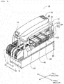
- FIG. 1 is a perspective view of a mounting apparatus 10 from which a part of exterior components are removed.
- the mounting device 10 is a mounting apparatus that includes one system base 12 and two electronic component mounting machines (hereinafter, abbreviated as “mounting machines” in some cases) 16 arranged so as to line up on the system base 12 and mounts an electronic component P (see Fig. 3 ) on a circuit board.
- a direction in which the mounting machines 16 are arranged side by side as shown in Fig. 1 is referred to as an X-axis direction
- a direction that is parallel to a horizontal direction so as to be orthogonal to the X-axis direction is referred to as a Y-axis direction
- a direction that is orthogonal to the X-axis direction and the Y-axis direction is referred to as a vertical direction.
- the mounting machine 16 includes a mounting machine body 24 that includes a frame portion 20 and a beam portion 22 mounted on the frame portion 20, a conveyance device 26 that conveys a circuit board in the X-axis direction and lifts up and clamps the circuit board at a set position, a mounting head 28 that performs mounting work on the circuit board fixed by the conveyance device 26, a moving device 30 that is provided on the beam portion 22 and moves the mounting head 28 in the X-axis direction and the Y-axis direction, and an electronic component supply device (hereinafter, abbreviated as a "supply device” in some cases) 32 that is connected to a front portion of the frame portion 20 and supplies electronic components P.
- a supply device an electronic component supply device
- the mounting machine 16 includes an operation panel 18 that is provided on the outside of the beam portion 22.
- the operation panel 18 is a touch screen-type display device, and can receive operations, such as the starting and stopping, of work for mounting the electronic component P and can display information about the work.
- the conveyance device 26 is a so-called double-conveyor type device that includes two conveyor units 40 and 42.
- the respective conveyor units 40 and 42 are provided substantially in the middle of the frame portion 20 in the Y-axis direction, and are arranged side by side in the Y-axis direction. Further, the conveyor units 40 and 42 are fixed so that the conveying directions of the conveyor units 40 and 42 are parallel to the X-axis direction.
- Each of the conveyor units 40 and 42 conveys and fixes a circuit board.
- the moving device 30 is a so-called XY robot-type moving device, and drives an electromagnetic motor 52 (see Fig.
- the slider 50 which is built in a slider 50, to allow the slider 50 to slide in the Y-axis direction along a guide rail (not shown) that is held on the beam portion 22.
- the slider 50 is provided with a guide rail (not shown) parallel to the X-axis direction, and the mounting head 28 is mounted on the guide rail through a guide block 90 (see Fig. 2 ).
- an electromagnetic motor 54 (see Fig. 5 ), which is built in the mounting head 28, is driven, the mounting head 28 is moved in the X-axis direction along the guide rail of the slider 50.
- the moving device 30 can move the mounting head 28 to an arbitrary position on the frame portion 20 by driving the two electromagnetic motors 52 and 54.
- the electromagnetic motors 52 and 54 are, for example, linear motors.
- Fig. 2 is a perspective view of the mounting head 28 that is separated from the guide rail of the slider 50, and the guide block 90 is provided on the side surface of the mounting head 28 facing the slider 50.
- the mounting head 28 includes multiple sets (in this embodiment, 12 sets) of a suction nozzle 80, which sucks the electronic component P (see Fig. 3 ), and a mounting unit 82 that holds the suction nozzle 80 at a distal end portion thereof.
- Each of the suction nozzles 80 communicates with a positive/negative pressure supply device (not shown) through a negative-pressure air passage and a positive-pressure air passage, and is adapted to suck and hold the electronic component P with negative pressure and release the held electronic component P by the supply of slightly positive pressure.
- the mounting unit 82 is formed substantially in the shape of a bar, and is held so that an axial direction of the mounting unit 82 is parallel to the vertical direction of the mounting device 10.
- the mounting units 82 are provided on an outer peripheral portion of a substantially cylindrical unit holding body 86 at regular intervals.
- the unit holding body 86 is rotatably supported by a head body 88 of the mounting head 28, and is intermittently rotated together with the mounting units 82 by a holding body rotating device (not shown) .
- the mounting units 82 are adapted to move in the vertical direction with the intermittent rotation of the unit holding body 86.
- each mounting unit 82 moves to the lowermost end at a stop position (hereinafter, referred to as a "mounting station") where the mounting unit is farthest from the head body 88.
- the suction nozzle 80 sucks and holds the electronic component P at the mounting station or mounts the held electronic component P on a circuit board.
- each mounting unit 82 moves to the uppermost end at a stop position (hereinafter, referred to as an "imaging station") where the mounting unit is closest to the head body 88 and at four stop positions of which two stop positions are present on each of both sides of the imaging station in a rotational direction. That is, the mounting units 82 present at a total of five stop positions, which include the imaging station and four stop positions present on both sides of the imaging station, move to the uppermost end.
- the mounting head 28 includes unit rotating devices (not shown) that rotate the mounting units 82 about the axes of the mounting units 82, respectively, and is adapted to be capable of changing the holding postures of the electronic components P that are sucked and held by the respective mounting units 82.
- the mounting head 28 includes a unit lifting and lowering device 89 that individually lifts and lowers the mounting units 82, and moves the mounting unit 82 to an arbitrary position in the vertical direction.
- a lower end portion of the head body 88 extends downward further than a distal end portion of the suction nozzle 80 that is positioned at the mounting station.
- a part camera 96 is provided at a portion of the head body 88 that faces the distal end portion of the suction nozzle 80. The part camera 96 images the electronic component P that is held by the suction nozzle 80 positioned at the imaging station. Further, the extending distal end portion of the head body 88 is formed so as to be bent toward the suction nozzle 80.
- a mark camera 98 (see Fig. 5 ) is provided at the bent portion of the head body 88. The mark camera 98 is fixed so as to face the lower side, and images a reference position mark of a circuit board, an ID mark used to identify a circuit board, the mounting state of the electronic component P, or the like.
- Fig. 3 is a partial enlarged view of the mounting head 28 that holds the electronic component P.
- a cylindrical reflector 86A which can reflect light
- a box-shaped bracket 91 is fixed to a portion of the head body 88 where the part camera 96 faces the suction nozzle 80.
- a light source (not shown), such as a LED, which emits light toward the reflector 86A, is provided in the bracket 91. Light, which is emitted from the light source, is reflected by the reflector 86A and is incident on the bracket 91 from an incident portion 91A.
- the reflector 86A, the electronic component P sucked by the suction nozzle 80, and the incident portion 91A line up on a virtual straight line 92.
- Two prisms 94 are provided in the bracket 91. As shown in Fig. 3 by an arrow, light reflected by the reflector 86A passes through an outer peripheral edge of the electronic component P and the incident portion 91A, is reflected by the prisms 94, and is incident on the part camera 96.
- the part camera 96 acquires the two-dimensional image of the electronic component P that is sucked by the suction nozzle 80.
- the bracket 91 is provided with a shield plate preventing light from being directly emitted to the electronic component P from the light source.
- the supply device 32 is a feeder-type supply device, and includes a plurality of tape feeders 74 and feeder bodies 77 (see Fig. 4 ).
- the plurality of tape feeders 74 store tape-shaped components 70 (see Fig. 4 ), which are obtained by taping electronic components P, while the tape-shaped components 70 are wound on reels 72.
- the feeder bodies 77 feed the tape-shaped components 70 that are stored in the plurality of tape feeders 74.
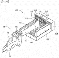
- the supply device 32 sequentially supplies the electronic components P to a supply position from the tape-shaped component 70. In a perspective view of Fig. 4 , a part of exterior components are removed from the tape feeder 74. As shown in Fig.
- each tape feeder 74 includes a reel holder 76 that holds the reel 72 on which the tape-shaped component 70 is wound, and the feeder body 77 that allows the tape-shaped component 70 unwound from the reel 72 to extend on an upper end face thereof.
- a sprocket (not shown) built in the feeder body 77 is rotated, the tape-shaped component 70 is fed on the upper end face of the feeder body 77 in a direction where the tape-shaped component 70 becomes distant from the reel 72.
- the electronic components P are sequentially released from the tape-shaped component 70 at the supply position, which is present at the distal end portion of the feeder body 77, by a peeling device (not illustrated), and are taken out by the suction nozzles 80.
- the tape feeder 74 is detachably mounted on a feeder support table 100 that is provided at the front end portion of the frame portion 20 (see Fig. 1 ).
- the feeder support table 100 includes a slot portion 102 that is formed on the upper surface of the frame portion 20 and a connecting portion 106 that stands at the rear end portion of the slot portion 102 (close to the conveyance device 26).
- a plurality of slots 108 are formed on the slot portion 102 in the Y-axis direction.
- a lower edge portion of the feeder body 77 slides on each of the plurality of slots 108 and the tape feeder 74 is connected to the connecting portion 106.
- a connector 114 and a pair of positioning pins 116 which are positioned on both sides of the connector 114 in the vertical direction, are provided on the surface of the feeder body 77 facing the connecting portion 106. Meanwhile, a connector 112 to which the connector 114 is connected and a pair of fitting holes 118 into which the positioning pins 116 are fitted are formed at the connecting portion 106 so as to correspond to each of the slots 108. Power is supplied to the tape feeder 74 from the feeder support table 100 through the connectors 112 and 114 connected to each other, and the tape feeder 74 transmits necessary control signals (a component request signal, a component-supply-completion signal, and the like) and management information such as the IDs of each tape feeder 74.
- necessary control signals a component request signal, a component-supply-completion signal, and the like
- a discard box 122 into which the electronic components P are discarded is mounted on the feeder support table 100.
- the discard box 122 is used to collect electronic components P that are not mounted on a circuit board due to the reason that electronic components P are not sucked in a normal posture by the suction nozzles 80, or the like. Similar to the tape feeder 74, the discard box 122 is provided with a connector and positioning pins (not shown) that are connected to the connecting portion 106.
- the discard box 122 transmits management information, such as the ID used to identify the discard box 122, through the connector 112. Meanwhile, the discard box 122 may be provided for each type of electronic components P.
- the mounting device 10 is adapted to use optical wireless communication for the transmission of data between a controller 201 and a movable portion (the slider 50 and the mounting head 28) of the mounting device 10.
- Fig. 5 shows the schematic configuration of the mounting device 10, and the respective devices of the mounting apparatus 10 are appropriately omitted in Fig. 5 .
- the configuration of the communication system shown in Fig. 5 is exemplary, and is appropriately modified according to the types and the number of the devices included in the mounting device 10.
- the communication system of this application is a system that can be applied to automatic machines and the like operating in various manufacturing lines other than the electronic component mounting device exemplified as the mounting device 10.
- the mounting device 10 includes the controller 201 mainly configured by a computer which includes a CPU and the like, an optical wireless communication I/F (hereinafter, referred to as an "optical wireless I/F") 211, a drive control board 212, and a near field communication I/F (hereinafter, referred to as a "near field communication I/F) 213 that are built in the mounting machine body 24.
- the optical wireless I/F 211 processes the transmission of data to/from the respective cameras 96 and 98 of the mounting head 28.
- the drive control board 212 is a board that controls operation instructions to the electromagnetic motor 52 of the slider 50 and the electromagnetic motor 54 of the mounting head 28 and the input/output of information and the like fed back from the electromagnetic motors 52 and 54 in real time.
- the drive control board 212 controls drive circuits 215, which are connected to the electromagnetic motors 52 and 54 by cables, to drive the respective motors 52 and 54.
- the near field communication I/F 213 controls the start and the like of data transmission of a near field communication section (hereinafter, referred to as a "communication section") 217 that is connected to the near field communication I/F 213 by a cable.
- the optical wireless I/F 211 is connected to an optical wireless device 221 that is built in the mounting machine body 24 .
- the slider 50 is provided with an optical wireless device 222 that faces the optical wireless device 221.
- the optical wireless device 222 is fixed to the slider 50 so that, for example, an optical axis of the optical wireless device 222 parallel to the Y-axis direction corresponds to that of the optical wireless device 221 of the mounting machine body 24.
- Input/output data of the optical wireless I/F 211 is transmitted to the optical wireless devices 221 and 222 by optical wireless communication using, for example, an LED and the like.
- data is transmitted and received as multiplexed data, for example, time division multiplex (TDM) frame data.
- TDM time division multiplex
- the optical wireless device 222 is connected to an optical wireless device 224 that is built in the slider 50.
- the mounting head 28 is provided with an optical wireless device 225 that faces the optical wireless device 224.
- the optical wireless device 225 is fixed to the mounting head 28 so that an optical axis of the optical wireless device 225 parallel to the X-axis direction corresponds to that of the optical wireless device 224 of the slider 50.
- Input/output data of the optical wireless I/F 211 is transmitted to the optical wireless devices 224 and 225 by optical wireless communication.
- the part camera 96 of the mounting head 28 includes an imaging unit 231, an image processing section 232, an I/F circuit 233, a memory unit 235, and a near field communication section (hereinafter, referred to as a "communication section") 237.
- the imaging unit 231 is an imaging element, such as a CMOS sensor or a CCD sensor.
- the imaging unit 231 outputs obtained image data to the image processing section 232.
- the image processing section 232 performs various kinds of image processing for extracting necessary information from the image data that is input from the imaging unit 231.
- the image processing section 232 controls the I/F circuit 233 and outputs processing result data to the optical wireless device 225.
- the optical wireless device 225 transmits processing results to the optical wireless device 221 provided in the apparatus body through the optical wireless devices 224 and 222 of the slider 50.
- the image processing section 232 performs edge detection processing, gamma correction, contour emphasis, and the like as various kinds of image processing for extracting necessary information.
- the image processing section 232 calculates, for example, a value, which is used to correct the amount of a positional deviation of an electronic component P to be sucked by the suction nozzle 80, from edge detection processing results.
- the mark camera 98 has an image processing function to extract necessary information and detects the reference position mark of a circuit board to calculate a value that is used to correct the amount of a positional deviation of the circuit board.
- the part camera 96 transmits a position correction value to the controller 201 through the optical wireless device 225.
- the controller 201 moves the mounting head 28 to a position above the circuit board conveyed by the conveyance device 26 (see Fig. 1 ), and corrects an error between holding positions of the circuit board and the electronic component P on the basis of the position correction values received from the respective cameras 96 and 98.
- the controller 201 mounts the electronic component P on the circuit board after correcting the holding position of the electronic component by moving or rotating the suction nozzle 80 according to the error of the holding position. Meanwhile, although not shown in Fig. 5 , the controller 201 performs the correction of the holding position of the above-mentioned suction nozzle 80 by controlling the driving of servo motors or the like of the mounting unit 82 and the unit lifting and lowering device 89 (see Fig. 2 ) of the mounting head 28.
- the control data is transmitted through optical wireless communication (the optical wireless device 221 and the like).
- the image processing section 232 compares, for example, the edge detection processing results with preset dimensions of each electronic component P and determines whether or not the electronic component P is sucked normally by the suction nozzle 80.
- a reason why the electronic component P is not held normally by the suction nozzle 80 includes various cases, such as a case in which the orientation of the electronic component P held by the suction nozzle 80 is wrong and a case in which the electronic component P is not sucked by the suction nozzle 80. For this reason, a user of the mounting device 10 needs to confirm an actual image that is taken when the electronic component is sucked and held abnormally.
- the amount of actual image data of the distal end portion or the like of the suction nozzle 80 becomes larger than the amount of processing result data such as position correction values transmitted when the electronic component is sucked and held normally. That is, in order to transmit actual image data through an optical wireless communication line that is normally used, it is necessary to increase the data transmission speed of the communication line according to the transmission of a large amount of data that temporarily occurs in a working process such as a case in which the electronic component is sucked and held abnormally. Accordingly, in the mounting device 10 according to this embodiment, actual image data is transmitted between each of the cameras 96 and 98 and the apparatus body through near field communication that is separate from optical wireless communication when abnormality, such as a case in which the electronic component P is not held normally, is detected.
- the image processing section 232 performs image processing and performs processing for storing actual image data, which is input from the imaging unit 231, in the memory unit 235.
- the controller 201 receives processing result data representing that the electronic component P is not held normally from the image processing section 232, the controller 201 moves the mounting head 28 to a position above the discard box 122 (see Fig. 4 ) and performs processing for releasing the electronic component P from the suction nozzle 80 to discard the electronic component P.
- the mounting head 28 transmits the actual image data, which are stored in the memory unit 235, to the communication section 217 provided in the apparatus body from the communication section 237 through near field communication.
- the near field communication between the communication sections 217 and 237 is performed using a communication technique such as TransferJET (registered trademark).
- Communication speed between the communication sections 217 and 237 is, for example, 350 Mbps and is higher than the speed of optical wireless communication.
- wireless devices the optical wireless devices 221, 222, 224, and 225 of which communication speed is lower than the communication speed of the near field communication sections 217 and 237 can be used for optical wireless communication that normally transmits processing result data (position correction values and the like) of the respective cameras 96 and 98. Accordingly, since the transmission of a large amount of data, which temporarily occurs in a working process when the electronic component is sucked and held abnormally, is performed through a separate line, the data transmission speed of a normal communication line can be reduced.
- the communication section 217 provided in the apparatus body is provided on the connecting portion 106 of the feeder support table 100.
- the communication section 217 is provided at a position facing the communication section 237 of the part camera 96 when the controller 201 moves the mounting head 28 to the discard box 122 to discard the electronic component P.
- the mounting head 28 approaches the connecting portion 106 and the discard box 122 with a distance of, for example, about several centimeters therebetween.
- the actual image data which is received from the communication section 237 through near field communication by the communication section 217, is input to the controller 201 from the near field communication I/F 213. Accordingly, the controller 201 can process an operation for discarding the electronic component P in parallel with processing for receiving the actual image data.
- the controller 201 performs mounting work on the basis of a control program and the like. However, since the controller 201 is adapted to simultaneously perform existing processing for discarding the electronic component P and the transmission of the actual image data, the control program is easily changed. Furthermore, since time required to transmit actual image data does not need to be separately reserved, production efficiency is barely affected. That is, the data transmission speed of a normal communication line is also reduced without the reduction of production efficiency even when image data is transmitted. Moreover, since the controller 201 can transmit data through optical wireless communication even when the controller 201 performs near field communication, it is possible to remove the influence of the transmission of actual image data on the transmission of normal processing result data.
- the controller 201 transmits the received actual image data to a control device (not shown) that performs the centralized management of, for example, a plurality of mounting machines 16; and processing for storing the actual image data in an external storage device is performed by the control device.
- the controller 201 performs processing for transmitting other information (for example, time information, the type of the electronic component P, ID of the discard box 122, identification information of the suction nozzle 80, ID of the circuit board, and the like) together when the actual image data is stored.
- other information for example, time information, the type of the electronic component P, ID of the discard box 122, identification information of the suction nozzle 80, ID of the circuit board, and the like
- the controller 201 may be set to transmit the actual image data, which is received through, for example, a network, to a vendor and the like. Accordingly, a user can quickly and accurately cope with poor mounting with reference to an expert's determination.
- the communication sections 217 and 237 can perform bidirectional near field communication.
- the controller 201 transmits setting data related with the image processing of the part camera 96, which corresponds to a changed electronic component P, by the communication sections 217 and 237.
- the setting data is setting values of the size and the like of an area, which corresponds to, for example, the shape or size of the electronic component P and is to be subjected to image processing.
- the amount of the setting data may be larger than the amount of processing result data, such as position correction values output from the image processing section 232.
- the controller 201 moves the mounting head 28 to the position of the communication section 217 of the connecting portion 106 (see Fig. 4 ) according to processing or the like for changing the tape feeder 74 to be driven and transmits the setting data to the communication section 237. Accordingly, it is not necessary to increase the data transmission speed of a normal communication line according to the transmission of a large amount of data that temporarily occurs in a working process such as a case in which the electronic component P is changed. Meanwhile, the controller 201 may transmit the actual image data from the mounting head 28 when transmitting the setting data through the near field communication.
- the mounting device 10 includes the part camera 96 and the mark camera 98 that are provided on the mounting head 28.
- the part camera 96 images the electronic component P sucked by the suction nozzle 80
- the mark camera 98 images the reference position mark of the circuit board or the like.
- Each of the cameras 96 and 98 has an image processing function to process the taken image data.
- the mounting device 10 includes two types of communication means for transmitting the data of the respective cameras 96 and 98.
- Each of the cameras 96 and 98 transmits the processing result data of whether or not the electronic component P is sucked normally by the suction nozzle 80 to the controller 201 as the result of image processing through the optical wireless communication that is performed through the optical wireless devices 221, 222, 224, and 225.
- the controller 201 performs control for transmitting the actual image data to each of the cameras 96 and 98.
- Each of the cameras 96 and 98 transmits the actual image data to the controller 201 through the near field communication that is performed through the communication sections 217 and 237.
- the amount of processing result data of image processing, which are normally transmitted, is smaller than the amount of actual image data that is necessary when the electronic component is sucked and held abnormally.
- wireless devices the optical wireless device 221, and the like
- the data transmission speed of a normal communication line can be reduced. That is, it is possible to improve transmission efficiency by optimizing the communication line according to the amount of data to be transmitted. Consequently, since low-speed and inexpensive wireless communication devices are used, it is possible to reduce manufacturing costs.
- optical wireless communication has been exemplified as a normal communication means in the above-mentioned embodiment.
- this application is not limited thereto; and wireless communication using various electromagnetic waves other than infrared light, visible light, and the like or wired communication (for example, communication standards based on RS485, and the like) may be applied.
- the communication speed of wired communication is lower than the speed of near field communication (for example, about 10 Mbps). Accordingly, it is possible to improve transmission efficiency and to reduce manufacturing costs by optimizing the communication line according to the amount of data to be transmitted.
- the structure of the sheath or the like of the cable is restricted when the impedance of a communication cable used for wired communication is reduced or the impedance of the communication cable is adjusted, the elasticity of a cable capable of being used for general high-speed communication is low.
- a cable having low elasticity is used as a cable, which connects the apparatus body of the above-mentioned mounting device 10 to the movable mounting head 28, in order to increase data transmission speed, the degree of freedom of wiring in the mounting apparatus 10 is restricted and the possibility of the breaking of an internal signal line is increased.
- the data transmission speed of a normal communication line is reduced through the optimization of the communication line according to the amount of data to be transmitted.
- the guide rail of the slider 50 which is parallel to the X-axis direction
- a flat-plate electrode which faces the guide block 90 of the mounting head 28, may be provided to transmit data by the change of capacitance.
- the near field communication of the above-mentioned embodiment is not limited to TransferJET (registered trademark); and communication means suitable for other communications standards, such as standards of infrared light communication (Giga-IR), Bluetooth (registered trademark), standards (IEEE802.11) of wireless LAN, Zigbee (registered trademark), and the like may be used.
- the communication between the communication sections 217 and 237 is not limited to near field communication, and other wireless communication systems or wired communication may be used. Further, the communication between the communication sections 217 and 237 may be communication of which speed is lower than the speed of the optical wireless communication (the communication between the optical wireless devices 221, 222, 224, and 225).
- the communication sections 217 and 237 as second communication means may be formed as separate lines other than the optical wireless communication (first communication means) that transmits the processing result data of image processing. Even in this configuration, transmission efficiency is improved through the optimization of the communication line according to the amount of data to be transmitted.
- the electronic component mounting device 10 which mounts an electronic component P on a circuit board, has been described in the above-mentioned embodiment.
- the invention is not limited thereto and can be applied to automatic machines and the like operating in various other manufacturing lines.
- the invention may be applied to an automatic machine that assembles a secondary cell (a solar cell, a fuel cell, or the like) and the like.
- an assembly component which is held by a movable portion, such as a mounting head or an arm, is used as a workpiece that is imaged by the imaging unit 231, and the invention may be applied to a communication system that transmits image data thereof and processing result data.
- the automatic machine is not limited to a machine that performs mounting or assembling, but the invention may be applied to, for example, a machine tool that performs cutting and the like.
- a workpiece or the like, which is to be cut may be used as an object to be imaged.
- the configuration of the mounting device 10 according to the embodiment is exemplary and may be appropriately modified.
- the positions of the communication sections 217 and 237 of the mounting device 10 and a timing in which the near field communication is performed are exemplary, and may be appropriately changed.
- each of the mounting machines 16 may include multiple sets of the mounting head 28 and the moving device 30.
- the electronic component mounting device 10 corresponds to an example of an electronic component mounting device
- the mounting head 28 corresponds to an example of a movable portion
- the part camera 96 and the mark camera 98 correspond to an example of an imaging device
- the discard box 122 and the connecting portion 106 correspond to an example of a storage unit
- the controller 201 corresponds to an example of a control unit
- the optical wireless devices 221, 222, 224, and 225 correspond to an example of first communication means
- the communication sections 217 and 237 correspond to an example of second communication means for performing near field communication
- the communication section 217 corresponds to an example of a receiving unit
- the electronic component P corresponds to an example of a workpiece and an electronic component
- the position correction value corresponds to an example of processing result data.
Description
- The present invention relates to a communication system that transmits processing results of an imaging device having an image processing function and an electronic component mounting device using the communication system.
- Automatic machines, such as electronic component mounting devices or industrial robots, which operate in various manufacturing lines, perform, for example, work for mounting workpieces, such as electronic components, which are held by movable portions, such as mounting heads or arms, on circuit boards. The automatic machine performs mounting work on the basis of a control program, and adjusts positions when the actual positions of the electronic component of the movable portion and the circuit board deviate from desired relative positions set in the control program. For example, there is an automatic machine including an imaging device that images an electronic component to be held and performs image processing and is provided on the movable portion (
PTL 1 and the like). For example, the imaging device performs image processing for detecting the amount of the deviation of the orientation and the position of an electronic component and the like from obtained image data. The imaging device transmits the processing results to a control unit through a network. The control unit drives the movable portion on the basis of the processing results received from the imaging device, to adjust the orientation of the electronic component through rotation and the like of the electronic component. - Meanwhile, when the control unit detects abnormality on the basis of the processing results of the imaging device, for example, when the orientation of the electronic component is abnormal so that the electronic component held by the movable portion cannot be adjusted, this kind of automatic machine transmits the data of an actual image, which is taken by the imaging device, as it is and displays the data on a monitor. The amount of data of an actual image, which is not subjected to image processing, becomes larger than the amount of data of the processing results, such as the amount of the deviation of the orientation and the position of the electronic component obtained from image processing. For this reason, since the transmission time of the actual image becomes longer than the transmission time of the processing results when the actual image is transmitted as it is, a connection port for the network is used for an extended period of time. In a technique disclosed in
PTL 1, two virtual interfaces (command interfaces CF1 and CF2 in PTL 1) are realized at one physical connection port connected to a network (Ethernet (registered trademark) in PTL 1), and the interfaces are separately used for image processing result data and actual image data. - A communication system according to the preamble of
independent claim 1 is known from PTL 2. Another example is known from PTL3. -
- PTL 1:
JP-A-2009-218933 - PTL 2:
EP 1 868 313 A2 - PTL 3:
JP 2013 026439 A - Since image processing is performed on a movable portion in the configuration in which an imaging device having an image processing function is provided on the movable portion, it is possible to reduce the amount of data transmitted to a network. As a result, the data transmission speed of a communication line is reduced. However, since a small amount of processing result data and a large amount of actual image data are transmitted through one physical line in a communication system that is applied to the automatic machine of
PTL 1, it is necessary to provide a communication line of which data transmission speed is increased according to the transmission of a large amount of data that temporarily occurs in a working process such as a case in which an electronic component is sucked and held abnormally. Accordingly, when data is finally transmitted through the same communication line even though the interfaces are used separately, it is necessary to sufficiently ensure the bandwidth of a communication line according to a large amount of data that is temporarily transmitted when an abnormality occurs. When a small amount of data is normally transmitted, transmission efficiency is reduced. Consequently, there is a problem in that an increase in manufacturing cost may occur. - The invention has been made in consideration of the above-mentioned problem, and an object of the invention is to provide a communication system in which transmission efficiency is improved by the optimization of a communication line according to the amount of data to be transmitted and manufacturing costs are consequently reduced, and an electronic component mounting device using the communication system.
- The invention is defined by
independent claim 1. Preferred embodiments are set out in the dependent claims. - A communication system according to a technique disclosed in this application includes a movable portion that holds and moves a workpiece, an imaging device that is integrally provided on the movable portion and performs image processing for extracting necessary information from image data of a state in which the movable portion holds the workpiece, a control unit that drives the movable portion on the basis of processing result data of the image processing performed by the imaging device, first communication means for transmitting the processing result data to the control unit from the imaging device, and second communication means other than the first communication means. The control unit transmits the image data from the imaging device on the basis of the processing result data by the second communication means.
- Further, an electronic component mounting device according to a technique disclosed in this application transmits data related with work for mounting an electronic component, which is held as the workpiece by the movable portion, on a circuit board by the communication system according to the technique disclosed in this application. That is, the communication system includes a movable portion that holds and moves a workpiece, an imaging device that is integrally provided on the movable portion and performs image processing for extracting necessary information from image data of a state in which the movable portion holds the workpiece, a control unit that drives the movable portion on the basis of processing result data of the image processing performed by the imaging device, first communication means for transmitting the processing result data to the control unit from the imaging device, and second communication means other than the first communication means. The control unit transmits the image data from the imaging device on the basis of the processing result data by the second communication means.
- According to a communication system and an electronic component mounting device of the technique disclosed in this application, it is possible to provide a communication system in which transmission efficiency is improved by the optimization of a communication line according to the amount of data to be transmitted and manufacturing costs are consequently reduced, and an electronic component mounting device using the communication system.
-
- [
Fig. 1] Fig. 1 is a perspective view of an electronic component mounting device including a communication system according to an embodiment. - [
Fig. 2] Fig. 2 is a perspective view of a mounting head that is included in the electronic component mounting device. - [
Fig. 3] Fig. 3 is a partial enlarged view of the mounting head. - [
Fig. 4] Fig. 4 is a perspective view of an electronic component supply device that is included in the electronic component mounting device. - [
Fig. 5] Fig. 5 is a schematic configuration diagram illustrating data transmission in the communication system. - An embodiment of the invention will be described below with reference to the drawings. First, an electronic component mounting device (hereinafter, abbreviated as a "mounting apparatus" in some cases) will be described as an example of an apparatus to which a communication system of this application is applied. (Configuration of electronic component mounting device 10)
Fig. 1 is a perspective view of amounting apparatus 10 from which a part of exterior components are removed. Themounting device 10 is a mounting apparatus that includes onesystem base 12 and two electronic component mounting machines (hereinafter, abbreviated as "mounting machines" in some cases) 16 arranged so as to line up on thesystem base 12 and mounts an electronic component P (seeFig. 3 ) on a circuit board. Meanwhile, in the following description, a direction in which themounting machines 16 are arranged side by side as shown inFig. 1 is referred to as an X-axis direction, a direction that is parallel to a horizontal direction so as to be orthogonal to the X-axis direction is referred to as a Y-axis direction, and a direction that is orthogonal to the X-axis direction and the Y-axis direction is referred to as a vertical direction. - The
mounting machine 16 includes amounting machine body 24 that includes aframe portion 20 and abeam portion 22 mounted on theframe portion 20, aconveyance device 26 that conveys a circuit board in the X-axis direction and lifts up and clamps the circuit board at a set position, amounting head 28 that performs mounting work on the circuit board fixed by theconveyance device 26, a movingdevice 30 that is provided on thebeam portion 22 and moves themounting head 28 in the X-axis direction and the Y-axis direction, and an electronic component supply device (hereinafter, abbreviated as a "supply device" in some cases) 32 that is connected to a front portion of theframe portion 20 and supplies electronic components P. Further, themounting machine 16 includes anoperation panel 18 that is provided on the outside of thebeam portion 22. Theoperation panel 18 is a touch screen-type display device, and can receive operations, such as the starting and stopping, of work for mounting the electronic component P and can display information about the work. - The
conveyance device 26 is a so-called double-conveyor type device that includes twoconveyor units respective conveyor units frame portion 20 in the Y-axis direction, and are arranged side by side in the Y-axis direction. Further, theconveyor units conveyor units conveyor units device 30 is a so-called XY robot-type moving device, and drives an electromagnetic motor 52 (seeFig. 5 ), which is built in aslider 50, to allow theslider 50 to slide in the Y-axis direction along a guide rail (not shown) that is held on thebeam portion 22. Theslider 50 is provided with a guide rail (not shown) parallel to the X-axis direction, and themounting head 28 is mounted on the guide rail through a guide block 90 (seeFig. 2 ). When an electromagnetic motor 54 (seeFig. 5 ), which is built in themounting head 28, is driven, themounting head 28 is moved in the X-axis direction along the guide rail of theslider 50. The movingdevice 30 can move themounting head 28 to an arbitrary position on theframe portion 20 by driving the twoelectromagnetic motors electromagnetic motors - Next, the
mounting head 28 will be described.Fig. 2 is a perspective view of themounting head 28 that is separated from the guide rail of theslider 50, and theguide block 90 is provided on the side surface of themounting head 28 facing theslider 50. As shown inFig. 2 , themounting head 28 includes multiple sets (in this embodiment, 12 sets) of asuction nozzle 80, which sucks the electronic component P (seeFig. 3 ), and amounting unit 82 that holds thesuction nozzle 80 at a distal end portion thereof. Each of thesuction nozzles 80 communicates with a positive/negative pressure supply device (not shown) through a negative-pressure air passage and a positive-pressure air passage, and is adapted to suck and hold the electronic component P with negative pressure and release the held electronic component P by the supply of slightly positive pressure. Themounting unit 82 is formed substantially in the shape of a bar, and is held so that an axial direction of themounting unit 82 is parallel to the vertical direction of themounting device 10. The mountingunits 82 are provided on an outer peripheral portion of a substantially cylindricalunit holding body 86 at regular intervals. - The
unit holding body 86 is rotatably supported by ahead body 88 of the mountinghead 28, and is intermittently rotated together with the mountingunits 82 by a holding body rotating device (not shown) . The mountingunits 82 are adapted to move in the vertical direction with the intermittent rotation of theunit holding body 86. In detail, each mountingunit 82 moves to the lowermost end at a stop position (hereinafter, referred to as a "mounting station") where the mounting unit is farthest from thehead body 88. Thesuction nozzle 80 sucks and holds the electronic component P at the mounting station or mounts the held electronic component P on a circuit board. Further, each mountingunit 82 moves to the uppermost end at a stop position (hereinafter, referred to as an "imaging station") where the mounting unit is closest to thehead body 88 and at four stop positions of which two stop positions are present on each of both sides of the imaging station in a rotational direction. That is, the mountingunits 82 present at a total of five stop positions, which include the imaging station and four stop positions present on both sides of the imaging station, move to the uppermost end. Furthermore, the mountinghead 28 includes unit rotating devices (not shown) that rotate the mountingunits 82 about the axes of the mountingunits 82, respectively, and is adapted to be capable of changing the holding postures of the electronic components P that are sucked and held by the respective mountingunits 82. Moreover, the mountinghead 28 includes a unit lifting and loweringdevice 89 that individually lifts and lowers the mountingunits 82, and moves the mountingunit 82 to an arbitrary position in the vertical direction. - A lower end portion of the
head body 88 extends downward further than a distal end portion of thesuction nozzle 80 that is positioned at the mounting station. Apart camera 96 is provided at a portion of thehead body 88 that faces the distal end portion of thesuction nozzle 80. Thepart camera 96 images the electronic component P that is held by thesuction nozzle 80 positioned at the imaging station. Further, the extending distal end portion of thehead body 88 is formed so as to be bent toward thesuction nozzle 80. A mark camera 98 (seeFig. 5 ) is provided at the bent portion of thehead body 88. Themark camera 98 is fixed so as to face the lower side, and images a reference position mark of a circuit board, an ID mark used to identify a circuit board, the mounting state of the electronic component P, or the like. -
Fig. 3 is a partial enlarged view of the mountinghead 28 that holds the electronic component P. As shown inFig. 3 , acylindrical reflector 86A, which can reflect light, is fixed to the lower end portion of theunit holding body 86. A box-shapedbracket 91 is fixed to a portion of thehead body 88 where thepart camera 96 faces thesuction nozzle 80. A light source (not shown), such as a LED, which emits light toward thereflector 86A, is provided in thebracket 91. Light, which is emitted from the light source, is reflected by thereflector 86A and is incident on thebracket 91 from anincident portion 91A. When thesuction nozzle 80 of the mountinghead 28 moves to the uppermost end at the imaging station, thereflector 86A, the electronic component P sucked by thesuction nozzle 80, and theincident portion 91A line up on a virtualstraight line 92. Twoprisms 94 are provided in thebracket 91. As shown inFig. 3 by an arrow, light reflected by thereflector 86A passes through an outer peripheral edge of the electronic component P and theincident portion 91A, is reflected by theprisms 94, and is incident on thepart camera 96. Thepart camera 96 acquires the two-dimensional image of the electronic component P that is sucked by thesuction nozzle 80. Meanwhile, it is preferable that thebracket 91 is provided with a shield plate preventing light from being directly emitted to the electronic component P from the light source. - Next, the
supply device 32 shown inFig. 1 will be described. Thesupply device 32 is a feeder-type supply device, and includes a plurality oftape feeders 74 and feeder bodies 77 (seeFig. 4 ). The plurality oftape feeders 74 store tape-shaped components 70 (seeFig. 4 ), which are obtained by taping electronic components P, while the tape-shapedcomponents 70 are wound onreels 72. Thefeeder bodies 77 feed the tape-shapedcomponents 70 that are stored in the plurality oftape feeders 74. Thesupply device 32 sequentially supplies the electronic components P to a supply position from the tape-shapedcomponent 70. In a perspective view ofFig. 4 , a part of exterior components are removed from thetape feeder 74. As shown inFig. 4 , eachtape feeder 74 includes areel holder 76 that holds thereel 72 on which the tape-shapedcomponent 70 is wound, and thefeeder body 77 that allows the tape-shapedcomponent 70 unwound from thereel 72 to extend on an upper end face thereof. When a sprocket (not shown) built in thefeeder body 77 is rotated, the tape-shapedcomponent 70 is fed on the upper end face of thefeeder body 77 in a direction where the tape-shapedcomponent 70 becomes distant from thereel 72. The electronic components P are sequentially released from the tape-shapedcomponent 70 at the supply position, which is present at the distal end portion of thefeeder body 77, by a peeling device (not illustrated), and are taken out by thesuction nozzles 80. - Further, the
tape feeder 74 is detachably mounted on a feeder support table 100 that is provided at the front end portion of the frame portion 20 (seeFig. 1 ). The feeder support table 100 includes aslot portion 102 that is formed on the upper surface of theframe portion 20 and a connectingportion 106 that stands at the rear end portion of the slot portion 102 (close to the conveyance device 26). A plurality ofslots 108 are formed on theslot portion 102 in the Y-axis direction. A lower edge portion of thefeeder body 77 slides on each of the plurality ofslots 108 and thetape feeder 74 is connected to the connectingportion 106. Aconnector 114 and a pair of positioning pins 116, which are positioned on both sides of theconnector 114 in the vertical direction, are provided on the surface of thefeeder body 77 facing the connectingportion 106. Meanwhile, aconnector 112 to which theconnector 114 is connected and a pair offitting holes 118 into which the positioning pins 116 are fitted are formed at the connectingportion 106 so as to correspond to each of theslots 108. Power is supplied to thetape feeder 74 from the feeder support table 100 through theconnectors tape feeder 74 transmits necessary control signals (a component request signal, a component-supply-completion signal, and the like) and management information such as the IDs of eachtape feeder 74. - A discard
box 122 into which the electronic components P are discarded is mounted on the feeder support table 100. The discardbox 122 is used to collect electronic components P that are not mounted on a circuit board due to the reason that electronic components P are not sucked in a normal posture by thesuction nozzles 80, or the like. Similar to thetape feeder 74, the discardbox 122 is provided with a connector and positioning pins (not shown) that are connected to the connectingportion 106. The discardbox 122 transmits management information, such as the ID used to identify the discardbox 122, through theconnector 112. Meanwhile, the discardbox 122 may be provided for each type of electronic components P. - As shown in
Fig. 5 , the mountingdevice 10 according to this embodiment is adapted to use optical wireless communication for the transmission of data between acontroller 201 and a movable portion (theslider 50 and the mounting head 28) of the mountingdevice 10. Meanwhile,Fig. 5 shows the schematic configuration of the mountingdevice 10, and the respective devices of the mountingapparatus 10 are appropriately omitted inFig. 5 . Further, the configuration of the communication system shown inFig. 5 is exemplary, and is appropriately modified according to the types and the number of the devices included in the mountingdevice 10. Furthermore, the communication system of this application is a system that can be applied to automatic machines and the like operating in various manufacturing lines other than the electronic component mounting device exemplified as the mountingdevice 10. - As shown in
Fig. 5 , the mountingdevice 10 includes thecontroller 201 mainly configured by a computer which includes a CPU and the like, an optical wireless communication I/F (hereinafter, referred to as an "optical wireless I/F") 211, adrive control board 212, and a near field communication I/F (hereinafter, referred to as a "near field communication I/F) 213 that are built in the mountingmachine body 24. The optical wireless I/F 211 processes the transmission of data to/from therespective cameras head 28. Thedrive control board 212 is a board that controls operation instructions to theelectromagnetic motor 52 of theslider 50 and theelectromagnetic motor 54 of the mountinghead 28 and the input/output of information and the like fed back from theelectromagnetic motors drive control board 212 controls drivecircuits 215, which are connected to theelectromagnetic motors respective motors F 213 controls the start and the like of data transmission of a near field communication section (hereinafter, referred to as a "communication section") 217 that is connected to the near field communication I/F 213 by a cable. - The optical wireless I/
F 211 is connected to anoptical wireless device 221 that is built in the mountingmachine body 24 . Theslider 50 is provided with anoptical wireless device 222 that faces theoptical wireless device 221. Theoptical wireless device 222 is fixed to theslider 50 so that, for example, an optical axis of theoptical wireless device 222 parallel to the Y-axis direction corresponds to that of theoptical wireless device 221 of the mountingmachine body 24. Input/output data of the optical wireless I/F 211 is transmitted to theoptical wireless devices optical wireless devices - The
optical wireless device 222 is connected to anoptical wireless device 224 that is built in theslider 50. The mountinghead 28 is provided with anoptical wireless device 225 that faces theoptical wireless device 224. Theoptical wireless device 225 is fixed to the mountinghead 28 so that an optical axis of theoptical wireless device 225 parallel to the X-axis direction corresponds to that of theoptical wireless device 224 of theslider 50. Input/output data of the optical wireless I/F 211 is transmitted to theoptical wireless devices - The
part camera 96 of the mountinghead 28 includes animaging unit 231, animage processing section 232, an I/F circuit 233, amemory unit 235, and a near field communication section (hereinafter, referred to as a "communication section") 237. Meanwhile, since themark camera 98 has the same configuration as thepart camera 96, the internal configuration and the detailed description thereof will be appropriately omitted. Theimaging unit 231 is an imaging element, such as a CMOS sensor or a CCD sensor. Theimaging unit 231 outputs obtained image data to theimage processing section 232. Theimage processing section 232 performs various kinds of image processing for extracting necessary information from the image data that is input from theimaging unit 231. Theimage processing section 232 controls the I/F circuit 233 and outputs processing result data to theoptical wireless device 225. Theoptical wireless device 225 transmits processing results to theoptical wireless device 221 provided in the apparatus body through theoptical wireless devices slider 50. - Here, the
image processing section 232 performs edge detection processing, gamma correction, contour emphasis, and the like as various kinds of image processing for extracting necessary information. Theimage processing section 232 calculates, for example, a value, which is used to correct the amount of a positional deviation of an electronic component P to be sucked by thesuction nozzle 80, from edge detection processing results. Further, similar to thepart camera 96, themark camera 98 has an image processing function to extract necessary information and detects the reference position mark of a circuit board to calculate a value that is used to correct the amount of a positional deviation of the circuit board. Thepart camera 96 transmits a position correction value to thecontroller 201 through theoptical wireless device 225. Thecontroller 201 moves the mountinghead 28 to a position above the circuit board conveyed by the conveyance device 26 (seeFig. 1 ), and corrects an error between holding positions of the circuit board and the electronic component P on the basis of the position correction values received from therespective cameras controller 201 mounts the electronic component P on the circuit board after correcting the holding position of the electronic component by moving or rotating thesuction nozzle 80 according to the error of the holding position. Meanwhile, although not shown inFig. 5 , thecontroller 201 performs the correction of the holding position of the above-mentionedsuction nozzle 80 by controlling the driving of servo motors or the like of the mountingunit 82 and the unit lifting and lowering device 89 (seeFig. 2 ) of the mountinghead 28. The control data is transmitted through optical wireless communication (theoptical wireless device 221 and the like). - Meanwhile, the
image processing section 232 compares, for example, the edge detection processing results with preset dimensions of each electronic component P and determines whether or not the electronic component P is sucked normally by thesuction nozzle 80. Here, a reason why the electronic component P is not held normally by thesuction nozzle 80 includes various cases, such as a case in which the orientation of the electronic component P held by thesuction nozzle 80 is wrong and a case in which the electronic component P is not sucked by thesuction nozzle 80. For this reason, a user of the mountingdevice 10 needs to confirm an actual image that is taken when the electronic component is sucked and held abnormally. However, the amount of actual image data of the distal end portion or the like of thesuction nozzle 80 becomes larger than the amount of processing result data such as position correction values transmitted when the electronic component is sucked and held normally. That is, in order to transmit actual image data through an optical wireless communication line that is normally used, it is necessary to increase the data transmission speed of the communication line according to the transmission of a large amount of data that temporarily occurs in a working process such as a case in which the electronic component is sucked and held abnormally. Accordingly, in the mountingdevice 10 according to this embodiment, actual image data is transmitted between each of thecameras - The
image processing section 232 performs image processing and performs processing for storing actual image data, which is input from theimaging unit 231, in thememory unit 235. When thecontroller 201 receives processing result data representing that the electronic component P is not held normally from theimage processing section 232, thecontroller 201 moves the mountinghead 28 to a position above the discard box 122 (seeFig. 4 ) and performs processing for releasing the electronic component P from thesuction nozzle 80 to discard the electronic component P. In this case, the mountinghead 28 transmits the actual image data, which are stored in thememory unit 235, to thecommunication section 217 provided in the apparatus body from thecommunication section 237 through near field communication. The near field communication between thecommunication sections communication sections optical wireless devices field communication sections respective cameras - Further, as shown in
Fig. 4 , thecommunication section 217 provided in the apparatus body is provided on the connectingportion 106 of the feeder support table 100. Thecommunication section 217 is provided at a position facing thecommunication section 237 of thepart camera 96 when thecontroller 201 moves the mountinghead 28 to the discardbox 122 to discard the electronic component P. The mountinghead 28 approaches the connectingportion 106 and the discardbox 122 with a distance of, for example, about several centimeters therebetween. The actual image data, which is received from thecommunication section 237 through near field communication by thecommunication section 217, is input to thecontroller 201 from the near field communication I/F 213. Accordingly, thecontroller 201 can process an operation for discarding the electronic component P in parallel with processing for receiving the actual image data. Thecontroller 201 performs mounting work on the basis of a control program and the like. However, since thecontroller 201 is adapted to simultaneously perform existing processing for discarding the electronic component P and the transmission of the actual image data, the control program is easily changed. Furthermore, since time required to transmit actual image data does not need to be separately reserved, production efficiency is barely affected. That is, the data transmission speed of a normal communication line is also reduced without the reduction of production efficiency even when image data is transmitted. Moreover, since thecontroller 201 can transmit data through optical wireless communication even when thecontroller 201 performs near field communication, it is possible to remove the influence of the transmission of actual image data on the transmission of normal processing result data. - The
controller 201 transmits the received actual image data to a control device (not shown) that performs the centralized management of, for example, a plurality of mountingmachines 16; and processing for storing the actual image data in an external storage device is performed by the control device. Thecontroller 201 performs processing for transmitting other information (for example, time information, the type of the electronic component P, ID of the discardbox 122, identification information of thesuction nozzle 80, ID of the circuit board, and the like) together when the actual image data is stored. Further, when poor mounting occurs or after poor mounting occurs, a user can visually confirm the actual image data, which is stored in the external storage device, on a monitor of the control device or the like. Alternatively, thecontroller 201 may be set to transmit the actual image data, which is received through, for example, a network, to a vendor and the like. Accordingly, a user can quickly and accurately cope with poor mounting with reference to an expert's determination. - Furthermore, the
communication sections suction nozzle 80 is changed, thecontroller 201 transmits setting data related with the image processing of thepart camera 96, which corresponds to a changed electronic component P, by thecommunication sections image processing section 232. For this reason, when the type of the electronic component P is changed, thecontroller 201 moves the mountinghead 28 to the position of thecommunication section 217 of the connecting portion 106 (seeFig. 4 ) according to processing or the like for changing thetape feeder 74 to be driven and transmits the setting data to thecommunication section 237. Accordingly, it is not necessary to increase the data transmission speed of a normal communication line according to the transmission of a large amount of data that temporarily occurs in a working process such as a case in which the electronic component P is changed. Meanwhile, thecontroller 201 may transmit the actual image data from the mountinghead 28 when transmitting the setting data through the near field communication. - According to the above-mentioned embodiment, the following effect will be obtained. (1) The mounting
device 10 includes thepart camera 96 and themark camera 98 that are provided on the mountinghead 28. Thepart camera 96 images the electronic component P sucked by thesuction nozzle 80, and themark camera 98 images the reference position mark of the circuit board or the like. Each of thecameras device 10 includes two types of communication means for transmitting the data of therespective cameras cameras suction nozzle 80 to thecontroller 201 as the result of image processing through the optical wireless communication that is performed through theoptical wireless devices suction nozzle 80 on the basis of the received processing result data, thecontroller 201 performs control for transmitting the actual image data to each of thecameras cameras controller 201 through the near field communication that is performed through thecommunication sections optical wireless device 221, and the like) of which communication speed is lower than the communication speed of the wireless device used for near field communication can be used for optical wireless communication. Accordingly, since the transmission of a large amount of data that temporarily occurs in a working process such as a case in which the electronic component is sucked and held abnormally is performed through a separate line, the data transmission speed of a normal communication line can be reduced. That is, it is possible to improve transmission efficiency by optimizing the communication line according to the amount of data to be transmitted. Consequently, since low-speed and inexpensive wireless communication devices are used, it is possible to reduce manufacturing costs. - (2) Communication between the
communication sections optical wireless devices - (3) Since the
controller 201 transmits actual image data through near field communication at a timing at which it is detected that the electronic component P is not held normally by thesuction nozzle 80 on the basis of the processing result data transmitted from theimage processing section 232 of thepart camera 96, data is efficiently transmitted. - (4) When the type of the electronic component P to be held by the
suction nozzle 80 is changed, thecontroller 201 transmits the setting data of thepart camera 96, which corresponds to a changed electronic component P, by thecommunication sections - (5) In the mounting
device 10, thecommunication section 217 provided in the near field communication apparatus body is provided in the connectingportion 106 to which the discardbox 122 in which poorly mounted electronic components P are stored is connected. Further, thecommunication section 217 is provided at a position facing thecommunication section 237 of thepart camera 96 when the electronic component P is discarded. Accordingly, since the communication lines of thecommunication sections communication sections - (6) The
controller 201 can process an operation for discarding the electronic component P in parallel with processing for receiving the actual image data. Accordingly, the data transmission speed of a normal communication line is also reduced without the reduction of production efficiency even when the actual image data is transmitted. - (7) Since control information, in which the
controller 201 of the mountingdevice 10 controls the mountingunit 82 and the unit lifting and loweringdevice 89 of the mountinghead 28, is transmitted through optical wireless communication, the communication line is optimized according to the amount of data to be transmitted. - Meanwhile, it goes without saying that the invention is not limited to the above-mentioned embodiment and may be improved and modified in various ways without departing from the scope of the invention. For example, optical wireless communication has been exemplified as a normal communication means in the above-mentioned embodiment. However, this application is not limited thereto; and wireless communication using various electromagnetic waves other than infrared light, visible light, and the like or wired communication (for example, communication standards based on RS485, and the like) may be applied. Even in this case, it is preferable that, for example, the communication speed of wired communication is lower than the speed of near field communication (for example, about 10 Mbps). Accordingly, it is possible to improve transmission efficiency and to reduce manufacturing costs by optimizing the communication line according to the amount of data to be transmitted.
- In addition, since the structure of the sheath or the like of the cable is restricted when the impedance of a communication cable used for wired communication is reduced or the impedance of the communication cable is adjusted, the elasticity of a cable capable of being used for general high-speed communication is low. When a cable having low elasticity is used as a cable, which connects the apparatus body of the above-mentioned
mounting device 10 to the movable mountinghead 28, in order to increase data transmission speed, the degree of freedom of wiring in the mountingapparatus 10 is restricted and the possibility of the breaking of an internal signal line is increased. In contrast, according to this application, the data transmission speed of a normal communication line is reduced through the optimization of the communication line according to the amount of data to be transmitted. Accordingly, it is possible to use a cable that has high elasticity and low data transmission speed. As a result, since the degree of freedom of wiring of a cable, which connects a fixed portion to a movable portion, is improved, it is possible to reduce the possibility of breaking and to improve the reliability of normal data transmission. - Further, communication using an electric field coupling system may be used as the normal communication means. For example, the guide rail of the
slider 50, which is parallel to the X-axis direction, and a flat-plate electrode, which faces theguide block 90 of the mountinghead 28, may be provided to transmit data by the change of capacitance. - Furthermore, the near field communication of the above-mentioned embodiment is not limited to TransferJET (registered trademark); and communication means suitable for other communications standards, such as standards of infrared light communication (Giga-IR), Bluetooth (registered trademark), standards (IEEE802.11) of wireless LAN, Zigbee (registered trademark), and the like may be used. Moreover, the communication between the
communication sections communication sections optical wireless devices communication sections - Furthermore, the electronic
component mounting device 10, which mounts an electronic component P on a circuit board, has been described in the above-mentioned embodiment. However, the invention is not limited thereto and can be applied to automatic machines and the like operating in various other manufacturing lines. For example, the invention may be applied to an automatic machine that assembles a secondary cell (a solar cell, a fuel cell, or the like) and the like. In this case, for example, an assembly component, which is held by a movable portion, such as a mounting head or an arm, is used as a workpiece that is imaged by theimaging unit 231, and the invention may be applied to a communication system that transmits image data thereof and processing result data. Further, the automatic machine is not limited to a machine that performs mounting or assembling, but the invention may be applied to, for example, a machine tool that performs cutting and the like. In this case, a workpiece or the like, which is to be cut, may be used as an object to be imaged. - Furthermore, the configuration of the mounting
device 10 according to the embodiment is exemplary and may be appropriately modified. For example, the positions of thecommunication sections device 10 and a timing in which the near field communication is performed are exemplary, and may be appropriately changed. For example, each of the mountingmachines 16 may include multiple sets of the mountinghead 28 and the movingdevice 30. - Meanwhile, a correspondence relationship with terms used in claims is as follows: The electronic
component mounting device 10 corresponds to an example of an electronic component mounting device, the mountinghead 28 corresponds to an example of a movable portion, thepart camera 96 and themark camera 98 correspond to an example of an imaging device, the discardbox 122 and the connectingportion 106 correspond to an example of a storage unit, thecontroller 201 corresponds to an example of a control unit, theoptical wireless devices communication sections communication section 217 corresponds to an example of a receiving unit, the electronic component P corresponds to an example of a workpiece and an electronic component, and the position correction value corresponds to an example of processing result data. - 10: ELECTRONIC COMPONENT MOUNTING DEVICE, 28: MOUNTING HEAD, 96: PART CAMERA, 98: MARK CAMERA, 106: CONNECTING PORTION, 122: DISCARD BOX, 201: CONTROLLER, 221, 222, 224, 225: OPTICAL WIRELESS DEVICE, 217, 237: communication section, P: ELECTRONIC COMPONENT
Claims (7)
- A communication system comprising:a movable portion (50, 28) configured to hold and move a workpiece (P); andan imaging device (96, 98) that is integrally provided on the movable portion (50, 28),the imaging device (96, 98) is configured to perform image processing for extracting necessary information from image data of a state in which the movable portion (50, 28) holds the workpiece (P), andthe communication system further comprises:a control unit (201) configured to drive the movable portion (50, 28) on the basis of processing result data of the image processing performed by the imaging device (96, 98);first communication means (221, 222, 224, 225) configured for transmitting the processing result data to the control unit (201) from the imaging device (96, 98); andsecond communication means (217, 237) other than the first communication means (221, 222, 224, 225),characterised in thatthe control unit (201) is configured to transmit the image data from the imaging device (96, 98) on the basis of the processing result data by the second communication means (217, 237), andwherein the communication system is configured such that, when it is determined that the workpiece (P) is not held normally by the movable portion (50, 28) on the basis of the processing result data, the control unit (201) allows the second communication means (217, 237) to transmit the image data.
- The communication system according to claim 1,
wherein the second communication means (217, 237) is a communication device for transmitting data, of which the amount is larger than the amount of the processing result data which the first communication means (221, 222, 224, 225) is configured to transmit, through near field communication. - The communication system according to claim 1 or 2,
wherein the second communication means (217, 237) is a communication device that is configured to perform bidirectional near field communication, and
when a type of the workpiece (P) to be held by the movable portion (50, 28) is changed, the control unit (201) transmits setting data related with the image processing of the imaging device (96, 98), which corresponds to a changed workpiece (P), to the imaging device (96, 98) from the control unit (201) by the second communication means (217, 237). - The communication system according to any one of claims 1 to 3,
wherein the control unit (201) includes a storing unit (122, 106) configured to discard the workpiece (P) when it is determined that the workpiece (P) is not held normally by the movable portion (50, 28),
the second communication means (217, 237) includes a receiving unit (217) that is provided in the storing unit (122, 106) and faces the imaging device (96, 98) when the control unit (201) moves the movable portion (50, 28) to the storing unit (122, 106) to discard the workpiece (P). - The communication system according to claim 4,
wherein the control unit (201) is configured to perform processing for discarding the workpiece (P) by the movable portion (50, 28) in parallel with processing for transmitting the image data to the receiving unit (217) from the imaging device (96, 98) by the second communication means (217, 237). - The communication system according to any one of claims 1 to 5,
wherein the first communication means (221, 222, 224, 225) is a communication device that is configured to perform bidirectional multiplexed optical wireless communication, and the control unit (201) is configured to transmit control data, which drive the movable portion (50, 28), by the first communication means (221, 222, 224, 225). - An electronic component mounting device comprising the communication system according to any one of claims 1 to 6, the device configured to transmit data related with work for mounting an electronic component, which is held as the workpiece (P) by the movable portion (50, 28), on a circuit board by the communication system.
Applications Claiming Priority (1)
| Application Number | Priority Date | Filing Date | Title |
|---|---|---|---|
| PCT/JP2013/054851 WO2014132324A1 (en) | 2013-02-26 | 2013-02-26 | Communication system and electronic component mounting device |
Publications (3)
| Publication Number | Publication Date |
|---|---|
| EP2964007A1 EP2964007A1 (en) | 2016-01-06 |
| EP2964007A4 EP2964007A4 (en) | 2016-10-19 |
| EP2964007B1 true EP2964007B1 (en) | 2020-07-22 |
Family
ID=51427629
Family Applications (1)
| Application Number | Title | Priority Date | Filing Date |
|---|---|---|---|
| EP13876183.8A Active EP2964007B1 (en) | 2013-02-26 | 2013-02-26 | Communication system and electronic component mounting device |
Country Status (4)
| Country | Link |
|---|---|
| EP (1) | EP2964007B1 (en) |
| JP (1) | JP6162211B2 (en) |
| CN (1) | CN105075421B (en) |
| WO (1) | WO2014132324A1 (en) |
Families Citing this family (6)
| Publication number | Priority date | Publication date | Assignee | Title |
|---|---|---|---|---|
| US10205554B2 (en) * | 2014-12-03 | 2019-02-12 | Fuji Corporation | Multiplex communication system and work machine |
| EP3735121A4 (en) * | 2017-12-28 | 2020-12-23 | Fuji Corporation | Tracing device |
| JP7149456B2 (en) * | 2018-05-30 | 2022-10-07 | パナソニックIpマネジメント株式会社 | Component mounter |
| WO2020100254A1 (en) * | 2018-11-15 | 2020-05-22 | 株式会社Fuji | Work machine and work system |
| JP6792686B1 (en) * | 2019-09-20 | 2020-11-25 | ソフトバンク株式会社 | Mobiles, programs, and control methods |
| CN113453439B (en) * | 2021-07-15 | 2022-11-11 | 吉安满坤科技股份有限公司 | Sensing control Touch technology printed circuit board and preparation method thereof |
Family Cites Families (12)
| Publication number | Priority date | Publication date | Assignee | Title |
|---|---|---|---|---|
| JP3261770B2 (en) * | 1992-11-19 | 2002-03-04 | 松下電器産業株式会社 | Component mounting device |
| JPH08316695A (en) * | 1995-05-12 | 1996-11-29 | Toshiba Corp | Component mounting apparatus |
| JP2006042210A (en) * | 2004-07-29 | 2006-02-09 | Victor Co Of Japan Ltd | Optical radio receiver |
| JP2006054550A (en) * | 2004-08-10 | 2006-02-23 | Victor Co Of Japan Ltd | Transmission system |
| JP2006279927A (en) * | 2005-03-01 | 2006-10-12 | Omron Corp | Supervisory and control apparatus, monitoring system, monitoring method, program and recording medium |
| CN1829317A (en) * | 2005-03-01 | 2006-09-06 | 欧姆龙株式会社 | Monitoring control apparatus, monitoring system, monitoring method, wireless communication apparatus and wireless communication system |
| DE102006027662A1 (en) * | 2006-06-14 | 2007-12-20 | Siemens Ag | Method for data transmission between a placement head control device and a central control device in a placement machine, placement machine, placement head, transmitter-side transmission device and system of transmitter-side and receiver-side transmission device |
| JP4674220B2 (en) * | 2007-03-05 | 2011-04-20 | ヤマハ発動機株式会社 | Component transfer device, surface mounter, and electronic component inspection device |
| JP2009218933A (en) | 2008-03-11 | 2009-09-24 | Seiko Epson Corp | Smart camera and robot vision system |
| JP4998485B2 (en) * | 2009-01-23 | 2012-08-15 | パナソニック株式会社 | Component mounting line and component mounting method |
| JP4757963B2 (en) * | 2011-02-10 | 2011-08-24 | 株式会社日立ハイテクインスツルメンツ | Electronic component mounting device |
| JP5818313B2 (en) * | 2011-07-21 | 2015-11-18 | 富士機械製造株式会社 | Component mounting line |
-
2013
- 2013-02-26 EP EP13876183.8A patent/EP2964007B1/en active Active
- 2013-02-26 JP JP2015502592A patent/JP6162211B2/en active Active
- 2013-02-26 CN CN201380073796.7A patent/CN105075421B/en active Active
- 2013-02-26 WO PCT/JP2013/054851 patent/WO2014132324A1/en active Application Filing
Non-Patent Citations (1)
| Title |
|---|
| None * |
Also Published As
| Publication number | Publication date |
|---|---|
| JP6162211B2 (en) | 2017-07-12 |
| JPWO2014132324A1 (en) | 2017-02-02 |
| CN105075421A (en) | 2015-11-18 |
| EP2964007A1 (en) | 2016-01-06 |
| CN105075421B (en) | 2018-09-18 |
| WO2014132324A1 (en) | 2014-09-04 |
| EP2964007A4 (en) | 2016-10-19 |
Similar Documents
| Publication | Publication Date | Title |
|---|---|---|
| EP2964007B1 (en) | Communication system and electronic component mounting device | |
| JP5781686B2 (en) | Working head and top tape peeling device | |
| JP6174677B2 (en) | Component mounting apparatus and calibration method in component mounting apparatus | |
| JP5704944B2 (en) | Substrate working device | |
| EP3197255B1 (en) | Component mounting device | |
| CN107852849B (en) | Component mounting machine | |
| US20170346595A1 (en) | Multiplex communication system and work machine | |
| JP5845415B2 (en) | Attachment for feeder installation and feeder installation method | |
| JP7213920B2 (en) | Mounting machine | |
| CN107615903B (en) | Component mounting apparatus and component mounting method | |
| JP4731579B2 (en) | Surface mount machine | |
| EP3383158B1 (en) | Work device | |
| US9955617B2 (en) | Electronic circuit component mounting method and mounting system | |
| US11778798B2 (en) | Information processing device, work system, and determination method | |
| US20190191605A1 (en) | Substrate working machine | |
| JP6818770B2 (en) | Parts mounting machine, parts suction method and nozzle placement method | |
| JP5506583B2 (en) | Component mounting method | |
| EP3334266B1 (en) | Component-mounting device | |
| JP7330075B2 (en) | Component placement system | |
| JP4805084B2 (en) | Imaging control apparatus and surface mounter | |
| EP3996484A1 (en) | Component mounting machine | |
| WO2013084330A1 (en) | Optical wireless system, imaging device, and control device | |
| US20220295679A1 (en) | Tape feeder | |
| JP2003243896A (en) | Electronic circuit component mounting device | |
| JPWO2013084330A1 (en) | Optical wireless system, imaging device, and control device |
Legal Events
| Date | Code | Title | Description |
|---|---|---|---|
| PUAI | Public reference made under article 153(3) epc to a published international application that has entered the european phase |
Free format text: ORIGINAL CODE: 0009012 |
|
| 17P | Request for examination filed |
Effective date: 20150825 |
|
| AK | Designated contracting states |
Kind code of ref document: A1 Designated state(s): AL AT BE BG CH CY CZ DE DK EE ES FI FR GB GR HR HU IE IS IT LI LT LU LV MC MK MT NL NO PL PT RO RS SE SI SK SM TR |
|
| AX | Request for extension of the european patent |
Extension state: BA ME |
|
| DAX | Request for extension of the european patent (deleted) | ||
| A4 | Supplementary search report drawn up and despatched |
Effective date: 20160916 |
|
| RIC1 | Information provided on ipc code assigned before grant |
Ipc: H05K 13/04 20060101ALI20160912BHEP Ipc: H05K 13/08 20060101AFI20160912BHEP |
|
| RAP1 | Party data changed (applicant data changed or rights of an application transferred) |
Owner name: FUJI CORPORATION |
|
| RIN1 | Information on inventor provided before grant (corrected) |
Inventor name: NAGASAKA, NOBUO Inventor name: JINDO, TAKAHIRO Inventor name: IMADERA, YASUAKI Inventor name: HIROTA, SHIGEMOTO |
|
| STAA | Information on the status of an ep patent application or granted ep patent |
Free format text: STATUS: EXAMINATION IS IN PROGRESS |
|
| 17Q | First examination report despatched |
Effective date: 20191001 |
|
| GRAP | Despatch of communication of intention to grant a patent |
Free format text: ORIGINAL CODE: EPIDOSNIGR1 |
|
| STAA | Information on the status of an ep patent application or granted ep patent |
Free format text: STATUS: GRANT OF PATENT IS INTENDED |
|
| INTG | Intention to grant announced |
Effective date: 20200323 |
|
| GRAS | Grant fee paid |
Free format text: ORIGINAL CODE: EPIDOSNIGR3 |
|
| GRAA | (expected) grant |
Free format text: ORIGINAL CODE: 0009210 |
|
| STAA | Information on the status of an ep patent application or granted ep patent |
Free format text: STATUS: THE PATENT HAS BEEN GRANTED |
|
| AK | Designated contracting states |
Kind code of ref document: B1 Designated state(s): AL AT BE BG CH CY CZ DE DK EE ES FI FR GB GR HR HU IE IS IT LI LT LU LV MC MK MT NL NO PL PT RO RS SE SI SK SM TR |
|
| REG | Reference to a national code |
Ref country code: GB Ref legal event code: FG4D |
|
| REG | Reference to a national code |
Ref country code: CH Ref legal event code: EP |
|
| REG | Reference to a national code |
Ref country code: DE Ref legal event code: R096 Ref document number: 602013071008 Country of ref document: DE |
|
| REG | Reference to a national code |
Ref country code: AT Ref legal event code: REF Ref document number: 1294703 Country of ref document: AT Kind code of ref document: T Effective date: 20200815 |
|
| REG | Reference to a national code |
Ref country code: IE Ref legal event code: FG4D |
|
| REG | Reference to a national code |
Ref country code: LT Ref legal event code: MG4D |
|
| REG | Reference to a national code |
Ref country code: AT Ref legal event code: MK05 Ref document number: 1294703 Country of ref document: AT Kind code of ref document: T Effective date: 20200722 |
|
| PG25 | Lapsed in a contracting state [announced via postgrant information from national office to epo] |
Ref country code: ES Free format text: LAPSE BECAUSE OF FAILURE TO SUBMIT A TRANSLATION OF THE DESCRIPTION OR TO PAY THE FEE WITHIN THE PRESCRIBED TIME-LIMIT Effective date: 20200722 Ref country code: BG Free format text: LAPSE BECAUSE OF FAILURE TO SUBMIT A TRANSLATION OF THE DESCRIPTION OR TO PAY THE FEE WITHIN THE PRESCRIBED TIME-LIMIT Effective date: 20201022 Ref country code: PT Free format text: LAPSE BECAUSE OF FAILURE TO SUBMIT A TRANSLATION OF THE DESCRIPTION OR TO PAY THE FEE WITHIN THE PRESCRIBED TIME-LIMIT Effective date: 20201123 Ref country code: SE Free format text: LAPSE BECAUSE OF FAILURE TO SUBMIT A TRANSLATION OF THE DESCRIPTION OR TO PAY THE FEE WITHIN THE PRESCRIBED TIME-LIMIT Effective date: 20200722 Ref country code: LT Free format text: LAPSE BECAUSE OF FAILURE TO SUBMIT A TRANSLATION OF THE DESCRIPTION OR TO PAY THE FEE WITHIN THE PRESCRIBED TIME-LIMIT Effective date: 20200722 Ref country code: HR Free format text: LAPSE BECAUSE OF FAILURE TO SUBMIT A TRANSLATION OF THE DESCRIPTION OR TO PAY THE FEE WITHIN THE PRESCRIBED TIME-LIMIT Effective date: 20200722 Ref country code: NO Free format text: LAPSE BECAUSE OF FAILURE TO SUBMIT A TRANSLATION OF THE DESCRIPTION OR TO PAY THE FEE WITHIN THE PRESCRIBED TIME-LIMIT Effective date: 20201022 Ref country code: AT Free format text: LAPSE BECAUSE OF FAILURE TO SUBMIT A TRANSLATION OF THE DESCRIPTION OR TO PAY THE FEE WITHIN THE PRESCRIBED TIME-LIMIT Effective date: 20200722 Ref country code: FI Free format text: LAPSE BECAUSE OF FAILURE TO SUBMIT A TRANSLATION OF THE DESCRIPTION OR TO PAY THE FEE WITHIN THE PRESCRIBED TIME-LIMIT Effective date: 20200722 Ref country code: GR Free format text: LAPSE BECAUSE OF FAILURE TO SUBMIT A TRANSLATION OF THE DESCRIPTION OR TO PAY THE FEE WITHIN THE PRESCRIBED TIME-LIMIT Effective date: 20201023 |
|
| PG25 | Lapsed in a contracting state [announced via postgrant information from national office to epo] |
Ref country code: IS Free format text: LAPSE BECAUSE OF FAILURE TO SUBMIT A TRANSLATION OF THE DESCRIPTION OR TO PAY THE FEE WITHIN THE PRESCRIBED TIME-LIMIT Effective date: 20201122 Ref country code: RS Free format text: LAPSE BECAUSE OF FAILURE TO SUBMIT A TRANSLATION OF THE DESCRIPTION OR TO PAY THE FEE WITHIN THE PRESCRIBED TIME-LIMIT Effective date: 20200722 Ref country code: PL Free format text: LAPSE BECAUSE OF FAILURE TO SUBMIT A TRANSLATION OF THE DESCRIPTION OR TO PAY THE FEE WITHIN THE PRESCRIBED TIME-LIMIT Effective date: 20200722 Ref country code: LV Free format text: LAPSE BECAUSE OF FAILURE TO SUBMIT A TRANSLATION OF THE DESCRIPTION OR TO PAY THE FEE WITHIN THE PRESCRIBED TIME-LIMIT Effective date: 20200722 |
|
| PG25 | Lapsed in a contracting state [announced via postgrant information from national office to epo] |
Ref country code: NL Free format text: LAPSE BECAUSE OF FAILURE TO SUBMIT A TRANSLATION OF THE DESCRIPTION OR TO PAY THE FEE WITHIN THE PRESCRIBED TIME-LIMIT Effective date: 20200722 |
|
| REG | Reference to a national code |
Ref country code: DE Ref legal event code: R097 Ref document number: 602013071008 Country of ref document: DE |
|
| PG25 | Lapsed in a contracting state [announced via postgrant information from national office to epo] |
Ref country code: CZ Free format text: LAPSE BECAUSE OF FAILURE TO SUBMIT A TRANSLATION OF THE DESCRIPTION OR TO PAY THE FEE WITHIN THE PRESCRIBED TIME-LIMIT Effective date: 20200722 Ref country code: DK Free format text: LAPSE BECAUSE OF FAILURE TO SUBMIT A TRANSLATION OF THE DESCRIPTION OR TO PAY THE FEE WITHIN THE PRESCRIBED TIME-LIMIT Effective date: 20200722 Ref country code: EE Free format text: LAPSE BECAUSE OF FAILURE TO SUBMIT A TRANSLATION OF THE DESCRIPTION OR TO PAY THE FEE WITHIN THE PRESCRIBED TIME-LIMIT Effective date: 20200722 Ref country code: IT Free format text: LAPSE BECAUSE OF FAILURE TO SUBMIT A TRANSLATION OF THE DESCRIPTION OR TO PAY THE FEE WITHIN THE PRESCRIBED TIME-LIMIT Effective date: 20200722 Ref country code: SM Free format text: LAPSE BECAUSE OF FAILURE TO SUBMIT A TRANSLATION OF THE DESCRIPTION OR TO PAY THE FEE WITHIN THE PRESCRIBED TIME-LIMIT Effective date: 20200722 Ref country code: RO Free format text: LAPSE BECAUSE OF FAILURE TO SUBMIT A TRANSLATION OF THE DESCRIPTION OR TO PAY THE FEE WITHIN THE PRESCRIBED TIME-LIMIT Effective date: 20200722 |
|
| PLBE | No opposition filed within time limit |
Free format text: ORIGINAL CODE: 0009261 |
|
| STAA | Information on the status of an ep patent application or granted ep patent |
Free format text: STATUS: NO OPPOSITION FILED WITHIN TIME LIMIT |
|
| PG25 | Lapsed in a contracting state [announced via postgrant information from national office to epo] |
Ref country code: AL Free format text: LAPSE BECAUSE OF FAILURE TO SUBMIT A TRANSLATION OF THE DESCRIPTION OR TO PAY THE FEE WITHIN THE PRESCRIBED TIME-LIMIT Effective date: 20200722 |
|
| 26N | No opposition filed |
Effective date: 20210423 |
|
| PG25 | Lapsed in a contracting state [announced via postgrant information from national office to epo] |
Ref country code: SK Free format text: LAPSE BECAUSE OF FAILURE TO SUBMIT A TRANSLATION OF THE DESCRIPTION OR TO PAY THE FEE WITHIN THE PRESCRIBED TIME-LIMIT Effective date: 20200722 |
|
| PG25 | Lapsed in a contracting state [announced via postgrant information from national office to epo] |
Ref country code: SI Free format text: LAPSE BECAUSE OF FAILURE TO SUBMIT A TRANSLATION OF THE DESCRIPTION OR TO PAY THE FEE WITHIN THE PRESCRIBED TIME-LIMIT Effective date: 20200722 |
|
| PG25 | Lapsed in a contracting state [announced via postgrant information from national office to epo] |
Ref country code: MC Free format text: LAPSE BECAUSE OF FAILURE TO SUBMIT A TRANSLATION OF THE DESCRIPTION OR TO PAY THE FEE WITHIN THE PRESCRIBED TIME-LIMIT Effective date: 20200722 |
|
| REG | Reference to a national code |
Ref country code: NL Ref legal event code: MP Effective date: 20200722 |
|
| GBPC | Gb: european patent ceased through non-payment of renewal fee |
Effective date: 20210226 |
|
| REG | Reference to a national code |
Ref country code: BE Ref legal event code: MM Effective date: 20210228 |
|
| PG25 | Lapsed in a contracting state [announced via postgrant information from national office to epo] |
Ref country code: LI Free format text: LAPSE BECAUSE OF NON-PAYMENT OF DUE FEES Effective date: 20210228 Ref country code: LU Free format text: LAPSE BECAUSE OF NON-PAYMENT OF DUE FEES Effective date: 20210226 Ref country code: CH Free format text: LAPSE BECAUSE OF NON-PAYMENT OF DUE FEES Effective date: 20210228 |
|
| PG25 | Lapsed in a contracting state [announced via postgrant information from national office to epo] |
Ref country code: GB Free format text: LAPSE BECAUSE OF NON-PAYMENT OF DUE FEES Effective date: 20210226 Ref country code: FR Free format text: LAPSE BECAUSE OF NON-PAYMENT OF DUE FEES Effective date: 20210228 Ref country code: IE Free format text: LAPSE BECAUSE OF NON-PAYMENT OF DUE FEES Effective date: 20210226 |
|
| PG25 | Lapsed in a contracting state [announced via postgrant information from national office to epo] |
Ref country code: BE Free format text: LAPSE BECAUSE OF NON-PAYMENT OF DUE FEES Effective date: 20210228 |
|
| PG25 | Lapsed in a contracting state [announced via postgrant information from national office to epo] |
Ref country code: HU Free format text: LAPSE BECAUSE OF FAILURE TO SUBMIT A TRANSLATION OF THE DESCRIPTION OR TO PAY THE FEE WITHIN THE PRESCRIBED TIME-LIMIT; INVALID AB INITIO Effective date: 20130226 |
|
| PGFP | Annual fee paid to national office [announced via postgrant information from national office to epo] |
Ref country code: DE Payment date: 20221230 Year of fee payment: 11 |
|
| P01 | Opt-out of the competence of the unified patent court (upc) registered |
Effective date: 20230328 |
|
| PG25 | Lapsed in a contracting state [announced via postgrant information from national office to epo] |
Ref country code: CY Free format text: LAPSE BECAUSE OF FAILURE TO SUBMIT A TRANSLATION OF THE DESCRIPTION OR TO PAY THE FEE WITHIN THE PRESCRIBED TIME-LIMIT Effective date: 20200722 |