EP2963587B1 - Spannungswandler - Google Patents
Spannungswandler Download PDFInfo
- Publication number
- EP2963587B1 EP2963587B1 EP14175820.1A EP14175820A EP2963587B1 EP 2963587 B1 EP2963587 B1 EP 2963587B1 EP 14175820 A EP14175820 A EP 14175820A EP 2963587 B1 EP2963587 B1 EP 2963587B1
- Authority
- EP
- European Patent Office
- Prior art keywords
- voltage
- limiting
- voltage converter
- signal
- charge pump
- Prior art date
- Legal status (The legal status is an assumption and is not a legal conclusion. Google has not performed a legal analysis and makes no representation as to the accuracy of the status listed.)
- Active
Links
Images


Classifications
-
- H—ELECTRICITY
- H02—GENERATION; CONVERSION OR DISTRIBUTION OF ELECTRIC POWER
- H02M—APPARATUS FOR CONVERSION BETWEEN AC AND AC, BETWEEN AC AND DC, OR BETWEEN DC AND DC, AND FOR USE WITH MAINS OR SIMILAR POWER SUPPLY SYSTEMS; CONVERSION OF DC OR AC INPUT POWER INTO SURGE OUTPUT POWER; CONTROL OR REGULATION THEREOF
- H02M7/00—Conversion of AC power input into DC power output; Conversion of DC power input into AC power output
- H02M7/42—Conversion of DC power input into AC power output without possibility of reversal
- H02M7/44—Conversion of DC power input into AC power output without possibility of reversal by static converters
- H02M7/48—Conversion of DC power input into AC power output without possibility of reversal by static converters using discharge tubes with control electrode or semiconductor devices with control electrode
- H02M7/53—Conversion of DC power input into AC power output without possibility of reversal by static converters using discharge tubes with control electrode or semiconductor devices with control electrode using devices of a triode or transistor type requiring continuous application of a control signal
- H02M7/537—Conversion of DC power input into AC power output without possibility of reversal by static converters using discharge tubes with control electrode or semiconductor devices with control electrode using devices of a triode or transistor type requiring continuous application of a control signal using semiconductor devices only, e.g. single switched pulse inverters
-
- G—PHYSICS
- G06—COMPUTING OR CALCULATING; COUNTING
- G06K—GRAPHICAL DATA READING; PRESENTATION OF DATA; RECORD CARRIERS; HANDLING RECORD CARRIERS
- G06K19/00—Record carriers for use with machines and with at least a part designed to carry digital markings
- G06K19/06—Record carriers for use with machines and with at least a part designed to carry digital markings characterised by the kind of the digital marking, e.g. shape, nature, code
- G06K19/067—Record carriers with conductive marks, printed circuits or semiconductor circuit elements, e.g. credit or identity cards also with resonating or responding marks without active components
- G06K19/07—Record carriers with conductive marks, printed circuits or semiconductor circuit elements, e.g. credit or identity cards also with resonating or responding marks without active components with integrated circuit chips
- G06K19/0701—Record carriers with conductive marks, printed circuits or semiconductor circuit elements, e.g. credit or identity cards also with resonating or responding marks without active components with integrated circuit chips at least one of the integrated circuit chips comprising an arrangement for power management
-
- H—ELECTRICITY
- H02—GENERATION; CONVERSION OR DISTRIBUTION OF ELECTRIC POWER
- H02M—APPARATUS FOR CONVERSION BETWEEN AC AND AC, BETWEEN AC AND DC, OR BETWEEN DC AND DC, AND FOR USE WITH MAINS OR SIMILAR POWER SUPPLY SYSTEMS; CONVERSION OF DC OR AC INPUT POWER INTO SURGE OUTPUT POWER; CONTROL OR REGULATION THEREOF
- H02M7/00—Conversion of AC power input into DC power output; Conversion of DC power input into AC power output
- H02M7/02—Conversion of AC power input into DC power output without possibility of reversal
- H02M7/04—Conversion of AC power input into DC power output without possibility of reversal by static converters
- H02M7/12—Conversion of AC power input into DC power output without possibility of reversal by static converters using discharge tubes with control electrode or semiconductor devices with control electrode
- H02M7/21—Conversion of AC power input into DC power output without possibility of reversal by static converters using discharge tubes with control electrode or semiconductor devices with control electrode using devices of a triode or transistor type requiring continuous application of a control signal
- H02M7/217—Conversion of AC power input into DC power output without possibility of reversal by static converters using discharge tubes with control electrode or semiconductor devices with control electrode using devices of a triode or transistor type requiring continuous application of a control signal using semiconductor devices only
-
- H—ELECTRICITY
- H04—ELECTRIC COMMUNICATION TECHNIQUE
- H04B—TRANSMISSION
- H04B1/00—Details of transmission systems, not covered by a single one of groups H04B3/00 - H04B13/00; Details of transmission systems not characterised by the medium used for transmission
- H04B1/38—Transceivers, i.e. devices in which transmitter and receiver form a structural unit and in which at least one part is used for functions of transmitting and receiving
- H04B1/40—Circuits
Definitions
- the invention relates to a voltage converter, for instance for use in a radio transponder.
- Radio frequency transponders may be classified in a number of ways including: operating frequency, the coupling mechanism with the antenna, and how the transponder is powered. In some types of transponder an auxiliary power supply may be present, and in others power may be solely derived from an impinging electro-magnetic field. Transponders may be classified as passive, semi-passive or active, depending on how they are powered. Passive transponders draw their operating power completely from the impinging magnetic or electro-magnetic field.
- the core of the transponder is supplied with power by external means (not dependent on the impinging magnetic or electro-magnetic field), and the energy for communication between transponder and a fixed reader station or interrogator is carried by the impinging field.
- Active transponders utilize energy from an external supply for communicating with the interrogator.
- low frequency (LF), high frequency (HF) and ultra-high frequency (UHF) transponders may be distinguished.
- Communication and power supply of LF tags (which may operate predominantly at 125 kHz or 134 kHz) and HF transponders (typically centred at 13.56 MHz) are normally based on direct magnetic coupling between a coil of a reader device and the transponder.
- UHF transponders (which may use carrier frequencies around 900 MHz or 2.4 GHz) typically extract the supply power from the radiated field of a reader and communicate by modulating the effective radar cross-section of the transponder.
- UHF transponders In contrast to LF and HF transponders, which are matched by using a simple parallel resonance circuit to a coil, UHF transponders typically possess a true resonant antenna. In most cases the antenna is a dipole structure, which is directly matched to the input impedance of the transponder integrated circuit (IC). In both cases (LF/HF and UHF) the impinging field and therefore the available power may vary significantly. In consequence, a voltage regulator is required to stabilize the internal supply voltage at a specific level. A shunt voltage regulator is typically used, which shunts excess voltage and dissipates the excess energy.
- LF and HF transponders For communicating with the reader, LF and HF transponders employ load modulation, which means the devices change the quality factor of a resonant coil circuit, modulating the quality factor in correspondence with the data stream.
- load modulation which means the devices change the quality factor of a resonant coil circuit, modulating the quality factor in correspondence with the data stream.
- the quality factor and therewith the input voltage amplitude at a given DC load of the transponder IC must not fall below a certain threshold.
- a maximum tolerable voltage may be determined by the IC technology used in the transponder.
- the window between the minimum voltage amplitude and the maximum tolerable voltage amplitude may be relatively narrow (e.g.: approximately 2.5 V to 3.6 V).
- the voltage regulator therefore is a critical component with respect to the overall performance of LF and HF frontends.
- a large number of different circuit topologies for shunt regulators are known (see for instance US5045770 , US5874829 , US
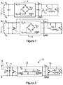
- FIG. 1 two forms of implementations of shunt regulator for LF and HF applications can be distinguished in the prior art, as shown in simplified form in figure 1 , denoted by A and B.
- a and B In both circuits there is a coil 3, connected to an AC side of a rectifier 2.
- a load resistor R L represents the circuit supplied by the DC side of the rectifier 2.
- an active load transistor 1 is used in a control loop to directly regulate a DC output of the rectifier 2.
- the active load device in CMOS implementations is typically an N-type transistor 1 (NMOST).
- NMOST N-type transistor 1
- a differential amplifier 4 provides a positive bias signal to the NMOST 1 when the DC output voltage V DD from the rectifier 2 exceeds a reference voltage V ref .
- the rectifier structure found in most implementations may be a hybrid type using a cross-coupled pair of transistors as pass devices with regard to chip ground.
- the negative swing relative to ground may be small in relation to the overall input amplitude.
- the pass devices of the rectifier 2 with respect to the positive supply V DD could be ordinary PN diodes or Schottky diodes, but in most cases are MOS transistors in diode configuration, hence with shorted gate-drain nodes.
- circuit A in figure 1 it can be seen that the complete excess current is passed though the rectifier 2.
- relatively high RMS currents may occur at maximum field strength (for instance 40 mA at a field strength of 7.5 A/m)
- the difference between regulated DC voltage level and AC amplitude at the coil caused by the voltage drop at the rectifying devices does usually not exceed 1 V due to the non-linear characteristic of the pass devices of the rectifier 2.
- circuit version B the voltage drop is even smaller, as the excess current is shunted directly at the coil terminal (before it reaches the rectifier 2).
- a low quality (Q) factor at minimum DC load is desirable to allow a broadband impedance matching of antenna and IC.
- Q factor in the range of 15 may be appropriate, corresponding to a bandwidth of larger than 150 MHz at UHF frequencies.
- the associated minimum input RF amplitude at the frontend to achieve this Q factor may typically be below 300 mV.
- Differential frontends typically may use Dickson like circuits, or may use cross-coupled bridge type charge-pumps.
- the ESD structures 11 and modulating transistor 14 as depicted in figure 2 are typically connected in a differential implementation in mirrored form with respect to the chip ground.
- the pass devices of the charge-pumps in UHF transponders are not directly connected to the input RF node, but instead need to be coupled capacitively (i.e. via a capacitor) thereto.
- DC side voltage regulators are predominantly employed, and the shunted excess current is limited in consequence by the size of the coupling capacitors for a given input power. The input voltage amplitude therefore rises significantly with increasing input power.
- ground connected transistors may be associated with the modulator circuitry 14, and may also be present in the ESD protection circuit. In CMOS implementations, such transistors are typically NMOS transistors. Despite the strong non-linear characteristic of these devices, the voltage amplitude observed at a maximum operating input power of 20 dBm may still reach 1 V.
- UHF RFID ICs are based on CMOS technologies featuring minimum channel lengths of around 140 nm. Typical maximum operating voltages of such MOS devices lie in the range of 1.8 V. With progressing technology and decreasing minimum feature size, maximum voltage ratings decrease. For example, for 90 nm and 40 nm technologies operating voltage limits of around 1.3 V and 1.2 V have to be considered. In single-ended frontends, although such reduced limits may still lie above the estimated clamping voltage of 1 V provided by anti-parallel ESD diodes, the margin is substantially decreased. For differential frontends, due to the series connection of two diodes between the symmetrical RF nodes, the clamping voltage is approximately doubled and the voltage limits might be exceeded. In order to maintain the desired specifications on maximum operating power the voltage-limiting structures associated with differential PCUs have to be changed when moving to advanced technologies.
- a known solution to enhance the voltage limiting arrangement of figure 2 is to use a NMOS active load connected directly at the RF terminal with a positive control voltage, as already described in conjunction with HF frontends.
- FIG. 3 shows a UHF transponder frontend 20, comprising a UHF antenna 21.
- one terminal 21 b of the antenna 21 is grounded.
- the signal from the non-grounded antenna terminal 21 a provides the RF input RF A to an RF input rail 27 of the frontend 20.
- An ESD protection circuit 22 is included, comprising a pair of anti-parallel ESD protection diodes 11 connected between a ground rail 28 and the RF input rail 27.
- a modulating transistor 14 is connected between the RF input rail 27 and ground 28. The gate of the modulating transistor 14 is connected to a data input terminal 23, so that the characteristics of the antenna 21 are modulated in accordance with the data signal 23.
- a voltage limiter 24 comprising an NMOS limiting transistor 1 is connected between the RF rail 27 and the ground rail 28.
- a positive bias voltage V bN is provided for the NMOS limiting transistor 1.
- the positive bias voltage V bN controls the source-drain current through the limiting transistor 1.
- the active-load device might be incorporated in the ESD circuit 22.
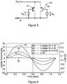
- FIG. 4 shows a plot of the RF input voltage 41 with respect to time compared to the source drain current through the limiting transistor 1.
- Source drain currents for bias voltages of 0 V, 0.6 V and 1 V are shown in curves 42, 43 and 44 respectively.
- the potential between gate and ground node of the limiting transistor 1 corresponds to the gate source voltage of the limiting transistor 1.
- This voltage can be assumed to be fixed during one period. In consequence the limiting transistor 1 is either non-conductive at all or is driven increasingly towards a saturation region of operation with rising amplitude.
- the potential difference between the RF node and the gate determines the effective gate source voltage.
- the limiting transistor 1 gets progressively more conductive causing the strongly asymmetrical current waveforms 44, 43 and 42 shown in figure 3 . It is notable that this behaviour may also be observed if no limiting transistor is present.
- any virtually ground-connected NMOS devices present in the modulator 14 provide the primary shunt path.
- the NMOS dominated structure does not behave symmetrically. This imbalance has the inevitable effect that at higher voltage amplitudes the DC potential at the RF input node rises with respect to chip ground.
- the ground connected NMOS structures behave as a parasitic charge-pump.
- Figure 4 simplifies the RF voltage waveform 41 as an ideal sine wave, which does not realistically reflect the behaviour at an UHF frontend since the antenna impedance is neglected. Nevertheless, the observed asymmetrical current flow characteristic through the NMOS limiting transistor is a real effect that occurs in operation. Voltage and current transients at the RF port are directly related to back-scattered signals from the antenna, so the asymmetrical behaviour as indicated by figure 4 may cause significant harmonic radiation from the antenna 15 at higher input power levels. It also should be noted that UHF RFID transponders are subject to frequency regulation like standard RF devices, and such radiated harmonics may be particularly undesirable in this respect.
- a voltage converter comprising:
- the voltage limiting circuit may further comprise a biasing means operable to generate a positive and negative bias voltage for controlling the operation of the NMOS and PMOS limiting transistors respectively.
- the biasing means may be configured to provide symmetric bias potentials to the NMOS and PMOS limiting transistors.
- the biasing means may comprise a charge pump.
- the charge pump may be arranged to generate a bias potential for a limiting transistor.
- a charge pump may be arranged to generate a negative bias potential from the RF signal.
- the charge pump may provide the negative bias potential to the PMOS limiting transistor.
- the biasing means may comprise a first charge pump and a second charge pump, wherein the first charge pump is arranged to generate a negative bias signal from the RF signal, and the second charge pump is arranged to generate a positive bias signal from the RF signal.
- At least one charge pump of the biasing means may be configured with a minimum input voltage amplitude below which the charge pump is inoperable.
- the minimum input voltage amplitude for operating the charge pump may be greater than 0.3 V.
- the minimum input voltage amplitude for operating the charge pump may be greater than 0.1 V, 0.2 V, or 0.4V.
- the biasing means may comprise a resistive load connected to a gate of each limiting transistor.
- the biasing means may comprise a transistor connected to the gate of each limiting transistor.
- the voltage limiting circuit may be connected between the RF input terminal and ground.
- the AC-DC converter may be configured for connection to a differential RF input comprising a first and second RF input terminal, such that the voltage limiting circuit is arranged between the first and second RF terminals.
- the voltage limiting circuit may have a substantially symmetric response to positive and negative over voltage of the RF signal.
- the circuit may be for a UHF transponder.
- a radio frequency transponder comprising: an antenna, the voltage converter of the first aspect of the invention, a demodulator for receiving data from the antenna and a modulator for transmitting data via the antenna, wherein the voltage limiting circuit is arranged to regulate the amplitude of an RF signal from the antenna.
- a voltage limiting circuit 50 comprising an NMOS limiting transistor 52 and a PMOS limiting transistor 51.
- the NMOS and PMOS limiting transistors 52, 51 are connected in parallel between the RF signal V RF and ground GND, so that they can shunt excess RF signal voltage to ground.
- a negative bias voltage source V bP is connected to the gate of the PMOS limiting transistor 51, and a positive bias voltage source V bN is connected to the gate of the NMOS limiting transistor 52.
- the bias voltage sources that generate V bN and V bP may be configured to provide symmetric bias potentials to the limiting transistors 51, 52, so that the transient voltage-current characteristic of the voltage limiting circuit 50 is symmetric for positive and negative voltage swings.
- Figure 6 shows the symmetric voltage-current characteristic of the voltage limiting circuit 50 of figure 5 .
- a plot of the RF input voltage 41 with respect to time is shown compared to the current through the voltage limiting circuit 50.
- Currents for bias voltages V bN and V bP having a magnitude of 0 V, 0.6 V and 1 V are shown in waveforms 42, 43 and 44 respectively.
- the waveforms 42, 43 and 44 are balanced, with the current during the negative part of the cycle balancing the current during the positive part of the cycle.
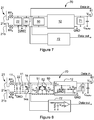
- FIG 7 is a block diagram of a voltage converter 70 according to an embodiment connected to a UHF antenna 21. A more specific embodiment is shown in figure 8 , in which example circuit elements are shown.
- the UHF antenna 21 comprises a first terminal 21 a and a second terminal 21 b.
- the embodiments of figures 7 and 8 comprise single ended front ends, in which the second terminal 21 b is grounded, so that the first terminal 21a provides the RF input signal RF A .
- the voltage converter 70 comprises: ESD protection circuit 22, modulator 14, demodulator 72, RF limiting circuit 50, charge pump 12 and DC limiting circuit 71.
- a DC output signal VDD is provided at a DC output terminal 81.
- the ESD protection circuit 22 is for protecting the voltage converter 70 from high input voltages, and may comprise anti-parallel diodes (as shown in figure 8 ).
- the modulator 14 is for transmitting data via the antenna 21, and may comprise a variable load for modulating the characteristics of the antenna 21.
- the modulator comprises a modulating transistor 14a.
- the demodulator 72 receives the RF input signal from the antenna 21 and demodulates it to receive data from the antenna 21.
- the demodulator 72 may comprise an AM diode detector demodulator with an associated comparator (as shown in figure 8 ).
- the charge pump 12 converts the RF input signal RF A to a DC output voltage V DD which may be used to provide power to at least some of the voltage converter 70, or to other components.
- the charge pump 12 may comprise a Dickson charge pump (as shown in figure 8 ), and may be a different type of charge pump.
- the DC limiting circuit 71 regulates the DC output voltage from the charge pump 12.
- the DC limiting circuit 71 may comprise a Zener diode (as shown in figure 8 ), or another arrangement, which may comprise active elements, that approximates a Zener diode.
- the RF limiting circuit 50 comprises a parallel complimentary PMOS and NMOS transistor 51, 52 and associated negative and positive bias means V bP , V bN (as shown in figure 8 ).
- the RF limiting circuit provides a balanced transient voltage-current characteristic, which will suppress the generation of even order harmonic components in the frequency domain. This prevents related harmonic components in the backscattered signal of the antenna 21.
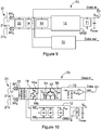
- Figures 9 and 10 show alternative differential embodiments, in which first and second antenna terminals 21a 21b provide differential RF signals RF A and RF B .
- the same basic circuit blocks are present, but may be slightly modified to reflect the differential arrangement.
- the ESD protection circuit 22 may comprise a pair of anti-parallel diodes for each antenna terminal 21 a, 21 b, arranged to shunt excess voltage from each RF signal directly to ground.
- the modulator 14 may comprise NMOS load transistors 14a, 14b for each antenna terminal 21 a, 21 b symmetrically connected to ground.
- the RF limiting circuit 50 may be connected between the differential RF signal lines carrying RF A and RF B , so that when the differential RF voltage is too high, current is shunted between the differential RF signal lines.
- the RF limiting circuit 50 may be arranged to shunt current from each of the differential signal lines to ground. Connecting the RF limiting circuit 50 between the RF nodes allows the dimensions of the device to be minimised while achieving a certain impedance limit required at higher input voltages. Connecting the RF limiting circuit 50 between the RF nodes corresponding with RF A , RF B is synergistic with the symmetric voltage current characteristics of the RF limiting circuit 50.
- the voltage limiting circuit 50 and the modulator 14 were NMOS dominated (as in prior art arrangements), at higher RF voltage amplitudes the common mode potential at the input would rise with respect to chip ground, because the ground connected NMOS structures would act as a charge pump, compromising the shunting efficiency of the voltage limiting circuit 50.
- FIG 11 shows an example of an RF limiting circuit 50 in more detail.
- the RF limiting circuit 50 comprises a PMOS limiting transistor 51 and an NMOS limiting transistor 52 which are arranged to shunt excess RF input voltage V RF to ground GND.
- a negative bias generator circuit 53 is provided for generating the bias voltage V bP at the gate of the PMOS limiting transistor 51
- a positive bias generator circuit 54 is provided for generating the bias voltage V bN at the gate of the NMOS limiting transistor 52.
- Both the positive and negative bias generator circuits 53, 54 employ Dickson charge pumps to produce the bias potentials V bP , V bN from the RF input signal V RF by driving current through a resistive load 56 connected to the limiting transistor gate.
- the Dickson charge pumps comprise transistors 55 wired as diodes, coupled to the RF signal and ground via capacitors. Such MOS diodes do not allow significant charge transfer until the input voltage amplitude exceeds the threshold voltage of the transistor. Subsequent to this, the DC output rises linearly with increasing input amplitude.
- separate stages of the main charge pump 12 conventionally include additional circuitry to compensate for this dead-zone effect by pre-biasing the gates of the MOS transistors of the charge pump, so as to enable minimum operating thresholds of below 300mV. In most cases the threshold at which the charge pump is operable is significantly below the threshold voltage of the transistors thereof.
- the MOS transistors of the charge pump may have threshold values in the range of 300mV to 500 mV. Specifically designed MOS transistors with raised threshold voltage may be used in the RF limiting circuit to tailor the response of the circuit.
- the RF limiting circuit 50 is not operable. As a certain level of input power and therewith voltage amplitude is exceeded the bias potentials V bP and V bN rise in magnitude and therefore progressively reduce the equivalent parallel input impedance of the RF limiting circuit 50 circuit with respect to the RF node RF A .
- the RF limiting circuit 50 may be operated in concert with a voltage limiter 71 on the DC bus, which may accurately regulate the internal DC voltage supply. Therefore only a rough control mechanism may be necessary for the RF voltage limiter 50. A specific value of load impedance at the output of the auxiliary charge-pumps might suffice.
- the charge-pumps 53, 54 are inactive and the bias potentials V bP , V bN are essentially zero.
- the gate-source voltage swing observed at the limiting transistors 51, 52 remains below their threshold and the RF limiting circuit 50 shows high impedance therefore allowing maximum power conversion efficiency of the overall PCU.
- the charge-pumps 53, 54 become active and the bias potentials V bP , V bN rise in magnitude. Effectively the gate-source voltages of the limiting transistors 51, 52 rise in response to the increasing voltage swing and the additionally provided bias.
- the input impedance of the RF limiter 50 may drop by several decades in absolute value keeping the input amplitude below the operating voltage limits of involved transistors at maximum input power.
- Some design parameters of the RF limiting circuit which may be varied include the dimensions of the limiting transistors 51, 52; the number of stages in each of the charge-pumps 53, 54, and the value of load impedance 56. These parameters mainly determine the sensitivity of the biasing of the limiting transistors 51, 52 with respect to the RF input amplitude. The transient behaviour depends on the RC constant found at the gates of the limiting transistors 51, 52.
- FIG 12 shows an alternative embodiment in which a non-linear load impedance is employed, which may achieve an enhancement of the impedance characteristic over input amplitude.
- the load resistors 56 are replaced with transistors 57.
- the additional transistors 57 resemble, in principle, current sources.
- the load transistors 57 show low impedance with respect to ground.
- the load transistors 57 would have to be provided with a positive bias potential V bPS and negative bias potential V bNS respectively. Providing the negative bias potential V bPS in particular may require additional effort.
- the limiting transistors 51, 52 can be placed directly between the two RF nodes RF A , RF B or symmetrically between each RF node and ground. This is true not only for the RF limiting transistors 51, 52, but also for the transistors of the modulator 14, utilized for backscatter communication.
- Inserting limiting transistors 51, 52 serially between the RF nodes and centred towards chip ground might be preferred in some embodiments in order to allow integration of the structures into the overall ESD concept.
- N-type devices are used. Considering only the individual RF nodes with reference to ground, such an NMOS dominated structure does not behave symmetrically. This imbalance has the inevitable effect that at higher voltage amplitudes the common mode potential at the input rises with respect to chip ground.
- the ground connected NMOS structures behave as a parasitic charge-pump.
- the embodiment of figure 13 comprises a differential charge-pump 53 for generating the negative bias voltage V bP and a differential charge-pump 54 for generating the positive bias voltage V bN .
- a single stage charge-pump 53 is shown, comprising an NMOS and PMOS transistor.
- the central node of one branch of the charge pump stage is coupled to the first RF signal V RFA via a coupling capacitor, and the central node of the other branch of the charge pump is connected to V RFB via a further coupling capacitor.
- both branches of the charge pump stage are connected together and are connected to ground via a coupling capacitor.
- the gates of the transistors of each branch of each stage are connected to the central node of the other branch in a crossover arrangement.
- a resistive load 56 is provided connected to the gate of each of the limiting transistors 51, 52.
- the complementary active-load structure at the PMOS limiting transistor 51 comprises a pair of PMOS transistors 57a, 57b.
- a first PMOS transistor 57a has a source connected to the first RF signal V RFA , a gate connected to the gate of the PMOS limiting transistor 51, and a drain connected to ground.
- a second PMOS transistor 57b has a drain connected to the first PMOS transistor drain, a gate connected to the first PMOS transistor gate and a source connected to the second RF signal V RFB .
- the complementary load active-load structure at the NMOS limiting transistor 52 comprises a corresponding arrangement of NMOS transistors.
Landscapes
- Engineering & Computer Science (AREA)
- Computer Hardware Design (AREA)
- Microelectronics & Electronic Packaging (AREA)
- Power Engineering (AREA)
- Physics & Mathematics (AREA)
- General Physics & Mathematics (AREA)
- Theoretical Computer Science (AREA)
- Computer Networks & Wireless Communication (AREA)
- Signal Processing (AREA)
- Dc-Dc Converters (AREA)
- Semiconductor Integrated Circuits (AREA)
- Near-Field Transmission Systems (AREA)
Claims (15)
- Ein Spannungskonverter (70) aufweisend:einen AC-DC Konverter, welcher mit einem RF Eingangsanschluss (21a, 21b) und einem DC Ausgangsanschluss (81) verbunden ist und welcher funktionsfähig ist zum Konvertieren eines RF Signals an dem RF Eingangsanschluss (21a, 21b) zu einem DC Ausgangssignal an dem DC Ausgangsanschluss (81); undeinen Spannungsbegrenzungsschaltkreis (50), welcher mit dem RF Eingangsanschluss (21a, 21b) verbunden ist und welcher funktionsfähig ist zum Begrenzen der Amplitude des RF Signals;dadurch gekennzeichnet, dass
der Spannungsbegrenzungsschaltkreis einen NMOS begrenzenden Transistor (52) aufweist, welcher parallel zu einem komplementären PMOS begrenzenden Transistor (51) geschaltet ist. - Der Spannungskonverter gemäß Anspruch 1, wobei der Spannungsbegrenzungsschaltkreis ferner ein Vorspannmittel aufweist, welches funktionsfähig ist zum Erzeugen einer positiven und negativen Vorspannung zum jeweiligen Steuern des Betriebs des NMOS und PMOS begrenzenden Transistors.
- Der Spannungskonverter gemäß Anspruch 2, wobei das Vorspannmittel konfiguriert ist zum Bereitstellen von symmetrischen Vorspannungspotenzialen an dem NMOS und dem PMOS begrenzenden Transistor.
- Der Spannungskonverter gemäß Anspruch 3, wobei das Vorspannmittel eine Ladungspumpe aufweist.
- Der Spannungskonverter gemäß Anspruch 4, wobei das Vorspannmittel eine Ladungspumpe aufweist, welche eingerichtet ist zum Erzeugen eines negativen Vorspannungspotenzials aus dem RF Signal.
- Der Spannungskonverter gemäß Anspruch 5, wobei das Vorspannmittel eine erste Ladungspumpe und eine zweite Ladungspumpe aufweist, wobei die erste Ladungspumpe eingerichtet ist zum Erzeugen eines negativen Vorspannungssignals aus dem RF Signal und die zweite Ladungspumpe eingerichtet ist zum Erzeugen eines positiven Vorspannungssignals aus dem RF Signal.
- Der Spannungskonverter gemäß irgendeinem der Ansprüche 4 bis 6, wobei zumindest eine Ladungspumpe des Vorspannmittels mit einer minimalen Eingangsspannungsamplitude konfiguriert ist, unter welcher die Ladungspumpe nicht funktionsfähig ist.
- Der Spannungskonverter gemäß Anspruch 7, wobei die minimale Eingangsspannungsamplitude größer als 0,3 V ist.
- Der Spannungskonverter gemäß irgendeinem der Ansprüche 2 bis 8, wobei das Vorspannmittel eine ohmsche Last aufweist, welche mit einem Gate von jedem begrenzenden Transistor verbunden ist.
- Der Spannungskonverter gemäß irgendeinem der Ansprüche 2 bis 8, wobei das Vorspannmittel einen Transistor aufweist, welcher mit dem Gate von jedem begrenzenden Transistor verbunden ist.
- Der Spannungskonverter gemäß irgendeinem vorangehenden Anspruch, wobei der Spannungsbegrenzungsschaltkreis zwischen den RF Eingangsanschluss und Masse geschaltet ist.
- Der Spannungskonverter gemäß irgendeinem vorangehenden Anspruch, wobei der AC-DC Konverter konfiguriert ist für eine Verbindung zu einem differentiellen RF Eingang, welcher einen ersten und einen zweiten RF Eingangsanschluss aufweist, so dass der Spannungsbegrenzungsschaltkreis zwischen dem ersten und dem zweiten RF Anschluss angeordnet ist.
- Der Spannungskonverter gemäß irgendeinem vorangehenden Anspruch, wobei der Spannungsbegrenzungsschaltkreis eine im Wesentlichen symmetrische Reaktion auf eine positive und eine negative Überspannung des RF Signals hat.
- Der Spannungskonverter gemäß irgendeinem vorangehenden Anspruch, wobei der Spannungskonverter zum Bereitstellen einer DC Spannung zu einem UHF Transponder ist.
- Ein Radiofrequenz Transponder aufweisend:eine Antenne,den Spannungskonverter gemäß irgendeinem vorangehenden Anspruch,einen Demodulator zum Empfangen von Daten von der Antenne, undeinen Modulator zum Übertragen von Daten via die Antenne, wobei der Spannungsbegrenzungsschaltkreis eingerichtet ist zum Regeln der Amplitude eines RF Signals von der Antenne.
Priority Applications (3)
| Application Number | Priority Date | Filing Date | Title |
|---|---|---|---|
| EP14175820.1A EP2963587B1 (de) | 2014-07-04 | 2014-07-04 | Spannungswandler |
| US14/791,230 US9716443B2 (en) | 2014-07-04 | 2015-07-02 | Voltage converter |
| CN201510387818.8A CN105322813B (zh) | 2014-07-04 | 2015-07-03 | 电压转换器 |
Applications Claiming Priority (1)
| Application Number | Priority Date | Filing Date | Title |
|---|---|---|---|
| EP14175820.1A EP2963587B1 (de) | 2014-07-04 | 2014-07-04 | Spannungswandler |
Publications (2)
| Publication Number | Publication Date |
|---|---|
| EP2963587A1 EP2963587A1 (de) | 2016-01-06 |
| EP2963587B1 true EP2963587B1 (de) | 2017-03-15 |
Family
ID=51162512
Family Applications (1)
| Application Number | Title | Priority Date | Filing Date |
|---|---|---|---|
| EP14175820.1A Active EP2963587B1 (de) | 2014-07-04 | 2014-07-04 | Spannungswandler |
Country Status (3)
| Country | Link |
|---|---|
| US (1) | US9716443B2 (de) |
| EP (1) | EP2963587B1 (de) |
| CN (1) | CN105322813B (de) |
Cited By (1)
| Publication number | Priority date | Publication date | Assignee | Title |
|---|---|---|---|---|
| US12380309B2 (en) | 2023-11-17 | 2025-08-05 | Nxp B.V. | Radio frequency voltage limiter for an RFID transponder |
Families Citing this family (14)
| Publication number | Priority date | Publication date | Assignee | Title |
|---|---|---|---|---|
| US8749319B2 (en) * | 2006-11-18 | 2014-06-10 | Rfmicron, Inc. | Method and apparatus for detecting RF field strength |
| EP2830229B1 (de) * | 2013-07-25 | 2017-04-19 | Nxp B.V. | Mehrkanaliger Transponder und Verfahren zur Bestimmung eines am stärksten gekoppelten Kanals oder noch stärker gekoppelter Kanäle |
| EP2963587B1 (de) * | 2014-07-04 | 2017-03-15 | Nxp B.V. | Spannungswandler |
| ES2748649T3 (es) * | 2016-04-22 | 2020-03-17 | Farsens S L | Etiqueta de identificación por radiofrecuencia (RFID) y método para limitar la tensión de suministro de una etiqueta de RFID |
| FR3054948A1 (fr) * | 2016-08-04 | 2018-02-09 | Stmicroelectronics (Rousset) Sas | Circuit et procede de protection de moyens de regulation de tension contre les decharges electrostatiques |
| EP3614545B1 (de) * | 2017-04-28 | 2022-02-23 | Panasonic Intellectual Property Management Co., Ltd. | Stromversorgungsschaltung |
| JP6844478B2 (ja) * | 2017-09-14 | 2021-03-17 | オムロン株式会社 | Rfタグ |
| JP6855989B2 (ja) * | 2017-09-14 | 2021-04-07 | オムロン株式会社 | Rfタグ回路 |
| JP7028653B2 (ja) | 2018-01-17 | 2022-03-02 | ローム株式会社 | 絶縁同期整流型dc/dcコンバータ |
| CN110110563B (zh) * | 2019-03-14 | 2022-06-07 | 上海诺潇智能科技有限公司 | 一种rfid基带信号调制深度的实现方法 |
| EP3726715B1 (de) * | 2019-04-15 | 2021-09-15 | Nxp B.V. | Fehlererkennung in hybriden gleichstromwandlern |
| US11764204B2 (en) * | 2020-06-18 | 2023-09-19 | Analog Devices, Inc. | Electrostatic discharge and overdrive protection circuitry |
| US11664681B2 (en) * | 2021-06-30 | 2023-05-30 | Arm Limited | Device and/or method for wireless signal detection |
| EP4567662A1 (de) * | 2023-12-08 | 2025-06-11 | Nxp B.V. | Frontendschaltung für einen rfid-transponder |
Family Cites Families (30)
| Publication number | Priority date | Publication date | Assignee | Title |
|---|---|---|---|---|
| US613413A (en) | 1898-11-01 | Atomizer | ||
| US5045770A (en) | 1988-02-04 | 1991-09-03 | Magellan Corporation (Aust.) Pty. Ltd. | Shunt regulator for use with resonant input source |
| US5252911A (en) * | 1989-08-03 | 1993-10-12 | Banura George A | AC to DC power converter with regulated bi-polar outputs |
| JP3201910B2 (ja) * | 1994-07-06 | 2001-08-27 | シャープ株式会社 | バッファ回路及び画像表示装置 |
| JPH08274184A (ja) * | 1995-03-31 | 1996-10-18 | Toshiba Microelectron Corp | 半導体集積回路の保護回路装置 |
| ATA91895A (de) | 1995-05-31 | 1997-11-15 | Mikron Ges Fuer Integrierte Mi | Versorgungsspannungsaufbereitungsschaltung sowie datenträger mit einer versorgungsspannungsaufbereitungsschaltung |
| US5815355A (en) * | 1997-10-06 | 1998-09-29 | Atmel Corporation | Modulation compensated clamp circuit |
| US6134130A (en) | 1999-07-19 | 2000-10-17 | Motorola, Inc. | Power reception circuits for a device receiving an AC power signal |
| DE10109768A1 (de) * | 2001-03-01 | 2002-09-05 | Power One Ag Uster | Spannungskonverter |
| DE102004013177B4 (de) | 2004-03-17 | 2006-05-18 | Infineon Technologies Ag | Datenübertragungseinheit mit einer Datenübertragungsschnittstelle und ein Verfahren zum Betreiben der Datenübertragungseinheit |
| US7236763B2 (en) * | 2004-06-04 | 2007-06-26 | Motorola, Inc. | Method and apparatus providing improved mixer performance for radio receivers |
| US8045947B2 (en) * | 2004-09-17 | 2011-10-25 | Massachusetts Institute Of Technology | RF power extracting circuit and related techniques |
| KR100682059B1 (ko) * | 2005-02-24 | 2007-02-15 | 삼성전자주식회사 | 초 저전력 과전압 보호회로 |
| US7890891B2 (en) * | 2005-07-11 | 2011-02-15 | Peregrine Semiconductor Corporation | Method and apparatus improving gate oxide reliability by controlling accumulated charge |
| US8292185B2 (en) * | 2005-09-30 | 2012-10-23 | Stmicroelectronics Asia Pacific Pte., Ltd. | Circuits for preventing overvoltage conditions on antenna terminals and method |
| ATE534971T1 (de) * | 2005-12-15 | 2011-12-15 | Nxp Bv | Hochfrequenz-schnittstellenschaltung für ein hochfrequenz-indentifikationsetikett |
| DE502007006276D1 (de) * | 2006-02-15 | 2011-02-24 | Atmel Automotive Gmbh | Verfahren zur Spannungsbegrenzung bei einem Transponder |
| US7990249B1 (en) | 2006-08-03 | 2011-08-02 | Impinj, Inc. | RFID tag circuits tags and methods for backscattering with controllable admittance |
| DE102007004843A1 (de) | 2007-01-31 | 2008-08-07 | Infineon Technologies Ag | Konzept zum Bereitstellen einer Versorgungsspannung und einer Lastmodulation in einem Transponder |
| US8314685B2 (en) | 2007-08-27 | 2012-11-20 | Texas Instruments Incorporated | Data detector for UHF RFID tags |
| US7786720B2 (en) * | 2008-06-26 | 2010-08-31 | Telefonaktiebolaget Lm Ericsson (Publ) | Passive mixer power detector method and apparatus |
| US8280259B2 (en) * | 2009-11-13 | 2012-10-02 | Corning Cable Systems Llc | Radio-over-fiber (RoF) system for protocol-independent wired and/or wireless communication |
| US8624675B2 (en) * | 2010-03-25 | 2014-01-07 | Lloyd Lautzenhiser | Method and system for providing automatic gate bias and bias sequencing for field effect transistors |
| US8963643B2 (en) * | 2010-03-25 | 2015-02-24 | Emhiser Research Limited | Method and system for providing automatic gate bias and bias sequencing for field effect transistors |
| US20130043735A1 (en) * | 2011-08-16 | 2013-02-21 | Qualcomm Incorporated | Systems, methods, and devices for multi-level signaling via a wireless power transfer field |
| US9252846B2 (en) * | 2011-09-09 | 2016-02-02 | Qualcomm Incorporated | Systems and methods for detecting and identifying a wireless power device |
| TW201328153A (zh) * | 2011-12-16 | 2013-07-01 | Ind Tech Res Inst | 微功率整流器及其方法 |
| US9001529B2 (en) * | 2012-01-17 | 2015-04-07 | Texas Instruments Incorporated | System and method for power transfer control based on available input power |
| CN103647539B (zh) * | 2013-11-08 | 2017-01-11 | 上海华力微电子有限公司 | 开关装置及具有该开关装置的多通道耦合选择器 |
| EP2963587B1 (de) * | 2014-07-04 | 2017-03-15 | Nxp B.V. | Spannungswandler |
-
2014
- 2014-07-04 EP EP14175820.1A patent/EP2963587B1/de active Active
-
2015
- 2015-07-02 US US14/791,230 patent/US9716443B2/en active Active
- 2015-07-03 CN CN201510387818.8A patent/CN105322813B/zh active Active
Non-Patent Citations (1)
| Title |
|---|
| None * |
Cited By (1)
| Publication number | Priority date | Publication date | Assignee | Title |
|---|---|---|---|---|
| US12380309B2 (en) | 2023-11-17 | 2025-08-05 | Nxp B.V. | Radio frequency voltage limiter for an RFID transponder |
Also Published As
| Publication number | Publication date |
|---|---|
| US9716443B2 (en) | 2017-07-25 |
| US20160006369A1 (en) | 2016-01-07 |
| CN105322813B (zh) | 2018-04-24 |
| CN105322813A (zh) | 2016-02-10 |
| EP2963587A1 (de) | 2016-01-06 |
Similar Documents
| Publication | Publication Date | Title |
|---|---|---|
| EP2963587B1 (de) | Spannungswandler | |
| US6134130A (en) | Power reception circuits for a device receiving an AC power signal | |
| US7703677B2 (en) | Rectifier circuit | |
| US20120049937A1 (en) | High efficiency charge pump | |
| TWI708187B (zh) | 用於射頻(rf)標籤的接收器單元 | |
| KR101843433B1 (ko) | 전압 조정 회로, 이를 포함하는 비접촉식 카드, 및 비접촉식 카드 시스템 | |
| US7738272B2 (en) | Circuit and method for rectifying and regulating voltages | |
| KR100700849B1 (ko) | 반도체 집적회로, 반도체 집적회로를 구비하는 무접촉정보매체, 및 반도체 집적회로를 구동하는 방법 | |
| US7732945B2 (en) | Rectifier circuit | |
| KR20070098939A (ko) | 션트 레귤레이터 및 전자 기기 | |
| US10056787B2 (en) | Rectifier circuit, and contactless power supply device | |
| CN107251353B (zh) | 近场通讯nfc设备 | |
| WO2018000703A1 (zh) | 一种整流电路和具有该整流电路的特高频标签 | |
| EP4560527A1 (de) | Radiofrequenz-spannungsbegrenzer für einen rfid-transponder | |
| US8328105B2 (en) | Semiconductor device | |
| Zoscher et al. | RF voltage limiters for passive differential UHF RFID front-ends in a 40 nm CMOS technology | |
| KR101822491B1 (ko) | 전압 조정 회로 및 이의 동작 방법 | |
| CN103270521A (zh) | 具有可调衰减器元件的用于接收低频电磁波的电子电路装置 | |
| US9906064B2 (en) | Receiver circuit | |
| JP2006238693A (ja) | 過電圧保護回路 | |
| US20160072402A1 (en) | Rectifying circuit and contactless ic card | |
| Liu et al. | A low input power charge pump for passive UHF RFID applications | |
| San Martin et al. | RFID front-end in 0.5 μm standard CMOS process: Experimental results | |
| HK1230320B (zh) | 用於射频标签的接收器单元 | |
| HK1230320A1 (en) | Receiver unit for an rf tag |
Legal Events
| Date | Code | Title | Description |
|---|---|---|---|
| PUAI | Public reference made under article 153(3) epc to a published international application that has entered the european phase |
Free format text: ORIGINAL CODE: 0009012 |
|
| AK | Designated contracting states |
Kind code of ref document: A1 Designated state(s): AL AT BE BG CH CY CZ DE DK EE ES FI FR GB GR HR HU IE IS IT LI LT LU LV MC MK MT NL NO PL PT RO RS SE SI SK SM TR |
|
| AX | Request for extension of the european patent |
Extension state: BA ME |
|
| 17P | Request for examination filed |
Effective date: 20160706 |
|
| RBV | Designated contracting states (corrected) |
Designated state(s): AL AT BE BG CH CY CZ DE DK EE ES FI FR GB GR HR HU IE IS IT LI LT LU LV MC MK MT NL NO PL PT RO RS SE SI SK SM TR |
|
| GRAP | Despatch of communication of intention to grant a patent |
Free format text: ORIGINAL CODE: EPIDOSNIGR1 |
|
| STAA | Information on the status of an ep patent application or granted ep patent |
Free format text: STATUS: GRANT OF PATENT IS INTENDED |
|
| RIC1 | Information provided on ipc code assigned before grant |
Ipc: H02M 7/217 20060101ALI20161116BHEP Ipc: H04B 1/40 20060101ALI20161116BHEP Ipc: G06K 19/07 20060101AFI20161116BHEP |
|
| INTG | Intention to grant announced |
Effective date: 20161130 |
|
| GRAS | Grant fee paid |
Free format text: ORIGINAL CODE: EPIDOSNIGR3 |
|
| GRAA | (expected) grant |
Free format text: ORIGINAL CODE: 0009210 |
|
| STAA | Information on the status of an ep patent application or granted ep patent |
Free format text: STATUS: THE PATENT HAS BEEN GRANTED |
|
| AK | Designated contracting states |
Kind code of ref document: B1 Designated state(s): AL AT BE BG CH CY CZ DE DK EE ES FI FR GB GR HR HU IE IS IT LI LT LU LV MC MK MT NL NO PL PT RO RS SE SI SK SM TR |
|
| REG | Reference to a national code |
Ref country code: CH Ref legal event code: EP Ref country code: GB Ref legal event code: FG4D |
|
| REG | Reference to a national code |
Ref country code: IE Ref legal event code: FG4D |
|
| REG | Reference to a national code |
Ref country code: AT Ref legal event code: REF Ref document number: 876261 Country of ref document: AT Kind code of ref document: T Effective date: 20170415 |
|
| REG | Reference to a national code |
Ref country code: DE Ref legal event code: R096 Ref document number: 602014007522 Country of ref document: DE |
|
| REG | Reference to a national code |
Ref country code: FR Ref legal event code: PLFP Year of fee payment: 4 |
|
| REG | Reference to a national code |
Ref country code: NL Ref legal event code: MP Effective date: 20170315 |
|
| REG | Reference to a national code |
Ref country code: LT Ref legal event code: MG4D |
|
| PG25 | Lapsed in a contracting state [announced via postgrant information from national office to epo] |
Ref country code: LT Free format text: LAPSE BECAUSE OF FAILURE TO SUBMIT A TRANSLATION OF THE DESCRIPTION OR TO PAY THE FEE WITHIN THE PRESCRIBED TIME-LIMIT Effective date: 20170315 Ref country code: NO Free format text: LAPSE BECAUSE OF FAILURE TO SUBMIT A TRANSLATION OF THE DESCRIPTION OR TO PAY THE FEE WITHIN THE PRESCRIBED TIME-LIMIT Effective date: 20170615 Ref country code: HR Free format text: LAPSE BECAUSE OF FAILURE TO SUBMIT A TRANSLATION OF THE DESCRIPTION OR TO PAY THE FEE WITHIN THE PRESCRIBED TIME-LIMIT Effective date: 20170315 Ref country code: FI Free format text: LAPSE BECAUSE OF FAILURE TO SUBMIT A TRANSLATION OF THE DESCRIPTION OR TO PAY THE FEE WITHIN THE PRESCRIBED TIME-LIMIT Effective date: 20170315 Ref country code: GR Free format text: LAPSE BECAUSE OF FAILURE TO SUBMIT A TRANSLATION OF THE DESCRIPTION OR TO PAY THE FEE WITHIN THE PRESCRIBED TIME-LIMIT Effective date: 20170616 |
|
| REG | Reference to a national code |
Ref country code: AT Ref legal event code: MK05 Ref document number: 876261 Country of ref document: AT Kind code of ref document: T Effective date: 20170315 |
|
| PG25 | Lapsed in a contracting state [announced via postgrant information from national office to epo] |
Ref country code: LV Free format text: LAPSE BECAUSE OF FAILURE TO SUBMIT A TRANSLATION OF THE DESCRIPTION OR TO PAY THE FEE WITHIN THE PRESCRIBED TIME-LIMIT Effective date: 20170315 Ref country code: BG Free format text: LAPSE BECAUSE OF FAILURE TO SUBMIT A TRANSLATION OF THE DESCRIPTION OR TO PAY THE FEE WITHIN THE PRESCRIBED TIME-LIMIT Effective date: 20170615 Ref country code: RS Free format text: LAPSE BECAUSE OF FAILURE TO SUBMIT A TRANSLATION OF THE DESCRIPTION OR TO PAY THE FEE WITHIN THE PRESCRIBED TIME-LIMIT Effective date: 20170315 Ref country code: SE Free format text: LAPSE BECAUSE OF FAILURE TO SUBMIT A TRANSLATION OF THE DESCRIPTION OR TO PAY THE FEE WITHIN THE PRESCRIBED TIME-LIMIT Effective date: 20170315 |
|
| PG25 | Lapsed in a contracting state [announced via postgrant information from national office to epo] |
Ref country code: NL Free format text: LAPSE BECAUSE OF FAILURE TO SUBMIT A TRANSLATION OF THE DESCRIPTION OR TO PAY THE FEE WITHIN THE PRESCRIBED TIME-LIMIT Effective date: 20170315 |
|
| PG25 | Lapsed in a contracting state [announced via postgrant information from national office to epo] |
Ref country code: ES Free format text: LAPSE BECAUSE OF FAILURE TO SUBMIT A TRANSLATION OF THE DESCRIPTION OR TO PAY THE FEE WITHIN THE PRESCRIBED TIME-LIMIT Effective date: 20170315 Ref country code: AT Free format text: LAPSE BECAUSE OF FAILURE TO SUBMIT A TRANSLATION OF THE DESCRIPTION OR TO PAY THE FEE WITHIN THE PRESCRIBED TIME-LIMIT Effective date: 20170315 Ref country code: EE Free format text: LAPSE BECAUSE OF FAILURE TO SUBMIT A TRANSLATION OF THE DESCRIPTION OR TO PAY THE FEE WITHIN THE PRESCRIBED TIME-LIMIT Effective date: 20170315 Ref country code: SK Free format text: LAPSE BECAUSE OF FAILURE TO SUBMIT A TRANSLATION OF THE DESCRIPTION OR TO PAY THE FEE WITHIN THE PRESCRIBED TIME-LIMIT Effective date: 20170315 Ref country code: CZ Free format text: LAPSE BECAUSE OF FAILURE TO SUBMIT A TRANSLATION OF THE DESCRIPTION OR TO PAY THE FEE WITHIN THE PRESCRIBED TIME-LIMIT Effective date: 20170315 Ref country code: RO Free format text: LAPSE BECAUSE OF FAILURE TO SUBMIT A TRANSLATION OF THE DESCRIPTION OR TO PAY THE FEE WITHIN THE PRESCRIBED TIME-LIMIT Effective date: 20170315 Ref country code: IT Free format text: LAPSE BECAUSE OF FAILURE TO SUBMIT A TRANSLATION OF THE DESCRIPTION OR TO PAY THE FEE WITHIN THE PRESCRIBED TIME-LIMIT Effective date: 20170315 |
|
| PG25 | Lapsed in a contracting state [announced via postgrant information from national office to epo] |
Ref country code: PT Free format text: LAPSE BECAUSE OF FAILURE TO SUBMIT A TRANSLATION OF THE DESCRIPTION OR TO PAY THE FEE WITHIN THE PRESCRIBED TIME-LIMIT Effective date: 20170717 Ref country code: PL Free format text: LAPSE BECAUSE OF FAILURE TO SUBMIT A TRANSLATION OF THE DESCRIPTION OR TO PAY THE FEE WITHIN THE PRESCRIBED TIME-LIMIT Effective date: 20170315 Ref country code: SM Free format text: LAPSE BECAUSE OF FAILURE TO SUBMIT A TRANSLATION OF THE DESCRIPTION OR TO PAY THE FEE WITHIN THE PRESCRIBED TIME-LIMIT Effective date: 20170315 Ref country code: IS Free format text: LAPSE BECAUSE OF FAILURE TO SUBMIT A TRANSLATION OF THE DESCRIPTION OR TO PAY THE FEE WITHIN THE PRESCRIBED TIME-LIMIT Effective date: 20170715 |
|
| REG | Reference to a national code |
Ref country code: DE Ref legal event code: R097 Ref document number: 602014007522 Country of ref document: DE |
|
| PLBE | No opposition filed within time limit |
Free format text: ORIGINAL CODE: 0009261 |
|
| STAA | Information on the status of an ep patent application or granted ep patent |
Free format text: STATUS: NO OPPOSITION FILED WITHIN TIME LIMIT |
|
| PG25 | Lapsed in a contracting state [announced via postgrant information from national office to epo] |
Ref country code: DK Free format text: LAPSE BECAUSE OF FAILURE TO SUBMIT A TRANSLATION OF THE DESCRIPTION OR TO PAY THE FEE WITHIN THE PRESCRIBED TIME-LIMIT Effective date: 20170315 |
|
| 26N | No opposition filed |
Effective date: 20171218 |
|
| PG25 | Lapsed in a contracting state [announced via postgrant information from national office to epo] |
Ref country code: SI Free format text: LAPSE BECAUSE OF FAILURE TO SUBMIT A TRANSLATION OF THE DESCRIPTION OR TO PAY THE FEE WITHIN THE PRESCRIBED TIME-LIMIT Effective date: 20170315 |
|
| REG | Reference to a national code |
Ref country code: CH Ref legal event code: PL |
|
| REG | Reference to a national code |
Ref country code: IE Ref legal event code: MM4A |
|
| PG25 | Lapsed in a contracting state [announced via postgrant information from national office to epo] |
Ref country code: IE Free format text: LAPSE BECAUSE OF NON-PAYMENT OF DUE FEES Effective date: 20170704 Ref country code: LI Free format text: LAPSE BECAUSE OF NON-PAYMENT OF DUE FEES Effective date: 20170731 Ref country code: CH Free format text: LAPSE BECAUSE OF NON-PAYMENT OF DUE FEES Effective date: 20170731 |
|
| REG | Reference to a national code |
Ref country code: BE Ref legal event code: MM Effective date: 20170731 |
|
| REG | Reference to a national code |
Ref country code: FR Ref legal event code: PLFP Year of fee payment: 5 |
|
| PG25 | Lapsed in a contracting state [announced via postgrant information from national office to epo] |
Ref country code: LU Free format text: LAPSE BECAUSE OF NON-PAYMENT OF DUE FEES Effective date: 20170704 |
|
| PG25 | Lapsed in a contracting state [announced via postgrant information from national office to epo] |
Ref country code: BE Free format text: LAPSE BECAUSE OF NON-PAYMENT OF DUE FEES Effective date: 20170731 |
|
| PG25 | Lapsed in a contracting state [announced via postgrant information from national office to epo] |
Ref country code: MT Free format text: LAPSE BECAUSE OF NON-PAYMENT OF DUE FEES Effective date: 20170704 |
|
| GBPC | Gb: european patent ceased through non-payment of renewal fee |
Effective date: 20180704 |
|
| PG25 | Lapsed in a contracting state [announced via postgrant information from national office to epo] |
Ref country code: GB Free format text: LAPSE BECAUSE OF NON-PAYMENT OF DUE FEES Effective date: 20180704 |
|
| PG25 | Lapsed in a contracting state [announced via postgrant information from national office to epo] |
Ref country code: HU Free format text: LAPSE BECAUSE OF FAILURE TO SUBMIT A TRANSLATION OF THE DESCRIPTION OR TO PAY THE FEE WITHIN THE PRESCRIBED TIME-LIMIT; INVALID AB INITIO Effective date: 20140704 Ref country code: MC Free format text: LAPSE BECAUSE OF FAILURE TO SUBMIT A TRANSLATION OF THE DESCRIPTION OR TO PAY THE FEE WITHIN THE PRESCRIBED TIME-LIMIT Effective date: 20170315 |
|
| PG25 | Lapsed in a contracting state [announced via postgrant information from national office to epo] |
Ref country code: CY Free format text: LAPSE BECAUSE OF FAILURE TO SUBMIT A TRANSLATION OF THE DESCRIPTION OR TO PAY THE FEE WITHIN THE PRESCRIBED TIME-LIMIT Effective date: 20170315 |
|
| PG25 | Lapsed in a contracting state [announced via postgrant information from national office to epo] |
Ref country code: MK Free format text: LAPSE BECAUSE OF FAILURE TO SUBMIT A TRANSLATION OF THE DESCRIPTION OR TO PAY THE FEE WITHIN THE PRESCRIBED TIME-LIMIT Effective date: 20170315 |
|
| PG25 | Lapsed in a contracting state [announced via postgrant information from national office to epo] |
Ref country code: TR Free format text: LAPSE BECAUSE OF FAILURE TO SUBMIT A TRANSLATION OF THE DESCRIPTION OR TO PAY THE FEE WITHIN THE PRESCRIBED TIME-LIMIT Effective date: 20170315 |
|
| PG25 | Lapsed in a contracting state [announced via postgrant information from national office to epo] |
Ref country code: AL Free format text: LAPSE BECAUSE OF FAILURE TO SUBMIT A TRANSLATION OF THE DESCRIPTION OR TO PAY THE FEE WITHIN THE PRESCRIBED TIME-LIMIT Effective date: 20170315 |
|
| P01 | Opt-out of the competence of the unified patent court (upc) registered |
Effective date: 20230725 |
|
| PGFP | Annual fee paid to national office [announced via postgrant information from national office to epo] |
Ref country code: FR Payment date: 20250620 Year of fee payment: 12 |
|
| PGFP | Annual fee paid to national office [announced via postgrant information from national office to epo] |
Ref country code: DE Payment date: 20250620 Year of fee payment: 12 |