EP2963508A2 - Elektronische vorrichtung - Google Patents
Elektronische vorrichtung Download PDFInfo
- Publication number
- EP2963508A2 EP2963508A2 EP15171294.0A EP15171294A EP2963508A2 EP 2963508 A2 EP2963508 A2 EP 2963508A2 EP 15171294 A EP15171294 A EP 15171294A EP 2963508 A2 EP2963508 A2 EP 2963508A2
- Authority
- EP
- European Patent Office
- Prior art keywords
- solar panel
- antenna
- circularly polarized
- secondary battery
- circuit board
- Prior art date
- Legal status (The legal status is an assumption and is not a legal conclusion. Google has not performed a legal analysis and makes no representation as to the accuracy of the status listed.)
- Ceased
Links
- 230000005855 radiation Effects 0.000 description 38
- 238000010248 power generation Methods 0.000 description 29
- 229910052751 metal Inorganic materials 0.000 description 24
- 239000002184 metal Substances 0.000 description 24
- 239000004065 semiconductor Substances 0.000 description 24
- 239000010410 layer Substances 0.000 description 18
- 239000004020 conductor Substances 0.000 description 15
- 230000002093 peripheral effect Effects 0.000 description 13
- 239000011347 resin Substances 0.000 description 11
- 229920005989 resin Polymers 0.000 description 11
- 239000000463 material Substances 0.000 description 9
- 239000000758 substrate Substances 0.000 description 9
- 230000004048 modification Effects 0.000 description 8
- 238000012986 modification Methods 0.000 description 8
- 238000000034 method Methods 0.000 description 6
- 230000006866 deterioration Effects 0.000 description 5
- 230000007480 spreading Effects 0.000 description 5
- 238000004891 communication Methods 0.000 description 4
- 238000010586 diagram Methods 0.000 description 3
- 230000000694 effects Effects 0.000 description 3
- 239000011521 glass Substances 0.000 description 3
- 239000012811 non-conductive material Substances 0.000 description 3
- 238000012545 processing Methods 0.000 description 3
- XLOMVQKBTHCTTD-UHFFFAOYSA-N Zinc monoxide Chemical compound [Zn]=O XLOMVQKBTHCTTD-UHFFFAOYSA-N 0.000 description 2
- 229910052782 aluminium Inorganic materials 0.000 description 2
- XAGFODPZIPBFFR-UHFFFAOYSA-N aluminium Chemical compound [Al] XAGFODPZIPBFFR-UHFFFAOYSA-N 0.000 description 2
- 229910021417 amorphous silicon Inorganic materials 0.000 description 2
- 230000005540 biological transmission Effects 0.000 description 2
- 238000000151 deposition Methods 0.000 description 2
- 230000003287 optical effect Effects 0.000 description 2
- 239000011241 protective layer Substances 0.000 description 2
- BQCADISMDOOEFD-UHFFFAOYSA-N Silver Chemical compound [Ag] BQCADISMDOOEFD-UHFFFAOYSA-N 0.000 description 1
- 230000009471 action Effects 0.000 description 1
- 230000015572 biosynthetic process Effects 0.000 description 1
- 230000000903 blocking effect Effects 0.000 description 1
- 239000000919 ceramic Substances 0.000 description 1
- 238000012937 correction Methods 0.000 description 1
- 230000007423 decrease Effects 0.000 description 1
- 230000008021 deposition Effects 0.000 description 1
- 239000003989 dielectric material Substances 0.000 description 1
- 229910003437 indium oxide Inorganic materials 0.000 description 1
- PJXISJQVUVHSOJ-UHFFFAOYSA-N indium(iii) oxide Chemical compound [O-2].[O-2].[O-2].[In+3].[In+3] PJXISJQVUVHSOJ-UHFFFAOYSA-N 0.000 description 1
- 230000002401 inhibitory effect Effects 0.000 description 1
- 239000004973 liquid crystal related substance Substances 0.000 description 1
- 239000000696 magnetic material Substances 0.000 description 1
- 230000007246 mechanism Effects 0.000 description 1
- 239000007769 metal material Substances 0.000 description 1
- 238000005192 partition Methods 0.000 description 1
- 230000010287 polarization Effects 0.000 description 1
- 230000001681 protective effect Effects 0.000 description 1
- XOLBLPGZBRYERU-UHFFFAOYSA-N tin dioxide Chemical compound O=[Sn]=O XOLBLPGZBRYERU-UHFFFAOYSA-N 0.000 description 1
- 229910001887 tin oxide Inorganic materials 0.000 description 1
- 239000011787 zinc oxide Substances 0.000 description 1
Images

Classifications
-
- G—PHYSICS
- G04—HOROLOGY
- G04C—ELECTROMECHANICAL CLOCKS OR WATCHES
- G04C10/00—Arrangements of electric power supplies in time pieces
- G04C10/02—Arrangements of electric power supplies in time pieces the power supply being a radioactive or photovoltaic source
-
- G—PHYSICS
- G04—HOROLOGY
- G04R—RADIO-CONTROLLED TIME-PIECES
- G04R60/00—Constructional details
- G04R60/06—Antennas attached to or integrated in clock or watch bodies
- G04R60/10—Antennas attached to or integrated in clock or watch bodies inside cases
Definitions
- the present invention relates to an electronic device.
- JP-A-2010-066151 discloses a configuration for interrupting an electrical connection between a solar panel and a secondary battery during electric wave reception of an antenna, by means of switching control of a switching element, to suppress deterioration of antenna characteristics.
- the power storage amount (charge amount) of the secondary battery decreases that much.
- the present invention is an electronic device having a simple configuration, capable of appropriately performing reception of electric waves with a predetermined frequency and capable of storage of electric power in a secondary battery.
- an electronic device includes a solar panel, a secondary battery, an antenna and a circuit board.
- the solar panel receives light to generate electric power.
- the secondary battery stores electric power generated by the solar panel.
- the antenna is disposed near the solar panel and receives electric waves with a predetermined frequency.
- the circuit board electrically connects the solar panel and the secondary battery.
- On a wiring route which is formed on the circuit board so as to electrically connect the solar panel and the secondary battery at least one circuit element is provided so as to have high electric resistance with respect to electric waves which are received by the antenna while having low electric resistance with respect to a generated current from the solar panel.
- Embodiments of an electronic device according to the present invention will be described with reference to FIGS. 1 to 6 .
- the electronic device is an analog type timepiece (electronic timepiece) which operates clock hands, thereby displaying time and the like.
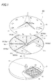
- FIG. 1 is an exploded perspective view of a timepiece 100 according to the present embodiment.
- the timepiece 100 of the present embodiment includes a dial plate 1, a module 3 including a circularly polarized antenna 4, and a solar panel 5.
- the dial plate 1, the module 3, the circularly polarized antenna 4, and the solar panel 5 are housed in a case (not shown).
- the dial plate 1 is disposed on the viewable side of the timepiece 100. And, the dial plate 1 is an analog type dial plate for displaying time by clock hands 2 such as an hour hand and a minute hand.
- a through-hole 11 for inserting a hand spindle 31 for fitting the clock hands 2 is formed.
- the timepiece 100 of the present embodiment includes the circularly polarized antenna 4 for receiving GPS electric waves which are microwaves, as described below. Therefore, it is preferable that the dial plate 1 is made of a non-magnetic material transmitting microwaves.
- the dial plate 1 can be made of, for example, a resin or glass.
- the timepiece 100 includes the solar panel 5 for receiving light and generating electric power. Therefore, the dial plate I is made of a transparent or semitransparent material having optical transparency.
- the dial plate 1 may be formed, for example, by depositing a metal film or by performing various printing on a surface of a base material.
- the base material can be made of a transparent or semitransparent material such that a resin or glass.
- the metal film is so thick that it does not attenuate microwaves and does not disturb light transmission.
- the module 3 is disposed below the dial plate 1 and the solar panel 5 (that is, on the rear side of the timepiece 100).
- the module 3 is formed, for example, to include a timepiece movement which is configured by a gear train mechanism, a motor, and the like for operating the clock hands 2, and a communication module which is connected to the circularly polarized antenna 4 (both of the timepiece movement and the communication module are not shown), inside a housing (not shown) made of a resin or the like.
- the module 3 is formed, for example, to include a secondary battery 6 which stores electric power generated by the solar panel 5, a circuit board 7 on which there are mounted various electronic components such as a control circuit for performing time display using the clock hands 2 (see FIG. 2 with respect to the secondary battery and the circuit board), and the like, inside a housing (not shown) made of a resin or the like.
- the hand spindle 31 in an approximately central portion of the module 3, is provided so as to protrude upward from the movement side.
- the hand spindle 31 is a spindle in which a plurality of rotating shafts for the hour hand, the minute hand, the second hand, and the like are arranged so as to overlap on the same axis.
- the hand spindle 31 is inserted into a through-hole 51 of the solar panel 5 (described below) and the through-hole 11 of the dial plate 1.
- the individual rotating shafts are connected respectively to the clock hands 2 (such that the hour hand, the minute hand, and the second hand) corresponding to the rotating shafts.
- the circularly polarized antenna 4 is arranged.
- the circularly polarized antenna 4 is arranged such that the center of the circularly polarized antenna 4 is in an area range from 4 o'clock to 7 o'clock through 6 o'clock on the dial plate 1 as seen in a plan view.
- the circularly polarized antenna 4 can receive GPS electric waves (that is, electric waves which are transmitted from GPS satellites and include time information and the like) which are microwaves which are circularly polarized waves.
- GPS electric waves that is, electric waves which are transmitted from GPS satellites and include time information and the like
- microwaves which are circularly polarized waves.
- a patch antenna can be preferably used.
- GPS electric waves include data including time information according to high-accuracy atomic clocks mounted in the individual GPS satellites, appropriately accurate ephemerides (that is, trajectory information) of all satellites which are updated about every 6 days, and ephemerides of the satellites which are updated every 90 minutes.
- the individual GPS satellites transmit the above information to the earth by electric waves (microwaves) with a frequency of L1 (1575.42 MHz) or L2 (1227.60 MHz).
- the timepiece 100 can receive a GPS electric wave from at least one of the plurality of GPS satellites by the circularly polarized antenna 4. And, The timepiece 100 can use the time information and the like included in the GPS electric wave to correct the internal time of the timepiece 100 to the exact time.
- GPS electric waves include trajectory information representing the positions of the individual GPS satellites on their trajectories as described above. Therefore, the timepiece 100 can also receive GPS electric waves transmitted respectively from the plurality of GPS satellites by the circularly polarized antenna 4, and use the time information, the trajectory information, and the like included in the GPS electric waves to perform positioning calculation.
- the circularly polarized antenna 4 of the present embodiment is formed in a rectangular shape as seen in a plan view.
- the circularly polarized antenna 4 includes a base 41 and a radiation electrode (radiation element) 42 disposed on the base 41.
- the shape of the circularly polarized antenna 4 is not limited to the illustrated example.
- the base 41 is made of a dielectric material such as ceramic.
- the radiation electrode 42 consists of, for example, silver foil, a metal plate, a metal film, or the like with a predetermined thickness.
- the size (the lengths of individual sides) of the radiation electrode 42 is optimized based on the frequency of electric waves which are received by the circularly polarized antenna 4, and the like.
- the size of the radiation electrode is adjusted such that the highest antenna characteristics are performed at the frequency band of the GPS electric waves.
- a power supply point 43 for supplying electric power to the radiation electrode 42 is provided.
- the method of supplying electric power to the radiation electrode 42 is not especially limited.
- a through-hole may be formed in the thickness direction of the circularly polarized antenna 4.
- a power supply member (not shown) for supplying electric power to the radiation electrode 42 is inserted into the through-hole.
- the power supply member might be a power supply pin or a coaxial cable, for example.
- the circularly polarized antenna 4 of the present embodiment is disposed in the module 3 while avoiding the hand spindle 31 (see FIG. 5 ).
- the position where the circularly polarized antenna 4 is provided is not limited to the illustrated example.
- the direction in which the circularly polarized antenna 4 is arranged is not limited to the illustrated example.
- a radiation pattern spreads from the peripheral portion (edge portion) of the radiation electrode 42.
- the radiation electrode 42 is formed substantially in a square shape.
- the radiation pattern spreading from each side (peripheral portion) has a big influence on the antenna characteristics of the circularly polarized antenna 4 (the electric wave reception performance of the antenna).
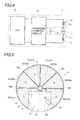
- FIG. 2 is a schematic side view illustrating an internal configuration of the module 3.
- the secondary battery 6 and the circuit board 7 described above are contained.
- the secondary battery 6 is disposed below the circuit board 7.
- the secondary battery 6 is electrically connected to the circuit board 7.
- the circuit board 7 electrically connects the secondary battery 6 and the solar panel 5.
- the circuit board 7 is electrically connected to the solar panel 5 disposed above the circuit board 7.
- a positive electrode 71p on the circuit board 7 is electrically connected to the solar panel 5 (a solar cell 50a to be described below) through a connector (a connection member) 81 p
- a negative electrode 71 n is electrically connected to the solar panel 5 (a solar cell 50f to be described below) through a connector (a connection member) 81n.
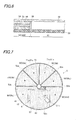
- FIG. 3 is a schematic block diagram illustrating a control configuration of the timepiece 100.
- FIG. 3 is for mainly explaining the power storing (charging) function of the timepiece 100.
- a central processing unit (CPU) 72 and a charging control circuit 73 are mounted on the circuit board 7.
- the central processing unit (CPU) 72 comprehensively controls individual units of the timepiece 100.
- the charging control circuit 73 controls an operation of charging the secondary battery 6 from the solar panel 5.
- the CPU 72 is electrically connected to the charging control circuit 73 and controls an operation of the charging control circuit 73. Also, the CPU 72 is electrically connected to the communication module, the timepiece movement, and the like (not shown) connected to the circularly polarized antenna 4. The CPU 72 performs time correction based on time information and the like included in GPS electric waves.
- the charging control circuit 73 is electrically connected to each of the solar panel 5 (a plurality of solar cells 50 to be described below) and the secondary battery 6, respectively.
- the charging control circuit 73 controls an operation of charging the secondary battery 6 from the solar panel 5, based on a control command from the CPU 72.
- an inductor 74 is electrically series-connected.
- This inductor 74 is a choke coil for reducing influence (noise) of a current generated from the solar panel 5 on GPS electric wave reception of the circularly polarized antenna 4.
- the inductor 74 has an inductance value of about 1 mH. More specifically, the inductor 74 is a circuit element which increases impedance (electric resistance) with respect to electric waves with the predetermined frequency which are received by the circularly polarized antenna 4 while having low electric resistance (in the present embodiment, DC resistance) with respect to a generated current from the solar panel 5.
- the position where the inductor 74 is provided is not especially limited as long as it is on the wiring route between the solar panel 5 and the secondary battery 6. It is preferable that the position of the inductor 74 may be a position close to the solar panel 5. In order to suppress superposition of a high-frequency current on a circuit, it is more preferable that the position of the inductor 74 may be an intermediate position on a wiring route having a larger route length (conductor length).
- the inductor 74 may be provided on a wiring route on the negative electrode (71n) side, not on the positive electrode (71p) side, and it is more preferable that two inductors 74 may be provided respectively on the positive electrode (71p) side and the negative electrode (71n) side as shown in FIG. 4 .
- the solar panel 5 receives light and generates electric power.
- the electric power generated by the solar panel 5 is stored in the secondary battery 6.
- the solar panel 5 of the present embodiment is disposed between the dial plate 1 and the module 3, and has an area corresponding to the area of the planar direction of the dial plate 1.
- the dial plate 1 of the present embodiment is made of a material having optical transparency as described above.
- the area of the solar panel 5 corresponds to the area of the planar direction of the dial plate 1. Therefore, it is possible to maximally secure a light reception area of the solar panel 5.
- the shape and the like of the solar panel 5 are not especially limited.
- the solar panel 5 needs only to have an area substantially corresponding to the area of the planar direction of the dial plate 1 and substantially overlap the dial plate 1.
- the area and shape of the solar panel 5 may not coincide with the area and shape of the dial plate 1.
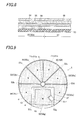
- FIG. 5 is a plan view of the solar panel 5 according to the present embodiment
- FIG. 6 is a cross-sectional view of the solar panel 5 along a line VI-VI of FIG. 5 .
- the through-hole 51 for inserting the hand spindle 31 is formed.
- the solar panel 5 includes not only the plurality of solar cells 50 (in the present embodiment, six solar cells 50a to 50f) which is light receiving sections, but also a non-power generation section 57 disposed at a position corresponding to the radiation electrode 42 of the circularly polarized antenna 4.
- the position corresponding to the radiation electrode 42 is a position above the radiation electrode 42.
- the circularly polarized antenna 4 has the radiation pattern spreading from the peripheral portion of the radiation electrode 42, if the peripheral portion of the radiation electrode 42 is covered by a member inhibiting transmission of electric waves, the antenna characteristics (electric wave reception performance) deteriorates.
- a portion of the solar panel 5 which is to be positioned above the radiation electrode 42 consists of the non-power generation section 57 which is made of only a non-conductive material, without containing conductive materials so as not to perform light reception and power generation.
- the size of the non-power generation section 57 may be slightly larger than the size of the radiation electrode 42.
- the non-power generation section 57 is formed such that each width of the non-power generation section 57 is larger than each width of the radiation electrode 42 by 2 mm approximately all over the circumference.
- the solar panel 5 has a structure in which metal electrodes 54, a semiconductor layer 55, and transparent electrodes 56 are sequentially stacked on a resin substrate 53 to constitute the individual solar cells 50.
- a protective layer (protective film) 58 is stacked on the transparent electrodes 56.
- an insulating layer 59 is disposed on the side surfaces of the laminate structures composed of the metal electrodes 54, the semiconductor layer 55, and the transparent electrodes 56 to constitute the individual solar cells 50.
- the resin substrate 53 is a flexible film-like substrate.
- the material which forms the resin substrate 53 is not especially limited.
- the resin substrate 53 may be made of, for example, plastic.
- the metal electrodes 54 are made of a material containing a metal material such as an aluminum conductor. Also, the material which forms the metal electrodes 54 is not limited thereto.
- the semiconductor layer 55 is made of, for example, amorphous silicon (a-Si:H).
- a-Si:H amorphous silicon
- As the semiconductor layer 55 for example, a p-n junction type semiconductor having a junction between a p-type semiconductor and an n-type semiconductor can be used.
- the metal electrodes 54 and the semiconductor layer 55 are stacked on the resin substrate 53 by a method such as deposition. Also, the method of forming the metal electrodes 54 and the semiconductor layer 55 on the resin substrate 53 is not limited thereto.
- the transparent electrodes 56 are formed by crystallizing, for example, zinc oxide, indium oxide, or tin oxide on a substrate such as glass. Also, the material and formation method of the transparent electrodes 56 are not limited thereto.
- the non-power generation section 57 of the solar panel 5 is formed by removing the metal electrodes 54, the semiconductor layer 55, and the transparent electrodes 56 which are portions to be positioned above the radiation electrode 42.
- the method of removing the metal electrodes 54, the semiconductor layer 55, and the transparent electrodes 56 is not especially limited. For example, laser processing can be used. Also, instead of removing the metal electrodes 54, the semiconductor layer 55, and the transparent electrodes 56 stacked, the metal electrodes 54, the semiconductor layer 55, and the transparent electrodes 56 may be stacked while avoiding the portion where the non-power generation section 57 will be provided (that is, the portion to be positioned above the radiation electrode 42).
- the six solar cells 50a to 50f are formed so as to have approximately equal areas as shown in FIGS. 1 and 5 such that the output currents of the individual solar cells become substantially equal.
- the solar cells 50a to 50f are connected in series, and functions as one solar panel.
- the solar cell 50a is electrically connected to the neighboring solar cell 50b at a connection portion 52a
- the solar cell 50b is electrically connected to the neighboring solar cell 50c at a connection portion 52b
- the solar cells 50c to 50e are electrically connected to the neighboring solar cells 50d to 50f at connection portions 52c to 52e.
- the solar cell 50a is electrically connected to the positive electrode 71p on the circuit board 7, through the connector 81 p.
- the solar cell 50f is electrically connected to the negative electrode 71n on the circuit board 7, through the connector 81 n (see FIG. 2 ).
- the six solar cells 50a to 50f are electrically connected to the circuit board 7 in a state where they are connected in series.
- connection positions where the solar panel 5 and the circuit board 7 are electrically connected that is, the positions of the two electrodes 71p and 71n of the circuit board 7 or the two connectors 81p and 81 n are not especially limited as long as the six solar cells 50a to 50f are connected in series while being electrically connected to the circuit board 7, and may be, for example, on the solar cell 50c and the solar cell 50d.
- connection positions may be positions apart from the circularly polarized antenna 4 like in the present embodiment. Specifically, in a case of defining a boundary line as a line passing through the center of the solar panel 5 while being perpendicular to a line connecting the center of the circularly polarized antenna 4 and the center of the solar panel 5, it is preferable that, as seen in a plan view of the solar panel, the connection positions may be provided in the opposite area (the upper half area of FIG. 5 ) to an area (the lower half area of FIG. 5 ) where the circularly polarized antenna 4 is provided across the boundary line, in the solar panel 5.
- the circularly polarized antenna 4 is positioned as described above such that the center is in the area range from 4 o'clock to 7 o'clock through 6 o'clock on the dial plate 1 as seen in a plan view, it is more preferable that the corresponding connection positions may be in an area range from 8 o'clock to 12 o'clock through 2 o'clock on the dial plate 1 (see FIG. 1 ). Also, the circularly polarized antenna 4 is positioned while avoiding the center of the solar panel 5 in this case.
- connection positions of the solar panel 5 and the circuit board 7 are spaced apart from the circularly polarized antenna 4, conductive materials (such as the two electrodes 71 p and 71 n or the two connectors 81p and 81 n) which are provided at the connection positions are disposed at positions apart from the circularly polarized antenna 4. Therefore, the impedance of the solar panel 5 around the position above the circularly polarized antenna 4 becomes higher than the impedance of the solar panel 5 in the vicinities of the connection positions apart from the circularly polarized antenna 4.
- a date wheel (not shown) is disposed in the module 3, and a date display window 12 for displaying date is formed in the dial plate 1.
- a date display opening 511 is formed.
- the date display opening 511 is formed in the non-power generation section 57 which is a part of the solar panel 5 and does not perform light reception and power generation.
- the timepiece 100 of the present embodiment if light passing through the dial plate 1 from the viewable side enters the solar panel 5 having the solar cells 50a to 50f the light enters the semiconductor layer 55 through the transparent electrodes 56. If the light enters the semiconductor layer 55, electrons and holes are generated around the junction between the p-type semiconductor and the n-type semiconductor. The generated electrons and holes move toward the n-type semiconductor and the p-type semiconductor, respectively, whereby an electromotive force (photoelectromotive force) is generated. As a result, current flows in circuits connected to the transparent electrodes 56 and the metal electrodes 54. Electric power generated in this way by the solar panel 5 is stored in the secondary battery 6 through the circuit board 7.
- the inductor 74 provided on the wiring route on the circuit board 7 from the solar panel 5 to the secondary battery 6 has electric resistance of almost 0 ⁇ to the generated current (DC current) from the solar panel 5, and thus does not block the generated current.
- electric power generated by the solar panel 5 is appropriately stored in the secondary battery 6.
- the CPU 72 on the circuit board 7 corrects the internal time of the timepiece 100 to the exact time, based on time information and the like included in the GPS electric waves received by the circularly polarized antenna 4.
- f is the frequency of a signal
- L is the inductance value of the circuit. Since the frequency of the GPS electric waves is about 1.5 GHz as described above, and the inductance value of the inductor 74 is about 1 mH as described above, from the above expression, the impedance Z of the corresponding charging circuit at the frequency of the GPS electric waves becomes about 10 k ⁇ .
- the peripheral portion of the radiation electrode 42 of the circularly polarized antenna 4 is covered by the conductive materials (such as the metal electrodes 54, the semiconductor layer 55, and the transparent electrodes 56 of the solar cells 50), spreading of the radiation pattern is not inhibited, and the circularly polarized antenna 4 can appropriately receive GPS electric waves.
- the inductor 74 is provided so as to have low DC resistance to a generated current from the solar panel 5 while increasing impedance to electric waves which are received by the circularly polarized antenna 4.
- connection positions where the solar panel 5 and the circuit board 7 are electrically connected are positions apart from the circularly polarized antenna 4. That is, in a case of defining a boundary line as a line passing through the center of the solar panel 5 while being perpendicular to a line connecting the center of the circularly polarized antenna 4 and the center of the solar panel 5, as seen in a plan view, the connection positions are provided in the opposite area of the corresponding boundary line to the area where the circularly polarized antenna 4 is provided, in the solar panel 5.
- the conductive materials (such as the two electrodes 71p and 71n or the two connectors 81p and 81 n) which are provided at the connection positions are disposed at positions apart from the circularly polarized antenna 4, and the impedance of the solar panel 5 around the position above the circularly polarized antenna 4 becomes higher than the impedance of the solar panel 5 in the vicinities of the connection positions apart from the circularly polarized antenna 4. Therefore, it is possible to further reduce a bad influence of the conductive materials of the solar panel 5 on GPS electric wave reception of the circularly polarized antenna 4.
- the circularly polarized antenna 4 is disposed below the solar panel 5, and the solar panel 5 has the non-power generation section 57 made of a non-conductive material at the position corresponding to the radiation electrode 42 of the circularly polarized antenna 4.
- the peripheral portion of the radiation electrode 42 is not covered by a conductive material. Therefore, it is possible to suppress deterioration of the antenna characteristics of the circularly polarized antenna 4, and appropriately receive GPS electric waves.
- the inductor 74 which is a choke coil having an inductance value of about 1 mH is provided.
- the circuit element is not limited thereto, and may be a choke coil having any other inductance value, or may be any other EMC countermeasure component such as a filter.
- the non-power generation section 57 which is provided at the position of the solar panel 5 corresponding to the radiation electrode 42 consists of the non-conductive material remaining by removing the conductive materials (the metal electrodes 54 and the transparent electrodes 56) and the like.
- an opening (a portion where the resin substrate 53 and the protective layer 58 do not exist) is formed at the position corresponding to the radiation electrode 42.
- the non-power generation section 57 of the solar panel 5 may be formed by removing only the metal electrodes 54 as shown in FIGS. 7 and 8 .
- FIG. 7 is a plan view illustrating a modification of the solar panel 5
- FIG. 8 is a cross-sectional view along a line VIII-VIII of FIG. 7 .
- the non-power generation section 57 may be provided by removing only the metal electrodes 54, such that it has the semiconductor layer 55 and the transparent electrodes 56 like the solar cells 50.
- the transparent electrodes 56 is configured by a conductive material, since the electrical conductivity of the transparent electrodes 56 is lower than the metal electrodes 54 which is configured by an aluminum conductor or the like, a bad influence on the antenna characteristics of the circularly polarized antenna 4 is relatively small.
- the non-power generation section 57 has the transparent electrodes 56 and the semiconductor layer 55 positioned on the front side, like the solar cells 50, when the timepiece 100 is viewed from the dial plate (1) side, the solar cells 50 and the non-power generation section 57 look the same.
- the non-power generation section 57 is configured by removing only the metal electrodes 54, it is possible to suppress deterioration of the antenna characteristics of the circularly polarized antenna 4 while improving designability.
- the non-power generation section 57 of the solar panel 5 may be provided at a position corresponding to the peripheral portion of the radiation electrode 42 as shown in FIG. 9 .
- FIG. 9 is a plan view illustrating another modification of the solar panel 5.
- the non-power generation section 57 may be provided in an annular shape only at a position corresponding to the peripheral portion of the radiation electrode 42 of the circularly polarized antenna 4, not over the entire radiation electrode 42.
- the non-power generation section 57 may be formed by removing only the metal electrodes 54 like in the above described modification.
- an addition solar cell 50 (a solar cell 50g) is provided on the inner side from the non-power generation section 57 (an area surrounded by the non-power generation section 57), it is possible to secure a wider light receiving section of the solar panel 5, thereby improving power generation capacity. Also, in this case, it goes without saying that the added solar cell 50g is electrically connected in series to the other solar cells 50a to 50f (for example, by connection portions 52c and 52g in FIG. 9 ) and is formed so as to have an area substantially equal to those of the other solar cells 50a to 50f.
- the non-power generation section 57 is provided at a position corresponding to the peripheral portion of the radiation electrode 42, it is possible to suppress deterioration of the antenna characteristics of the circularly polarized antenna 4 while improving the power generation capacity of the solar panel 5.
- the division method of the solar panel (such as the number of partitions and the shape of each divided solar cell) is not limited to that exemplified in the above described embodiment.
- the antenna according to the present invention is not limited to a circularly polarized antenna for receiving GPS electric waves, and needs only to be an antenna able to receive electric waves with a predetermined frequency, such as an antenna corresponding to Bluetooth (a registered trademark) or any other high-frequency wireless communication.
- the timepiece which is the electronic device is the analog type timepiece 100 which rotates the clock hands 2 on the dial plate 1, thereby displaying time and the like has been exemplified.
- the timepiece is not limited to the analog type timepiece.
- the timepiece may be, for example, a digital type timepiece having a dial plate (such as a liquid crystal display unit) for displaying various information such as time and calendar information by characters and the like. Also, a dial plate having both of an analog type display unit and a digital type display unit may be included in the electronic device.
- a dial plate such as a liquid crystal display unit
- a dial plate having both of an analog type display unit and a digital type display unit may be included in the electronic device.
- the electronic device according to the present invention is a timepiece (electronic timepiece) has been exemplified.
- the corresponding electronic device is not limited thereto.
- the electronic device needs only to perform photovoltaic power generation by a solar panel, store the generated electric power in a secondary battery, and receive electric waves with a predetermined frequency by an antenna disposed near the solar panel, and may be, for example, a biological information display such as a pedometer, a heart rate meter, or a pulsimeter, or a display for displaying various information such as movement distance and movement pace information, altitude information, and air pressure information.
- a biological information display such as a pedometer, a heart rate meter, or a pulsimeter
- a display for displaying various information such as movement distance and movement pace information, altitude information, and air pressure information.
Landscapes
- Physics & Mathematics (AREA)
- General Physics & Mathematics (AREA)
- Engineering & Computer Science (AREA)
- Power Engineering (AREA)
- Electric Clocks (AREA)
- Electromechanical Clocks (AREA)
- Photovoltaic Devices (AREA)
Applications Claiming Priority (1)
| Application Number | Priority Date | Filing Date | Title |
|---|---|---|---|
| JP2014133744A JP6119683B2 (ja) | 2014-06-30 | 2014-06-30 | 電子機器 |
Publications (2)
| Publication Number | Publication Date |
|---|---|
| EP2963508A2 true EP2963508A2 (de) | 2016-01-06 |
| EP2963508A3 EP2963508A3 (de) | 2016-03-16 |
Family
ID=53373332
Family Applications (1)
| Application Number | Title | Priority Date | Filing Date |
|---|---|---|---|
| EP15171294.0A Ceased EP2963508A3 (de) | 2014-06-30 | 2015-06-10 | Elektronische vorrichtung |
Country Status (4)
| Country | Link |
|---|---|
| US (1) | US20150378313A1 (de) |
| EP (1) | EP2963508A3 (de) |
| JP (1) | JP6119683B2 (de) |
| CN (1) | CN105319947B (de) |
Families Citing this family (12)
| Publication number | Priority date | Publication date | Assignee | Title |
|---|---|---|---|---|
| US20170023612A1 (en) * | 2015-07-22 | 2017-01-26 | Iometers, LLC | Meter Box Lid |
| CN105974783B (zh) * | 2016-06-16 | 2019-03-05 | 浙江卓越电子有限公司 | 一种智能手表机芯结构 |
| CN105974784B (zh) * | 2016-06-16 | 2019-03-05 | 浙江卓越电子有限公司 | 一种抗震动的手表机芯结构 |
| US20180034325A1 (en) | 2016-06-20 | 2018-02-01 | AMI Research & Development, LLC | Low frequency rectenna system for wireless charging |
| US10732578B2 (en) * | 2016-11-08 | 2020-08-04 | Seiko Epson Corporation | Electronic timepiece |
| JP6874453B2 (ja) * | 2017-03-21 | 2021-05-19 | セイコーエプソン株式会社 | 電子時計 |
| JP2019032221A (ja) * | 2017-08-08 | 2019-02-28 | セイコーエプソン株式会社 | 携帯型電子機器 |
| JP7098946B2 (ja) * | 2018-02-01 | 2022-07-12 | セイコーエプソン株式会社 | 太陽電池付ムーブメントおよび時計 |
| JP7073833B2 (ja) * | 2018-03-23 | 2022-05-24 | セイコーエプソン株式会社 | 電子時計 |
| JP7151453B2 (ja) | 2018-12-18 | 2022-10-12 | セイコーエプソン株式会社 | 電子時計 |
| JP7078024B2 (ja) * | 2019-10-15 | 2022-05-31 | カシオ計算機株式会社 | ソーラーパネル、電子機器及び電子時計 |
| JP7310553B2 (ja) * | 2019-11-06 | 2023-07-19 | セイコーエプソン株式会社 | 電子時計 |
Citations (2)
| Publication number | Priority date | Publication date | Assignee | Title |
|---|---|---|---|---|
| JP2010066151A (ja) | 2008-09-11 | 2010-03-25 | Seiko Epson Corp | リスト機器 |
| WO2011081630A1 (en) * | 2009-12-30 | 2011-07-07 | Rayspan Corporation | Antenna devices having frequency-dependent connection to electrical ground |
Family Cites Families (16)
| Publication number | Priority date | Publication date | Assignee | Title |
|---|---|---|---|---|
| US5027051A (en) * | 1990-02-20 | 1991-06-25 | Donald Lafferty | Photovoltaic source switching regulator with maximum power transfer efficiency without voltage change |
| JP4215402B2 (ja) * | 1998-11-10 | 2009-01-28 | シチズンホールディングス株式会社 | 太陽電池付き電子機器 |
| CN1161674C (zh) * | 1998-11-26 | 2004-08-11 | 时至准钟表股份有限公司 | 带有太阳电池的钟表 |
| JP3925552B2 (ja) * | 2003-05-09 | 2007-06-06 | セイコーエプソン株式会社 | 無線通信機能付電子時計 |
| JP2007187504A (ja) * | 2006-01-12 | 2007-07-26 | Seiko Instruments Inc | デジタル表示式電波修正時計及び該時計の標準電波受信方法 |
| JP5307105B2 (ja) * | 2010-01-06 | 2013-10-02 | 株式会社神戸製鋼所 | 複合型巻線素子ならびにこれを用いた変圧器、変圧システムおよびノイズカットフィルタ用複合型巻線素子 |
| JP2011208948A (ja) * | 2010-03-26 | 2011-10-20 | Citizen Holdings Co Ltd | 電波腕時計 |
| JP5531830B2 (ja) * | 2010-07-05 | 2014-06-25 | セイコーエプソン株式会社 | 電子時計 |
| KR101678222B1 (ko) * | 2010-09-30 | 2016-11-21 | 삼성전자주식회사 | 키패드를 구비한 휴대용 단말기 |
| JP5598257B2 (ja) * | 2010-10-28 | 2014-10-01 | カシオ計算機株式会社 | 電子機器 |
| JP5866860B2 (ja) * | 2011-01-05 | 2016-02-24 | セイコーエプソン株式会社 | 無線機能付き時計 |
| JP5742349B2 (ja) * | 2011-03-23 | 2015-07-01 | セイコーエプソン株式会社 | アンテナ装置および電子機器 |
| CN202587606U (zh) * | 2012-05-30 | 2012-12-05 | 江苏伟信电子有限公司 | 一种用于手机天线的fpc |
| JP5962252B2 (ja) * | 2012-06-25 | 2016-08-03 | セイコーエプソン株式会社 | 太陽電池付電子時計 |
| CN103078172B (zh) * | 2013-02-20 | 2015-03-25 | 上海安费诺永亿通讯电子有限公司 | 具有高敏感度感应装置的天线 |
| US10039492B2 (en) * | 2014-06-13 | 2018-08-07 | Verily Life Sciences, LLC | Conditional storage |
-
2014
- 2014-06-30 JP JP2014133744A patent/JP6119683B2/ja active Active
-
2015
- 2015-06-03 US US14/729,414 patent/US20150378313A1/en not_active Abandoned
- 2015-06-10 EP EP15171294.0A patent/EP2963508A3/de not_active Ceased
- 2015-06-19 CN CN201510347401.9A patent/CN105319947B/zh active Active
Patent Citations (2)
| Publication number | Priority date | Publication date | Assignee | Title |
|---|---|---|---|---|
| JP2010066151A (ja) | 2008-09-11 | 2010-03-25 | Seiko Epson Corp | リスト機器 |
| WO2011081630A1 (en) * | 2009-12-30 | 2011-07-07 | Rayspan Corporation | Antenna devices having frequency-dependent connection to electrical ground |
Also Published As
| Publication number | Publication date |
|---|---|
| JP2016011897A (ja) | 2016-01-21 |
| JP6119683B2 (ja) | 2017-04-26 |
| US20150378313A1 (en) | 2015-12-31 |
| CN105319947A (zh) | 2016-02-10 |
| CN105319947B (zh) | 2019-04-30 |
| EP2963508A3 (de) | 2016-03-16 |
Similar Documents
| Publication | Publication Date | Title |
|---|---|---|
| EP2963508A2 (de) | Elektronische vorrichtung | |
| JP6428823B2 (ja) | 電子機器 | |
| US9823625B2 (en) | Electronic device | |
| CN102467085B (zh) | 具备天线装置和太阳能电池板的手表 | |
| CN104950664B (zh) | 具备太阳能面板的电子设备 | |
| JP6696195B2 (ja) | 電子時計 | |
| US8482470B2 (en) | Electric device with an antenna device and a solar panel | |
| JP6488548B2 (ja) | 電子機器 | |
| JP7107089B2 (ja) | 電子時計 | |
| US11537083B2 (en) | Electronic timepiece | |
| JP6575588B2 (ja) | ソーラーパネル、および電子機器 | |
| JP6264987B2 (ja) | 電子機器 | |
| JP5742349B2 (ja) | アンテナ装置および電子機器 | |
| JP2019191146A (ja) | 電子時計 | |
| CN112671327A (zh) | 太阳电池板、电子设备以及电子钟表 | |
| CN112213935B (zh) | 钟表 | |
| HK1236055A1 (en) | Electronic device |
Legal Events
| Date | Code | Title | Description |
|---|---|---|---|
| PUAI | Public reference made under article 153(3) epc to a published international application that has entered the european phase |
Free format text: ORIGINAL CODE: 0009012 |
|
| 17P | Request for examination filed |
Effective date: 20150610 |
|
| AK | Designated contracting states |
Kind code of ref document: A2 Designated state(s): AL AT BE BG CH CY CZ DE DK EE ES FI FR GB GR HR HU IE IS IT LI LT LU LV MC MK MT NL NO PL PT RO RS SE SI SK SM TR |
|
| AX | Request for extension of the european patent |
Extension state: BA ME |
|
| PUAL | Search report despatched |
Free format text: ORIGINAL CODE: 0009013 |
|
| AK | Designated contracting states |
Kind code of ref document: A3 Designated state(s): AL AT BE BG CH CY CZ DE DK EE ES FI FR GB GR HR HU IE IS IT LI LT LU LV MC MK MT NL NO PL PT RO RS SE SI SK SM TR |
|
| AX | Request for extension of the european patent |
Extension state: BA ME |
|
| RIC1 | Information provided on ipc code assigned before grant |
Ipc: G04C 10/02 20060101ALI20160208BHEP Ipc: G04R 60/10 20130101AFI20160208BHEP |
|
| STAA | Information on the status of an ep patent application or granted ep patent |
Free format text: STATUS: THE APPLICATION HAS BEEN REFUSED |
|
| 18R | Application refused |
Effective date: 20200206 |