EP2963508A2 - Electronic device - Google Patents
Electronic device Download PDFInfo
- Publication number
- EP2963508A2 EP2963508A2 EP15171294.0A EP15171294A EP2963508A2 EP 2963508 A2 EP2963508 A2 EP 2963508A2 EP 15171294 A EP15171294 A EP 15171294A EP 2963508 A2 EP2963508 A2 EP 2963508A2
- Authority
- EP
- European Patent Office
- Prior art keywords
- solar panel
- antenna
- circularly polarized
- secondary battery
- circuit board
- Prior art date
- Legal status (The legal status is an assumption and is not a legal conclusion. Google has not performed a legal analysis and makes no representation as to the accuracy of the status listed.)
- Ceased
Links
Images

Classifications
-
- G—PHYSICS
- G04—HOROLOGY
- G04C—ELECTROMECHANICAL CLOCKS OR WATCHES
- G04C10/00—Arrangements of electric power supplies in time pieces
- G04C10/02—Arrangements of electric power supplies in time pieces the power supply being a radioactive or photovoltaic source
-
- G—PHYSICS
- G04—HOROLOGY
- G04R—RADIO-CONTROLLED TIME-PIECES
- G04R60/00—Constructional details
- G04R60/06—Antennas attached to or integrated in clock or watch bodies
- G04R60/10—Antennas attached to or integrated in clock or watch bodies inside cases
Landscapes
- Physics & Mathematics (AREA)
- General Physics & Mathematics (AREA)
- Engineering & Computer Science (AREA)
- Power Engineering (AREA)
- Electric Clocks (AREA)
- Electromechanical Clocks (AREA)
- Photovoltaic Devices (AREA)
Abstract
Description
- The present invention relates to an electronic device.
- For example,
JP-A-2010-066151 - However, since the above described configuration needs a dedicated switching element for a control circuit and should perform troublesome switching control according to an electric wave reception state, the configuration is complicated.
- Further, since it is impossible to store electric power generated by the solar panel in the secondary battery during electric wave reception, the power storage amount (charge amount) of the secondary battery decreases that much.
- The present invention is an electronic device having a simple configuration, capable of appropriately performing reception of electric waves with a predetermined frequency and capable of storage of electric power in a secondary battery.
- In order to solve the above described problems, an electronic device according to the present invention includes a solar panel, a secondary battery, an antenna and a circuit board. The solar panel receives light to generate electric power. The secondary battery stores electric power generated by the solar panel. The antenna is disposed near the solar panel and receives electric waves with a predetermined frequency. The circuit board electrically connects the solar panel and the secondary battery. On a wiring route which is formed on the circuit board so as to electrically connect the solar panel and the secondary battery, at least one circuit element is provided so as to have high electric resistance with respect to electric waves which are received by the antenna while having low electric resistance with respect to a generated current from the solar panel.
-
-
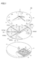
FIG. 1 is an exploded perspective view of a timepiece according to an embodiment. -
FIG. 2 is a schematic side view illustrating an internal configuration of a module according to the embodiment. -
FIG. 3 is a schematic block diagram illustrating a control configuration of the timepiece according to the embodiment. -
FIG. 4 is a schematic block diagram illustrating a modification of the control configuration of the timepiece according to the embodiment. -
FIG. 5 is a plan view of a solar panel according to the embodiment. -
FIG. 6 is a cross-sectional view of the solar panel along a line VI-VI ofFIG. 5 . -
FIG. 7 is a plan view illustrating a modification of the solar panel according to the embodiment. -
FIG. 8 is a cross-sectional view of the modification of the solar panel along a line VIII-VIII ofFIG 7 . -
FIG. 9 is a plan view illustrating another modification of the solar panel according to the embodiment. - Embodiments of an electronic device according to the present invention will be described with reference to
FIGS. 1 to 6 . - Additionally, although the after-mentioned embodiments are provided with various technically preferred limitations to perform the present invention, the scope of the present invention is not limited to the following embodiments and illustrated examples.
- In the present embodiment, a case where the electronic device is an analog type timepiece (electronic timepiece) which operates clock hands, thereby displaying time and the like.
-
FIG. 1 is an exploded perspective view of atimepiece 100 according to the present embodiment. - As shown in
FIG. 1 , thetimepiece 100 of the present embodiment includes adial plate 1, amodule 3 including a circularly polarizedantenna 4, and asolar panel 5. - The
dial plate 1, themodule 3, the circularly polarizedantenna 4, and thesolar panel 5 are housed in a case (not shown). - In the present embodiment, the
dial plate 1 is disposed on the viewable side of thetimepiece 100. And, thedial plate 1 is an analog type dial plate for displaying time byclock hands 2 such as an hour hand and a minute hand. - In an approximately central portion of the
dial plate 1, a through-hole 11 for inserting ahand spindle 31 for fitting theclock hands 2 is formed. - The
timepiece 100 of the present embodiment includes the circularly polarizedantenna 4 for receiving GPS electric waves which are microwaves, as described below. Therefore, it is preferable that thedial plate 1 is made of a non-magnetic material transmitting microwaves. Thedial plate 1 can be made of, for example, a resin or glass. - Further, the
timepiece 100 includes thesolar panel 5 for receiving light and generating electric power. Therefore, the dial plate I is made of a transparent or semitransparent material having optical transparency. - The
dial plate 1 may be formed, for example, by depositing a metal film or by performing various printing on a surface of a base material. The base material can be made of a transparent or semitransparent material such that a resin or glass. The metal film is so thick that it does not attenuate microwaves and does not disturb light transmission. - The
module 3 is disposed below thedial plate 1 and the solar panel 5 (that is, on the rear side of the timepiece 100). Themodule 3 is formed, for example, to include a timepiece movement which is configured by a gear train mechanism, a motor, and the like for operating theclock hands 2, and a communication module which is connected to the circularly polarized antenna 4 (both of the timepiece movement and the communication module are not shown), inside a housing (not shown) made of a resin or the like. Further, themodule 3 is formed, for example, to include asecondary battery 6 which stores electric power generated by thesolar panel 5, acircuit board 7 on which there are mounted various electronic components such as a control circuit for performing time display using the clock hands 2 (seeFIG. 2 with respect to the secondary battery and the circuit board), and the like, inside a housing (not shown) made of a resin or the like. - In the present embodiment, in an approximately central portion of the
module 3, thehand spindle 31 is provided so as to protrude upward from the movement side. - The
hand spindle 31 is a spindle in which a plurality of rotating shafts for the hour hand, the minute hand, the second hand, and the like are arranged so as to overlap on the same axis. Thehand spindle 31 is inserted into a through-hole 51 of the solar panel 5 (described below) and the through-hole 11 of thedial plate 1. The individual rotating shafts are connected respectively to the clock hands 2 (such that the hour hand, the minute hand, and the second hand) corresponding to the rotating shafts. - When the
hand spindle 31 rotates according to an operation of the movement, thevarious clock hands 2 which are fit on the individual rotating shafts of thehand spindle 31 individually rotate around thehand spindle 31 over the upper surface of thedial plate 1. - Also, in an end portion of the
module 3 along the outer periphery of the module, the circularly polarizedantenna 4 is arranged. - It is preferable that the circularly polarized
antenna 4 is arranged such that the center of the circularly polarizedantenna 4 is in an area range from 4 o'clock to 7 o'clock through 6 o'clock on thedial plate 1 as seen in a plan view. - The circularly polarized
antenna 4 can receive GPS electric waves (that is, electric waves which are transmitted from GPS satellites and include time information and the like) which are microwaves which are circularly polarized waves. For example, a patch antenna can be preferably used. - GPS electric waves include data including time information according to high-accuracy atomic clocks mounted in the individual GPS satellites, appropriately accurate ephemerides (that is, trajectory information) of all satellites which are updated about every 6 days, and ephemerides of the satellites which are updated every 90 minutes. The individual GPS satellites transmit the above information to the earth by electric waves (microwaves) with a frequency of L1 (1575.42 MHz) or L2 (1227.60 MHz).
- The
timepiece 100 can receive a GPS electric wave from at least one of the plurality of GPS satellites by the circularly polarizedantenna 4. And, Thetimepiece 100 can use the time information and the like included in the GPS electric wave to correct the internal time of thetimepiece 100 to the exact time. - Also, GPS electric waves include trajectory information representing the positions of the individual GPS satellites on their trajectories as described above. Therefore, the
timepiece 100 can also receive GPS electric waves transmitted respectively from the plurality of GPS satellites by the circularly polarizedantenna 4, and use the time information, the trajectory information, and the like included in the GPS electric waves to perform positioning calculation. - As shown in
FIG. 1 , the circularly polarizedantenna 4 of the present embodiment is formed in a rectangular shape as seen in a plan view. the circularly polarizedantenna 4 includes abase 41 and a radiation electrode (radiation element) 42 disposed on thebase 41. Also, the shape of the circularly polarizedantenna 4 is not limited to the illustrated example. - The
base 41 is made of a dielectric material such as ceramic. - The
radiation electrode 42 consists of, for example, silver foil, a metal plate, a metal film, or the like with a predetermined thickness. - The size (the lengths of individual sides) of the
radiation electrode 42 is optimized based on the frequency of electric waves which are received by the circularly polarizedantenna 4, and the like. In the present embodiment, the size of the radiation electrode is adjusted such that the highest antenna characteristics are performed at the frequency band of the GPS electric waves. - Also, in the circularly polarized
antenna 4, at a position having circular polarization characteristics, that is, at a position where impedance matching can be carried out, apower supply point 43 for supplying electric power to theradiation electrode 42 is provided. - Also, the method of supplying electric power to the
radiation electrode 42 is not especially limited. - Also, at a position corresponding to the
feeding point 43, a through-hole (not shown) may be formed in the thickness direction of the circularlypolarized antenna 4. A power supply member (not shown) for supplying electric power to theradiation electrode 42 is inserted into the through-hole. The power supply member might be a power supply pin or a coaxial cable, for example. - The circularly polarized
antenna 4 of the present embodiment is disposed in themodule 3 while avoiding the hand spindle 31 (seeFIG. 5 ). The position where the circularly polarizedantenna 4 is provided is not limited to the illustrated example. And the direction in which the circularlypolarized antenna 4 is arranged is not limited to the illustrated example. - In the circularly polarized
antenna 4, a radiation pattern spreads from the peripheral portion (edge portion) of theradiation electrode 42. - In the present embodiment, the
radiation electrode 42 is formed substantially in a square shape. The radiation pattern spreading from each side (peripheral portion) has a big influence on the antenna characteristics of the circularly polarized antenna 4 (the electric wave reception performance of the antenna). - Therefore, in order to improve the antenna characteristics of the circularly
polarized antenna 4, it is important not to prevent spreading of the radiation pattern from the peripheral portion of theradiation electrode 42. -
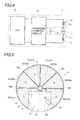
FIG. 2 is a schematic side view illustrating an internal configuration of themodule 3. - As shown in
FIG. 2 , inside themodule 3, thesecondary battery 6 and thecircuit board 7 described above are contained. - The
secondary battery 6 is disposed below thecircuit board 7. Thesecondary battery 6 is electrically connected to thecircuit board 7. - The
circuit board 7 electrically connects thesecondary battery 6 and thesolar panel 5. Thecircuit board 7 is electrically connected to thesolar panel 5 disposed above thecircuit board 7. Specifically, apositive electrode 71p on thecircuit board 7 is electrically connected to the solar panel 5 (asolar cell 50a to be described below) through a connector (a connection member) 81 p, and anegative electrode 71 n is electrically connected to the solar panel 5 (asolar cell 50f to be described below) through a connector (a connection member) 81n. -
FIG. 3 is a schematic block diagram illustrating a control configuration of thetimepiece 100.FIG. 3 is for mainly explaining the power storing (charging) function of thetimepiece 100. - As shown in
FIG. 3 , a central processing unit (CPU) 72 and a chargingcontrol circuit 73 are mounted on thecircuit board 7. The central processing unit (CPU) 72 comprehensively controls individual units of thetimepiece 100. The chargingcontrol circuit 73 controls an operation of charging thesecondary battery 6 from thesolar panel 5. - The
CPU 72 is electrically connected to the chargingcontrol circuit 73 and controls an operation of the chargingcontrol circuit 73. Also, theCPU 72 is electrically connected to the communication module, the timepiece movement, and the like (not shown) connected to the circularly polarizedantenna 4. TheCPU 72 performs time correction based on time information and the like included in GPS electric waves. - The charging
control circuit 73 is electrically connected to each of the solar panel 5 (a plurality ofsolar cells 50 to be described below) and thesecondary battery 6, respectively. The chargingcontrol circuit 73 controls an operation of charging thesecondary battery 6 from thesolar panel 5, based on a control command from theCPU 72. - On a wiring route (in the present embodiment, on the positive electrode (71 p) side) of the
circuit board 7 between thesolar panel 5 and the charging control circuit 73 (the secondary battery 6), aninductor 74 is electrically series-connected. - This
inductor 74 is a choke coil for reducing influence (noise) of a current generated from thesolar panel 5 on GPS electric wave reception of the circularlypolarized antenna 4. In the present embodiment, theinductor 74 has an inductance value of about 1 mH. More specifically, theinductor 74 is a circuit element which increases impedance (electric resistance) with respect to electric waves with the predetermined frequency which are received by the circularly polarizedantenna 4 while having low electric resistance (in the present embodiment, DC resistance) with respect to a generated current from thesolar panel 5. - Also, the position where the
inductor 74 is provided is not especially limited as long as it is on the wiring route between thesolar panel 5 and thesecondary battery 6. It is preferable that the position of theinductor 74 may be a position close to thesolar panel 5. In order to suppress superposition of a high-frequency current on a circuit, it is more preferable that the position of theinductor 74 may be an intermediate position on a wiring route having a larger route length (conductor length). Therefore, theinductor 74 may be provided on a wiring route on the negative electrode (71n) side, not on the positive electrode (71p) side, and it is more preferable that twoinductors 74 may be provided respectively on the positive electrode (71p) side and the negative electrode (71n) side as shown inFIG. 4 . - As shown in
FIG. 1 , thesolar panel 5 receives light and generates electric power. The electric power generated by thesolar panel 5 is stored in thesecondary battery 6. - The
solar panel 5 of the present embodiment is disposed between thedial plate 1 and themodule 3, and has an area corresponding to the area of the planar direction of thedial plate 1. - The
dial plate 1 of the present embodiment is made of a material having optical transparency as described above. The area of thesolar panel 5 corresponds to the area of the planar direction of thedial plate 1. Therefore, it is possible to maximally secure a light reception area of thesolar panel 5. - Also, the shape and the like of the
solar panel 5 are not especially limited. Thesolar panel 5 needs only to have an area substantially corresponding to the area of the planar direction of thedial plate 1 and substantially overlap thedial plate 1. The area and shape of thesolar panel 5 may not coincide with the area and shape of thedial plate 1. -
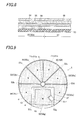
FIG. 5 is a plan view of thesolar panel 5 according to the present embodiment, andFIG. 6 is a cross-sectional view of thesolar panel 5 along a line VI-VI ofFIG. 5 . - As shown in
FIGS. 1 and5 , in an approximately central portion of thesolar panel 5, the through-hole 51 for inserting thehand spindle 31 is formed. - In the present embodiment, the
solar panel 5 includes not only the plurality of solar cells 50 (in the present embodiment, sixsolar cells 50a to 50f) which is light receiving sections, but also anon-power generation section 57 disposed at a position corresponding to theradiation electrode 42 of the circularlypolarized antenna 4. - Here, the position corresponding to the
radiation electrode 42 is a position above theradiation electrode 42. - As described above, since the circularly
polarized antenna 4 has the radiation pattern spreading from the peripheral portion of theradiation electrode 42, if the peripheral portion of theradiation electrode 42 is covered by a member inhibiting transmission of electric waves, the antenna characteristics (electric wave reception performance) deteriorates. - In order to prevent this, in the present embodiment, a portion of the
solar panel 5 which is to be positioned above theradiation electrode 42 consists of thenon-power generation section 57 which is made of only a non-conductive material, without containing conductive materials so as not to perform light reception and power generation. - Also, it is preferable that the size of the
non-power generation section 57 may be slightly larger than the size of theradiation electrode 42. In the present embodiment, thenon-power generation section 57 is formed such that each width of thenon-power generation section 57 is larger than each width of theradiation electrode 42 by 2 mm approximately all over the circumference. - As shown in
FIG. 6 , thesolar panel 5 has a structure in whichmetal electrodes 54, asemiconductor layer 55, andtransparent electrodes 56 are sequentially stacked on aresin substrate 53 to constitute the individualsolar cells 50. On thetransparent electrodes 56, a protective layer (protective film) 58 is stacked. Also, an insulatinglayer 59 is disposed on the side surfaces of the laminate structures composed of themetal electrodes 54, thesemiconductor layer 55, and thetransparent electrodes 56 to constitute the individualsolar cells 50. - The
resin substrate 53 is a flexible film-like substrate. The material which forms theresin substrate 53 is not especially limited. Theresin substrate 53 may be made of, for example, plastic. - The
metal electrodes 54 are made of a material containing a metal material such as an aluminum conductor. Also, the material which forms themetal electrodes 54 is not limited thereto. - The
semiconductor layer 55 is made of, for example, amorphous silicon (a-Si:H). As thesemiconductor layer 55, for example, a p-n junction type semiconductor having a junction between a p-type semiconductor and an n-type semiconductor can be used. - The
metal electrodes 54 and thesemiconductor layer 55 are stacked on theresin substrate 53 by a method such as deposition. Also, the method of forming themetal electrodes 54 and thesemiconductor layer 55 on theresin substrate 53 is not limited thereto. - Also, the
transparent electrodes 56 are formed by crystallizing, for example, zinc oxide, indium oxide, or tin oxide on a substrate such as glass. Also, the material and formation method of thetransparent electrodes 56 are not limited thereto. - Also, the
non-power generation section 57 of thesolar panel 5 is formed by removing themetal electrodes 54, thesemiconductor layer 55, and thetransparent electrodes 56 which are portions to be positioned above theradiation electrode 42. - The method of removing the
metal electrodes 54, thesemiconductor layer 55, and thetransparent electrodes 56 is not especially limited. For example, laser processing can be used. Also, instead of removing themetal electrodes 54, thesemiconductor layer 55, and thetransparent electrodes 56 stacked, themetal electrodes 54, thesemiconductor layer 55, and thetransparent electrodes 56 may be stacked while avoiding the portion where thenon-power generation section 57 will be provided (that is, the portion to be positioned above the radiation electrode 42). - In the present embodiment, the six
solar cells 50a to 50f are formed so as to have approximately equal areas as shown inFIGS. 1 and5 such that the output currents of the individual solar cells become substantially equal. - The
solar cells 50a to 50f are connected in series, and functions as one solar panel. - Specifically, the
solar cell 50a is electrically connected to the neighboringsolar cell 50b at aconnection portion 52a, and thesolar cell 50b is electrically connected to the neighboringsolar cell 50c at aconnection portion 52b. In the same way, thesolar cells 50c to 50e are electrically connected to the neighboringsolar cells 50d to 50f atconnection portions 52c to 52e. - Also, the
solar cell 50a is electrically connected to thepositive electrode 71p on thecircuit board 7, through theconnector 81 p. Thesolar cell 50f is electrically connected to thenegative electrode 71n on thecircuit board 7, through theconnector 81 n (seeFIG. 2 ). - As a result, the six
solar cells 50a to 50f are electrically connected to thecircuit board 7 in a state where they are connected in series. - Also, the connection positions where the
solar panel 5 and thecircuit board 7 are electrically connected, that is, the positions of the twoelectrodes circuit board 7 or the twoconnectors solar cells 50a to 50f are connected in series while being electrically connected to thecircuit board 7, and may be, for example, on thesolar cell 50c and thesolar cell 50d. - It is preferable that the connection positions may be positions apart from the circularly
polarized antenna 4 like in the present embodiment. Specifically, in a case of defining a boundary line as a line passing through the center of thesolar panel 5 while being perpendicular to a line connecting the center of the circularlypolarized antenna 4 and the center of thesolar panel 5, it is preferable that, as seen in a plan view of the solar panel, the connection positions may be provided in the opposite area (the upper half area ofFIG. 5 ) to an area (the lower half area ofFIG. 5 ) where the circularly polarizedantenna 4 is provided across the boundary line, in thesolar panel 5. In a case where the circularly polarizedantenna 4 is positioned as described above such that the center is in the area range from 4 o'clock to 7 o'clock through 6 o'clock on thedial plate 1 as seen in a plan view, it is more preferable that the corresponding connection positions may be in an area range from 8 o'clock to 12 o'clock through 2 o'clock on the dial plate 1 (seeFIG. 1 ). Also, the circularlypolarized antenna 4 is positioned while avoiding the center of thesolar panel 5 in this case. - Like this, since the connection positions of the
solar panel 5 and thecircuit board 7 are spaced apart from the circularlypolarized antenna 4, conductive materials (such as the twoelectrodes connectors polarized antenna 4. Therefore, the impedance of thesolar panel 5 around the position above the circularly polarizedantenna 4 becomes higher than the impedance of thesolar panel 5 in the vicinities of the connection positions apart from the circularlypolarized antenna 4. It is possible to reduce a bad influence (electromagnetic shield effect) of the conductive materials of the solar panel 5 (such as themetal electrodes 54, thesemiconductor layer 55, and thetransparent electrodes 56 of the solar cells 50) on GPS electric wave reception of the circularlypolarized antenna 4. - Also, in the present embodiment, a date wheel (not shown) is disposed in the
module 3, and adate display window 12 for displaying date is formed in thedial plate 1. - Further, in the
solar panel 5, at a position corresponding to thedate display window 12 of thedial plate 1, a date display opening 511 is formed. - In the present embodiment, the date display opening 511 is formed in the
non-power generation section 57 which is a part of thesolar panel 5 and does not perform light reception and power generation. - Therefore, it is possible to provide the date display opening 511 while suppressing influence on the power generation amount of the
solar panel 5, and rarely reducing the total area of the plurality ofsolar cells 50. - Next, the action of the
timepiece 100 according to the present embodiment will be described. - In the
timepiece 100 of the present embodiment, if light passing through thedial plate 1 from the viewable side enters thesolar panel 5 having thesolar cells 50a to 50f the light enters thesemiconductor layer 55 through thetransparent electrodes 56. If the light enters thesemiconductor layer 55, electrons and holes are generated around the junction between the p-type semiconductor and the n-type semiconductor. The generated electrons and holes move toward the n-type semiconductor and the p-type semiconductor, respectively, whereby an electromotive force (photoelectromotive force) is generated. As a result, current flows in circuits connected to thetransparent electrodes 56 and themetal electrodes 54. Electric power generated in this way by thesolar panel 5 is stored in thesecondary battery 6 through thecircuit board 7. - In this case, the
inductor 74 provided on the wiring route on thecircuit board 7 from thesolar panel 5 to thesecondary battery 6 has electric resistance of almost 0 Ω to the generated current (DC current) from thesolar panel 5, and thus does not block the generated current. As a result, electric power generated by thesolar panel 5 is appropriately stored in thesecondary battery 6. - Also, in the
timepiece 100, GPS electric waves passing through thedial plate 1 enter the circularly polarizedantenna 4. Then, theCPU 72 on thecircuit board 7 corrects the internal time of thetimepiece 100 to the exact time, based on time information and the like included in the GPS electric waves received by the circularly polarizedantenna 4. - In this case, due to the
inductor 74 provided on the wiring route on thecircuit board 7 from thesolar panel 5 to thesecondary battery 6, the impedance of a charging circuit connecting thesolar panel 5 and thesecondary battery 6 at the frequency of the GPS electric waves becomes extremely high. - Specifically, the impedance Z of the circuit is ideally expressed by Z = 2πfL. Here, f is the frequency of a signal, and L is the inductance value of the circuit. Since the frequency of the GPS electric waves is about 1.5 GHz as described above, and the inductance value of the
inductor 74 is about 1 mH as described above, from the above expression, the impedance Z of the corresponding charging circuit at the frequency of the GPS electric waves becomes about 10 kΩ. - Like this, since the impedance of the charging circuit at the frequency of the GPS electric waves increases, at the corresponding frequency, a current rarely flows in the charging circuit. Therefore, at the frequency of the GPS electric waves, since it is possible to make the electrical connection state of the
solar panel 5 and thecircuit board 7 an open state, it is possible to reduce a bad influence (electromagnetic shield effect) of the conductive materials of the solar panel 5 (such as themetal electrodes 54, thesemiconductor layer 55, and thetransparent electrodes 56 of the solar cells 50) on GPS electric wave reception of the circularlypolarized antenna 4. - Also, in this case, since the peripheral portion of the
radiation electrode 42 of the circularlypolarized antenna 4 is covered by the conductive materials (such as themetal electrodes 54, thesemiconductor layer 55, and thetransparent electrodes 56 of the solar cells 50), spreading of the radiation pattern is not inhibited, and the circularly polarizedantenna 4 can appropriately receive GPS electric waves. - As described above, according to the present embodiment, on the wiring route provided on the
circuit board 7 so as to electrically connect thesolar panel 5 and thesecondary battery 6, theinductor 74 is provided so as to have low DC resistance to a generated current from thesolar panel 5 while increasing impedance to electric waves which are received by the circularly polarizedantenna 4. - Therefore, it is possible to increase the impedance of the charging circuit at the frequency of GPS electric waves, without blocking a generated current from the
solar panel 5 to thesecondary battery 6, thereby reducing a bad influence of the conductive materials of thesolar panel 5 on GPS electric wave reception of the circularlypolarized antenna 4. Therefore, even in a case where thesolar panel 5 is disposed above the circularly polarizedantenna 4, it is possible to appropriately perform GPS electric wave reception of the circularlypolarized antenna 4 and charging of thesecondary battery 6, by simply providingonly inductor 74 on the wiring route connecting thesolar panel 5 and thesecondary battery 6. - Also, if two
inductors 74 are provided on two wiring routes on the positive electrode (71p) side and negative electrode (71n) side of thecircuit board 7, respectively, it is possible to further reduce a bad influence of the conductive materials of thesolar panel 5 on GPS electric wave reception of the circularlypolarized antenna 4. - Also, according to the present embodiment, the connection positions where the
solar panel 5 and thecircuit board 7 are electrically connected are positions apart from the circularlypolarized antenna 4. That is, in a case of defining a boundary line as a line passing through the center of thesolar panel 5 while being perpendicular to a line connecting the center of the circularlypolarized antenna 4 and the center of thesolar panel 5, as seen in a plan view, the connection positions are provided in the opposite area of the corresponding boundary line to the area where the circularly polarizedantenna 4 is provided, in thesolar panel 5. - Therefore, the conductive materials (such as the two
electrodes connectors polarized antenna 4, and the impedance of thesolar panel 5 around the position above the circularly polarizedantenna 4 becomes higher than the impedance of thesolar panel 5 in the vicinities of the connection positions apart from the circularlypolarized antenna 4. Therefore, it is possible to further reduce a bad influence of the conductive materials of thesolar panel 5 on GPS electric wave reception of the circularlypolarized antenna 4. - Also, according to the present embodiment, the circularly
polarized antenna 4 is disposed below thesolar panel 5, and thesolar panel 5 has thenon-power generation section 57 made of a non-conductive material at the position corresponding to theradiation electrode 42 of the circularlypolarized antenna 4. - Therefore, the peripheral portion of the
radiation electrode 42 is not covered by a conductive material. Therefore, it is possible to suppress deterioration of the antenna characteristics of the circularlypolarized antenna 4, and appropriately receive GPS electric waves. - Also, it goes not without saying that embodiments to which the present invention can be applied are not limited to the above described embodiment, and various modifications can be made without departing from the scope of the present invention.
- For example, in the above described embodiment, as a circuit element for increasing impedance to electric waves with the predetermined frequency which are received by the circularly polarized
antenna 4, theinductor 74 which is a choke coil having an inductance value of about 1 mH is provided. However, the circuit element is not limited thereto, and may be a choke coil having any other inductance value, or may be any other EMC countermeasure component such as a filter. - Also, in the above described embodiment, the
non-power generation section 57 which is provided at the position of thesolar panel 5 corresponding to theradiation electrode 42 consists of the non-conductive material remaining by removing the conductive materials (themetal electrodes 54 and the transparent electrodes 56) and the like. However, instead of providing thisnon-power generation section 57, an opening (a portion where theresin substrate 53 and theprotective layer 58 do not exist) is formed at the position corresponding to theradiation electrode 42. - Also, the
non-power generation section 57 of thesolar panel 5 may be formed by removing only themetal electrodes 54 as shown inFIGS. 7 and8 . - Here,
FIG. 7 is a plan view illustrating a modification of thesolar panel 5, andFIG. 8 is a cross-sectional view along a line VIII-VIII ofFIG. 7 . - As shown in
FIGS. 7 and8 , thenon-power generation section 57 may be provided by removing only themetal electrodes 54, such that it has thesemiconductor layer 55 and thetransparent electrodes 56 like thesolar cells 50. Although thetransparent electrodes 56 is configured by a conductive material, since the electrical conductivity of thetransparent electrodes 56 is lower than themetal electrodes 54 which is configured by an aluminum conductor or the like, a bad influence on the antenna characteristics of the circularlypolarized antenna 4 is relatively small. - Also, since the
non-power generation section 57 has thetransparent electrodes 56 and thesemiconductor layer 55 positioned on the front side, like thesolar cells 50, when thetimepiece 100 is viewed from the dial plate (1) side, thesolar cells 50 and thenon-power generation section 57 look the same. - Therefore, if the
non-power generation section 57 is configured by removing only themetal electrodes 54, it is possible to suppress deterioration of the antenna characteristics of the circularlypolarized antenna 4 while improving designability. - Also, the
non-power generation section 57 of thesolar panel 5 may be provided at a position corresponding to the peripheral portion of theradiation electrode 42 as shown inFIG. 9 . - Here,
FIG. 9 is a plan view illustrating another modification of thesolar panel 5. - As shown in
FIG. 9 , thenon-power generation section 57 may be provided in an annular shape only at a position corresponding to the peripheral portion of theradiation electrode 42 of the circularlypolarized antenna 4, not over theentire radiation electrode 42. As described above, in order to keep good antenna characteristics of the circularlypolarized antenna 4, it is important not to prevent spreading of the radiation pattern from the peripheral portion of theradiation electrode 42. For this reason, if thenon-power generation section 57 is provided only at a position corresponding to the peripheral portion of theradiation electrode 42, that is, a position above the corresponding peripheral portion, it is possible to sufficiently expect an effect to suppress deterioration of the antenna characteristics of the circularlypolarized antenna 4. In this case, thenon-power generation section 57 may be formed by removing only themetal electrodes 54 like in the above described modification. - Also, in this case, if an addition solar cell 50 (a
solar cell 50g) is provided on the inner side from the non-power generation section 57 (an area surrounded by the non-power generation section 57), it is possible to secure a wider light receiving section of thesolar panel 5, thereby improving power generation capacity. Also, in this case, it goes without saying that the addedsolar cell 50g is electrically connected in series to the othersolar cells 50a to 50f (for example, byconnection portions FIG. 9 ) and is formed so as to have an area substantially equal to those of the othersolar cells 50a to 50f. - Therefore, if the
non-power generation section 57 is provided at a position corresponding to the peripheral portion of theradiation electrode 42, it is possible to suppress deterioration of the antenna characteristics of the circularlypolarized antenna 4 while improving the power generation capacity of thesolar panel 5. - Also, the division method of the solar panel (such as the number of partitions and the shape of each divided solar cell) is not limited to that exemplified in the above described embodiment.
- Also, in the above described embodiment, a case of providing one circularly
polarized antenna 4 has been exemplified. However, the number of circularlypolarized antennae 4 to be provided in the timepiece is not limited thereto. - Also, the antenna according to the present invention is not limited to a circularly polarized antenna for receiving GPS electric waves, and needs only to be an antenna able to receive electric waves with a predetermined frequency, such as an antenna corresponding to Bluetooth (a registered trademark) or any other high-frequency wireless communication.
- Also, in the above described embodiment, a case where the timepiece which is the electronic device is the
analog type timepiece 100 which rotates the clock hands 2 on thedial plate 1, thereby displaying time and the like has been exemplified. However, the timepiece is not limited to the analog type timepiece. - The timepiece may be, for example, a digital type timepiece having a dial plate (such as a liquid crystal display unit) for displaying various information such as time and calendar information by characters and the like. Also, a dial plate having both of an analog type display unit and a digital type display unit may be included in the electronic device.
- Also, in the above described embodiment, a case where the electronic device according to the present invention is a timepiece (electronic timepiece) has been exemplified. However, the corresponding electronic device is not limited thereto.
- The electronic device according to the present invention needs only to perform photovoltaic power generation by a solar panel, store the generated electric power in a secondary battery, and receive electric waves with a predetermined frequency by an antenna disposed near the solar panel, and may be, for example, a biological information display such as a pedometer, a heart rate meter, or a pulsimeter, or a display for displaying various information such as movement distance and movement pace information, altitude information, and air pressure information.
- Though several embodiments of the present invention have been described above, the scope of the present invention is not limited to the above embodiments, and includes the scope of inventions, which is described in the scope of claims, and the scope equivalent thereof.
Claims (4)
- An electronic device comprising:a solar panel (5) that receives light to generate electric power;a secondary battery (6) that stores electric power generated by the solar panel;an antenna (4) that is disposed near the solar panel and that receives electric waves with a predetermined frequency; anda circuit board (7) that electrically connects the solar panel and the secondary battery,wherein, on a wiring route which is formed on the circuit board so as to electrically connect the solar panel and the secondary battery, at least one circuit element (74) is provided so as to have high electric resistance with respect to electric waves which are received by the antenna while having low electric resistance with respect to a generated current from the solar panel.
- The electronic device according to claim 1, wherein:the circuit board includes a positive electrode and a negative electrode to which the solar panel is electrically connected respectively, andcircuit elements are provided on a wiring route of a positive electrode side and on a wiring route of a negative electrode side, respectively.
- The electronic device according to claim 1 or 2, wherein:the solar panel and the circuit board are electrically connected at connection positions,a boundary line passes through a center of the solar panel and is perpendicular to a line connecting a center of the antenna and the center of the solar panel, andthe connection positions are provided in an opposite area to an area where the antenna is provided across the boundary line, in a plan view of the solar panel.
- The electronic device according to any one of claims 1 through 3, wherein:the electronic device is an electronic timepiece (100) for displaying time.
Applications Claiming Priority (1)
| Application Number | Priority Date | Filing Date | Title |
|---|---|---|---|
| JP2014133744A JP6119683B2 (en) | 2014-06-30 | 2014-06-30 | Electronics |
Publications (2)
| Publication Number | Publication Date |
|---|---|
| EP2963508A2 true EP2963508A2 (en) | 2016-01-06 |
| EP2963508A3 EP2963508A3 (en) | 2016-03-16 |
Family
ID=53373332
Family Applications (1)
| Application Number | Title | Priority Date | Filing Date |
|---|---|---|---|
| EP15171294.0A Ceased EP2963508A3 (en) | 2014-06-30 | 2015-06-10 | Electronic device |
Country Status (4)
| Country | Link |
|---|---|
| US (1) | US20150378313A1 (en) |
| EP (1) | EP2963508A3 (en) |
| JP (1) | JP6119683B2 (en) |
| CN (1) | CN105319947B (en) |
Families Citing this family (12)
| Publication number | Priority date | Publication date | Assignee | Title |
|---|---|---|---|---|
| US20170023612A1 (en) * | 2015-07-22 | 2017-01-26 | Iometers, LLC | Meter Box Lid |
| CN105974783B (en) * | 2016-06-16 | 2019-03-05 | 浙江卓越电子有限公司 | A kind of smartwatch cassette mechanism structure |
| CN105974784B (en) * | 2016-06-16 | 2019-03-05 | 浙江卓越电子有限公司 | A kind of timepiece movement structure of anti-vibration |
| EP3482474A4 (en) | 2016-06-20 | 2020-07-29 | Ami Research&development, LLC | Low frequency rectenna system for wireless charging |
| US10732578B2 (en) * | 2016-11-08 | 2020-08-04 | Seiko Epson Corporation | Electronic timepiece |
| JP6874453B2 (en) * | 2017-03-21 | 2021-05-19 | セイコーエプソン株式会社 | Electronic clock |
| JP2019032221A (en) | 2017-08-08 | 2019-02-28 | セイコーエプソン株式会社 | Portable electronic apparatus |
| JP7098946B2 (en) * | 2018-02-01 | 2022-07-12 | セイコーエプソン株式会社 | Movements and watches with solar cells |
| JP7073833B2 (en) * | 2018-03-23 | 2022-05-24 | セイコーエプソン株式会社 | Electronic clock |
| JP7151453B2 (en) * | 2018-12-18 | 2022-10-12 | セイコーエプソン株式会社 | electronic clock |
| JP7078024B2 (en) * | 2019-10-15 | 2022-05-31 | カシオ計算機株式会社 | Solar panels, electronic devices and electronic clocks |
| JP7310553B2 (en) * | 2019-11-06 | 2023-07-19 | セイコーエプソン株式会社 | electronic clock |
Citations (1)
| Publication number | Priority date | Publication date | Assignee | Title |
|---|---|---|---|---|
| JP2010066151A (en) | 2008-09-11 | 2010-03-25 | Seiko Epson Corp | Wrist device |
Family Cites Families (17)
| Publication number | Priority date | Publication date | Assignee | Title |
|---|---|---|---|---|
| US5027051A (en) * | 1990-02-20 | 1991-06-25 | Donald Lafferty | Photovoltaic source switching regulator with maximum power transfer efficiency without voltage change |
| WO2000028513A1 (en) * | 1998-11-10 | 2000-05-18 | Citizen Watch Co., Ltd. | Electronic device with solar cell |
| EP1126337A4 (en) * | 1998-11-26 | 2002-04-17 | Citizen Watch Co Ltd | Timepiece |
| KR100722083B1 (en) * | 2003-05-09 | 2007-05-25 | 세이코 엡슨 가부시키가이샤 | Electronic watch with wireless communication function |
| JP2007187504A (en) * | 2006-01-12 | 2007-07-26 | Seiko Instruments Inc | Digital display type radio-controlled clock, and method of receiving standard wave of the clock |
| JP5599472B2 (en) * | 2009-12-30 | 2014-10-01 | タイコ エレクトロニクス サービス ゲーエムベーハー | Antenna device with frequency dependent connection to electrical ground |
| JP5307105B2 (en) * | 2010-01-06 | 2013-10-02 | 株式会社神戸製鋼所 | COMPOSITE WINDING ELEMENT AND COMPOSITE WINDING ELEMENT FOR TRANSFORMER, TRANSFORMATION SYSTEM AND NOISE CUT FILTER USING SAME |
| JP2011208948A (en) * | 2010-03-26 | 2011-10-20 | Citizen Holdings Co Ltd | Radio controlled watch |
| JP5531830B2 (en) * | 2010-07-05 | 2014-06-25 | セイコーエプソン株式会社 | Electronic clock |
| KR101678222B1 (en) * | 2010-09-30 | 2016-11-21 | 삼성전자주식회사 | A portable terminal having keypad |
| JP5598257B2 (en) * | 2010-10-28 | 2014-10-01 | カシオ計算機株式会社 | Electronics |
| JP5866860B2 (en) * | 2011-01-05 | 2016-02-24 | セイコーエプソン株式会社 | Clock with wireless function |
| JP5742349B2 (en) * | 2011-03-23 | 2015-07-01 | セイコーエプソン株式会社 | ANTENNA DEVICE AND ELECTRONIC DEVICE |
| CN202587606U (en) * | 2012-05-30 | 2012-12-05 | 江苏伟信电子有限公司 | FPC (Flexible Printed Circuit) for mobile phone antenna |
| JP5962252B2 (en) * | 2012-06-25 | 2016-08-03 | セイコーエプソン株式会社 | Electronic clock with solar battery |
| CN103078172B (en) * | 2013-02-20 | 2015-03-25 | 上海安费诺永亿通讯电子有限公司 | Antenna with high-sensitivity induction device |
| US10039492B2 (en) * | 2014-06-13 | 2018-08-07 | Verily Life Sciences, LLC | Conditional storage |
-
2014
- 2014-06-30 JP JP2014133744A patent/JP6119683B2/en active Active
-
2015
- 2015-06-03 US US14/729,414 patent/US20150378313A1/en not_active Abandoned
- 2015-06-10 EP EP15171294.0A patent/EP2963508A3/en not_active Ceased
- 2015-06-19 CN CN201510347401.9A patent/CN105319947B/en active Active
Patent Citations (1)
| Publication number | Priority date | Publication date | Assignee | Title |
|---|---|---|---|---|
| JP2010066151A (en) | 2008-09-11 | 2010-03-25 | Seiko Epson Corp | Wrist device |
Also Published As
| Publication number | Publication date |
|---|---|
| JP6119683B2 (en) | 2017-04-26 |
| EP2963508A3 (en) | 2016-03-16 |
| CN105319947B (en) | 2019-04-30 |
| US20150378313A1 (en) | 2015-12-31 |
| CN105319947A (en) | 2016-02-10 |
| JP2016011897A (en) | 2016-01-21 |
Similar Documents
| Publication | Publication Date | Title |
|---|---|---|
| EP2963508A2 (en) | Electronic device | |
| JP6428823B2 (en) | Electronics | |
| US9891597B2 (en) | Electronic device | |
| CN102467085B (en) | Electronic device equipped with antenna device and solar panel | |
| CN104950664B (en) | Possesses the electronic equipment of solar panel | |
| JP6696195B2 (en) | Electronic clock | |
| JP6488548B2 (en) | Electronics | |
| US8482470B2 (en) | Electric device with an antenna device and a solar panel | |
| US11537083B2 (en) | Electronic timepiece | |
| JP7107089B2 (en) | electronic clock | |
| JP2019191146A (en) | Electronic timepiece | |
| JP6264987B2 (en) | Electronics | |
| JP6575588B2 (en) | Solar panels and electronics | |
| CN112671327A (en) | Solar panel, electronic device, and electronic timepiece | |
| CN112213935B (en) | Clock and watch | |
| JP6423744B2 (en) | Satellite radio clock |
Legal Events
| Date | Code | Title | Description |
|---|---|---|---|
| PUAI | Public reference made under article 153(3) epc to a published international application that has entered the european phase |
Free format text: ORIGINAL CODE: 0009012 |
|
| 17P | Request for examination filed |
Effective date: 20150610 |
|
| AK | Designated contracting states |
Kind code of ref document: A2 Designated state(s): AL AT BE BG CH CY CZ DE DK EE ES FI FR GB GR HR HU IE IS IT LI LT LU LV MC MK MT NL NO PL PT RO RS SE SI SK SM TR |
|
| AX | Request for extension of the european patent |
Extension state: BA ME |
|
| PUAL | Search report despatched |
Free format text: ORIGINAL CODE: 0009013 |
|
| AK | Designated contracting states |
Kind code of ref document: A3 Designated state(s): AL AT BE BG CH CY CZ DE DK EE ES FI FR GB GR HR HU IE IS IT LI LT LU LV MC MK MT NL NO PL PT RO RS SE SI SK SM TR |
|
| AX | Request for extension of the european patent |
Extension state: BA ME |
|
| RIC1 | Information provided on ipc code assigned before grant |
Ipc: G04C 10/02 20060101ALI20160208BHEP Ipc: G04R 60/10 20130101AFI20160208BHEP |
|
| STAA | Information on the status of an ep patent application or granted ep patent |
Free format text: STATUS: THE APPLICATION HAS BEEN REFUSED |
|
| 18R | Application refused |
Effective date: 20200206 |