EP2952915A1 - Messung von strom mit breitem spektrum mittels variablem widerstand - Google Patents
Messung von strom mit breitem spektrum mittels variablem widerstand Download PDFInfo
- Publication number
- EP2952915A1 EP2952915A1 EP15168885.0A EP15168885A EP2952915A1 EP 2952915 A1 EP2952915 A1 EP 2952915A1 EP 15168885 A EP15168885 A EP 15168885A EP 2952915 A1 EP2952915 A1 EP 2952915A1
- Authority
- EP
- European Patent Office
- Prior art keywords
- current
- sense
- interface
- sensor
- transistor
- Prior art date
- Legal status (The legal status is an assumption and is not a legal conclusion. Google has not performed a legal analysis and makes no representation as to the accuracy of the status listed.)
- Granted
Links
- 238000005259 measurement Methods 0.000 title abstract description 23
- 238000000034 method Methods 0.000 claims abstract description 29
- 230000004044 response Effects 0.000 claims abstract description 17
- 238000012545 processing Methods 0.000 claims description 2
- 230000008901 benefit Effects 0.000 description 10
- 238000010586 diagram Methods 0.000 description 9
- 239000004065 semiconductor Substances 0.000 description 3
- 230000003247 decreasing effect Effects 0.000 description 2
- 238000013461 design Methods 0.000 description 2
- 230000006870 function Effects 0.000 description 2
- 230000003213 activating effect Effects 0.000 description 1
- 238000004891 communication Methods 0.000 description 1
- 230000008878 coupling Effects 0.000 description 1
- 238000010168 coupling process Methods 0.000 description 1
- 238000005859 coupling reaction Methods 0.000 description 1
- 238000005516 engineering process Methods 0.000 description 1
- 230000005669 field effect Effects 0.000 description 1
- 230000007246 mechanism Effects 0.000 description 1
- 230000002093 peripheral effect Effects 0.000 description 1
- 238000005381 potential energy Methods 0.000 description 1
- 230000036632 reaction speed Effects 0.000 description 1
Images


Classifications
-
- G—PHYSICS
- G01—MEASURING; TESTING
- G01R—MEASURING ELECTRIC VARIABLES; MEASURING MAGNETIC VARIABLES
- G01R19/00—Arrangements for measuring currents or voltages or for indicating presence or sign thereof
- G01R19/0092—Arrangements for measuring currents or voltages or for indicating presence or sign thereof measuring current only
-
- G—PHYSICS
- G01—MEASURING; TESTING
- G01R—MEASURING ELECTRIC VARIABLES; MEASURING MAGNETIC VARIABLES
- G01R19/00—Arrangements for measuring currents or voltages or for indicating presence or sign thereof
- G01R19/0023—Measuring currents or voltages from sources with high internal resistance by means of measuring circuits with high input impedance, e.g. OP-amplifiers
-
- H—ELECTRICITY
- H03—ELECTRONIC CIRCUITRY
- H03K—PULSE TECHNIQUE
- H03K17/00—Electronic switching or gating, i.e. not by contact-making and –breaking
- H03K17/08—Modifications for protecting switching circuit against overcurrent or overvoltage
- H03K17/082—Modifications for protecting switching circuit against overcurrent or overvoltage by feedback from the output to the control circuit
- H03K17/0822—Modifications for protecting switching circuit against overcurrent or overvoltage by feedback from the output to the control circuit in field-effect transistor switches
-
- G—PHYSICS
- G01—MEASURING; TESTING
- G01R—MEASURING ELECTRIC VARIABLES; MEASURING MAGNETIC VARIABLES
- G01R1/00—Details of instruments or arrangements of the types included in groups G01R5/00 - G01R13/00 and G01R31/00
- G01R1/20—Modifications of basic electric elements for use in electric measuring instruments; Structural combinations of such elements with such instruments
- G01R1/203—Resistors used for electric measuring, e.g. decade resistors standards, resistors for comparators, series resistors, shunts
-
- G—PHYSICS
- G01—MEASURING; TESTING
- G01R—MEASURING ELECTRIC VARIABLES; MEASURING MAGNETIC VARIABLES
- G01R19/00—Arrangements for measuring currents or voltages or for indicating presence or sign thereof
- G01R19/165—Indicating that current or voltage is either above or below a predetermined value or within or outside a predetermined range of values
- G01R19/16504—Indicating that current or voltage is either above or below a predetermined value or within or outside a predetermined range of values characterised by the components employed
- G01R19/16519—Indicating that current or voltage is either above or below a predetermined value or within or outside a predetermined range of values characterised by the components employed using FET's
-
- G—PHYSICS
- G01—MEASURING; TESTING
- G01R—MEASURING ELECTRIC VARIABLES; MEASURING MAGNETIC VARIABLES
- G01R31/00—Arrangements for testing electric properties; Arrangements for locating electric faults; Arrangements for electrical testing characterised by what is being tested not provided for elsewhere
- G01R31/005—Testing of electric installations on transport means
-
- H—ELECTRICITY
- H03—ELECTRONIC CIRCUITRY
- H03K—PULSE TECHNIQUE
- H03K2217/00—Indexing scheme related to electronic switching or gating, i.e. not by contact-making or -breaking covered by H03K17/00
- H03K2217/0027—Measuring means of, e.g. currents through or voltages across the switch
Definitions
- MOSFET Metal-Oxide-Semiconductor Field Effect Transistor
- sensing techniques involve providing a sense MOSFET coupled to the main MOSFET device to draw a small sensor current that is proportional to the main current.
- the sense MOSFET is smaller than the main MOSFET device by a particular ratio, which defines the proportion of current drawn by the sense MOSFET.
- the ratio is typically low.
- the ratio should be high in order to achieve high efficiency. High efficiency typically means that the sense MOSFET causes very low power losses.
- Embodiments of an apparatus for sensing current through a transistor device may include an interface configured to receive a current from the transistor device for sensing.
- the apparatus may also include a sensor component coupled to the interface and configured to receive the current from the transistor device and to generate a responsive sensor voltage, the sensor component comprising an adjustable resistance component, a resistance value of the adjustable resistance component being selectable in response to a level of the current received at the interface.
- the apparatus may further comprise a sense control circuit configured to control a duty cycle of the sensor component.
- the sense control circuit may further comprise an automatic ranging device configured to automatically scale the resistance in response to a magnitude value of the current.
- the automatic ranging device may be configured to switch the current to a resistor in the sense component on and off according to the duty cycle of the sensor component.
- the sense control circuit may further comprise a comparator configured to trigger adjustment of the adjustable resistance component in response to an output voltage of the sensor component crossing a threshold set by a reference voltage.
- Embodiments of an integrated circuit for sensing current through a transistor device may include an interface configured to receive a current from the transistor device for sensing. Additionally, embodiments may include a sensor component coupled to the interface and configured to receive the current from the transistor device and to generate a responsive sensor voltage, the sensor component comprising an adjustable resistance component, a resistance value of the adjustable resistance component being selectable in response to a level of the current received at the interface.
- the integrated circuit may further comprise a sense control circuit configured to control a duty cycle of the sensor component.
- the sense control circuit may further comprise an automatic ranging device configured to automatically scale the resistance in response to a magnitude value of the current.
- the automatic ranging device may be configured to switch the current to a resistor in the sense component on and off according to the duty cycle of the sensor component.
- the sense control circuit may further comprise a comparator configured to trigger adjustment of the adjustable resistance component in response to an output voltage of the sensor component crossing a threshold set by a reference voltage.
- the interface may comprise: a gate node interface configured interface with a gate node of the transistor device; a drain node interface configured to interface with a drain node of the transistor device; a source node interface configured to interface with a source node; a Kelvin node interface configured to interface with a Kelvin node of the transistor device; and a sense current node interface configured to receive the current from the a sense current node of the transistor device, the current being a sense current that is smaller than a main current that flows through the transistor device by a predetermined ratio.
- the integrated circuit may further comprising an Operational Amplifier (OPAMP) coupled to the sense node interface and the Kelvin node interface and configured to force a voltage value at the sense node interface and at the Kelvin node interface to equal levels.
- OPAMP Operational Amplifier
- the integrated circuit may further comprise a current sense transistor coupled to the OPAMP, the current sense transistor configured to drive a current to the sensor component for generating a sensor voltage across the current sense component.
- the integrated circuit may further comprise: a plurality of interfaces an interface each configured to receive a current from one of a plurality of transistor devices for sensing; a plurality of sensor components, each coupled to one of the plurality of interfaces; and a shared Analog to Digital (ADC) converter coupled to each of the plurality of sensor components, the ADC configured to convert analog sensor data into digital sensor data.
- a plurality of interfaces an interface each configured to receive a current from one of a plurality of transistor devices for sensing
- a plurality of sensor components each coupled to one of the plurality of interfaces
- a shared Analog to Digital (ADC) converter coupled to each of the plurality of sensor components, the ADC configured to convert analog sensor data into digital sensor data.
- ADC Analog to Digital
- the integrated circuit may further comprise a digital format converter configured to reformat the digital sensor data into a digital data format that is readable by an external data processing device.
- embodiments of a method for sensing current through a transistor device may include receiving a current from the transistor device for sensing at an interface configured to receive the current from the transistor device.
- the methods may also include generating a sensor voltage with a sensor component, the sensor component comprising an adjustable resistance component. Also, the methods may include selecting a resistance value of the adjustable resistance component in response to a level of the current received at the interface.
- the method may further comprise controlling a duty cycle of the sensor component using a sense control circuit.
- the method may further comprise automatically scaling the resistance in response to a magnitude value of the current, wherein the sense control circuit further comprises an automatic ranging device configured to control the automatic scaling.
- the method may further comprise switching the current to a resistor in the sense component on and off according to the duty cycle of the sensor component using the automatic ranging device.
- the method may further comprise triggering adjustment of the adjustable resistance component in response to an output voltage of the sensor component crossing a threshold set by a reference voltage.
- Embodiments of devices for broad-range current measurement using variable resistance may be implemented in a number of different types of electronic devices.
- Some examples of electronic devices include semiconductor devices for automotive or marine applications, controllers for factory automation systems, components of alternative power systems, etc. There is no limitation on the general types of applications that might incorporate embodiments of the technology described herein.
- Advantages of the present embodiments include an ability to provide current sensing in a single sensor circuit that exhibits both high accuracy and high efficiency. Another advantage is that the present embodiments do not require a large circuit footprint, since an Analog to Digital Converter (ADC) may be shared amongst multiple channels. Additionally, the circuit footprint required for digital level shifters between high side domains and low-side domain may be reduced because the level shifters may be functionally replaced by components of the sensor circuitry.
- ADC Analog to Digital Converter
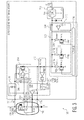
- Fig. 1 depicts a schematic circuit diagram of one embodiment of a transistor circuit 100.
- the transistor circuit 100 includes a main transistor 102 and a sense transistor 104.
- the main transistor 102 may be, for example, a MOSFET device.
- the MOSFET device may be a power MOSFET configured to conduct high currents for automotive applications, for example.
- the sense transistor 104 may also be a MOSFET device.
- the main transistor 102 and the sense transistor 104 are each connected to a drain node (D) 106 and a gate node (G) 108.
- the main transistor 102 includes a Kelvin node (K) 112 for providing an accurate measurement of the potential at a source node 110 of the main transistor 102.
- the sense transistor 104 may provide a sense current to a sense current node (I SENSE ) 114.
- the embodiment of Fig. 1 provides a main transistor 102 configured to conduct a current (I SOURCE ) and a sense transistor 104 configured to provide a measurable sense current (I SENSE ), which may be a portion of the current (I SOURCE ), for external sensing.
- the sense transistor 104 may be configured to provide a sense current that is smaller than the main current by a predetermined ratio. For example, the ratio may be determined by the relative size of the main transistor 102 and the sense transistor 104. If, for example, the main transistor 102 is n times larger than the sense transistor 104, the sense transistor 104 may be configured to provide a sense current that is 1 / n th of the main current.
- Fig. 2 depicts a schematic block diagram of a system 200 for sensing a current in the transistor circuit 100.
- the system 200 is implemented in an integrated circuit.
- the transistor circuit 100 is a MOSFET configured to conduct a main current (I SOURCE ) as illustrated in Fig. 1 .
- the transistor circuit 100 may include both the main transistor 102 and the sense transistor 104 as described in Fig. 1 .
- the main transistor 102 and the sense transistor 104 may be integrated into a transistor device package as illustrated by the transistor circuit 100 in Fig. 2 .
- the system 200 includes a current sense device 202.
- the current sense device 202 may be coupled to the transistor circuit 100.
- the current sense device may include a battery interface 220 for coupling to the drain node 106 of the transistor device.
- the current sense device 202 may include a gate interface 222, a source interface 226, a Kelvin interface 224, and a sense current interface 228, each configured to be respectively coupled to the gate node 108, the source node 110, the Kelvin node 112, and the sense current node 114 of the transistor circuit 100.
- the current sense device 202 may be a stand-alone integrated circuit device having I/O pins corresponding to the gate interface 222, the source interface 226, the Kelvin interface 224, and the sense current interface 228.
- the sense device includes an OPAMP 204 configured to force the voltage on the Kelvin interface 224 and the sense current interface 228 to be equal, such that the main transistor 102 and the sense transistor 104 operate on the same gate-source voltage difference. Because Gate-source voltages of the main transistor 102 and the sense transistor 104 are equal, a current n times smaller than the current that flows through the main transistor 102 will flow through the sense transistor 104, when the sense transistor 104 is n times smaller than the main device 102, and is sensed in the current sense device 202. In an embodiment, the sense current will flow through transistor (M1) 218 and generate a large voltage across the sense resistor 216 that can be further processed.
- the illustrated current sense device 202 is shown with certain components and described with certain functionality herein, other embodiments of semiconductor chips and corresponding systems may include fewer or more components to implement the same, less, or more functionality.
- the gate driver 214 drives the gate node 108 of the transistor circuit 100.
- the Charge Pump (CP) 208 may be configured to provide a voltage supply for the transistor circuit 100, which may include one or more NMOSFET devices configured to operate in a high-side configuration. In a high-side configuration, the gate voltage may be larger than the supply voltage (battery voltage, VBAT), which is generated by the charge pump 208.
- the Overcurrent Comparator (OC Comp) 212 detects a current larger than the nominal current range. In an embodiment, the overcurrent may be detected by a voltage comparator between the battery terminal 220 and the source terminal 226.
- a current sensing block 210 may include an Analog to Digital Converter (ADC) configured to convert a current sense voltage at the sense resistor 216 into digital sensor data that can be used by external digital components, such as digital controllers.
- ADC Analog to Digital Converter
- the voltage across the source resistance (Rsource) 230 may be low (I * Rsource) as compared with the embodiments of Figs. 3-4 .
- the voltage across Rsource 230 can be as low as 5 ⁇ V up to about 20mV in some embodiments.
- the voltage across Rsource 230 is not only at the non-inverting input of the OPAMP 204, but also at the inverting input of OPAMP 204, which also represents the full headroom available for M1 218 and the sense resistor Rsense 216. Therefore, the voltage across the sense resistor 216 is effectively lower than the levels at Rsource 230.
- the voltage at the sense resistor 216 may only be half of the voltage at Rsource 230. Therefore, it may be challenging to design circuitry for sensing voltages between 5 ⁇ V and 10 mV with high accuracy and high resolution.
- Fig. 3 illustrates another embodiment of a system 300 for broad-range current measurement using variable resistance.
- the OPAMP 204 forces the voltage levels at the K interface 224 and the sense current interface 228 to be equal.
- the sense current may be n times smaller than the main current (I), and may flow to ground via sense resistors 216a-n (Rsense1,...n) in sensor component 302.
- the voltage level across the sense resistor(s) 216a-n in sensor component 302 may be significantly higher than in the circuit 200 of Fig. 2 .
- the sensor device 202 may be less sensitive to EMC exposure.
- a sense control circuit 310 may configure the sensor component 302 such that the resistance of the sensor component 302 is adjusted in value depending on the absolute value of the current (I) and the sense current (I/n).
- the sense control circuit 310 may include a reference comparator 304 and an auto-range circuit 306. Such an embodiment, with adjustable resistance, will allow the measurement over a wide current range with high accuracy and resolution.
- the reference comparator 304 may be configured to compare the output voltage of the sensor component 302 to a reference voltage and provide feedback to the auto-range circuit 306.
- the voltage may be 1.8 V.
- the auto-range circuit 306 may then cause another sense resistor 216a-n in the sensor component 302 to be activated.
- the auto-range circuit 306 may apply a voltage to a switch transistor 308a-n (Mrange1,...n) causing current to flow through the corresponding sense resistor 216a-n.
- a sense current may be received at the sense current interface 228 and conducted through transistor 218 (M1) to sensor component 302.
- a first switch transistor 308a (Mrange1) may be activated causing the current to flow through the corresponding first sense resistor 216a.
- the reference comparator 304 may compare the voltage across the first sense resistor 216a with the reference voltage and determine that the voltage on the first sense resistor 216a is too high.
- a feedback signal may be sent to sense control circuit 310, which causes auto-range circuit 306 to deactivate the first switch transistor 308a and activate the second switch transistor 308b.
- Activating the second switch transistor 308b may then cause the current to flow through the second sense resistor 216b, which may have a different resistance value than the first sense resistor 216a.
- the resistance value of the sensor component 302 may be automatically adjusted or scaled according to the value of the current received at the sense current interface 228.
- the switch transistors 308a-n may be activated in parallel, rather than in sequence.
- the power dissipation may be high where the value of n in the ratio I / n is low for enhanced accuracy.
- the sense component 302 may be activated and deactivated periodically.
- the graph of Fig. 4 illustrates the sensor output voltage 402 verses time 404.
- the sensor component 302 may generate a sensor output signal 406 which is activated for a portion 408 ( t on ) of the period 410 (T) and deactivated for the remainder of the period 410.
- the auto-range circuit 306 may control the duty cycle of the sensor component 302 by periodically switching the switch transistors 308a-n on and off according to a preconfigured duty cycle period.
- the auto-range circuit 306 may be pre-configured to control the duty cycle of the sensor component 302 according to a predetermined duty cycle function.
- the duty cycle based measurement may not detrimentally affect accuracy, because the size ratio n may not be decreased by decreasing the size of the sense MOSFET. Rather, the ratio n may be effectively increased by the duty cycle based measurement. In such an embodiment, both accuracy and resolution parameters may be improved as compared to other systems.
- duty cycle based sensing will decrease the reaction speed of the current sense device 202 on changes in the main current (I SOURCE ). Nonetheless, duty cycle ratios as low as 40% may be suitable for use with the present embodiments.
- Fig. 5 depicts a system 500 having a four channel high accuracy, high efficiency current measurement device 502.
- the four channel current measurement device 502 may sense the current I1...I4 through four individual channels with high accuracy and high efficiency.
- each channel is coupled to a separate transistor circuit 100.
- a first transistor circuit 100a may be coupled to a first current sensing device 202a
- a second transistor circuit 100b may be coupled to a second current sensing device 202b
- a third transistor circuit 100c may be coupled to a third current sensing device 202c
- a fourth transistor circuit 100d may be coupled to a fourth current sensing device 202d.
- each channel may include a current sensing device 202a-d, each being coupled to a shared ADC 504, which is a more area effective solution compared with a single ADC 210 per channel.
- the digital output of the shared ADC 504 may be communicated to a main digital block 508.
- the main digital block 508 may use frequency information generated by the oscillator 506 to reformat the digital sensor signals for communication to an external microprocessor over, for example, a Serial Peripheral Interface (SPI) bus interface 510, which may include multiple discrete lines in one embodiment.
- SPI Serial Peripheral Interface
- the current measurement device 502 may be a stand-alone integrated circuit device.
- Fig. 6 depicts a flowchart diagram of one embodiment of a method 600 for broad-range current measurement using variable resistance.
- the method 600 starts at block 602 with receiving a current from the transistor device for sensing at an interface configured to receive the current from the transistor device.
- the method includes generating a sensor voltage with a sensor component, the sensor voltage being responsive to the current from the transistor device.
- the method includes controlling a duty cycle of the sensor component with a sense control circuit.
- gate driver 214 may drive a voltage at the gate node 108 causing current I SOURCE to flow from the battery interface 220 through the main transistor 102 to the source node 110, as shown at block 602.
- the sense transistor 104 may simultaneously conduct the sense current I s to the sense current node 114.
- the sense current I SENSE may then flow through sense current interface 228 to the inverting terminal of OPAMP 204 and through sensor transistor 218.
- the sense current only flows through sensor transistor 218 when the potential energy at the K terminal 224 and the sense current interface 228 is equal.
- the current flows through sensor transistor 218 to sensor component 302, where a voltage is established over the one or more sensor resistors 216a-n (Rsense1,...n).
- the voltage is then converted by ADC 210 and provided as digital sensor data to an external component.
- the sensing may be duty cycled as described with reference to Fig. 4 .
- the voltage may only be sensed during the t on portion 408 of the sensing period 410 as controlled by the duty cycle settings of the sense control circuit 310.
- multiple currents may flow through multiple transistor circuits 100a-d and sensed by a multi-channel current sensor device 502 as described with reference to Fig. 5 .
- Fig. 7 illustrates another embodiment of a method 700 for broad-range current measurement using variable resistance.
- the method 700 starts at block 702, by receiving a current from the transistor device for sensing at an interface configured to receive the current from the sensor device.
- the method includes generating a responsive sensor voltage with a sensor component, the sensor component comprising an adjustable resistance component.
- the method 700 further includes selecting a value of the adjustable resistance component in response to a level of the current received at the interface, as shown at block 706.
- firmware or software instructions stored on a readable storage medium for execution by a programmable logic device, such as an Application Specific Integrated Circuit (ASIC), a Field Programmable Gate Array (FPGA), a Programmable Logic Chip (PLC), a processor, or the like.
- ASIC Application Specific Integrated Circuit
- FPGA Field Programmable Gate Array
- PLC Programmable Logic Chip
- an embodiment of a program product includes a firmware package stored on a flash memory device and configured to cause an FPGA to perform the operations described herein.
Landscapes
- Physics & Mathematics (AREA)
- General Physics & Mathematics (AREA)
- Measurement Of Current Or Voltage (AREA)
Applications Claiming Priority (1)
| Application Number | Priority Date | Filing Date | Title |
|---|---|---|---|
| US14/289,420 US9720020B2 (en) | 2014-05-28 | 2014-05-28 | Broad-range current measurement using variable resistance |
Publications (2)
| Publication Number | Publication Date |
|---|---|
| EP2952915A1 true EP2952915A1 (de) | 2015-12-09 |
| EP2952915B1 EP2952915B1 (de) | 2020-01-15 |
Family
ID=53191550
Family Applications (1)
| Application Number | Title | Priority Date | Filing Date |
|---|---|---|---|
| EP15168885.0A Active EP2952915B1 (de) | 2014-05-28 | 2015-05-22 | Messung von strom mit breitem spektrum mittels variablem widerstand |
Country Status (4)
| Country | Link |
|---|---|
| US (1) | US9720020B2 (de) |
| EP (1) | EP2952915B1 (de) |
| JP (1) | JP6151296B2 (de) |
| CN (1) | CN105137146B (de) |
Families Citing this family (5)
| Publication number | Priority date | Publication date | Assignee | Title |
|---|---|---|---|---|
| US9891249B2 (en) | 2014-05-28 | 2018-02-13 | Nxp B.V. | Broad-range current measurement using duty cycling |
| JP6594810B2 (ja) * | 2016-03-23 | 2019-10-23 | ルネサスエレクトロニクス株式会社 | 電流検出回路及びそれを備えたdcdcコンバータ |
| CN109075746B (zh) * | 2016-05-12 | 2021-06-29 | 华为技术有限公司 | 含压降元件的电路 |
| US10429483B2 (en) * | 2017-05-04 | 2019-10-01 | Analog Devices Global | Internal integrated circuit resistance calibration |
| US11469223B2 (en) * | 2019-05-31 | 2022-10-11 | Analog Devices International Unlimited Company | High precision switched capacitor MOSFET current measurement technique |
Citations (9)
| Publication number | Priority date | Publication date | Assignee | Title |
|---|---|---|---|---|
| JP2001345686A (ja) * | 2000-06-05 | 2001-12-14 | Nissan Motor Co Ltd | 電流検出回路 |
| US20020024376A1 (en) * | 2000-08-30 | 2002-02-28 | Rainald Sander | Circuit arrangement to determine the current in a load transistor |
| US6479975B1 (en) * | 2001-09-26 | 2002-11-12 | Dialog Semicon | MOS current sense circuit |
| DE10240914A1 (de) * | 2002-09-04 | 2004-03-25 | Infineon Technologies Ag | Schaltungsanordnung mit einem Lasttransistor und einer Strommessanordnung und Verfahren zur Ermittlung des Laststroms eines Lasttransistors |
| US20040227539A1 (en) * | 2003-05-14 | 2004-11-18 | International Rectifier Corporation | Current sensing for power MOSFET operable in linear and saturated regions |
| US20060250153A1 (en) * | 2005-05-03 | 2006-11-09 | Roger Colbeck | Current sensing for power MOSFETs |
| DE102008032556B3 (de) * | 2008-07-10 | 2009-09-10 | Infineon Technologies Austria Ag | Leistungsschalter mit einer Überstromschutzvorrichtung |
| US20120169377A1 (en) * | 2010-12-30 | 2012-07-05 | Infineon Technologies Ag | Circuit Arrangement including a Common Source Sense-FET |
| US20120319677A1 (en) * | 2011-06-14 | 2012-12-20 | Infineon Technologies Ag | DC Decoupled Current Measurement |
Family Cites Families (27)
| Publication number | Priority date | Publication date | Assignee | Title |
|---|---|---|---|---|
| JPH05203698A (ja) | 1992-01-27 | 1993-08-10 | Oki Electric Ind Co Ltd | Mesfetの熱抵抗測定方法 |
| US5646520A (en) * | 1994-06-28 | 1997-07-08 | National Semiconductor Corporation | Methods and apparatus for sensing currents |
| JP3125622B2 (ja) * | 1995-05-16 | 2001-01-22 | 富士電機株式会社 | 半導体装置 |
| US5841649A (en) | 1997-01-10 | 1998-11-24 | Turbodyne Systems, Inc. | Current-sensing mosfets in paralleled mosfet power circuit |
| DE60110466D1 (de) * | 2000-10-13 | 2005-06-02 | Primarion Inc | System und verfahren zur strommessung |
| JP3580297B2 (ja) | 2002-04-01 | 2004-10-20 | 日産自動車株式会社 | 電流検出機能付き半導体装置 |
| US7557557B2 (en) * | 2004-03-03 | 2009-07-07 | Rohm Co., Ltd. | Current detection circuit, load drive circuit, and memory storage |
| US7888412B2 (en) | 2004-03-26 | 2011-02-15 | Board Of Trustees Of The University Of Alabama | Polymer dissolution and blend formation in ionic liquids |
| US7276893B2 (en) * | 2005-02-28 | 2007-10-02 | Keithley Instruments, Inc. | Automatic ranging current shunt |
| JP4499589B2 (ja) | 2005-03-14 | 2010-07-07 | 日置電機株式会社 | 電流測定装置および絶縁抵抗測定装置 |
| JP4936315B2 (ja) * | 2005-11-08 | 2012-05-23 | ルネサスエレクトロニクス株式会社 | スイッチング電源装置と半導体集積回路装置 |
| US7345499B2 (en) * | 2006-01-13 | 2008-03-18 | Dell Products L.P. | Method of Kelvin current sense in a semiconductor package |
| US7772818B2 (en) * | 2007-04-03 | 2010-08-10 | Apple Inc. | Method and apparatus for measuring an average output current of a switching regulator using current-sensing-circuitry |
| US7960997B2 (en) * | 2007-08-08 | 2011-06-14 | Advanced Analogic Technologies, Inc. | Cascode current sensor for discrete power semiconductor devices |
| US8143870B2 (en) * | 2007-12-11 | 2012-03-27 | Ng Timothy M | Methods and apparatus for current sensing |
| US8866453B2 (en) * | 2008-08-28 | 2014-10-21 | Intersil Americas LLC | Switching regulator input current sensing circuit, system, and method |
| US20100060257A1 (en) * | 2008-09-05 | 2010-03-11 | Firas Azrai | Current sensor for power conversion |
| JP5834396B2 (ja) | 2009-12-24 | 2015-12-24 | 富士電機株式会社 | パワー半導体デバイスの電流検出回路 |
| US8698470B2 (en) * | 2011-02-28 | 2014-04-15 | Texas Instruments Incorporated | Control for switching between PWM and PFM operation in a buck converter |
| US8816614B2 (en) * | 2011-09-29 | 2014-08-26 | Infineon Technologies Ag | Diagnosis of over-current conditions in bipolar motor controllers |
| JP5664536B2 (ja) | 2011-12-19 | 2015-02-04 | 株式会社デンソー | 電流検出回路および半導体集積回路装置 |
| US8854065B2 (en) * | 2012-01-13 | 2014-10-07 | Infineon Technologies Austria Ag | Current measurement in a power transistor |
| US9153974B2 (en) * | 2012-06-13 | 2015-10-06 | GM Global Technology Operations LLC | Battery parallel balancing circuit |
| WO2014121484A1 (en) * | 2013-02-07 | 2014-08-14 | Texas Instruments Incorporated | Bi-directional input, bi-directional output, lossless current sensing scheme with temperature compensation |
| US9696350B2 (en) * | 2013-03-15 | 2017-07-04 | Intel Corporation | Non-linear control for voltage regulator |
| JP6135455B2 (ja) * | 2013-10-25 | 2017-05-31 | 東京エレクトロン株式会社 | プラズマ処理装置及びプラズマ処理方法 |
| US9891249B2 (en) * | 2014-05-28 | 2018-02-13 | Nxp B.V. | Broad-range current measurement using duty cycling |
-
2014
- 2014-05-28 US US14/289,420 patent/US9720020B2/en active Active
-
2015
- 2015-04-15 CN CN201510178352.0A patent/CN105137146B/zh active Active
- 2015-04-16 JP JP2015084376A patent/JP6151296B2/ja active Active
- 2015-05-22 EP EP15168885.0A patent/EP2952915B1/de active Active
Patent Citations (9)
| Publication number | Priority date | Publication date | Assignee | Title |
|---|---|---|---|---|
| JP2001345686A (ja) * | 2000-06-05 | 2001-12-14 | Nissan Motor Co Ltd | 電流検出回路 |
| US20020024376A1 (en) * | 2000-08-30 | 2002-02-28 | Rainald Sander | Circuit arrangement to determine the current in a load transistor |
| US6479975B1 (en) * | 2001-09-26 | 2002-11-12 | Dialog Semicon | MOS current sense circuit |
| DE10240914A1 (de) * | 2002-09-04 | 2004-03-25 | Infineon Technologies Ag | Schaltungsanordnung mit einem Lasttransistor und einer Strommessanordnung und Verfahren zur Ermittlung des Laststroms eines Lasttransistors |
| US20040227539A1 (en) * | 2003-05-14 | 2004-11-18 | International Rectifier Corporation | Current sensing for power MOSFET operable in linear and saturated regions |
| US20060250153A1 (en) * | 2005-05-03 | 2006-11-09 | Roger Colbeck | Current sensing for power MOSFETs |
| DE102008032556B3 (de) * | 2008-07-10 | 2009-09-10 | Infineon Technologies Austria Ag | Leistungsschalter mit einer Überstromschutzvorrichtung |
| US20120169377A1 (en) * | 2010-12-30 | 2012-07-05 | Infineon Technologies Ag | Circuit Arrangement including a Common Source Sense-FET |
| US20120319677A1 (en) * | 2011-06-14 | 2012-12-20 | Infineon Technologies Ag | DC Decoupled Current Measurement |
Also Published As
| Publication number | Publication date |
|---|---|
| CN105137146A (zh) | 2015-12-09 |
| US9720020B2 (en) | 2017-08-01 |
| EP2952915B1 (de) | 2020-01-15 |
| US20150346241A1 (en) | 2015-12-03 |
| JP6151296B2 (ja) | 2017-06-21 |
| CN105137146B (zh) | 2018-04-03 |
| JP2015225076A (ja) | 2015-12-14 |
Similar Documents
| Publication | Publication Date | Title |
|---|---|---|
| EP2950110B1 (de) | Weitbereichsstrommessung mittels arbeitszyklus | |
| EP2952915B1 (de) | Messung von strom mit breitem spektrum mittels variablem widerstand | |
| US10008846B2 (en) | Control device for an electronic fuse and method for controlling an electronic fuse | |
| JP2022107018A (ja) | トランジスタ電力スイッチのための電流感知及び制御 | |
| US9184651B2 (en) | Current detection and emulation circuit, and method thereof | |
| JP6486139B2 (ja) | デッドタイム調整回路 | |
| EP3632184B1 (de) | Steuerungsschaltung und lichtemittierende vorrichtung | |
| US11228306B2 (en) | Power switch over-power protection | |
| EP3343741A1 (de) | Leistungsumwandlungsvorrichtung und halbleiterbauelement | |
| US9692406B2 (en) | Power device drive circuit | |
| CN106982055B (zh) | 调整用于驱动晶体管装置的驱动强度 | |
| EP3109713A1 (de) | Steuer- und schutzvorrichtung für einen elektromotor | |
| US10101369B2 (en) | Highly accurate current measurement | |
| CN107408887B (zh) | 用于dc-dc转换器的电流感测控制器 | |
| CN111541438A (zh) | 智能半导体开关 | |
| US20100142587A1 (en) | Temperature measurement circuit | |
| EP3229355B1 (de) | Lastantriebsvorrichtung und fahrzeuginterne steuerungsvorrichtung damit | |
| US9608558B1 (en) | Calculation of MOSFET switch temperature in motor control | |
| JP5976565B2 (ja) | 電子部品検査装置 | |
| US11469586B2 (en) | Over-current protection circuit | |
| JP2007258530A (ja) | 低電圧検出回路 | |
| CN115118133A (zh) | 用于功率转换电路的级联栅极驱动器输出 |
Legal Events
| Date | Code | Title | Description |
|---|---|---|---|
| PUAI | Public reference made under article 153(3) epc to a published international application that has entered the european phase |
Free format text: ORIGINAL CODE: 0009012 |
|
| AK | Designated contracting states |
Kind code of ref document: A1 Designated state(s): AL AT BE BG CH CY CZ DE DK EE ES FI FR GB GR HR HU IE IS IT LI LT LU LV MC MK MT NL NO PL PT RO RS SE SI SK SM TR |
|
| AX | Request for extension of the european patent |
Extension state: BA ME |
|
| 17P | Request for examination filed |
Effective date: 20160609 |
|
| RBV | Designated contracting states (corrected) |
Designated state(s): AL AT BE BG CH CY CZ DE DK EE ES FI FR GB GR HR HU IE IS IT LI LT LU LV MC MK MT NL NO PL PT RO RS SE SI SK SM TR |
|
| GRAP | Despatch of communication of intention to grant a patent |
Free format text: ORIGINAL CODE: EPIDOSNIGR1 |
|
| STAA | Information on the status of an ep patent application or granted ep patent |
Free format text: STATUS: GRANT OF PATENT IS INTENDED |
|
| RIC1 | Information provided on ipc code assigned before grant |
Ipc: H03K 17/082 20060101ALI20190624BHEP Ipc: G01R 19/00 20060101AFI20190624BHEP Ipc: G01R 31/00 20060101ALI20190624BHEP Ipc: G01R 19/165 20060101ALI20190624BHEP Ipc: G01R 1/20 20060101ALI20190624BHEP |
|
| INTG | Intention to grant announced |
Effective date: 20190726 |
|
| GRAJ | Information related to disapproval of communication of intention to grant by the applicant or resumption of examination proceedings by the epo deleted |
Free format text: ORIGINAL CODE: EPIDOSDIGR1 |
|
| STAA | Information on the status of an ep patent application or granted ep patent |
Free format text: STATUS: REQUEST FOR EXAMINATION WAS MADE |
|
| GRAP | Despatch of communication of intention to grant a patent |
Free format text: ORIGINAL CODE: EPIDOSNIGR1 |
|
| INTC | Intention to grant announced (deleted) | ||
| STAA | Information on the status of an ep patent application or granted ep patent |
Free format text: STATUS: GRANT OF PATENT IS INTENDED |
|
| GRAS | Grant fee paid |
Free format text: ORIGINAL CODE: EPIDOSNIGR3 |
|
| INTG | Intention to grant announced |
Effective date: 20191114 |
|
| GRAA | (expected) grant |
Free format text: ORIGINAL CODE: 0009210 |
|
| STAA | Information on the status of an ep patent application or granted ep patent |
Free format text: STATUS: THE PATENT HAS BEEN GRANTED |
|
| AK | Designated contracting states |
Kind code of ref document: B1 Designated state(s): AL AT BE BG CH CY CZ DE DK EE ES FI FR GB GR HR HU IE IS IT LI LT LU LV MC MK MT NL NO PL PT RO RS SE SI SK SM TR |
|
| REG | Reference to a national code |
Ref country code: GB Ref legal event code: FG4D Ref country code: CH Ref legal event code: EP |
|
| REG | Reference to a national code |
Ref country code: IE Ref legal event code: FG4D |
|
| REG | Reference to a national code |
Ref country code: DE Ref legal event code: R096 Ref document number: 602015045492 Country of ref document: DE |
|
| REG | Reference to a national code |
Ref country code: AT Ref legal event code: REF Ref document number: 1225612 Country of ref document: AT Kind code of ref document: T Effective date: 20200215 |
|
| REG | Reference to a national code |
Ref country code: NL Ref legal event code: MP Effective date: 20200115 |
|
| REG | Reference to a national code |
Ref country code: LT Ref legal event code: MG4D |
|
| PG25 | Lapsed in a contracting state [announced via postgrant information from national office to epo] |
Ref country code: NO Free format text: LAPSE BECAUSE OF FAILURE TO SUBMIT A TRANSLATION OF THE DESCRIPTION OR TO PAY THE FEE WITHIN THE PRESCRIBED TIME-LIMIT Effective date: 20200415 Ref country code: FI Free format text: LAPSE BECAUSE OF FAILURE TO SUBMIT A TRANSLATION OF THE DESCRIPTION OR TO PAY THE FEE WITHIN THE PRESCRIBED TIME-LIMIT Effective date: 20200115 Ref country code: PT Free format text: LAPSE BECAUSE OF FAILURE TO SUBMIT A TRANSLATION OF THE DESCRIPTION OR TO PAY THE FEE WITHIN THE PRESCRIBED TIME-LIMIT Effective date: 20200607 Ref country code: RS Free format text: LAPSE BECAUSE OF FAILURE TO SUBMIT A TRANSLATION OF THE DESCRIPTION OR TO PAY THE FEE WITHIN THE PRESCRIBED TIME-LIMIT Effective date: 20200115 Ref country code: NL Free format text: LAPSE BECAUSE OF FAILURE TO SUBMIT A TRANSLATION OF THE DESCRIPTION OR TO PAY THE FEE WITHIN THE PRESCRIBED TIME-LIMIT Effective date: 20200115 |
|
| PG25 | Lapsed in a contracting state [announced via postgrant information from national office to epo] |
Ref country code: LV Free format text: LAPSE BECAUSE OF FAILURE TO SUBMIT A TRANSLATION OF THE DESCRIPTION OR TO PAY THE FEE WITHIN THE PRESCRIBED TIME-LIMIT Effective date: 20200115 Ref country code: SE Free format text: LAPSE BECAUSE OF FAILURE TO SUBMIT A TRANSLATION OF THE DESCRIPTION OR TO PAY THE FEE WITHIN THE PRESCRIBED TIME-LIMIT Effective date: 20200115 Ref country code: IS Free format text: LAPSE BECAUSE OF FAILURE TO SUBMIT A TRANSLATION OF THE DESCRIPTION OR TO PAY THE FEE WITHIN THE PRESCRIBED TIME-LIMIT Effective date: 20200515 Ref country code: HR Free format text: LAPSE BECAUSE OF FAILURE TO SUBMIT A TRANSLATION OF THE DESCRIPTION OR TO PAY THE FEE WITHIN THE PRESCRIBED TIME-LIMIT Effective date: 20200115 Ref country code: BG Free format text: LAPSE BECAUSE OF FAILURE TO SUBMIT A TRANSLATION OF THE DESCRIPTION OR TO PAY THE FEE WITHIN THE PRESCRIBED TIME-LIMIT Effective date: 20200415 Ref country code: GR Free format text: LAPSE BECAUSE OF FAILURE TO SUBMIT A TRANSLATION OF THE DESCRIPTION OR TO PAY THE FEE WITHIN THE PRESCRIBED TIME-LIMIT Effective date: 20200416 |
|
| REG | Reference to a national code |
Ref country code: DE Ref legal event code: R097 Ref document number: 602015045492 Country of ref document: DE |
|
| PG25 | Lapsed in a contracting state [announced via postgrant information from national office to epo] |
Ref country code: LT Free format text: LAPSE BECAUSE OF FAILURE TO SUBMIT A TRANSLATION OF THE DESCRIPTION OR TO PAY THE FEE WITHIN THE PRESCRIBED TIME-LIMIT Effective date: 20200115 Ref country code: CZ Free format text: LAPSE BECAUSE OF FAILURE TO SUBMIT A TRANSLATION OF THE DESCRIPTION OR TO PAY THE FEE WITHIN THE PRESCRIBED TIME-LIMIT Effective date: 20200115 Ref country code: ES Free format text: LAPSE BECAUSE OF FAILURE TO SUBMIT A TRANSLATION OF THE DESCRIPTION OR TO PAY THE FEE WITHIN THE PRESCRIBED TIME-LIMIT Effective date: 20200115 Ref country code: SM Free format text: LAPSE BECAUSE OF FAILURE TO SUBMIT A TRANSLATION OF THE DESCRIPTION OR TO PAY THE FEE WITHIN THE PRESCRIBED TIME-LIMIT Effective date: 20200115 Ref country code: EE Free format text: LAPSE BECAUSE OF FAILURE TO SUBMIT A TRANSLATION OF THE DESCRIPTION OR TO PAY THE FEE WITHIN THE PRESCRIBED TIME-LIMIT Effective date: 20200115 Ref country code: DK Free format text: LAPSE BECAUSE OF FAILURE TO SUBMIT A TRANSLATION OF THE DESCRIPTION OR TO PAY THE FEE WITHIN THE PRESCRIBED TIME-LIMIT Effective date: 20200115 Ref country code: RO Free format text: LAPSE BECAUSE OF FAILURE TO SUBMIT A TRANSLATION OF THE DESCRIPTION OR TO PAY THE FEE WITHIN THE PRESCRIBED TIME-LIMIT Effective date: 20200115 Ref country code: SK Free format text: LAPSE BECAUSE OF FAILURE TO SUBMIT A TRANSLATION OF THE DESCRIPTION OR TO PAY THE FEE WITHIN THE PRESCRIBED TIME-LIMIT Effective date: 20200115 |
|
| REG | Reference to a national code |
Ref country code: AT Ref legal event code: MK05 Ref document number: 1225612 Country of ref document: AT Kind code of ref document: T Effective date: 20200115 |
|
| PLBE | No opposition filed within time limit |
Free format text: ORIGINAL CODE: 0009261 |
|
| STAA | Information on the status of an ep patent application or granted ep patent |
Free format text: STATUS: NO OPPOSITION FILED WITHIN TIME LIMIT |
|
| 26N | No opposition filed |
Effective date: 20201016 |
|
| PG25 | Lapsed in a contracting state [announced via postgrant information from national office to epo] |
Ref country code: CH Free format text: LAPSE BECAUSE OF NON-PAYMENT OF DUE FEES Effective date: 20200531 Ref country code: AT Free format text: LAPSE BECAUSE OF FAILURE TO SUBMIT A TRANSLATION OF THE DESCRIPTION OR TO PAY THE FEE WITHIN THE PRESCRIBED TIME-LIMIT Effective date: 20200115 Ref country code: IT Free format text: LAPSE BECAUSE OF FAILURE TO SUBMIT A TRANSLATION OF THE DESCRIPTION OR TO PAY THE FEE WITHIN THE PRESCRIBED TIME-LIMIT Effective date: 20200115 Ref country code: LI Free format text: LAPSE BECAUSE OF NON-PAYMENT OF DUE FEES Effective date: 20200531 Ref country code: MC Free format text: LAPSE BECAUSE OF FAILURE TO SUBMIT A TRANSLATION OF THE DESCRIPTION OR TO PAY THE FEE WITHIN THE PRESCRIBED TIME-LIMIT Effective date: 20200115 |
|
| PG25 | Lapsed in a contracting state [announced via postgrant information from national office to epo] |
Ref country code: PL Free format text: LAPSE BECAUSE OF FAILURE TO SUBMIT A TRANSLATION OF THE DESCRIPTION OR TO PAY THE FEE WITHIN THE PRESCRIBED TIME-LIMIT Effective date: 20200115 Ref country code: SI Free format text: LAPSE BECAUSE OF FAILURE TO SUBMIT A TRANSLATION OF THE DESCRIPTION OR TO PAY THE FEE WITHIN THE PRESCRIBED TIME-LIMIT Effective date: 20200115 |
|
| REG | Reference to a national code |
Ref country code: BE Ref legal event code: MM Effective date: 20200531 |
|
| PG25 | Lapsed in a contracting state [announced via postgrant information from national office to epo] |
Ref country code: LU Free format text: LAPSE BECAUSE OF NON-PAYMENT OF DUE FEES Effective date: 20200522 |
|
| PG25 | Lapsed in a contracting state [announced via postgrant information from national office to epo] |
Ref country code: IE Free format text: LAPSE BECAUSE OF NON-PAYMENT OF DUE FEES Effective date: 20200522 |
|
| PG25 | Lapsed in a contracting state [announced via postgrant information from national office to epo] |
Ref country code: BE Free format text: LAPSE BECAUSE OF NON-PAYMENT OF DUE FEES Effective date: 20200531 |
|
| PG25 | Lapsed in a contracting state [announced via postgrant information from national office to epo] |
Ref country code: TR Free format text: LAPSE BECAUSE OF FAILURE TO SUBMIT A TRANSLATION OF THE DESCRIPTION OR TO PAY THE FEE WITHIN THE PRESCRIBED TIME-LIMIT Effective date: 20200115 Ref country code: MT Free format text: LAPSE BECAUSE OF FAILURE TO SUBMIT A TRANSLATION OF THE DESCRIPTION OR TO PAY THE FEE WITHIN THE PRESCRIBED TIME-LIMIT Effective date: 20200115 Ref country code: CY Free format text: LAPSE BECAUSE OF FAILURE TO SUBMIT A TRANSLATION OF THE DESCRIPTION OR TO PAY THE FEE WITHIN THE PRESCRIBED TIME-LIMIT Effective date: 20200115 |
|
| PG25 | Lapsed in a contracting state [announced via postgrant information from national office to epo] |
Ref country code: MK Free format text: LAPSE BECAUSE OF FAILURE TO SUBMIT A TRANSLATION OF THE DESCRIPTION OR TO PAY THE FEE WITHIN THE PRESCRIBED TIME-LIMIT Effective date: 20200115 Ref country code: AL Free format text: LAPSE BECAUSE OF FAILURE TO SUBMIT A TRANSLATION OF THE DESCRIPTION OR TO PAY THE FEE WITHIN THE PRESCRIBED TIME-LIMIT Effective date: 20200115 |
|
| P01 | Opt-out of the competence of the unified patent court (upc) registered |
Effective date: 20230725 |
|
| PGFP | Annual fee paid to national office [announced via postgrant information from national office to epo] |
Ref country code: GB Payment date: 20240419 Year of fee payment: 10 |
|
| PGFP | Annual fee paid to national office [announced via postgrant information from national office to epo] |
Ref country code: DE Payment date: 20240418 Year of fee payment: 10 |
|
| PGFP | Annual fee paid to national office [announced via postgrant information from national office to epo] |
Ref country code: FR Payment date: 20240418 Year of fee payment: 10 |