EP2945166A1 - Herstellungsverfahren für szintillatortafel, szintillatortafel und strahlungsdetektor - Google Patents
Herstellungsverfahren für szintillatortafel, szintillatortafel und strahlungsdetektor Download PDFInfo
- Publication number
- EP2945166A1 EP2945166A1 EP13871088.4A EP13871088A EP2945166A1 EP 2945166 A1 EP2945166 A1 EP 2945166A1 EP 13871088 A EP13871088 A EP 13871088A EP 2945166 A1 EP2945166 A1 EP 2945166A1
- Authority
- EP
- European Patent Office
- Prior art keywords
- scintillator
- substrate
- concave section
- convex sections
- front surface
- Prior art date
- Legal status (The legal status is an assumption and is not a legal conclusion. Google has not performed a legal analysis and makes no representation as to the accuracy of the status listed.)
- Granted
Links
Images




Classifications
-
- G—PHYSICS
- G01—MEASURING; TESTING
- G01T—MEASUREMENT OF NUCLEAR OR X-RADIATION
- G01T1/00—Measuring X-radiation, gamma radiation, corpuscular radiation, or cosmic radiation
- G01T1/16—Measuring radiation intensity
- G01T1/20—Measuring radiation intensity with scintillation detectors
- G01T1/202—Measuring radiation intensity with scintillation detectors the detector being a crystal
-
- G—PHYSICS
- G21—NUCLEAR PHYSICS; NUCLEAR ENGINEERING
- G21K—HANDLING OF PARTICLES OR IONISING RADIATION NOT OTHERWISE PROVIDED FOR; IRRADIATION DEVICES; GAMMA RAY OR X-RAY MICROSCOPES
- G21K4/00—Conversion screens for the conversion of the spatial distribution of X-rays or particle radiation into visible images, e.g. fluoroscopic screens
-
- H—ELECTRICITY
- H10—SEMICONDUCTOR DEVICES; ELECTRIC SOLID-STATE DEVICES NOT OTHERWISE PROVIDED FOR
- H10F—INORGANIC SEMICONDUCTOR DEVICES SENSITIVE TO INFRARED RADIATION, LIGHT, ELECTROMAGNETIC RADIATION OF SHORTER WAVELENGTH OR CORPUSCULAR RADIATION
- H10F39/00—Integrated devices, or assemblies of multiple devices, comprising at least one element covered by group H10F30/00, e.g. radiation detectors comprising photodiode arrays
- H10F39/011—Manufacture or treatment of image sensors covered by group H10F39/12
-
- H—ELECTRICITY
- H10—SEMICONDUCTOR DEVICES; ELECTRIC SOLID-STATE DEVICES NOT OTHERWISE PROVIDED FOR
- H10F—INORGANIC SEMICONDUCTOR DEVICES SENSITIVE TO INFRARED RADIATION, LIGHT, ELECTROMAGNETIC RADIATION OF SHORTER WAVELENGTH OR CORPUSCULAR RADIATION
- H10F39/00—Integrated devices, or assemblies of multiple devices, comprising at least one element covered by group H10F30/00, e.g. radiation detectors comprising photodiode arrays
- H10F39/011—Manufacture or treatment of image sensors covered by group H10F39/12
- H10F39/024—Manufacture or treatment of image sensors covered by group H10F39/12 of coatings or optical elements
-
- H—ELECTRICITY
- H10—SEMICONDUCTOR DEVICES; ELECTRIC SOLID-STATE DEVICES NOT OTHERWISE PROVIDED FOR
- H10F—INORGANIC SEMICONDUCTOR DEVICES SENSITIVE TO INFRARED RADIATION, LIGHT, ELECTROMAGNETIC RADIATION OF SHORTER WAVELENGTH OR CORPUSCULAR RADIATION
- H10F39/00—Integrated devices, or assemblies of multiple devices, comprising at least one element covered by group H10F30/00, e.g. radiation detectors comprising photodiode arrays
- H10F39/10—Integrated devices
- H10F39/12—Image sensors
- H10F39/18—Complementary metal-oxide-semiconductor [CMOS] image sensors; Photodiode array image sensors
- H10F39/189—X-ray, gamma-ray or corpuscular radiation imagers
- H10F39/1898—Indirect radiation image sensors, e.g. using luminescent members
Definitions
- An aspect of the present invention relates to a method of manufacturing a scintillator panel, a scintillator panel, and a radiation detector.
- Patent Literature 1 there is disclosed a radiation detection apparatus including an optical detection panel having a plurality of pixels formed on a substrate, wherein a plurality of convex patterns are formed on at least one pixel of the plurality of pixels on the optical detection panel, and columnar crystals of the scintillator are grown on upper surfaces of the plurality of convex patterns.
- Patent Literature 2 there is disclosed an X-ray plane detector including a plurality of pixel units arranged in a two-dimensional array, wherein each of the pixel units has a scintillator unit configured to convert X-rays entering from a predetermined input surface into light, and interruption regions formed between the scintillator units of the adjacent pixel units such that the scintillator units are not continuous. The interruption regions are formed by forming grooves throughout the entire width of a scintillator layer through radiation of the laser beam to the scintillator layer.
- Patent Literature 3 there is disclosed an X-ray imaging apparatus including a scintillator layer divided into optically independent pixels by grooves formed by laser ablation.
- a columnar crystal of the scintillator has a property in which a columnar diameter increases according to a distance from an origin of crystal growth, like the radiation detection apparatus disclosed in Patent Literature 1, in the case in which the crystal of the scintillator is grown on the upper surface of the convex pattern, when a film thickness of the scintillator is increased, the adjacent scintillators may come in contact with each other. While increasing a formation pitch of the convex patterns may be considered to secure independence of the scintillators, in this case, an aperture ratio may decrease.
- an aspect of the present invention is directed to provide a method of manufacturing a scintillator panel, a scintillator panel, and a radiation detector that are capable of increasing a film thickness while suppressing deterioration of a crystal.
- a method of manufacturing a scintillator panel configured to convert radiation into scintillation light, the method including: a first process of forming a plurality of convex sections that protrude in a predetermined direction from a rear surface toward a front surface and concave section defined by the convex sections, on the front surface of the substrate having the front surface and the rear surface; a second process of forming first scintillator units respectively extending from the convex sections of the substrate in the predetermined direction through crystal growth of a columnar crystal of a scintillator material; and a third process of radiating a laser beam to contact portions of the first scintillator units extending from the adjacent convex sections and separating the first scintillator units extending from the adjacent convex sections by scanning the laser beam along the concave section.
- the first scintillator units respectively extending from the convex sections of the substrate in the predetermined direction are formed.
- the first scintillator units are formed to be separated from each other by a predetermined height with upper surfaces of the convex sections as an origin, and formed on the concave section at the predetermined height or more to come in contact with each other. Accordingly, as the concave section is scanned with the laser beam, when the laser beam is radiated to the contact portions between the first scintillator units to separate the first scintillators from each other, the first scintillator units having an increased thickness are obtained.
- the laser beam may be preferably radiated to only the contact portion upon separation of the first scintillator units, deterioration of the crystals can be suppressed. Further, a groove width formed by laser processing can be suppressed from increasing beyond a groove width needed for suppression of crosstalk.
- the method of manufacturing the scintillator panel according to the aspect may further include a fourth process of forming second scintillator unit on bottom surfaces of the concave section of the substrate, before the third process.
- a fourth process of forming second scintillator unit on bottom surfaces of the concave section of the substrate before the third process.
- the concave section defined in a lattice shape are formed on the front surface of the substrate by forming the convex sections to be arranged on the front surface of the substrate in a two-dimensional array, and in the fourth process, a thickness of the second scintillator unit in a crossing region of the concave section may be larger than a thickness of the second scintillator unit at a position other than the crossing region.
- a scintillator panel configured to convert radiation into scintillation light
- the scintillator panel including: a substrate having a front surface and rear surface, the substrate is formed with a plurality of convex sections protruding from the front surface in a predetermined direction from the rear surface toward the front surface, and concave section defined by the convex sections; and a plurality of first scintillator units respectively extending from the convex sections in the predetermined direction and separated from each other, wherein the first scintillator units are respectively formed through growth of a plurality of columnar crystals on the convex sections, and at least a part of the columnar crystals constituting the first scintillator unit over bottom surface of the concave section are fused and adhered to each other through radiation of a laser beam.
- the scintillator panel may further include second scintillator unit formed on the bottom surfaces of the concave section of the substrate.
- second scintillator unit formed on the bottom surfaces of the concave section of the substrate.
- the convex sections may be arranged on the front surface of the substrate in a two-dimensional array, the concave section may be defined on the front surface of the substrate by the convex sections in a lattice shape, and a thickness of the second scintillator unit in a crossing region of the concave section may be larger than a thickness of the second scintillator unit at a position other than the crossing region.
- the substrate upon manufacture thereof, for example, when the concave section is scanned with the laser beam to separate the first scintillator units from each other, as the second scintillator unit having a relatively larger thickness function as the protective film in the crossing region to which the laser beam is radiated twice, the substrate can be sufficiently protected.
- At least a part of the second scintillator unit may be solidified after being melted by radiation of the laser beam.
- a radiation detector including the above-mentioned scintillator panel, in which the substrate is a sensor panel having a plurality of photoelectric conversion elements arranged to be optically coupled to the first scintillator unit.
- the radiation detector includes the scintillator panel that can be increased in thickness while suppressing deterioration of the crystals, characteristics such as MTF or the like can be improved.
- the substrate is the sensor panel including the photoelectric conversion elements, the convex sections can be directly formed on the photoelectric conversion elements, and the scintillator units can be formed on the convex sections. For this reason, there is no need to attach the scintillator panel and the sensor panel, which are separately prepared.
- a method of manufacturing a scintillator panel, a scintillator panel, and a radiation detector that are capable of increasing a film thickness while suppressing deterioration of a crystal.
- the scintillator panel of the embodiment to be described below is a panel configured to convert an entered radiation R such as an X-ray or the like into scintillation light such as visible light or the like, and for example, may be used as a device for radiation imaging in a mammography apparatus, a chest inspection apparatus, a CT apparatus, a dental photography apparatus, a radiation camera, and so on.
- Fig. 1 is a perspective view of the scintillator panel according to the embodiment of the present invention.
- Fig. 2 is a partial plan view of the scintillator panel shown in Fig. 1 .
- Fig. 3 is a cross-sectional view taken along line III-III of the scintillator panel shown in Fig. 2 .
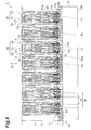
- Fig. 4 is a cross-sectional view taken along line IV-IV of the scintillator panel shown in Fig. 2 .
- the scintillator panel 1 includes a rectangular substrate 10.
- the substrate 10 has a front surface 10a and a rear surface 10b opposite to each other.
- the substrate 10 has a concavo-convex pattern Pa formed on the front surface 10a.
- a material of the substrate 10 for example, a metal such as Al, SUS (stainless steel), or the like, a resin film such as a polyimide, polyethylene terephthalate, polyethylene naphthalate, or the like, a carbon-based material such as amorphous carbon, a carbon-fiber-reinforced plastic, or the like, and a fiber optic plate (FOP: an optical device obtained by binding a plurality of optical fibers having a diameter of several microns (for example, J5734 manufactured by Hamamatsu Photonics Company Limited)) or the like, may be used.
- FOP fiber optic plate
- a high aspect resist which is also referred to as an epoxy based resin (KMPR, SU-8 or the like manufactured by Nippon Kayaku Co., Ltd), silicon, glass, and so on may be used.
- a material of a convex section constituting the concavo-convex pattern Pa may be a material having permeability with respect to scintillation light generated in a scintillator unit 20, and in this case, the scintillator panel 1 and the sensor panel having photoelectric conversion elements may be bonded at the rear surface 10b side of the substrate 10 to constitute a radiation detector.
- the concavo-convex pattern Pa may be constituted by the same scintillator material (for example, CsI (cesium iodide)) as the scintillator unit 20 (which will be described below).
- the concavo-convex pattern Pa is formed of a plurality of convex sections 11 and concave section 12 defined by the convex sections 11. That is, the plurality of convex sections 11 and concave section 12 are formed at the front surface 10a of the substrate 10.
- the convex sections 11 protrude from the front surface 10a in a predetermined direction from the rear surface 10b toward the front surface 10a of the substrate 10 (here, an incidence direction of the radiation R, and a direction perpendicular to the front surface 10a or the rear surface 10b of the substrate 10).
- Each of the convex sections 11 is formed in a rectangular parallelepiped shape.
- the convex sections 11 are periodically arranged on the front surface 10a of the substrate 10 in a two-dimensional array along an X axis and a Y axis parallel to the substrate 10 and perpendicular to each other. Accordingly, the concave section 12 defined by the convex sections 11 is groove forming a rectangular lattice shape when seen in a plan view.
- a region in which a region extending in the X-axis direction of the concave section 12 and a region extending in the Y-axis direction cross each other is referred to as a crossing region C.
- a width (a groove width) W of the concave section 12 may be about 45 to 200 ⁇ m, and when the pitch P of the convex section 11 is about 200 ⁇ m, the width W of the concave section 12 may be about 50 ⁇ m to 70 ⁇ m.
- a height H of the convex section 11 may be about 2.5 ⁇ m to 50 ⁇ m.
- the pitch P of the convex section 11 is about 200 ⁇ m
- the width W of the concave section 12 is about 70 ⁇ m
- the height H of the convex section 11 is about 15 ⁇ m.
- the scintillator panel 1 includes the plurality of scintillator units (first scintillator units) 20 formed on the convex sections 11, and scintillator units (second scintillator unit) 30 and 30a formed in the concave section 12.
- the scintillator units 20 are separated from each other (i.e., the scintillator panel 1 has a discrete type scintillator unit).
- the scintillator unit 20 may be formed by a scintillator material forming a columnar crystal, for example, referred to as CsI (cesium iodide).
- a height (a scintillator film thickness) T of the scintillator unit 20 may be, for example, about 100 ⁇ m to 600 ⁇ m.
- the scintillator units 20 extend from the convex sections 11 in a predetermined direction, and are separated from each other.
- the scintillator unit 20 has a first portion 21 and a second portion 22.
- the first portion 21 forms a rectangular shape corresponding to a shape of the convex section 11 when seen in a plan view.
- the second portion 22 forms a rectangular ring shape to cover side sections of the first portion 21 when seen in a plan view.
- the first portion 21 extends from an upper surface 11a of the convex section 11 in an incidence direction of the radiation R (a direction substantially perpendicular to the substrate 10). More specifically, the first portion 21 is constituted by a plurality of columnar crystals C1 of a scintillator material formed through crystal growth from the upper surface 11a of the convex section 11 in the incidence direction of the radiation R.
- the second portion 22 extends from a side surface 11b of the convex section 11 in the incidence direction of the radiation R to come in contact with the first portion 21.
- the second portion 22 is formed to overhang sideward from the side surface 11b of the convex section 11 and is disposed over a bottom surface of the concave section 12.
- the second portion 22 is integrally formed with the first portion 21 (adhered to the first portion 21).
- the second portion 22 is constituted by a plurality of columnar crystals C2 of a scintillator material formed through crystal growth in a direction (a direction crossing a predetermined direction) crossing the incidence direction (a direction substantially perpendicular to the substrate 10) of the radiation R from the side surface 11b of the convex section 11, and extends in the incidence direction of the radiation R as a whole.
- the columnar crystal C2 is formed at the entire side surface 11b of the convex section 11.
- the columnar crystal C1 constituting the first portion 21 forms a tapered shape having a diameter that increases away from the upper surface 11a of the convex section 11. That is, a columnar diameter of the columnar crystal C1 increases away from the upper surface 11a of the convex section 11 (i.e., from a base end section of the upper surface 11a side toward a front end section of an opposite side).
- the columnar crystal C2 constituting the second portion 22 forms a tapered shape having a diameter that increases away from the side surface 11b of the convex section 11. That is, the columnar diameter of the columnar crystal C2 increases away from the side surface 11b of the convex section 11 (i.e., from the base end section of the side surface 11b side toward the front end section of the opposite side).
- a magnification rate of the columnar diameter of the columnar crystal C2 is larger than a magnification rate of a columnar diameter R1 of the columnar crystal C1.
- the columnar diameter of the columnar crystal C2 is relatively larger than the columnar diameter of the columnar crystal C1.
- the height H of the above-mentioned convex section 11 is larger than at least the columnar diameter of the base end sections of the columnar crystal C1 constituting the first portion 21 and the columnar crystal C2 constituting the second portion 22. Accordingly, the plurality of columnar crystals C1 or columnar crystals C2 are formed on the upper surface 11a or the side surface 11b of the convex section 11.
- the second portion 22 has an upper section 22a and a lower section 22b.
- the upper section 22a is a portion of the second portion 22 closer to a front end side than a height T1 serving as an intermediate position in the height direction of the scintillator unit 20.
- the lower section 22b is a portion of the second portion 22 closer to a base end side than the height T1.
- a part of the front end side of the upper section 22a becomes a fusion-bonding section 22c.
- the fusion-bonding section 22c is a region formed by a laser beam radiated to separate the plurality of scintillator units 20 from each other, and is formed at an outer side surface of the upper section 22a.
- the fusion-bonding sections 22c are separated from each other.
- the lower sections 22b of the adjacent scintillator units 20 are separated from each other.
- the fusion-bonding sections 22c the plurality of columnar crystals C2 are fused and adhered to each other, and a columnar structure is collapsed.
- the front end section of the columnar crystal C2 is destroyed by radiation of the laser beam.
- the plurality of scintillator units 20 are separated from each other by radiation of the laser beam, and gaps S are formed between the adjacent scintillator units 20.
- the gaps S are formed by the adjacent scintillator units 20 and bottom surfaces of concave section 12.
- the gaps S have an interval D1 between the upper sections 22a opposite to each other via the gaps S, and have a larger interval D2 than the interval D 1 between the lower sections 22b opposite to each other via the gaps S.
- the gaps S have a wedge shape and an interval is increased toward the front end section of the scintillator unit 20 at a laser beam incidence position A (a position between the front end sections of the scintillator units 20). That is, the gaps S have an hourglass shape constricted at an intermediate position in the height direction (a position between the upper sections 22a opposite to each other via the gaps S) as a whole.
- the scintillator units 30 and 30a are formed in the concave section 12, in particular, on a bottom surface 12a of the concave section 12.
- the scintillator unit 30 is formed in a region different from the region corresponding to a lattice point of the lattice-shaped concave section 12 when seen in a plan view, i.e., in a region other than the crossing region C of the concave section 12.
- the scintillator unit 30a is formed in a region corresponding to the lattice point of the lattice-shaped concave section 12 when seen in a plan view, i.e., in the crossing region C of the concave section 12.
- the scintillator units 30 and 30a are integrally formed with the entire concave section 12.
- the height H1 of the scintillator unit 30 is configured to be smaller than the height H of the convex section 11.
- the height H2 of the scintillator unit 30a is configured to be larger than the height H of the convex section 11. That is, the thickness of the scintillator unit 30a is configured to be larger than the thickness of the scintillator unit 30.
- the scintillator units 30 and 30a function as a protective film configured to protect the substrate 10 from radiation of the laser beam (to be described below).
- the scintillator units 30 and 30a are constituted by a plurality of columnar crystals of a scintillator material referred to as CsI, like the first portion 21 and the second portion 22 of the scintillator unit 20.
- the columnar crystals constituting the scintillator units 30 and 30a are formed through crystal growth from the bottom surface 12a of the concave section 12 in the incidence direction of the radiation R.
- the scintillator unit 30 forms a convex shape (a substantially triangular cross-section) having a thickness that increases from corners of the concave section 12 (connecting portions between the side surfaces 11b of the convex section 11 and the bottom surface 12a of the concave section 12) toward a center in the width direction of the concave section 12.
- the scintillator unit 30a forms a convex shape (a substantially conical shape), a thickness of which is largest at the center point of the crossing region C of the concave section 12 and reduces away from the center point. Further, the scintillator units 30 and 30a may come in contact with the second portion 22 to support the columnar crystal C2 of the second portion 22 extending from the side surface 11b of the convex section 11 from the bottom surface 12a side of the concave section 12. In connection with this, the columnar diameter of the columnar crystal of the portion of the second portion 22 in contact with the scintillator unit 30 is smaller than the columnar diameter R1 of the columnar crystal C1 of the first portion 21.
- the scintillator units 30 and 30a may be partially or entirely solidified after being melted by radiation of the laser beam.
- the plurality of convex sections 11 and the concave section 12 defined by the convex sections 11 are formed on the front surface 10a of the substrate 10 (a first process).
- a base material serving as the substrate 10 is prepared, and as shown in Fig. 5 , a material of the concavo-convex pattern Pa is applied and dried on the base material.
- the concavo-convex pattern Pa is formed on the base material through photolithography to manufacture the substrate 10 having the concavo-convex pattern Pa of a predetermined dimension (the first process).
- the concavo-convex pattern Pa is formed in which the convex section 11 protrudes in a predetermined direction from the rear surface 10b of the substrate 10 toward the front surface 10a (here, an incidence direction of the radiation R and a direction perpendicular to the front surface 10a or the rear surface 10b of the substrate 10).
- the convex sections 11 are arranged in a two-dimensional array in the X-axis direction and the Y-axis direction, as shown in Fig. 6 , the concave section showing a rectangular lattice shape when seen in a plan view are formed.
- the concavo-convex pattern Pa may be formed on the base material through screen printing.
- scintillator units 40 extending in a predetermined direction from the convex sections 11 of the substrate 10 (here, in the incidence direction of the radiation R and the direction perpendicular to the front surface 10a or the rear surface 10b of the substrate 10) are formed (a second process).
- the scintillator units 30 and 30a are formed on the bottom surface 12a of the concave section 12 of the substrate 10 through crystal growth (a fourth process).
- the scintillator unit 40 is formed to include a first portion 41 having a rectangular shape to correspond to a shape of the convex section 11 when seen in a plan view, and a second portion 42 having a rectangular ring shape to cover side sections of the first portion 21 when seen in a plan view.
- the scintillator unit 40 is a portion that becomes the scintillator unit 20 (to be described below).
- the crystal of the scintillator material is grown until the scintillator unit on the upper surface 11a of the convex section 11 arrives at a predetermined height (for example, 100 ⁇ m to 600 ⁇ m). Accordingly, as shown in Fig. 7 , the plurality of scintillator units 40 separated from each other at a portion closer to the base end side than the height T1 (a portion that will become the above-mentioned lower section 22b) and in contact with each other at a portion closer to the front end side than the height T1 (a portion that will become the above-mentioned upper section 22a) are formed. As a result, the plurality of scintillator units 40 having boundary surfaces serving as contact portions 43 are formed.
- the scintillator unit 30 is formed in the concave section 12 except for the crossing region C.
- the scintillator unit 30a is formed in the concave section 12 in the crossing region C.
- the scintillator unit 30a is formed to have a larger thickness than the scintillator unit 30.
- the scintillator units 30, 30a and 40 are formed on the substrate 10 by depositing the scintillator material referred to as CsI through, for example, vacuum deposition. As various deposition conditions (a vacuum level, a deposition rate, a substrate heating temperature, an angle of a vapor flow, and so on) are controlled, the above-mentioned scintillator units 30, 30a and 40 are formed on the concavo-convex pattern Pa.
- the scintillator units 20, 30, 30a and 40 can also be formed using a vapor phase deposition method, in addition to the vacuum deposition.
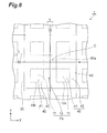
- Fig. 8 is a view showing a process of separating the scintillator units 40 using the laser beam L. As shown in Fig. 8 , as the contact portions 43 of the scintillator units 40 are scanned with the laser beam L in the X-axis direction and the Y-axis direction, the laser beam L is radiated to the contact portions 43 of the scintillator units 40 extending from the adjacent convex sections 11.
- a part of the second portion 42 of the scintillator unit 40 is cut and removed by radiation of the laser beam L to separate the scintillator units 40 from each other.
- the laser beam L is radiated two times.
- the contact portions 43 of the scintillator units 40 as the laser beam L is radiated, the plurality of columnar crystals C2 are fused and adhered to each other. Accordingly, the fusion-bonding section 22c is formed at a part of the second portion 42 of the scintillator unit 40. In this way, as the laser beam L is radiated to separate the plurality of scintillator units 40 from each other, the scintillator units 20 are formed and the scintillator panel 1 is manufactured.
- a laser beam having a wavelength of 515 nm, a pulse having a width of 1 ps and a cyclic frequency of 20 kHz and obtained through second harmonic generation (SHG), or a laser beam having a wavelength of 258 nm, a pulse having a width of 1 ps and a cyclic frequency of 20 kHz and obtained through fourth harmonic generation (SHG) may be used.
- the scintillator units 20 formed through crystal growth can be spaced apart from each other (i.e., pixelation of the scintillator units can be realized). Since the crystal growth is performed in a state in which the lower sections 22b of the scintillator units 20 are spaced apart from each other, when scanning with the laser beam is performed, the laser beam is radiated to only a part of the upper sections 22a of the adjacent scintillator units 20.
- the scintillator units 40 extending from the convex sections 11 of the substrate 10 in the predetermined direction are formed. For this reason, the scintillator units 40 are formed to be separated from each other by the predetermined height with the upper surface 11a of the convex section 11 as the origin, and in contact with each other from the predetermined height to over the concave section 12.
- the scintillator units 20 having an increased thickness are obtained.
- the laser beam may be preferably radiated to only the contact portion 43, deterioration of the crystal can be suppressed.
- the scintillator unit 30 formed on the bottom surface 12a of the concave section 12 functions as a protective film, for example, when the substrate 10 is the sensor panel, damage to interconnections or the like installed on the sensor panel when the laser beam L is radiated can be prevented.
- the scintillator unit 30a having a relatively large thickness functions as the protective film in the crossing region C of the concave section 12 to which the laser beam L is radiated twice, damage to the interconnections or the like installed on the substrate (the sensor panel) 10 can be more securely prevented.
- the aspect of the present invention may be applied to the radiation detector including the above-mentioned scintillator panel or the like.
- the radiation detector may include the above-mentioned scintillator panel 1
- the substrate 10 may be the sensor panel (the TFT panel or the CMOS image sensor panel) including the plurality of photoelectric conversion elements arranged to optically couple to the scintillator unit 20.
- the convex sections 11 corresponding to the pixels of the TFT panel or the CMOS image sensor serving as the substrate 10 are formed, and the scintillator units 20 and 30 are formed thereon.
- the material of the convex section 11 and the method of forming the same are as described above.
- the convex sections 11 may be constituted by the material having permeability with respect to the scintillation light generated in the scintillator unit 20.
- the above-mentioned scintillator panel 1 since the above-mentioned scintillator panel 1 is provided, characteristics can be improved.
- the substrate 10 is the sensor panel including the photoelectric conversion elements, when the convex section 11 is directly formed on the photoelectric conversion elements to form the scintillator unit 20, there is no need to stick the scintillator panel and the sensor panel, which are separately prepared, together.
Landscapes
- Physics & Mathematics (AREA)
- High Energy & Nuclear Physics (AREA)
- Health & Medical Sciences (AREA)
- Chemical & Material Sciences (AREA)
- Life Sciences & Earth Sciences (AREA)
- General Physics & Mathematics (AREA)
- Crystallography & Structural Chemistry (AREA)
- Molecular Biology (AREA)
- Spectroscopy & Molecular Physics (AREA)
- Engineering & Computer Science (AREA)
- General Engineering & Computer Science (AREA)
- Measurement Of Radiation (AREA)
- Conversion Of X-Rays Into Visible Images (AREA)
Priority Applications (1)
| Application Number | Priority Date | Filing Date | Title |
|---|---|---|---|
| EP17175327.0A EP3240031B1 (de) | 2013-01-09 | 2013-11-05 | Szintillatortafel und strahlungsdetektor |
Applications Claiming Priority (2)
| Application Number | Priority Date | Filing Date | Title |
|---|---|---|---|
| JP2013001908A JP6133059B2 (ja) | 2013-01-09 | 2013-01-09 | シンチレータパネルの製造方法、シンチレータパネル、及び放射線検出器 |
| PCT/JP2013/079914 WO2014109116A1 (ja) | 2013-01-09 | 2013-11-05 | シンチレータパネルの製造方法、シンチレータパネル、及び放射線検出器 |
Related Child Applications (2)
| Application Number | Title | Priority Date | Filing Date |
|---|---|---|---|
| EP17175327.0A Division EP3240031B1 (de) | 2013-01-09 | 2013-11-05 | Szintillatortafel und strahlungsdetektor |
| EP17175327.0A Division-Into EP3240031B1 (de) | 2013-01-09 | 2013-11-05 | Szintillatortafel und strahlungsdetektor |
Publications (3)
| Publication Number | Publication Date |
|---|---|
| EP2945166A1 true EP2945166A1 (de) | 2015-11-18 |
| EP2945166A4 EP2945166A4 (de) | 2016-07-20 |
| EP2945166B1 EP2945166B1 (de) | 2018-02-28 |
Family
ID=51166781
Family Applications (2)
| Application Number | Title | Priority Date | Filing Date |
|---|---|---|---|
| EP17175327.0A Active EP3240031B1 (de) | 2013-01-09 | 2013-11-05 | Szintillatortafel und strahlungsdetektor |
| EP13871088.4A Active EP2945166B1 (de) | 2013-01-09 | 2013-11-05 | Herstellungsverfahren für szintillatortafel und strahlungsdetektor |
Family Applications Before (1)
| Application Number | Title | Priority Date | Filing Date |
|---|---|---|---|
| EP17175327.0A Active EP3240031B1 (de) | 2013-01-09 | 2013-11-05 | Szintillatortafel und strahlungsdetektor |
Country Status (6)
| Country | Link |
|---|---|
| US (1) | US9405020B2 (de) |
| EP (2) | EP3240031B1 (de) |
| JP (1) | JP6133059B2 (de) |
| KR (1) | KR102059230B1 (de) |
| CN (1) | CN104903971B (de) |
| WO (1) | WO2014109116A1 (de) |
Cited By (1)
| Publication number | Priority date | Publication date | Assignee | Title |
|---|---|---|---|---|
| EP2896974A4 (de) * | 2012-09-14 | 2016-05-18 | Hamamatsu Photonics Kk | Szintillatortafel und strahlungsmesser |
Families Citing this family (2)
| Publication number | Priority date | Publication date | Assignee | Title |
|---|---|---|---|---|
| JP6951092B2 (ja) * | 2017-03-17 | 2021-10-20 | キヤノンメディカルシステムズ株式会社 | 放射線検出器、シンチレータアレイ、及びシンチレータアレイの製造方法 |
| CN110368014B (zh) * | 2019-07-19 | 2023-10-31 | 沈阳智核医疗科技有限公司 | 用于pet探测器的晶体阵列、探测器环和pet探测器 |
Family Cites Families (16)
| Publication number | Priority date | Publication date | Assignee | Title |
|---|---|---|---|---|
| JP2547908Y2 (ja) | 1990-08-08 | 1997-09-17 | 株式会社シライ | ハンガー |
| US5229613A (en) * | 1991-09-06 | 1993-07-20 | Horiba Instruments, Incorporated | Extended lifetime scintillation camera plate assembly |
| JP2547908B2 (ja) * | 1991-10-02 | 1996-10-30 | 浜松ホトニクス株式会社 | 放射線検出装置 |
| JPH09325185A (ja) * | 1996-06-03 | 1997-12-16 | Toshiba Fa Syst Eng Kk | 放射線検出器とその製造方法と透視検査装置とctスキャナ |
| JP3551851B2 (ja) * | 1999-08-24 | 2004-08-11 | 松下電器産業株式会社 | X線蛍光体製作方法及びx線蛍光体形成用基板 |
| WO2003019599A1 (en) * | 2001-08-29 | 2003-03-06 | Kabushiki Kaisha Toshiba | Production method and production device for x-ray image detector, and x-ray image detector |
| JP2003167060A (ja) | 2001-11-30 | 2003-06-13 | Toshiba Corp | X線平面検出器 |
| US6921909B2 (en) * | 2002-08-27 | 2005-07-26 | Radiation Monitoring Devices, Inc. | Pixellated micro-columnar films scintillator |
| JP2004108806A (ja) * | 2002-09-13 | 2004-04-08 | Fuji Photo Film Co Ltd | 放射線像変換パネル |
| JP4498283B2 (ja) * | 2006-01-30 | 2010-07-07 | キヤノン株式会社 | 撮像装置、放射線撮像装置及びこれらの製造方法 |
| JP2011017683A (ja) * | 2009-07-10 | 2011-01-27 | Fujifilm Corp | 放射線画像検出器及びその製造方法 |
| JP2012154696A (ja) * | 2011-01-24 | 2012-08-16 | Canon Inc | シンチレータパネル、放射線検出装置およびそれらの製造方法 |
| JP2012154811A (ja) * | 2011-01-26 | 2012-08-16 | Canon Inc | シンチレータパネルおよびその製造方法ならびに放射線検出装置 |
| JP2013050364A (ja) * | 2011-08-30 | 2013-03-14 | Fujifilm Corp | 放射線画像検出装置 |
| JP6018854B2 (ja) * | 2012-09-14 | 2016-11-02 | 浜松ホトニクス株式会社 | シンチレータパネル、及び、放射線検出器 |
| JP6032236B2 (ja) * | 2014-04-08 | 2016-11-24 | トヨタ自動車株式会社 | レーザ溶接方法および溶接構造 |
-
2013
- 2013-01-09 JP JP2013001908A patent/JP6133059B2/ja active Active
- 2013-11-05 WO PCT/JP2013/079914 patent/WO2014109116A1/ja not_active Ceased
- 2013-11-05 KR KR1020157018040A patent/KR102059230B1/ko active Active
- 2013-11-05 US US14/759,739 patent/US9405020B2/en active Active
- 2013-11-05 EP EP17175327.0A patent/EP3240031B1/de active Active
- 2013-11-05 CN CN201380070006.XA patent/CN104903971B/zh active Active
- 2013-11-05 EP EP13871088.4A patent/EP2945166B1/de active Active
Cited By (1)
| Publication number | Priority date | Publication date | Assignee | Title |
|---|---|---|---|---|
| EP2896974A4 (de) * | 2012-09-14 | 2016-05-18 | Hamamatsu Photonics Kk | Szintillatortafel und strahlungsmesser |
Also Published As
| Publication number | Publication date |
|---|---|
| US9405020B2 (en) | 2016-08-02 |
| EP3240031A1 (de) | 2017-11-01 |
| CN104903971B (zh) | 2017-08-18 |
| EP2945166B1 (de) | 2018-02-28 |
| EP3240031B1 (de) | 2019-07-10 |
| KR20150103042A (ko) | 2015-09-09 |
| EP2945166A4 (de) | 2016-07-20 |
| JP2014134430A (ja) | 2014-07-24 |
| WO2014109116A1 (ja) | 2014-07-17 |
| CN104903971A (zh) | 2015-09-09 |
| JP6133059B2 (ja) | 2017-05-24 |
| KR102059230B1 (ko) | 2019-12-24 |
| US20150355342A1 (en) | 2015-12-10 |
Similar Documents
| Publication | Publication Date | Title |
|---|---|---|
| US9054012B2 (en) | Radiation detection apparatus and method of manufacturing the same | |
| US9360566B2 (en) | Radiation detector | |
| EP3937246B1 (de) | Linsenfolie, linsenfolieneinheit, bildgebungsmodul, bildgebungsvorrichtung | |
| JP6018854B2 (ja) | シンチレータパネル、及び、放射線検出器 | |
| US9322932B2 (en) | Scintillator panel and radiation detection device | |
| JP2012045099A (ja) | 放射線画像撮影用グリッド及びその製造方法、並びに放射線画像撮影システム | |
| EP2945166B1 (de) | Herstellungsverfahren für szintillatortafel und strahlungsdetektor | |
| JP2017181295A (ja) | 放射線検出器及びシンチレータパネル | |
| KR20180092938A (ko) | 신틸레이터 패널 및 방사선 검출기 | |
| EP3394641B1 (de) | Szintillator, szintillatorbaugruppe, röntgendetektor und röntgenbildgebungssystem und verfahren zur herstellung eines szintillators | |
| JP5028048B2 (ja) | 撮像装置 | |
| CN116635751B (zh) | 放射线检测器、放射线检测器的制造方法和闪烁体面板组件 | |
| CN104124254A (zh) | 放射线摄像装置及其制造方法以及放射线检查装置 | |
| CN116724252B (zh) | 放射线检测器和放射线检测器的制造方法 | |
| WO2018020555A1 (ja) | シンチレータセンサ基板及びシンチレータセンサ基板の製造方法 | |
| US20250180759A1 (en) | Scintillator panel, radiation detector, method for manufacturing scintillator panel, and method for manufacturing radiation detector | |
| JP6579856B2 (ja) | 放射線撮像装置及びその製造方法並びに放射線撮像システム | |
| TW202142893A (zh) | 放射線檢測器及放射線檢測器的製造方法 |
Legal Events
| Date | Code | Title | Description |
|---|---|---|---|
| PUAI | Public reference made under article 153(3) epc to a published international application that has entered the european phase |
Free format text: ORIGINAL CODE: 0009012 |
|
| 17P | Request for examination filed |
Effective date: 20150625 |
|
| AK | Designated contracting states |
Kind code of ref document: A1 Designated state(s): AL AT BE BG CH CY CZ DE DK EE ES FI FR GB GR HR HU IE IS IT LI LT LU LV MC MK MT NL NO PL PT RO RS SE SI SK SM TR |
|
| AX | Request for extension of the european patent |
Extension state: BA ME |
|
| DAX | Request for extension of the european patent (deleted) | ||
| REG | Reference to a national code |
Ref country code: DE Ref legal event code: R079 Ref document number: 602013033877 Country of ref document: DE Free format text: PREVIOUS MAIN CLASS: G21K0004000000 Ipc: H01L0027146000 |
|
| A4 | Supplementary search report drawn up and despatched |
Effective date: 20160621 |
|
| RIC1 | Information provided on ipc code assigned before grant |
Ipc: G01T 1/202 20060101ALI20160615BHEP Ipc: H01L 27/146 20060101AFI20160615BHEP Ipc: G21K 4/00 20060101ALI20160615BHEP |
|
| 17Q | First examination report despatched |
Effective date: 20170407 |
|
| GRAP | Despatch of communication of intention to grant a patent |
Free format text: ORIGINAL CODE: EPIDOSNIGR1 |
|
| INTG | Intention to grant announced |
Effective date: 20170915 |
|
| GRAS | Grant fee paid |
Free format text: ORIGINAL CODE: EPIDOSNIGR3 |
|
| GRAA | (expected) grant |
Free format text: ORIGINAL CODE: 0009210 |
|
| AK | Designated contracting states |
Kind code of ref document: B1 Designated state(s): AL AT BE BG CH CY CZ DE DK EE ES FI FR GB GR HR HU IE IS IT LI LT LU LV MC MK MT NL NO PL PT RO RS SE SI SK SM TR |
|
| REG | Reference to a national code |
Ref country code: GB Ref legal event code: FG4D Ref country code: CH Ref legal event code: EP |
|
| REG | Reference to a national code |
Ref country code: AT Ref legal event code: REF Ref document number: 975023 Country of ref document: AT Kind code of ref document: T Effective date: 20180315 |
|
| REG | Reference to a national code |
Ref country code: IE Ref legal event code: FG4D |
|
| REG | Reference to a national code |
Ref country code: DE Ref legal event code: R096 Ref document number: 602013033877 Country of ref document: DE |
|
| REG | Reference to a national code |
Ref country code: NL Ref legal event code: FP |
|
| REG | Reference to a national code |
Ref country code: LT Ref legal event code: MG4D |
|
| REG | Reference to a national code |
Ref country code: AT Ref legal event code: MK05 Ref document number: 975023 Country of ref document: AT Kind code of ref document: T Effective date: 20180228 |
|
| PG25 | Lapsed in a contracting state [announced via postgrant information from national office to epo] |
Ref country code: ES Free format text: LAPSE BECAUSE OF FAILURE TO SUBMIT A TRANSLATION OF THE DESCRIPTION OR TO PAY THE FEE WITHIN THE PRESCRIBED TIME-LIMIT Effective date: 20180228 Ref country code: LT Free format text: LAPSE BECAUSE OF FAILURE TO SUBMIT A TRANSLATION OF THE DESCRIPTION OR TO PAY THE FEE WITHIN THE PRESCRIBED TIME-LIMIT Effective date: 20180228 Ref country code: NO Free format text: LAPSE BECAUSE OF FAILURE TO SUBMIT A TRANSLATION OF THE DESCRIPTION OR TO PAY THE FEE WITHIN THE PRESCRIBED TIME-LIMIT Effective date: 20180528 Ref country code: HR Free format text: LAPSE BECAUSE OF FAILURE TO SUBMIT A TRANSLATION OF THE DESCRIPTION OR TO PAY THE FEE WITHIN THE PRESCRIBED TIME-LIMIT Effective date: 20180228 Ref country code: CY Free format text: LAPSE BECAUSE OF FAILURE TO SUBMIT A TRANSLATION OF THE DESCRIPTION OR TO PAY THE FEE WITHIN THE PRESCRIBED TIME-LIMIT Effective date: 20180228 Ref country code: FI Free format text: LAPSE BECAUSE OF FAILURE TO SUBMIT A TRANSLATION OF THE DESCRIPTION OR TO PAY THE FEE WITHIN THE PRESCRIBED TIME-LIMIT Effective date: 20180228 |
|
| PG25 | Lapsed in a contracting state [announced via postgrant information from national office to epo] |
Ref country code: GR Free format text: LAPSE BECAUSE OF FAILURE TO SUBMIT A TRANSLATION OF THE DESCRIPTION OR TO PAY THE FEE WITHIN THE PRESCRIBED TIME-LIMIT Effective date: 20180529 Ref country code: AT Free format text: LAPSE BECAUSE OF FAILURE TO SUBMIT A TRANSLATION OF THE DESCRIPTION OR TO PAY THE FEE WITHIN THE PRESCRIBED TIME-LIMIT Effective date: 20180228 Ref country code: LV Free format text: LAPSE BECAUSE OF FAILURE TO SUBMIT A TRANSLATION OF THE DESCRIPTION OR TO PAY THE FEE WITHIN THE PRESCRIBED TIME-LIMIT Effective date: 20180228 Ref country code: SE Free format text: LAPSE BECAUSE OF FAILURE TO SUBMIT A TRANSLATION OF THE DESCRIPTION OR TO PAY THE FEE WITHIN THE PRESCRIBED TIME-LIMIT Effective date: 20180228 Ref country code: BG Free format text: LAPSE BECAUSE OF FAILURE TO SUBMIT A TRANSLATION OF THE DESCRIPTION OR TO PAY THE FEE WITHIN THE PRESCRIBED TIME-LIMIT Effective date: 20180528 Ref country code: RS Free format text: LAPSE BECAUSE OF FAILURE TO SUBMIT A TRANSLATION OF THE DESCRIPTION OR TO PAY THE FEE WITHIN THE PRESCRIBED TIME-LIMIT Effective date: 20180228 |
|
| REG | Reference to a national code |
Ref country code: FR Ref legal event code: PLFP Year of fee payment: 6 |
|
| PG25 | Lapsed in a contracting state [announced via postgrant information from national office to epo] |
Ref country code: RO Free format text: LAPSE BECAUSE OF FAILURE TO SUBMIT A TRANSLATION OF THE DESCRIPTION OR TO PAY THE FEE WITHIN THE PRESCRIBED TIME-LIMIT Effective date: 20180228 Ref country code: IT Free format text: LAPSE BECAUSE OF FAILURE TO SUBMIT A TRANSLATION OF THE DESCRIPTION OR TO PAY THE FEE WITHIN THE PRESCRIBED TIME-LIMIT Effective date: 20180228 Ref country code: PL Free format text: LAPSE BECAUSE OF FAILURE TO SUBMIT A TRANSLATION OF THE DESCRIPTION OR TO PAY THE FEE WITHIN THE PRESCRIBED TIME-LIMIT Effective date: 20180228 Ref country code: AL Free format text: LAPSE BECAUSE OF FAILURE TO SUBMIT A TRANSLATION OF THE DESCRIPTION OR TO PAY THE FEE WITHIN THE PRESCRIBED TIME-LIMIT Effective date: 20180228 Ref country code: EE Free format text: LAPSE BECAUSE OF FAILURE TO SUBMIT A TRANSLATION OF THE DESCRIPTION OR TO PAY THE FEE WITHIN THE PRESCRIBED TIME-LIMIT Effective date: 20180228 |
|
| REG | Reference to a national code |
Ref country code: DE Ref legal event code: R097 Ref document number: 602013033877 Country of ref document: DE |
|
| PG25 | Lapsed in a contracting state [announced via postgrant information from national office to epo] |
Ref country code: DK Free format text: LAPSE BECAUSE OF FAILURE TO SUBMIT A TRANSLATION OF THE DESCRIPTION OR TO PAY THE FEE WITHIN THE PRESCRIBED TIME-LIMIT Effective date: 20180228 Ref country code: SM Free format text: LAPSE BECAUSE OF FAILURE TO SUBMIT A TRANSLATION OF THE DESCRIPTION OR TO PAY THE FEE WITHIN THE PRESCRIBED TIME-LIMIT Effective date: 20180228 Ref country code: CZ Free format text: LAPSE BECAUSE OF FAILURE TO SUBMIT A TRANSLATION OF THE DESCRIPTION OR TO PAY THE FEE WITHIN THE PRESCRIBED TIME-LIMIT Effective date: 20180228 Ref country code: SK Free format text: LAPSE BECAUSE OF FAILURE TO SUBMIT A TRANSLATION OF THE DESCRIPTION OR TO PAY THE FEE WITHIN THE PRESCRIBED TIME-LIMIT Effective date: 20180228 |
|
| PLBE | No opposition filed within time limit |
Free format text: ORIGINAL CODE: 0009261 |
|
| STAA | Information on the status of an ep patent application or granted ep patent |
Free format text: STATUS: NO OPPOSITION FILED WITHIN TIME LIMIT |
|
| 26N | No opposition filed |
Effective date: 20181129 |
|
| PG25 | Lapsed in a contracting state [announced via postgrant information from national office to epo] |
Ref country code: SI Free format text: LAPSE BECAUSE OF FAILURE TO SUBMIT A TRANSLATION OF THE DESCRIPTION OR TO PAY THE FEE WITHIN THE PRESCRIBED TIME-LIMIT Effective date: 20180228 |
|
| REG | Reference to a national code |
Ref country code: DE Ref legal event code: R119 Ref document number: 602013033877 Country of ref document: DE |
|
| REG | Reference to a national code |
Ref country code: CH Ref legal event code: PL |
|
| PG25 | Lapsed in a contracting state [announced via postgrant information from national office to epo] |
Ref country code: LU Free format text: LAPSE BECAUSE OF NON-PAYMENT OF DUE FEES Effective date: 20181105 Ref country code: MC Free format text: LAPSE BECAUSE OF FAILURE TO SUBMIT A TRANSLATION OF THE DESCRIPTION OR TO PAY THE FEE WITHIN THE PRESCRIBED TIME-LIMIT Effective date: 20180228 |
|
| REG | Reference to a national code |
Ref country code: BE Ref legal event code: MM Effective date: 20181130 |
|
| REG | Reference to a national code |
Ref country code: IE Ref legal event code: MM4A |
|
| PG25 | Lapsed in a contracting state [announced via postgrant information from national office to epo] |
Ref country code: CH Free format text: LAPSE BECAUSE OF NON-PAYMENT OF DUE FEES Effective date: 20181130 Ref country code: LI Free format text: LAPSE BECAUSE OF NON-PAYMENT OF DUE FEES Effective date: 20181130 |
|
| PG25 | Lapsed in a contracting state [announced via postgrant information from national office to epo] |
Ref country code: DE Free format text: LAPSE BECAUSE OF NON-PAYMENT OF DUE FEES Effective date: 20190601 Ref country code: IE Free format text: LAPSE BECAUSE OF NON-PAYMENT OF DUE FEES Effective date: 20181105 |
|
| PG25 | Lapsed in a contracting state [announced via postgrant information from national office to epo] |
Ref country code: BE Free format text: LAPSE BECAUSE OF NON-PAYMENT OF DUE FEES Effective date: 20181130 |
|
| PG25 | Lapsed in a contracting state [announced via postgrant information from national office to epo] |
Ref country code: MT Free format text: LAPSE BECAUSE OF NON-PAYMENT OF DUE FEES Effective date: 20181105 |
|
| PG25 | Lapsed in a contracting state [announced via postgrant information from national office to epo] |
Ref country code: TR Free format text: LAPSE BECAUSE OF FAILURE TO SUBMIT A TRANSLATION OF THE DESCRIPTION OR TO PAY THE FEE WITHIN THE PRESCRIBED TIME-LIMIT Effective date: 20180228 |
|
| PG25 | Lapsed in a contracting state [announced via postgrant information from national office to epo] |
Ref country code: PT Free format text: LAPSE BECAUSE OF FAILURE TO SUBMIT A TRANSLATION OF THE DESCRIPTION OR TO PAY THE FEE WITHIN THE PRESCRIBED TIME-LIMIT Effective date: 20180228 |
|
| PG25 | Lapsed in a contracting state [announced via postgrant information from national office to epo] |
Ref country code: MK Free format text: LAPSE BECAUSE OF NON-PAYMENT OF DUE FEES Effective date: 20180228 Ref country code: HU Free format text: LAPSE BECAUSE OF FAILURE TO SUBMIT A TRANSLATION OF THE DESCRIPTION OR TO PAY THE FEE WITHIN THE PRESCRIBED TIME-LIMIT; INVALID AB INITIO Effective date: 20131105 |
|
| PG25 | Lapsed in a contracting state [announced via postgrant information from national office to epo] |
Ref country code: IS Free format text: LAPSE BECAUSE OF FAILURE TO SUBMIT A TRANSLATION OF THE DESCRIPTION OR TO PAY THE FEE WITHIN THE PRESCRIBED TIME-LIMIT Effective date: 20180628 |
|
| P01 | Opt-out of the competence of the unified patent court (upc) registered |
Effective date: 20230509 |
|
| PGFP | Annual fee paid to national office [announced via postgrant information from national office to epo] |
Ref country code: NL Payment date: 20241004 Year of fee payment: 12 |
|
| PGFP | Annual fee paid to national office [announced via postgrant information from national office to epo] |
Ref country code: GB Payment date: 20241001 Year of fee payment: 12 |
|
| PGFP | Annual fee paid to national office [announced via postgrant information from national office to epo] |
Ref country code: FR Payment date: 20241001 Year of fee payment: 12 |