EP2940739B1 - Hybrider, integrierter optoelektronischer silica-auf-silicium-chip und herstellungsverfahren dafür - Google Patents
Hybrider, integrierter optoelektronischer silica-auf-silicium-chip und herstellungsverfahren dafür Download PDFInfo
- Publication number
- EP2940739B1 EP2940739B1 EP13867481.7A EP13867481A EP2940739B1 EP 2940739 B1 EP2940739 B1 EP 2940739B1 EP 13867481 A EP13867481 A EP 13867481A EP 2940739 B1 EP2940739 B1 EP 2940739B1
- Authority
- EP
- European Patent Office
- Prior art keywords
- silica
- optoelectronic chip
- lug boss
- layer
- waveguide
- Prior art date
- Legal status (The legal status is an assumption and is not a legal conclusion. Google has not performed a legal analysis and makes no representation as to the accuracy of the status listed.)
- Active
Links
Images


Classifications
-
- G—PHYSICS
- G02—OPTICS
- G02B—OPTICAL ELEMENTS, SYSTEMS OR APPARATUS
- G02B6/00—Light guides; Structural details of arrangements comprising light guides and other optical elements, e.g. couplings
- G02B6/24—Coupling light guides
- G02B6/42—Coupling light guides with opto-electronic elements
- G02B6/4201—Packages, e.g. shape, construction, internal or external details
- G02B6/4256—Details of housings
- G02B6/4257—Details of housings having a supporting carrier or a mounting substrate or a mounting plate
-
- G—PHYSICS
- G02—OPTICS
- G02B—OPTICAL ELEMENTS, SYSTEMS OR APPARATUS
- G02B6/00—Light guides; Structural details of arrangements comprising light guides and other optical elements, e.g. couplings
- G02B6/24—Coupling light guides
- G02B6/42—Coupling light guides with opto-electronic elements
-
- G—PHYSICS
- G02—OPTICS
- G02B—OPTICAL ELEMENTS, SYSTEMS OR APPARATUS
- G02B6/00—Light guides; Structural details of arrangements comprising light guides and other optical elements, e.g. couplings
- G02B6/10—Light guides; Structural details of arrangements comprising light guides and other optical elements, e.g. couplings of the optical waveguide type
- G02B6/12—Light guides; Structural details of arrangements comprising light guides and other optical elements, e.g. couplings of the optical waveguide type of the integrated circuit kind
- G02B6/122—Basic optical elements, e.g. light-guiding paths
-
- G—PHYSICS
- G02—OPTICS
- G02B—OPTICAL ELEMENTS, SYSTEMS OR APPARATUS
- G02B6/00—Light guides; Structural details of arrangements comprising light guides and other optical elements, e.g. couplings
- G02B6/24—Coupling light guides
- G02B6/26—Optical coupling means
- G02B6/30—Optical coupling means for use between fibre and thin-film device
- G02B6/305—Optical coupling means for use between fibre and thin-film device and having an integrated mode-size expanding section, e.g. tapered waveguide
-
- G—PHYSICS
- G02—OPTICS
- G02B—OPTICAL ELEMENTS, SYSTEMS OR APPARATUS
- G02B6/00—Light guides; Structural details of arrangements comprising light guides and other optical elements, e.g. couplings
- G02B6/24—Coupling light guides
- G02B6/42—Coupling light guides with opto-electronic elements
- G02B6/4201—Packages, e.g. shape, construction, internal or external details
- G02B6/4219—Mechanical fixtures for holding or positioning the elements relative to each other in the couplings; Alignment methods for the elements, e.g. measuring or observing methods especially used therefor
- G02B6/422—Active alignment, i.e. moving the elements in response to the detected degree of coupling or position of the elements
- G02B6/4221—Active alignment, i.e. moving the elements in response to the detected degree of coupling or position of the elements involving a visual detection of the position of the elements, e.g. by using a microscope or a camera
- G02B6/4224—Active alignment, i.e. moving the elements in response to the detected degree of coupling or position of the elements involving a visual detection of the position of the elements, e.g. by using a microscope or a camera using visual alignment markings, e.g. index methods
-
- G—PHYSICS
- G02—OPTICS
- G02B—OPTICAL ELEMENTS, SYSTEMS OR APPARATUS
- G02B6/00—Light guides; Structural details of arrangements comprising light guides and other optical elements, e.g. couplings
- G02B6/24—Coupling light guides
- G02B6/42—Coupling light guides with opto-electronic elements
- G02B6/4201—Packages, e.g. shape, construction, internal or external details
- G02B6/4219—Mechanical fixtures for holding or positioning the elements relative to each other in the couplings; Alignment methods for the elements, e.g. measuring or observing methods especially used therefor
- G02B6/4228—Passive alignment, i.e. without a detection of the degree of coupling or the position of the elements
- G02B6/4232—Passive alignment, i.e. without a detection of the degree of coupling or the position of the elements using the surface tension of fluid solder to align the elements, e.g. solder bump techniques
-
- H—ELECTRICITY
- H10—SEMICONDUCTOR DEVICES; ELECTRIC SOLID-STATE DEVICES NOT OTHERWISE PROVIDED FOR
- H10F—INORGANIC SEMICONDUCTOR DEVICES SENSITIVE TO INFRARED RADIATION, LIGHT, ELECTROMAGNETIC RADIATION OF SHORTER WAVELENGTH OR CORPUSCULAR RADIATION
- H10F55/00—Radiation-sensitive semiconductor devices covered by groups H10F10/00, H10F19/00 or H10F30/00 being structurally associated with electric light sources and electrically or optically coupled thereto
-
- H—ELECTRICITY
- H10—SEMICONDUCTOR DEVICES; ELECTRIC SOLID-STATE DEVICES NOT OTHERWISE PROVIDED FOR
- H10F—INORGANIC SEMICONDUCTOR DEVICES SENSITIVE TO INFRARED RADIATION, LIGHT, ELECTROMAGNETIC RADIATION OF SHORTER WAVELENGTH OR CORPUSCULAR RADIATION
- H10F71/00—Manufacture or treatment of devices covered by this subclass
-
- H—ELECTRICITY
- H10—SEMICONDUCTOR DEVICES; ELECTRIC SOLID-STATE DEVICES NOT OTHERWISE PROVIDED FOR
- H10F—INORGANIC SEMICONDUCTOR DEVICES SENSITIVE TO INFRARED RADIATION, LIGHT, ELECTROMAGNETIC RADIATION OF SHORTER WAVELENGTH OR CORPUSCULAR RADIATION
- H10F77/00—Constructional details of devices covered by this subclass
- H10F77/40—Optical elements or arrangements
- H10F77/413—Optical elements or arrangements directly associated or integrated with the devices, e.g. back reflectors
Definitions
- the invention relates to the technical field of photon integrated devices, specifically to a silica-on-silicon-based hybrid integrated optoelectronic chip and a manufacturing method therefor, and can be applied in combining of output light from a plurality of lasers or in spectroscopic exploration of a multi-wavelength light source.
- lasers based on III-V material such as InP, GaAs, etc.
- electro-absorption modulated lasers have been developed from chip research to mass production, the encapsulated devices of which have been applied, as mature light sources, to optoelectronic fields such as optical communication, optical medical treatment, etc., and the speed of the devices ranges from hundreds of megabits per second to tens of gigabits per second.
- Passive waveguide material includes a plurality of materials such as silica, silica-on-silicon, silicon-on-insulator, etc.
- the problem to be solved by the invention is to provide a silica-on-silicon-based hybrid integrated optoelectronic chip and a manufacturing method therefor.
- Mature silicon-material process is used by the hybrid integrated chip, lug bosses, a groove and silica waveguide structures with high refractive index on a silicon substrate are designed, and alignment coupling is easily achieved.
- a high-frequency electrode is manufactured and a solder bumps structure is flip bonded under the lug bosses of the invention, both the high-frequency signals can be transmitted and the direct-current driving signals can be loaded and accurate alignment can be achieved by the active optoelectronic chip.
- the present teaching provides a silica-on-silicon-based hybrid integrated optoelectronic chip as detailed in claim 1. Also provided is a method according to claim 6. Advantageous features are provided in dependent claims.
- a first aspect of the invention provides a silica-on-silicon-based hybrid integrated optoelectronic chip, comprising a silicon substrate (1), the surface of the silicon substrate is provided with a platform (8), lug bosses (6, 7) and a groove (10), a silica waveguide element (2) is arranged in the groove, the lug bosses protrude from a surface of the platform, the surface of the platform is provided with a discontinuous metal electrode layer (3), the surface of the metal electrode layer is provided with solder bumps (4), and an active optoelectronic chip (5) is arranged above the solder bumps and the lug bosses, and wherein the protruding lug bosses (6, 7) comprise a horizontal alignment lug boss (6) and a vertical alignment lug boss (7), the height of the horizontal alignment lug boss being equal to that of the vertical alignment lug boss, both of which being 10 ⁇ m-100 ⁇ m.
- a further aspect of the invention provides a manufacturing method for a silica-on-silicon-based hybrid integrated optoelectronic chip, comprising the following steps: manufacturing a silicon substrate (1); manufacturing a horizontal alignment lug boss (6) and a vertical alignment lug boss (7) on a surface of the silicon substrate (1), the height of the horizontal alignment lug boss being equal to that of the vertical alignment lug boss, both of which being 10 ⁇ m-100 ⁇ m; manufacturing a groove (10) on one side of the lug bosses on the silicon substrate; arranging a silica waveguide element (2) in the groove (10) of the silicon substrate using a silica thermal bonding process; manufacturing a discontinuous metal electrode layer (3) on the silicon substrate; manufacturing solder bumps (4) above a direct-current electrode area (25) and an alternating-current electrode area (26) of the metal electrode layer; soldering an active optoelectronic chip (5) above the solder bumps, the vertical alignment lug boss (7) and the horizontal alignment lug boss (6).
- the step 1 includes a few steps below when the silica growth process is used in manufacturing the silica waveguide element:
- a silica-on-silicon-based hybrid integrated optoelectronic chip and a manufacturing method therefor are provided by the invention, and multi-step processes including material growth, hot oxygen bonding, flip-chip bonding, photo etching alignment and the like are used, thereby guaranteeing high-efficiency light coupling among waveguide devices of different materials, and reducing light reflection between waveguide end faces.
- a high-frequency electrode is manufactured between the horizontal and vertical alignment lug bosses, and due to the fact that flip-chip bonding technology is beneficial to the transmission of high-frequency signals, the integration level between devices is improved.
- the process design not only can achieve chip-level probe testing, but also can be used for subsequent gold ball bonding or wedge bonding processes, thereby facilitating the achievement of encapsulation and mass production of hybrid integrated chips.
- a silica-on-silicon-based hybrid integrated optoelectronic chip is provided by the invention, the structure of which comprises a silicon substrate 1, which is a silicon substrate of a silicon-based waveguide structure and the surface of which is provided with a platform 8, a groove 10 and a plurality of lug bosses, wherein the lug bosses are of lug boss structures that are protruded from the surface of the platform 8, and the groove is of a groove structure that is concavely embedded under the platform 8; a silica waveguide element 2, which is arranged in the groove 10 of the silicon substrate 1; a metal electrode layer 3, which is manufactured from a part of metal electrode layer 3 on the surface of the platform 8 on the silicon substrate 1; solder bumps 4, which are manufactured above a part of the metal electrode layer 3; an active optoelectronic chip 5, which is arranged above the solder bumps 4 and the lug bosses.
- the silicon substrate 1 is of material with high resistivity, and high-frequency transmission with low loss and meanwhile good thermal conductivity coefficient can be achieved by the metal electrode layer 3 that is made from the material.
- the lug bosses, a platform 8 and a groove 10 are manufactured on the silicon substrate 1 in the invention, wherein the platform 8 is a silicon bottom layer from which the lug bosses are manufactured after a first silicon etching, and the groove 10 is a bottom layer from which the groove 10 is manufactured after a second silicon etching.
- the lug bosses comprise a horizontal alignment lug boss 6 and a vertical alignment lug boss 7.
- the height of the horizontal alignment lug boss 6 is the same as that of the vertical alignment lug boss 7, both of which being 10 ⁇ m-100 ⁇ m.
- a cross-sectional pattern of the horizontal alignment lug boss 6 can be used for alignment during the manufacturing progress of the silica waveguide, in order to achieve fixation of the position of a silica waveguide layer with respect to the horizontal alignment lug boss 6.
- a cross-sectional pattern of the horizontal alignment lug boss 6 can be used to achieve the overlap with an alignment mark in etching the metal electrode layer 3, in order to achieve the overlap between the positions of the metal electrode layer 3 and the solder bumps 4 thereon and the position of the electrode on the active optoelectronic chip 5 to facilitate electrical interconnections.
- the alignment pattern and a special pattern on the surface of the chip can also be used for alignment in the flip-chip bonding for the active optoelectronic chip 5.
- a parallel alignment can be achieved between the silica waveguide element 2 and the waveguide on the active optoelectronic chip 5 to realize high-efficiency coupling through arranging the horizontal alignment lug boss 6 in the horizontal direction; and in the vertical direction, the solder bumps 4 only need to be manufactured in particular areas on the metal electrode layer 3, which specifically are in the direct-current electrode area 25 and an alternating-current electrode area 26 of the metal electrode layer 3, and thus good contact with the active optoelectronic chip 5 during a bonding progress can be guaranteed.
- the cross-sectional pattern of the horizontal alignment lug boss 6 and the alignment marks on a waveguide mask, the metal electrode layer 3 and the active optoelectronic chip 5 are identical or complementary, as a reference position for optical coupling and electrical interconnections. If the cross-section of an alignment mark on the active optoelectronic chip 5 is a cross alignment mark, the same cross-sectional pattern of the horizontal alignment lug boss 6 is a cross, and the complementary cross-sectional pattern is with four diamonds for filling the blank in the cross alignment mark.
- the alignment mark on the waveguide mask can be aligned with the cross-sectional pattern of the horizontal alignment lug boss 6 when a common optical etching is used to manufacture the structure of the silica waveguide element 2, in order to realize the fixation of the position of the silica waveguide layer relative to the horizontal alignment lug boss 6.
- the alignment mark on the waveguide mask can be aligned with the cross-sectional pattern of the horizontal alignment lug boss 6 when a common optical etching is used to manufacture the metal electrode layer 3, in order to realize the fixation of the position of the metal electrode layer 3 relative to the horizontal alignment lug boss 6 and in order to realize the overlap between the positions of the metal electrode layer 3 and the solder bumps 4 thereon and the position of the electrode on the active optoelectronic chip 5 to facilitate electrical interconnections.
- the alignment pattern and an alignment pattern on the frontal surface of the active optoelectronic chip 5 can also be used for alignment in the flip-chip bonding for the active optoelectronic chip 5.
- a parallel alignment can be achieved between the silica waveguide element 2 and the waveguide on the active optoelectronic chip 5 to realize high-efficiency coupling through arranging the horizontal alignment lug boss 6 in the horizontal direction; and in the vertical direction, the solder bumps 4 only need to be manufactured in the direct-current electrode area 25 and the alternating-current electrode area 26 of the metal electrode layer 3, and thus good electrical interconnection between the active optoelectronic chip 5 and the metal electrode layer 3 can be guaranteed.
- the horizontal alignment lug boss 6 is required to be aligned with the alignment mark on the active optoelectronic chip 5, therefore, the horizontal position thereof is determined by the relative position between the alignment mark on the active optoelectronic chip 5 and the waveguide on the active optoelectronic chip 5, and the number thereof is determined by the number of alignment marks on the active optoelectronic chip 5.
- the vertical alignment lug boss 7 is used for waveguides of a laser or a detector and is in height alignment with the silica waveguide layer. Because material growth and bonding processes are used and the vertical position of the silica waveguide layer is fixed relative to the platform 8 on the silicon substrate 1, the position of the silica waveguide layer is also fixed relative to the vertical position of the vertical alignment lug boss 7.
- the surface of the active optoelectronic chip 5 can be tightly attached to and aligned with the vertical alignment lug boss 7 during the bonding progress of the active optoelectronic chip 5, and thus optical coupling alignment between waveguides in the vertical direction can be achieved with high accuracy and influence of errors in the height of the solder bumps 4 on optical coupling is avoided.
- the vertical alignment lug boss 7 is correspondingly arranged in the middle part of the active optoelectronic chip 5 in a horizontal relative position, is arranged symmetrically on the two sides of the output optical or input optical waveguide on the active optoelectronic chip 5, and could not be connected with any metal electrode layer 3.
- the vertical alignment lug boss 7 is of a structure with a plurality of circular cylinders or square cylinders or the like, which is beneficial to support the chip.
- the cross-sectional area of a single vertical alignment lug boss 7 is 100 ⁇ m 2 -40000 ⁇ m 2 , the number thereof is 4-10 and the specific number is determined by the ratio between the area of a middle part of the active optoelectronic chip 5 and the cross-sectional area of a single lug boss, and the height thereof is determined by the vertical position of the silica waveguide layer.
- the silica waveguide element 2 comprises a silica substrate layer 13, a silica waveguide layer 14 and a silica upper covering layer 15.
- the silica waveguide layer 14 is arranged above the silica substrate layer 13, and comprises a general waveguide area 17, a coupling area in close proximity to the active optoelectronic chip 16 and a coupling area in close proximity to an optical fiber 18.
- the silica waveguide layer 14 is of silica with high refractive index, the refractive index of the silica substrate layer 13 being the same as that of the silica upper covering layer 15, and the difference in refractive index of the material of the silica waveguide layer 14, the silica substrate layer 13 and the silica upper covering layer 15 is 0.5%-2.5%.
- the waveguide width of the coupling area in close proximity to the active optoelectronic chip 16 is narrower than that of a general waveguide area, i.e., 3 ⁇ m-7 ⁇ m; and the waveguide width of the coupling area 18 in close proximity to the optical fiber is wider than that of a general waveguide area, i.e., 6 ⁇ m-10 ⁇ m.
- the coupling area in close proximity to the active optoelectronic chip 16 has a smaller waveguide width, by which a smaller light spot formed by the coupling area in close proximity to the active optoelectronic chip 16 can be guaranteed in combination with a high difference in refractive index, in order to realize high-efficiency optical coupling with the active optoelectronic chip 5.
- the coupling area in close proximity to the optical fiber 18 has a larger waveguide width for increasing the diameter of the light spot, in order to realize high-efficiency optical coupling with the optical fiber.
- Outside end faces 19 of the coupling area in close proximity to the active optoelectronic chip 16 and the coupling area in close proximity to the optical fiber 18 are both inclined end faces at 5°-45° inclination, the inclination direction being perpendicular to the horizontal direction or the longitudinal direction of the central axis for light output or light input in a waveguide, in order to decrease the influence of reflection by an end face of a waveguide on the active optoelectronic chip 5.
- the interval between the outside surface of the silica waveguide element 2 which is in close proximity to the active optoelectronic chip 16 and the external side of the output optical or input optical waveguide in the active optoelectronic chip 5 is the optimal interval when no light reflected on end faces goes into the active optoelectronic chip 5, the selection principle of the interval is that the largest range of reflected light on the outside surface of the silica waveguide element 2 which is in close proximity to the active optoelectronic chip 16 deviates from the end faces of the output optical or input optical waveguide in the active optoelectronic chip 5, meanwhile the dimension of the near-field light spot of the active optoelectronic chip 5 at the external side of the coupling area is the same as or close to that of the light spot in the coupling area 16 in close proximity to the active optoelectronic chip 5, the far-field divergence angle of the active optoelectronic chip 5 is the same as or close to the maximum incident angle of the coupling area in close proximity to active opt
- the thickness of the metal electrode layer 3 is 0.2 ⁇ m-3 ⁇ m, and is of a multi-layer metal structure such as a Ti/Pt/Au layered structure.
- the metal electrode layer 3 is manufactured on the platform 8 of the silicon substrate 1, and the multi-layer structure of the metal electrode layer 3 is required to be in good contact with the silicon substrate 1 and the solder bumps 4.
- the metal electrode layer 3 is a metal electrode with a special structure and comprises a direct-current electrode area 25, an alternating-current electrode area 26, a ground electrode area 27 and an alignment pattern electrode area 28, the four areas being electrode structures in a horizontal distribution.
- the direct-current electrode area 25 and the alternating-current electrode area 26 are arranged right under the direct-current electrode 29 and the alternating-current electrode 30 of the active optoelectronic chip 5, and solder bumps 4 are manufactured on the direct-current electrode area 25 and the alternating-current electrode area 26 which are used for loading direct-current and alternating-current electrical signals onto the active optoelectronic chip 5.
- Extended electrodes are provided to the direct-current electrode area 25 and the alternating-current electrode area 26 and are extended to the ends away from the lug bosses on the platform 8, so as to facilitate the interconnections with gold wire leads among package tube shells of the chip.
- the ground electrode area 27 is arranged on the end away from the silicon lug bosses on the platform 8 and is connected with the back face electrode of the active optoelectronic chip 5 through gold wire leads. As illustrated before, the alignment pattern electrode area 28 is aligned with the horizontal alignment lug boss 6 in the lug bosses.
- the solder bumps layer comprises a plurality of solder bumps, and a metal transition layer made from material among the metal electrode layer 3 and the III-V lasers or detectors is chosen, the material thereof being metal material that is easy to be melted and soldered, with the melting point being less than 400 °C, and with good adhesion with the metal in electrodes, such as AuSn, PbSn, SnAgCu, etc., the thickness thereof being required to be just above the surface of the lug bosses after being manufactured on the metal electrode layer 3 so as for post pressing.
- the solder bumps 4 are manufactured only on the direct-current electrode area 25 and the alternating-current electrode area 26 in the metal electrode layer at the time of manufacture, the number thereof being determined by the proportions between the area of the metal electrode layer 3 and that of the solder bumps 4.
- the solder bumps 4 can be manufactured through ball plant and reflow processes, and no solder bumps 4 should overflow the direct-current electrode area 25 and the alternating-current electrode area 26 of the metal electrode layer 3 during the ball plant and reflow procedure and in the later bonding process for the active optoelectronic chip 5.
- the active optoelectronic chip 5 is a waveguide-type III-V laser or detector, the frontal surface thereof being provided with a direct-current electrode, an alternating-current electrode and an alignment mark, the back face thereof being provided with a ground electrode, and the middle part thereof being provided with an output optical or input optical waveguide.
- the direct-current and alternating-current electrode areas on the frontal surface contact with the direct-current electrode area 25 and the alternating-current electrode area 26 of the metal electrode layer 3 through the solder bumps 4 and after the contact with the solder bumps 4, the alignment mark on the frontal surface is aligned with the alignment mark of the metal electrode layer 3 or the horizontal alignment lug boss 6.
- An alloy is formed between the direct-current and alternating-current electrode layers on the frontal surface on the active optoelectronic chip 5 and the solder bumps 4 using a combined process of the thermal reflow soldering and the flip chip bonding.
- the chip is pressed down until the frontal surface of the active optoelectronic chip 5 contacts with the silicon vertical alignment lug boss 7, and not only low contact resistance is guaranteed but also the coupling position for the output optical or input optical waveguide on the active optoelectronic chip 5 is fixed, and the electrode on the back face is connected onto the ground electrode area 27 of the metal electrode layer 3 through gold ball bonding or wedge bonding.
- the silica-on-silicon-based hybrid integrated optoelectronic chip proposed by the invention can be applied to hybrid integration of a single-path or multi-path laser or detector chip and a silica-on-silicon waveguide device, such as a beam splitter, a beam combiner, an AWG, etc. and to a multi-path optical transceiver integrated TOSA or ROSA device.
- a III-V laser or detector chip and a silicon-based waveguide device are used by the hybrid integrated optoelectronic chip, respectively, characteristics of devices of different materials on active and passive performance are used, and advantages in mature process and excellent performance for a unit chip are provided.
- a manufacturing method for a silica-on-silicon-based hybrid integrated optoelectronic chip comprising specifically a few steps below: Step 1: manufacturing a silicon substrate and manufacturing a silica waveguide element in a groove 10 of the silicon substrate.
- silica bonding process or a silica growth process can be used in manufacturing a silica waveguide element 2
- the silica bonding process can be used during manufacture if a prepared silica waveguide element 2 is available, and the silica growth process can be used during manufacture if a prepared silica waveguide element 2 is not available.
- the specific preparation procedure when the silica bonding process is used for manufacturing the silica waveguide element 2 is as follows:
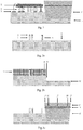
- Step 1 lug bosses on a the silicon substrate 1 are manufactured using a common lithography process and a silicon etching process on the surface of the silicon substrate 1, as seen in Figure 2a .
- the lug bosses comprise a horizontal alignment lug boss 6 and a vertical alignment lug boss 7; i.e., a first silicon etching is performed.
- the etching depth is 10 ⁇ m-100 ⁇ m; that is, the height of the horizontal alignment lug boss 6 and the vertical alignment lug boss 7 formed after etching is 10 ⁇ m-10 ⁇ m.
- the specific etching depth is determined by the height relationship between the silica waveguide layer and the input optical or output optical waveguide on the active optoelectronic chip 5 with respect to the surface of the silicon substrate 1, and the silicon waveguide layer is leveled with the height of the input optical or output optical waveguide on the active optoelectronic chip 5.
- a smooth platform 8 and lug bosses arranged thereon are formed after the first silicon etching, and a first photoresist layer 9 left over by the first silicon etching is reserved above the lug bosses.
- the cross-sectional pattern of the horizontal alignment lug boss 6 and the alignment marks on a waveguide mask, the metal electrode layer 3 and the active optoelectronic chip 5 are identical or complementary, as a reference position for optical coupling and electrical interconnections. If the cross-section of an alignment mark on the active optoelectronic chip 5 is a cross alignment mark, the same cross-sectional pattern of the horizontal alignment lug boss 6 is a cross, and the complementary cross-sectional pattern is with four diamonds for filling the blank in the cross alignment mark.
- the horizontal alignment lug boss 6 is required to be aligned with the alignment mark on the active optoelectronic chip, therefore, the horizontal position thereof is determined by the relative position between the alignment mark on the active optoelectronic chip and the waveguide on the active optoelectronic chip, and the number thereof is determined by the number of alignment marks on the active optoelectronic chip.
- the vertical alignment lug boss 7 is arranged in the middle part of the active optoelectronic chip 5 in a horizontal relative position, is arranged symmetrically on the two sides of the output optical or input optical waveguide on the active optoelectronic chip 5, and could not be connected with any metal electrode layer 3.
- the vertical alignment lug boss 7 is of a structure with a plurality of circular cylinders or square cylinders or the like; the cross-sectional area of a single vertical alignment lug boss 7 is 100 ⁇ m 2 -40000 ⁇ m 2 , the number thereof is 4-10 and the specific number is determined by the ratio between the area of a middle part of the active optoelectronic chip 5 (the substrate area between the direct-current electrode and the alternating-current electrode on the active optoelectronic chip 5) and the cross-sectional area of a single vertical alignment lug boss.
- Step 2 manufacturing a groove 10 on the surface of the platform 8, which is a second silicon etching, as seen in Figure 2b .
- the photoresist 9 left over by the first silicon etching is removed, and a second photoresist layer 11 is manufactured above the platform 8 and the lug bosses using common lithography, the thickness thereof being larger than the height of the lug bosses so as to protect the lug bosses (6, 7) and define the border of the groove 10.
- the groove 10 is then manufactured on the second photoresist layer 11 and one side of the lug boss 8 using the silicon etching process, the etching depth being 100 ⁇ m-1500 ⁇ m and being larger than the thickness of the second photoresist layer 11.
- the second photoresist layer 11 after the second silicon etching is reserved.
- the depth of the groove 10 is 100 ⁇ m-1500 ⁇ m and is specifically determined by the distance from the silica waveguide layer to the bottom surface of the silica element together with the distance from the silica waveguide layer to the surface of the silicon platform 8.
- the groove 10 is a groove of a rectangular shape, the width and length thereof being both larger than the width and length of the silica waveguide element 2, and a side wall in the groove away from the platform 8 in the groove 10 and other two side walls in the groove of the groove next to the side wall are categorized as a reserved area.
- the categorized reserved area is removed in a slicing process after the accomplishment of manufacturing a whole hybrid integrated wafer and thus only a side wall in the groove on the side which is in close proximity to the lug boss 6 and the platform 8 is left over, as shown in Figure 3b .
- Step 3 Manufacturing the silica waveguide element 2 using a silica thermal bonding process.
- Thermal oxidation or plasma enhanced chemical vapor deposition (PECVD) is used on the surface of the groove 10 to grow a silica bonding layer 12, the depth of which being 0.01 ⁇ m-1 ⁇ m, as shown in Figure 2c .
- PECVD plasma enhanced chemical vapor deposition
- the second photoresist layer 11 after the second silicon etching in the step 2 is removed and a prepared silica waveguide element 2 is arranged in the groove 10 on the silicon substrate 1 using again the silica bonding layer 12 through a high-temperature bonding process so that the silica bonding layer 12 is melted into a silica substrate layer 13.
- the structure of a prepared silica waveguide element 2 comprises a silica substrate layer 13, a silica waveguide layer 14 and a silica upper covering layer 15, wherein the silica substrate layer 13 is arranged on the bottom of the groove 10, and the silica waveguide layer 14 is perpendicular to a strip structure on the bottom of the groove 10 and in close proximity to a side wall in the groove.
- the thickness of the silica substrate layer 13 is 500 ⁇ m-1000 ⁇ m
- the thickness of the silica waveguide layer 14 is 3 ⁇ m-50 ⁇ m
- the thickness of the silica upper covering layer 15 is 50 ⁇ m-1000 ⁇ m.
- the silica waveguide layer 14 comprises horizontally the coupling area 16 in close proximity to the active optoelectronic chip, a general waveguide area 17 and an optical fiber coupling area in close proximity to an optical fiber.
- the silica waveguide layer 14 is silica with high refractive index, the difference in refractive index among the silica waveguide layer 14 and the silica substrate layer 13 and the silica upper covering layer 15 is 0.5%-2.5%, and the refractive index of the material of the silica substrate layer 13 is the same as that of the silica upper covering layer 15.
- the waveguide width of the general waveguide area 17 is 6 ⁇ m-9 ⁇ m; the waveguide width of the coupling area in close proximity to the active optoelectronic chip 16 is narrower than that of the general waveguide area 17 and is 3 ⁇ m-7 ⁇ m; and the waveguide width of the coupling area in close proximity to the optical fiber 18 is wider than that of the general waveguide area 17 and is 8 ⁇ m-10 ⁇ m.
- Outside end faces 19 of the coupling area in close proximity to the active optoelectronic chip 16 and the coupling area in close proximity to the optical fiber 18 are both inclined end faces at 5°-45° inclination with respect to the vertical direction, and are perpendicular to the central axis for light output or light input in a vertical waveguide.
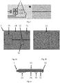
- Step 1 manufacturing the silica waveguide element 2, as shown in Figure 3a .
- a silica substrate layer 13 and a silica waveguide layer 14 grow on the whole silicon substrate 1 using a silica growth process and using plasma enhanced chemical vapor deposition (PECVD).
- PECVD plasma enhanced chemical vapor deposition
- a doped silica waveguide layer 14 can be manufactured using synchronous gas mixture injection, such as germane, etc. for waveguide doping during growth.
- the silica waveguide layer 14 is manufactured using common lithography and silicon etching processes.
- the silica is etched until the silica substrate layer 13 is reached, and the waveguide layer on one side of the light emitting face of the silica waveguide is also etched until the silica substrate layer 13 is reached, the reserved length of the reserved area being 500 ⁇ m-1500 ⁇ m.
- the silica waveguide layer 14 is silica with high refractive index, the difference in refractive index among the silica waveguide layer 14, the silica substrate layer 13 and the silica upper covering layer 15 being 0.5%-2.5%.
- the silica waveguide layer 14 comprises a coupling area in close proximity to the active optoelectronic chip 16, a general waveguide area 17 and a coupling area in close proximity to an optical fiber 18.
- the waveguide width of the general waveguide area 17 is 6 ⁇ m-9 ⁇ m; the waveguide width of the coupling area in close proximity to the active optoelectronic chip 16 is narrower than that of the general waveguide area 17 and is 3 ⁇ m-7 ⁇ m; and the waveguide width of the coupling area in close proximity to the optical fiber 18 is wider than that of the general waveguide area 17 and is 8 ⁇ m-10 ⁇ m.
- the thickness of the silica substrate layer 13 is 50 ⁇ m-1000 ⁇ m, and the thickness of the silica waveguide layer 14 is 3 ⁇ m-50 ⁇ m.
- Step 2 manufacturing the silica upper covering layer and the inclined end faces.
- the silica upper covering layer 15 continues to grow above the silica waveguide layer 14 and the reserved area 20 using the plasma enhanced chemical vapor deposition (PECVD), and then a high-temperature thermal annealing is performed, as shown in Figure 3b .
- PECVD plasma enhanced chemical vapor deposition
- the silica upper covering layer 15 on the upper part of the silica waveguide layer 14 is protected using common lithography, and a part of the upper covering layer 15 is etched off on the reserved area 20 using the silica etching process until the silica substrate layer 13 is exposed, a third photoresist layer 21 left over above the etched silica upper covering layer 15 being reserved, as can be seen in Figure 3c .
- inclined end faces 19 are manufactured on both sides of the silica waveguide layer 14 using an end face polishing process.
- Outside end faces 19 of the coupling area in close proximity to the active optoelectronic chip 16 and the coupling area in close proximity to the optical fiber 18 are both inclined end faces at 5°-45° inclination with respect to the vertical direction, and the outside end faces are perpendicular to the central axis for light output or light input in a vertical waveguide.
- the thickness of the silica covering layer 15 is 50 ⁇ m-1000 ⁇ m.
- Step 3 manufacturing the horizontal alignment lug boss 6 and the vertical alignment lug boss 7.
- the upper covering layer 15 and the waveguide structure on the lower layer thereof are protected and the position and the shape of the silica alignment lug bosses are defined using a fourth photoresist layer 22 on the silica reserved area 20 by using common lithography and silica etching processes.
- the silica substrate layer 13 is etched until the surface of the silicon substrate 1 is reached and a silica vertical alignment lug boss 23 and a silica horizontal alignment lug boss 24 are manufactured, as can be seen in Figure 3d .
- the positions and shapes of the silica horizontal alignment lug boss 24 and the silica vertical alignment lug boss 23 are identical to those of the horizontal alignment lug boss 6 and the vertical alignment lug boss 7 described in step 1, i.e., manufacturing the silica waveguide element using the silica bonding process.
- the fourth photoresist layer 22 left over after etching is reserved and the silica substrate 1 is continuously silicon etched by changing to use the silicon etching process, the etching depth being 10 ⁇ m-100 ⁇ m, as can be seen in Figure 3e .
- the vertical alignment lug boss 7 and a horizontal alignment lug boss 6 are formed on the lower part of the silica vertical alignment lug boss 23 and the silica horizontal alignment lug boss 24.
- the positions and the shape of cross-sections of the silica vertical alignment lug boss 23 and the silica horizontal alignment lug boss 24 manufactured in this method are identical to those of the vertical alignment lug boss 7 and the horizontal alignment lug boss 6, and are identical also to the positions and the shape of cross-sections of the vertical alignment lug boss 7 and the horizontal alignment lug boss 6 described in step 1, i.e., manufacturing the silica waveguide element 2 using the silica bonding process.
- the total height of the silica vertical alignment lug boss 23 and the silica horizontal alignment lug boss 24 and the vertical alignment lug boss 7 and the horizontal alignment lug boss 6 is 10 ⁇ m-100 ⁇ m and the specific height is determined by the relationship in height of the silica waveguide layer 14 and the input optical or output optical waveguide on the active optoelectronic chip 5 with respect to the surface of the silicon substrate 1, and it is guaranteed that the silica waveguide layer 14 is leveled with the height of the input optical or output optical waveguide on the active optoelectronic chip 5. Finally, the third photoresist layer 21 and the fourth photoresist layer 22 left over are removed.
- Step 2 Manufacturing a metal electrode layer 3.
- the silica waveguide area 14 is protected and a metal electrode pattern is defined on the surface of the silicon substrate 1 using the photoresist, the vertical alignment lug boss 7 is used to be aligned with the alignment mark on a metal electrode mask, a metal electrode layer 3 is manufactured on the platform 8 by using common lithography, metal sputtering and steaming, and metal stripping processes, as can be seen in Figures 4a and 4b .
- the thickness of the metal electrode layer 3 is 0.2 ⁇ m-3 ⁇ m and is of a multi-layer structure, such as a Ti/Pt/Au layered structure.
- the metal electrode layer 3 is manufactured on the platform 8 of the silicon substrate 1, and the multi-layer structure of the metal electrode layer 3 is required to be in good contact with the silicon substrate 1 and the solder bumps 4.
- the metal electrode layer 3 is a metal electrode with a special structure and comprises a direct-current electrode area 25, an alternating-current electrode area 26, a ground electrode area 27 and an alignment pattern electrode area 28, the four areas being electrode structures in a horizontal distribution.
- the direct-current electrode area 25 and the alternating-current electrode area 26 are arranged right under the direct-current electrode 29 and the alternating-current electrode 30 of the active optoelectronic chip 5, and solder bumps 4 are manufactured on the direct-current electrode area 25 and the alternating-current electrode area 26 which are used for loading direct-current and alternating-current electrical signals onto the active optoelectronic chip 5.
- Extended electrodes are provided to the direct-current electrode area 25 and the alternating-current electrode area 26 and are extended to the ends away from the lug bosses on the platform 8, so as to facilitate the interconnections with gold wire leads among package tube shells of the chip.
- the ground electrode area 27 is arranged on the end away from the silicon lug bosses on the platform 8 and is connected with the back face electrode of the active optoelectronic chip 5 through gold wire leads. As illustrated before, the alignment pattern electrode area 28 is aligned with the horizontal alignment lug boss 6 in the lug bosses.
- Step 3 the solder bumps 4 are manufactured on the metal electrode layer 3, and an alignment mark 28 of the metal electrode or the silicon horizontal alignment lug boss 6 is aligned with an alignment mark of a ball planting machine for solder bumps, and the solder bumps 4 are manufactured by using ball plant and reflow processes, as can be seen in Figure 5 .
- the solder bumps 4 are only manufactured on the direct-current electrode area 25 and the alternating-current electrode area 26 on the metal electrode layer 3, the number thereof determined by the proportions between the area of the metal electrode and that of the solder bumps 4.
- solder bumps 4 can be manufactured through ball plant and reflow processes, and no solder bumps 4 should overflow the direct-current electrode area 25 and the alternating-current electrode area 26 of the metal electrode layer 3 during the ball plant and reflow procedure and in the later bonding process for the active optoelectronic chip 5.
- Step 4 soldering the active optoelectronic chip 5.
- the active optoelectronic chip 5 is a waveguide-type III-V laser or detector, the frontal surface thereof being provided with a direct-current electrode 29, an alternating-current electrode 30 and an alignment mark 31, the middle part thereof being provided with an output optical or input optical waveguide 32, and the back face thereof being provided with a ground electrode 33, the lower part of the electrode on the frontal surface being the front surface 34, as can be seen in Figure 6a- Figure 6c .
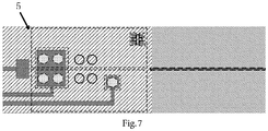
- the alignment pattern electrode area 28 or the horizontal alignment lug boss 6 are used to be aligned with the alignment mark 31 on the active optoelectronic chip 5, and the metal electrode layer 3 of the active optoelectronic chip 5 is manufactured on the solder bumps 4 by using the combined processes of thermal reflow soldering and flip-chip bonding, as can be seen in Figure 7 .
- the direct-current electrode 29 and the alternating-current electrode 30 on the frontal surface contact with the upper part of the solder bumps 4 in the direct-current electrode area 25 and the alternating-current electrode area 26 on the metal electrode layer 3, respectively. After the contact with the solder bumps 4, the alignment mark on the frontal surface is aligned with the alignment mark of the alignment pattern electrode area 28 or the horizontal alignment lug boss 6.
- An alloy is formed between the direct-current electrode 29 and alternating-current electrode 30 on the frontal surface on the active optoelectronic chip 5 and the solder bumps 4 using the combined processes of thermal reflow soldering and flip chip bonding, and the chip is pressed down until the frontal surface 34 of the active optoelectronic chip 5 contacts with the silicon vertical alignment lug boss 7, as can be seen in Figure 1 .
- Step 5 the ground electrode 33 on the back surface of the active optoelectronic chip 5 is connected with the ground electrode area 27 on the metal electrode layer 3 through a gold wire, as shown in Figure 1 .
Landscapes
- Physics & Mathematics (AREA)
- General Physics & Mathematics (AREA)
- Optics & Photonics (AREA)
- Engineering & Computer Science (AREA)
- Microelectronics & Electronic Packaging (AREA)
- Optical Couplings Of Light Guides (AREA)
- Optical Integrated Circuits (AREA)
- Manufacturing & Machinery (AREA)
Claims (7)
- Integrierter optoelektronischer Hybrid-Chip auf Siliziumdioxid-auf-Silizium-Basis, der ein Siliziumsubstrat (1) umfasst, wobei die Oberfläche des Siliziumsubstrats mit einer Plattform (8) und einer Rinne (10) versehen ist, wobei ein Siliziumdioxid-Wellenleiterelement (2) in der Rinne angeordnet ist, dadurch gekennzeichnet, dass die Oberfläche des Siliziumsubstrats ferner mit Ösenvorsprüngen (6, 7) versehen ist, die aus einer Oberfläche der Plattform vorstehen, die Oberfläche der Plattform mit einer unterbrochenen Metallelektrodenschicht (3) versehen ist, die Oberfläche der Metallelektrodenschicht mit Lötperlen (4) versehen ist und ein aktiver optoelektronischer Chip (5) über den Lötperlen und den Ösenvorsprüngen angeordnet ist, wobei die vorstehenden Ösenvorsprünge (6, 7) einen horizontalen Ausrichtungsösenvorsprung (6) und einen vertikalen Ausrichtungsösenvorsprung (7) umfassen, wobei die Höhe des horizontalen Ausrichtungsösenvorsprungs gleich der des vertikalen Ausrichtungsösenvorsprungs ist, von denen beide 10 µm-100 µm betragen.
- Integrierter optoelektronischer Hybrid-Chip auf Siliziumdioxid-auf-Silizium-Basis nach Anspruch 1, dadurch gekennzeichnet, dass das Siliziumdioxid-Wellenleiterelement (2) in Längsrichtung aufeinanderfolgend eine Siliziumdioxid-Substratschicht (13), eine Siliziumdioxid-Wellenleiterschicht (14) und eine obere Siliziumdioxid-Deckschicht (15) umfasst; das Siliziumdioxid-Wellenleiterelement horizontal aufeinanderfolgend einen Wellenleiterbereich (17), einen Kopplungsbereich (16) in unmittelbarer Nähe zum aktiven optoelektronischen Chip und einen Kopplungsbereich (18) in unmittelbarer Nähe zu einem Lichtwellenleiter umfasst; die Breite des Wellenleiters im Kopplungsbereich in unmittelbarer Nähe zum aktiven optoelektronischen Chip 3 µm-7 µm beträgt; und die Breite des Wellenleiters im Kopplungsbereich in unmittelbarer Nähe zum Lichtwellenleiter 6 µm-10 µm beträgt.
- Integrierter optoelektronischer Hybrid-Chip auf Siliziumdioxid-auf-Silizium-Basis nach Anspruch 2, dadurch gekennzeichnet, dass die Anzahl und die horizontale Position des horizontalen Ausrichtungsösenvorsprungs (6, 24) durch die relative Position einer Ausrichtungsmarkierung (31) auf dem aktiven optoelektronischen Chip (5) und eines Wellenleiters auf dem aktiven optoelektronischen Chip (5) bestimmt werden, die Höhe des vertikalen Ausrichtungsösenvorsprungs (7, 23) durch die vertikale Position der Siliziumdioxid-Wellenleiterschicht (14) im Siliziumdioxid-Wellenleiterelement (2) bestimmt wird und der vertikale Ausrichtungsösenvorsprung an einem Mittelteil des aktiven optoelektronischen Chips angeordnet ist.
- Integrierter optoelektronischer Hybrid-Chip auf Siliziumdioxid-auf-Silizium-Basis nach Anspruch 1, dadurch gekennzeichnet, dass die Dicke der Metallelektrodenschicht (3) 0,2 µm-3 µm beträgt und die Metallelektrodenschicht einen Gleichstromelektrodenbereich (25), einen Wechselstromelektrodenbereich (26), einen Erdungselektrodenbereich (27) und einen Ausrichtungsmuster-Elektrodenbereich (28) umfasst; die Ösenvorsprünge zwischen dem Gleichstromelektrodenbereich und dem Wechselstromelektrodenbereich angeordnet sind und der Gleichstromelektrodenbereich und der Wechselstromelektrodenbereich, über denen die Lötperlen (4) gefertigt sind, eine Gleichstromelektrode und die Wechselstromelektrode des aktiven optoelektronischen Chips (5) über die Lötperlen kontaktieren; eine vordere Ausrichtungsmarkierung des aktiven optoelektronischen Chips und der horizontale Ausrichtungsösenvorsprung oder die Ausrichtungsmarkierung der Metallelektrodenschicht ausgerichtet sind; und eine rückseitige Elektrode (33) des aktiven optoelektronischen Chips mit dem Erdungselektrodenbereich der Metallelektrodenschicht verbunden ist.
- Integrierter optoelektronischer Hybrid-Chip auf Siliziumdioxid-auf-Silizium-Basis nach Anspruch 1, dadurch gekennzeichnet, dass das Siliziumdioxid-Wellenleiterelement (2) mit einer äußeren Endfläche mit einer 5°-45°-Neigung zur vertikalen Richtung versehen ist.
- Herstellungsverfahren für einen integrierten optoelektronischen Hybrid-Chip auf Siliziumdioxid-auf-Silizium-Basis, das die folgenden Schritte umfasst:Herstellen eines Siliziumsubstrats (1);Herstellen eines horizontalen Ausrichtungsösenvorsprungs (6) und eines vertikalen Ausrichtungsösenvorsprungs (7) auf einer Oberfläche des Siliziumsubstrats (1), wobei die Höhe des horizontalen Ausrichtungsösenvorsprungs gleich der des vertikalen Ausrichtungsösenvorsprungs ist, von denen beide 10 µm-100 µm betragen;Herstellen einer Rinne (10) auf einer Seite der Ösenvorsprünge auf dem Siliziumsubstrat;Anordnen eines Siliziumdioxid-Wellenleiterelements (2) in der Rinne (10) des Siliziumsubstrats unter Verwendung eines thermalen Siliziumdioxid-Bindungsprozesses;Herstellen einer unterbrochenen Metallelektrodenschicht (3) auf dem Siliziumsubstrat;Herstellen von Lötperlen (4) über einem Gleichstromelektrodenbereich (25) und einem Wechselstromelektrodenbereich (26) der Metallelektrodenschicht;Löten eines aktiven optoelektronischen Chips (5) über den Lötperlen, dem vertikalen Ausrichtungsösenvorsprung (7) und dem horizontalen Ausrichtungsösenvorsprung (6).
- Herstellungsverfahren für einen integrierten optoelektronischen Hybrid-Chip auf Siliziumdioxid-auf-Silizium-Basis nach Anspruch 6, das ferner die Schritte umfasst zum:
Aufwachsen einer Siliziumdioxid-Bindungsschicht (12) auf den Boden der Rinne, Einsetzen des Siliziumdioxid-Wellenleiterelements (2) in die Rinnenstruktur unter Verwendung eines thermalen Siliziumdioxid-Bindungsprozesses, sodass die Bindungsschicht in eine Siliziumdioxid-Substratschicht (13) des Siliziumdioxid-Wellenleiterelements eingeschmolzen wird, und Versehen des Siliziumdioxid-Wellenleiterelements mit einer äußeren Endfläche mit einer 5°-45°-Neigung zur vertikalen Richtung.
Applications Claiming Priority (2)
| Application Number | Priority Date | Filing Date | Title |
|---|---|---|---|
| CN201210586072.XA CN103066148B (zh) | 2012-12-28 | 2012-12-28 | 一种硅上二氧化硅基的混合集成光电子芯片及其制作方法 |
| PCT/CN2013/090492 WO2014101780A1 (zh) | 2012-12-28 | 2013-12-26 | 一种硅上二氧化硅基的混合集成光电子芯片及其制作方法 |
Publications (3)
| Publication Number | Publication Date |
|---|---|
| EP2940739A1 EP2940739A1 (de) | 2015-11-04 |
| EP2940739A4 EP2940739A4 (de) | 2016-01-13 |
| EP2940739B1 true EP2940739B1 (de) | 2019-06-12 |
Family
ID=48108693
Family Applications (1)
| Application Number | Title | Priority Date | Filing Date |
|---|---|---|---|
| EP13867481.7A Active EP2940739B1 (de) | 2012-12-28 | 2013-12-26 | Hybrider, integrierter optoelektronischer silica-auf-silicium-chip und herstellungsverfahren dafür |
Country Status (4)
| Country | Link |
|---|---|
| US (1) | US9482831B2 (de) |
| EP (1) | EP2940739B1 (de) |
| CN (1) | CN103066148B (de) |
| WO (1) | WO2014101780A1 (de) |
Families Citing this family (35)
| Publication number | Priority date | Publication date | Assignee | Title |
|---|---|---|---|---|
| CN103066148B (zh) * | 2012-12-28 | 2015-05-20 | 武汉电信器件有限公司 | 一种硅上二氧化硅基的混合集成光电子芯片及其制作方法 |
| CN105445854B (zh) | 2015-11-06 | 2018-09-25 | 南京邮电大学 | 硅衬底悬空led光波导集成光子器件及其制备方法 |
| CN105717586B (zh) * | 2016-03-31 | 2017-09-01 | 武汉光迅科技股份有限公司 | 一种sip芯片与激光器的耦合方法及其组成的光收发模块 |
| CN105866903B (zh) * | 2016-05-18 | 2019-01-22 | 武汉光迅科技股份有限公司 | 一种激光器与平面光波导混合集成结构及其制造方法 |
| US9857532B2 (en) * | 2016-05-19 | 2018-01-02 | Advanced Semiconductor Engineering, Inc. | Semiconductor device packages |
| CN106449479A (zh) * | 2016-09-30 | 2017-02-22 | 山东盛品电子技术有限公司 | 用于芯片区域裸露封装的单元封装体模具及精准成型模具 |
| CN108873182B (zh) * | 2017-05-12 | 2020-01-03 | 华为技术有限公司 | 光开关芯片 |
| JP2019028116A (ja) * | 2017-07-26 | 2019-02-21 | 住友ベークライト株式会社 | 光導波路、光導波路接続体および電子機器 |
| CN107516684A (zh) * | 2017-08-25 | 2017-12-26 | 深圳市芯思杰智慧传感技术有限公司 | 光电二极管芯片及其制作方法 |
| CN109713563A (zh) * | 2017-10-26 | 2019-05-03 | 上海矽安光电科技有限公司 | 一种半导体激光器无源对准耦合与高频封装用硅基板 |
| CN108054182B (zh) * | 2017-12-19 | 2024-04-12 | 苏州矩阵光电有限公司 | 一种化合物半导体硅基混合器件及其制备方法 |
| CN109143466B (zh) * | 2018-08-31 | 2020-04-14 | 武汉光迅科技股份有限公司 | 一种混合集成硅光芯片、光器件及芯片制作方法 |
| EP3674759A1 (de) * | 2018-12-31 | 2020-07-01 | Indigo Diabetes N.V. | Integration einer aktiven komponente auf einer photonikplattform |
| CN111856654B (zh) * | 2019-04-11 | 2022-11-18 | 联合微电子中心有限责任公司 | 一种激光器芯片与硅基光电子芯片的耦合对准方法及装置 |
| CN109917353B (zh) * | 2019-04-23 | 2020-05-19 | 上海禾赛光电科技有限公司 | 激光雷达的激光发射装置以及激光雷达 |
| CN110361819B (zh) * | 2019-07-26 | 2020-10-30 | 中国科学院半导体研究所 | 有源芯片与无源光波导芯片的三维对准方法及结构 |
| US11169328B2 (en) * | 2019-09-20 | 2021-11-09 | Taiwan Semiconductor Manufacturing Co., Ltd. | Photonic structure and method for forming the same |
| CN113555449B (zh) * | 2020-04-03 | 2024-03-15 | 华为技术有限公司 | 半导体器件及其制备方法和通信设备 |
| WO2022123598A1 (en) * | 2020-12-10 | 2022-06-16 | Lightspeedai Labs Private Limited | Systems and methods for enabling an optics based compute system associated with transmission and reception |
| CN113156592A (zh) * | 2020-12-31 | 2021-07-23 | 武汉联特科技股份有限公司 | 光发射coc组件以及光发射器件 |
| CN113161450B (zh) * | 2021-04-25 | 2022-11-25 | 中国科学院长春光学精密机械与物理研究所 | 一种集成光信号计算装置的制备方法 |
| CN115453779A (zh) * | 2021-06-08 | 2022-12-09 | 武汉光迅科技股份有限公司 | 光波导器件及其制作方法 |
| US20250155657A1 (en) * | 2022-02-22 | 2025-05-15 | Kyocera Corporation | Optical circuit board |
| CN117897647A (zh) * | 2022-03-07 | 2024-04-16 | 麦斯卓微电子(南京)有限公司 | Mems透镜/图像传感器组件和工艺流程 |
| WO2023211900A1 (en) * | 2022-04-26 | 2023-11-02 | Aayuna Inc. | Passive alignment configuration for use with optical waveguides formed within adjoining substrates |
| CN115657226B (zh) * | 2022-10-26 | 2023-06-23 | 之江实验室 | 一种硅基光交换芯片的光电扇出结构及其制备方法 |
| CN115421247A (zh) * | 2022-11-07 | 2022-12-02 | 北京浦丹光电股份有限公司 | 一种光耦合结构 |
| CN115877521B (zh) * | 2022-11-28 | 2026-03-13 | 之江实验室 | 堆叠封装结构和堆叠封装结构的制作方法 |
| CN116466552A (zh) * | 2023-04-28 | 2023-07-21 | 无锡兴华衡辉科技有限公司 | 对位标记及其应用、读出电路芯片及其应用 |
| US20250044534A1 (en) * | 2023-07-31 | 2025-02-06 | Ayar Labs, Inc. | Direct Silicon-to-Silicon Bonding for Fiber-First Packaging Process |
| CN117310901A (zh) * | 2023-09-22 | 2023-12-29 | 无锡芯光互连技术研究院有限公司 | 单行载流子光电二极管片上集成结构及方法 |
| US20250102751A1 (en) * | 2023-09-25 | 2025-03-27 | Ciena Corporation | Managing co-packaging of photonic integrated circuits |
| CN117406350A (zh) * | 2023-10-27 | 2024-01-16 | 武汉光谷信息光电子创新中心有限公司 | 一种倒装键合的激光器与硅光波导耦合结构及方法 |
| CN120255070A (zh) * | 2024-01-02 | 2025-07-04 | 武汉光迅科技股份有限公司 | 一种玻璃与硅光的混合集成结构及其制作方法 |
| WO2026015727A1 (en) * | 2024-07-10 | 2026-01-15 | Government Of The United States Of America, As Represented By The Secretary Of Commerce | Photonic article and making a photonic article |
Family Cites Families (13)
| Publication number | Priority date | Publication date | Assignee | Title |
|---|---|---|---|---|
| EP0617303A1 (de) * | 1993-03-19 | 1994-09-28 | Akzo Nobel N.V. | Ein Verfahren zur Integration eines Halbleiterbauelements mit einem polymerenoptischen Wellenleiter-Bauelement, und eine elektro-optische Vorrichtung mit einer so herstellbaren integrierten Struktur |
| KR100283075B1 (ko) * | 1998-11-05 | 2001-03-02 | 이계철 | 수동정렬법을 이용한 광소자-플라나 광파회로-광섬유의 광축 정렬방법 |
| US7110169B1 (en) * | 2000-12-14 | 2006-09-19 | Finisar Corporation | Integrated optical device including a vertical lasing semiconductor optical amplifier |
| JP4779255B2 (ja) * | 2001-07-16 | 2011-09-28 | パナソニック株式会社 | レーザ光源 |
| KR20050070263A (ko) * | 2003-12-30 | 2005-07-07 | 마이크로솔루션스 주식회사 | 복합형 광소자, 복합형 광소자용 실리콘 광학 벤치,복합형 광소자용 평면형 광도파로 소자, 복합형 광소자의제조방법, 및 이를 위한 광소자의 광축 정렬 방법 |
| US7369718B2 (en) * | 2004-01-23 | 2008-05-06 | Intel Corporation | Package substrate pattern to accommodate optical waveguide |
| US8116624B1 (en) * | 2007-01-29 | 2012-02-14 | Cirrex Systems Llc | Method and system for evaluating an optical device |
| JP5186785B2 (ja) * | 2007-03-23 | 2013-04-24 | 日本電気株式会社 | 光導波路デバイス、光導波路デバイス用光素子実装システム、光素子実装方法、及びそのプログラム |
| US7978742B1 (en) * | 2010-03-24 | 2011-07-12 | Corning Incorporated | Methods for operating diode lasers |
| CN102005497A (zh) * | 2009-09-02 | 2011-04-06 | 中国科学院半导体研究所 | 用于片上光互连的接收模块封装方法 |
| CN102053318A (zh) * | 2009-11-04 | 2011-05-11 | 中国科学院半导体研究所 | 在硅平台上实现awg与ld倒装集成的方法 |
| US9151664B2 (en) * | 2012-08-03 | 2015-10-06 | Hoya Corporation Usa | Submount for optoelectronic, optical, or photonic components |
| CN103066148B (zh) * | 2012-12-28 | 2015-05-20 | 武汉电信器件有限公司 | 一种硅上二氧化硅基的混合集成光电子芯片及其制作方法 |
-
2012
- 2012-12-28 CN CN201210586072.XA patent/CN103066148B/zh active Active
-
2013
- 2013-12-26 WO PCT/CN2013/090492 patent/WO2014101780A1/zh not_active Ceased
- 2013-12-26 EP EP13867481.7A patent/EP2940739B1/de active Active
- 2013-12-26 US US14/758,416 patent/US9482831B2/en active Active
Non-Patent Citations (1)
| Title |
|---|
| None * |
Also Published As
| Publication number | Publication date |
|---|---|
| US9482831B2 (en) | 2016-11-01 |
| US20150355424A1 (en) | 2015-12-10 |
| CN103066148B (zh) | 2015-05-20 |
| WO2014101780A1 (zh) | 2014-07-03 |
| EP2940739A4 (de) | 2016-01-13 |
| EP2940739A1 (de) | 2015-11-04 |
| CN103066148A (zh) | 2013-04-24 |
Similar Documents
| Publication | Publication Date | Title |
|---|---|---|
| EP2940739B1 (de) | Hybrider, integrierter optoelektronischer silica-auf-silicium-chip und herstellungsverfahren dafür | |
| TWI648563B (zh) | 積體模組及其形成方法 | |
| US7522648B2 (en) | Hybrid type integrated optical device | |
| US11340400B2 (en) | Hybrid integration for photonic integrated circuits | |
| KR102355831B1 (ko) | 자가-테스트 기능성을 가진 수직 입사 광검출기 | |
| US12222566B2 (en) | Self-aligned structure and method on interposer-based PIC | |
| Moscoso-Mártir et al. | Hybrid silicon photonics flip-chip laser integration with vertical self-alignment | |
| JP2020521186A (ja) | 光相互接続装置及び光相互接続装置の作製方法 | |
| CN109143466B (zh) | 一种混合集成硅光芯片、光器件及芯片制作方法 | |
| CN105866903A (zh) | 一种激光器与平面光波导混合集成结构及其制造方法 | |
| CN110192136A (zh) | 光学中介层光电装置 | |
| CN104538480A (zh) | 高速InGaAs光电探测器芯片倒装集成结构及制作方法 | |
| CN103022893B (zh) | 一种用于电吸收调制激光器与硅基波导集成的高频电极 | |
| WO2019061897A1 (zh) | 一种多通道高速率光模块结构和加工方法 | |
| TWI848611B (zh) | 光學裝置與其製造方法 | |
| CN217981913U (zh) | 一种混合集成器件 | |
| US20140029890A1 (en) | Optical system with integrated photodetectors | |
| Kapulainen et al. | Hybrid integration of InP lasers with SOI waveguides using thermocompression bonding | |
| CN221746334U (zh) | 一种多阵列异质集成密集波分复用光电器件 | |
| TWI870066B (zh) | 積體電路裝置的製造方法及光學裝置 | |
| US20260050130A1 (en) | Improved Light Source Integration | |
| US20250133865A1 (en) | Solder bridge metallization using solder ball jetting | |
| CN221746335U (zh) | 一种多阵列异质集成密集波分复用可调谐光电器件 | |
| US20230021029A1 (en) | Wafer-level optoelectronic packaging | |
| Li et al. | Photolithography of 3D topology in Si optical bench for self-aligned placement of laser dies |
Legal Events
| Date | Code | Title | Description |
|---|---|---|---|
| PUAI | Public reference made under article 153(3) epc to a published international application that has entered the european phase |
Free format text: ORIGINAL CODE: 0009012 |
|
| 17P | Request for examination filed |
Effective date: 20150708 |
|
| AK | Designated contracting states |
Kind code of ref document: A1 Designated state(s): AL AT BE BG CH CY CZ DE DK EE ES FI FR GB GR HR HU IE IS IT LI LT LU LV MC MK MT NL NO PL PT RO RS SE SI SK SM TR |
|
| AX | Request for extension of the european patent |
Extension state: BA ME |
|
| A4 | Supplementary search report drawn up and despatched |
Effective date: 20151211 |
|
| RIC1 | Information provided on ipc code assigned before grant |
Ipc: G02B 6/42 20060101ALI20151207BHEP Ipc: H01L 31/18 20060101ALI20151207BHEP Ipc: H01L 31/12 20060101AFI20151207BHEP |
|
| DAX | Request for extension of the european patent (deleted) | ||
| STAA | Information on the status of an ep patent application or granted ep patent |
Free format text: STATUS: EXAMINATION IS IN PROGRESS |
|
| 17Q | First examination report despatched |
Effective date: 20180323 |
|
| REG | Reference to a national code |
Ref country code: DE Ref legal event code: R079 Ref document number: 602013056659 Country of ref document: DE Free format text: PREVIOUS MAIN CLASS: H01L0031120000 Ipc: G02B0006420000 |
|
| RIC1 | Information provided on ipc code assigned before grant |
Ipc: G02B 6/42 20060101AFI20181127BHEP Ipc: H01L 31/0232 20140101ALI20181127BHEP Ipc: H01L 31/18 20060101ALN20181127BHEP |
|
| GRAP | Despatch of communication of intention to grant a patent |
Free format text: ORIGINAL CODE: EPIDOSNIGR1 |
|
| STAA | Information on the status of an ep patent application or granted ep patent |
Free format text: STATUS: GRANT OF PATENT IS INTENDED |
|
| INTG | Intention to grant announced |
Effective date: 20190110 |
|
| GRAS | Grant fee paid |
Free format text: ORIGINAL CODE: EPIDOSNIGR3 |
|
| GRAA | (expected) grant |
Free format text: ORIGINAL CODE: 0009210 |
|
| STAA | Information on the status of an ep patent application or granted ep patent |
Free format text: STATUS: THE PATENT HAS BEEN GRANTED |
|
| AK | Designated contracting states |
Kind code of ref document: B1 Designated state(s): AL AT BE BG CH CY CZ DE DK EE ES FI FR GB GR HR HU IE IS IT LI LT LU LV MC MK MT NL NO PL PT RO RS SE SI SK SM TR |
|
| REG | Reference to a national code |
Ref country code: GB Ref legal event code: FG4D |
|
| REG | Reference to a national code |
Ref country code: CH Ref legal event code: EP |
|
| REG | Reference to a national code |
Ref country code: AT Ref legal event code: REF Ref document number: 1143313 Country of ref document: AT Kind code of ref document: T Effective date: 20190615 |
|
| REG | Reference to a national code |
Ref country code: DE Ref legal event code: R096 Ref document number: 602013056659 Country of ref document: DE |
|
| REG | Reference to a national code |
Ref country code: IE Ref legal event code: FG4D |
|
| REG | Reference to a national code |
Ref country code: NL Ref legal event code: MP Effective date: 20190612 |
|
| REG | Reference to a national code |
Ref country code: LT Ref legal event code: MG4D |
|
| PG25 | Lapsed in a contracting state [announced via postgrant information from national office to epo] |
Ref country code: FI Free format text: LAPSE BECAUSE OF FAILURE TO SUBMIT A TRANSLATION OF THE DESCRIPTION OR TO PAY THE FEE WITHIN THE PRESCRIBED TIME-LIMIT Effective date: 20190612 Ref country code: NO Free format text: LAPSE BECAUSE OF FAILURE TO SUBMIT A TRANSLATION OF THE DESCRIPTION OR TO PAY THE FEE WITHIN THE PRESCRIBED TIME-LIMIT Effective date: 20190912 Ref country code: LT Free format text: LAPSE BECAUSE OF FAILURE TO SUBMIT A TRANSLATION OF THE DESCRIPTION OR TO PAY THE FEE WITHIN THE PRESCRIBED TIME-LIMIT Effective date: 20190612 Ref country code: HR Free format text: LAPSE BECAUSE OF FAILURE TO SUBMIT A TRANSLATION OF THE DESCRIPTION OR TO PAY THE FEE WITHIN THE PRESCRIBED TIME-LIMIT Effective date: 20190612 Ref country code: SE Free format text: LAPSE BECAUSE OF FAILURE TO SUBMIT A TRANSLATION OF THE DESCRIPTION OR TO PAY THE FEE WITHIN THE PRESCRIBED TIME-LIMIT Effective date: 20190612 Ref country code: AL Free format text: LAPSE BECAUSE OF FAILURE TO SUBMIT A TRANSLATION OF THE DESCRIPTION OR TO PAY THE FEE WITHIN THE PRESCRIBED TIME-LIMIT Effective date: 20190612 |
|
| PG25 | Lapsed in a contracting state [announced via postgrant information from national office to epo] |
Ref country code: GR Free format text: LAPSE BECAUSE OF FAILURE TO SUBMIT A TRANSLATION OF THE DESCRIPTION OR TO PAY THE FEE WITHIN THE PRESCRIBED TIME-LIMIT Effective date: 20190913 Ref country code: LV Free format text: LAPSE BECAUSE OF FAILURE TO SUBMIT A TRANSLATION OF THE DESCRIPTION OR TO PAY THE FEE WITHIN THE PRESCRIBED TIME-LIMIT Effective date: 20190612 Ref country code: RS Free format text: LAPSE BECAUSE OF FAILURE TO SUBMIT A TRANSLATION OF THE DESCRIPTION OR TO PAY THE FEE WITHIN THE PRESCRIBED TIME-LIMIT Effective date: 20190612 Ref country code: BG Free format text: LAPSE BECAUSE OF FAILURE TO SUBMIT A TRANSLATION OF THE DESCRIPTION OR TO PAY THE FEE WITHIN THE PRESCRIBED TIME-LIMIT Effective date: 20190912 |
|
| REG | Reference to a national code |
Ref country code: AT Ref legal event code: MK05 Ref document number: 1143313 Country of ref document: AT Kind code of ref document: T Effective date: 20190612 |
|
| PG25 | Lapsed in a contracting state [announced via postgrant information from national office to epo] |
Ref country code: SK Free format text: LAPSE BECAUSE OF FAILURE TO SUBMIT A TRANSLATION OF THE DESCRIPTION OR TO PAY THE FEE WITHIN THE PRESCRIBED TIME-LIMIT Effective date: 20190612 Ref country code: RO Free format text: LAPSE BECAUSE OF FAILURE TO SUBMIT A TRANSLATION OF THE DESCRIPTION OR TO PAY THE FEE WITHIN THE PRESCRIBED TIME-LIMIT Effective date: 20190612 Ref country code: CZ Free format text: LAPSE BECAUSE OF FAILURE TO SUBMIT A TRANSLATION OF THE DESCRIPTION OR TO PAY THE FEE WITHIN THE PRESCRIBED TIME-LIMIT Effective date: 20190612 Ref country code: PT Free format text: LAPSE BECAUSE OF FAILURE TO SUBMIT A TRANSLATION OF THE DESCRIPTION OR TO PAY THE FEE WITHIN THE PRESCRIBED TIME-LIMIT Effective date: 20191014 Ref country code: AT Free format text: LAPSE BECAUSE OF FAILURE TO SUBMIT A TRANSLATION OF THE DESCRIPTION OR TO PAY THE FEE WITHIN THE PRESCRIBED TIME-LIMIT Effective date: 20190612 Ref country code: NL Free format text: LAPSE BECAUSE OF FAILURE TO SUBMIT A TRANSLATION OF THE DESCRIPTION OR TO PAY THE FEE WITHIN THE PRESCRIBED TIME-LIMIT Effective date: 20190612 Ref country code: EE Free format text: LAPSE BECAUSE OF FAILURE TO SUBMIT A TRANSLATION OF THE DESCRIPTION OR TO PAY THE FEE WITHIN THE PRESCRIBED TIME-LIMIT Effective date: 20190612 |
|
| PG25 | Lapsed in a contracting state [announced via postgrant information from national office to epo] |
Ref country code: IT Free format text: LAPSE BECAUSE OF FAILURE TO SUBMIT A TRANSLATION OF THE DESCRIPTION OR TO PAY THE FEE WITHIN THE PRESCRIBED TIME-LIMIT Effective date: 20190612 Ref country code: ES Free format text: LAPSE BECAUSE OF FAILURE TO SUBMIT A TRANSLATION OF THE DESCRIPTION OR TO PAY THE FEE WITHIN THE PRESCRIBED TIME-LIMIT Effective date: 20190612 Ref country code: SM Free format text: LAPSE BECAUSE OF FAILURE TO SUBMIT A TRANSLATION OF THE DESCRIPTION OR TO PAY THE FEE WITHIN THE PRESCRIBED TIME-LIMIT Effective date: 20190612 Ref country code: IS Free format text: LAPSE BECAUSE OF FAILURE TO SUBMIT A TRANSLATION OF THE DESCRIPTION OR TO PAY THE FEE WITHIN THE PRESCRIBED TIME-LIMIT Effective date: 20191012 |
|
| REG | Reference to a national code |
Ref country code: DE Ref legal event code: R097 Ref document number: 602013056659 Country of ref document: DE |
|
| PG25 | Lapsed in a contracting state [announced via postgrant information from national office to epo] |
Ref country code: TR Free format text: LAPSE BECAUSE OF FAILURE TO SUBMIT A TRANSLATION OF THE DESCRIPTION OR TO PAY THE FEE WITHIN THE PRESCRIBED TIME-LIMIT Effective date: 20190612 |
|
| PLBE | No opposition filed within time limit |
Free format text: ORIGINAL CODE: 0009261 |
|
| STAA | Information on the status of an ep patent application or granted ep patent |
Free format text: STATUS: NO OPPOSITION FILED WITHIN TIME LIMIT |
|
| PG25 | Lapsed in a contracting state [announced via postgrant information from national office to epo] |
Ref country code: PL Free format text: LAPSE BECAUSE OF FAILURE TO SUBMIT A TRANSLATION OF THE DESCRIPTION OR TO PAY THE FEE WITHIN THE PRESCRIBED TIME-LIMIT Effective date: 20190612 Ref country code: DK Free format text: LAPSE BECAUSE OF FAILURE TO SUBMIT A TRANSLATION OF THE DESCRIPTION OR TO PAY THE FEE WITHIN THE PRESCRIBED TIME-LIMIT Effective date: 20190612 |
|
| 26N | No opposition filed |
Effective date: 20200313 |
|
| PG25 | Lapsed in a contracting state [announced via postgrant information from national office to epo] |
Ref country code: IS Free format text: LAPSE BECAUSE OF FAILURE TO SUBMIT A TRANSLATION OF THE DESCRIPTION OR TO PAY THE FEE WITHIN THE PRESCRIBED TIME-LIMIT Effective date: 20200224 Ref country code: SI Free format text: LAPSE BECAUSE OF FAILURE TO SUBMIT A TRANSLATION OF THE DESCRIPTION OR TO PAY THE FEE WITHIN THE PRESCRIBED TIME-LIMIT Effective date: 20190612 |
|
| PG2D | Information on lapse in contracting state deleted |
Ref country code: IS |
|
| REG | Reference to a national code |
Ref country code: CH Ref legal event code: PL |
|
| REG | Reference to a national code |
Ref country code: BE Ref legal event code: MM Effective date: 20191231 |
|
| PG25 | Lapsed in a contracting state [announced via postgrant information from national office to epo] |
Ref country code: MC Free format text: LAPSE BECAUSE OF FAILURE TO SUBMIT A TRANSLATION OF THE DESCRIPTION OR TO PAY THE FEE WITHIN THE PRESCRIBED TIME-LIMIT Effective date: 20190612 |
|
| PG25 | Lapsed in a contracting state [announced via postgrant information from national office to epo] |
Ref country code: IE Free format text: LAPSE BECAUSE OF NON-PAYMENT OF DUE FEES Effective date: 20191226 Ref country code: LU Free format text: LAPSE BECAUSE OF NON-PAYMENT OF DUE FEES Effective date: 20191226 |
|
| PG25 | Lapsed in a contracting state [announced via postgrant information from national office to epo] |
Ref country code: LI Free format text: LAPSE BECAUSE OF NON-PAYMENT OF DUE FEES Effective date: 20191231 Ref country code: BE Free format text: LAPSE BECAUSE OF NON-PAYMENT OF DUE FEES Effective date: 20191231 Ref country code: CH Free format text: LAPSE BECAUSE OF NON-PAYMENT OF DUE FEES Effective date: 20191231 |
|
| PG25 | Lapsed in a contracting state [announced via postgrant information from national office to epo] |
Ref country code: CY Free format text: LAPSE BECAUSE OF FAILURE TO SUBMIT A TRANSLATION OF THE DESCRIPTION OR TO PAY THE FEE WITHIN THE PRESCRIBED TIME-LIMIT Effective date: 20190612 |
|
| PG25 | Lapsed in a contracting state [announced via postgrant information from national office to epo] |
Ref country code: MT Free format text: LAPSE BECAUSE OF FAILURE TO SUBMIT A TRANSLATION OF THE DESCRIPTION OR TO PAY THE FEE WITHIN THE PRESCRIBED TIME-LIMIT Effective date: 20190612 Ref country code: HU Free format text: LAPSE BECAUSE OF FAILURE TO SUBMIT A TRANSLATION OF THE DESCRIPTION OR TO PAY THE FEE WITHIN THE PRESCRIBED TIME-LIMIT; INVALID AB INITIO Effective date: 20131226 |
|
| PG25 | Lapsed in a contracting state [announced via postgrant information from national office to epo] |
Ref country code: MK Free format text: LAPSE BECAUSE OF FAILURE TO SUBMIT A TRANSLATION OF THE DESCRIPTION OR TO PAY THE FEE WITHIN THE PRESCRIBED TIME-LIMIT Effective date: 20190612 |
|
| PGFP | Annual fee paid to national office [announced via postgrant information from national office to epo] |
Ref country code: DE Payment date: 20251021 Year of fee payment: 13 |
|
| PGFP | Annual fee paid to national office [announced via postgrant information from national office to epo] |
Ref country code: GB Payment date: 20251105 Year of fee payment: 13 |
|
| PGFP | Annual fee paid to national office [announced via postgrant information from national office to epo] |
Ref country code: FR Payment date: 20251105 Year of fee payment: 13 |