EP2933831A1 - Verfahren zur herstellung eines substrats für leistungsmodule - Google Patents
Verfahren zur herstellung eines substrats für leistungsmodule Download PDFInfo
- Publication number
- EP2933831A1 EP2933831A1 EP13865283.9A EP13865283A EP2933831A1 EP 2933831 A1 EP2933831 A1 EP 2933831A1 EP 13865283 A EP13865283 A EP 13865283A EP 2933831 A1 EP2933831 A1 EP 2933831A1
- Authority
- EP
- European Patent Office
- Prior art keywords
- ceramic substrate
- heat
- radiation layer
- power
- bonding
- Prior art date
- Legal status (The legal status is an assumption and is not a legal conclusion. Google has not performed a legal analysis and makes no representation as to the accuracy of the status listed.)
- Withdrawn
Links
Images


Classifications
-
- H—ELECTRICITY
- H05—ELECTRIC TECHNIQUES NOT OTHERWISE PROVIDED FOR
- H05K—PRINTED CIRCUITS; CASINGS OR CONSTRUCTIONAL DETAILS OF ELECTRIC APPARATUS; MANUFACTURE OF ASSEMBLAGES OF ELECTRICAL COMPONENTS
- H05K3/00—Apparatus or processes for manufacturing printed circuits
- H05K3/10—Apparatus or processes for manufacturing printed circuits in which conductive material is applied to the insulating support in such a manner as to form the desired conductive pattern
- H05K3/20—Apparatus or processes for manufacturing printed circuits in which conductive material is applied to the insulating support in such a manner as to form the desired conductive pattern by affixing prefabricated conductor pattern
-
- B—PERFORMING OPERATIONS; TRANSPORTING
- B23—MACHINE TOOLS; METAL-WORKING NOT OTHERWISE PROVIDED FOR
- B23K—SOLDERING OR UNSOLDERING; WELDING; CLADDING OR PLATING BY SOLDERING OR WELDING; CUTTING BY APPLYING HEAT LOCALLY, e.g. FLAME CUTTING; WORKING BY LASER BEAM
- B23K1/00—Soldering, e.g. brazing, or unsoldering
- B23K1/0008—Soldering, e.g. brazing, or unsoldering specially adapted for particular articles or work
- B23K1/0016—Soldering of electronic components
-
- B—PERFORMING OPERATIONS; TRANSPORTING
- B23—MACHINE TOOLS; METAL-WORKING NOT OTHERWISE PROVIDED FOR
- B23K—SOLDERING OR UNSOLDERING; WELDING; CLADDING OR PLATING BY SOLDERING OR WELDING; CUTTING BY APPLYING HEAT LOCALLY, e.g. FLAME CUTTING; WORKING BY LASER BEAM
- B23K1/00—Soldering, e.g. brazing, or unsoldering
- B23K1/19—Soldering, e.g. brazing, or unsoldering taking account of the properties of the materials to be soldered
-
- C—CHEMISTRY; METALLURGY
- C04—CEMENTS; CONCRETE; ARTIFICIAL STONE; CERAMICS; REFRACTORIES
- C04B—LIME, MAGNESIA; SLAG; CEMENTS; COMPOSITIONS THEREOF, e.g. MORTARS, CONCRETE OR LIKE BUILDING MATERIALS; ARTIFICIAL STONE; CERAMICS; REFRACTORIES; TREATMENT OF NATURAL STONE
- C04B37/00—Joining burned ceramic articles with other burned ceramic articles or other articles by heating
- C04B37/02—Joining burned ceramic articles with other burned ceramic articles or other articles by heating with metallic articles
- C04B37/023—Joining burned ceramic articles with other burned ceramic articles or other articles by heating with metallic articles characterised by the interlayer used
- C04B37/026—Joining burned ceramic articles with other burned ceramic articles or other articles by heating with metallic articles characterised by the interlayer used consisting of metals or metal salts
-
- H—ELECTRICITY
- H10—SEMICONDUCTOR DEVICES; ELECTRIC SOLID-STATE DEVICES NOT OTHERWISE PROVIDED FOR
- H10W—GENERIC PACKAGES, INTERCONNECTIONS, CONNECTORS OR OTHER CONSTRUCTIONAL DETAILS OF DEVICES COVERED BY CLASS H10
- H10W40/00—Arrangements for thermal protection or thermal control
- H10W40/20—Arrangements for cooling
- H10W40/25—Arrangements for cooling characterised by their materials
- H10W40/255—Arrangements for cooling characterised by their materials having a laminate or multilayered structure, e.g. direct bond copper [DBC] ceramic substrates
-
- H—ELECTRICITY
- H10—SEMICONDUCTOR DEVICES; ELECTRIC SOLID-STATE DEVICES NOT OTHERWISE PROVIDED FOR
- H10W—GENERIC PACKAGES, INTERCONNECTIONS, CONNECTORS OR OTHER CONSTRUCTIONAL DETAILS OF DEVICES COVERED BY CLASS H10
- H10W70/00—Package substrates; Interposers; Redistribution layers [RDL]
- H10W70/01—Manufacture or treatment
- H10W70/02—Manufacture or treatment of conductive package substrates serving as an interconnection, e.g. of metal plates
-
- C—CHEMISTRY; METALLURGY
- C04—CEMENTS; CONCRETE; ARTIFICIAL STONE; CERAMICS; REFRACTORIES
- C04B—LIME, MAGNESIA; SLAG; CEMENTS; COMPOSITIONS THEREOF, e.g. MORTARS, CONCRETE OR LIKE BUILDING MATERIALS; ARTIFICIAL STONE; CERAMICS; REFRACTORIES; TREATMENT OF NATURAL STONE
- C04B2237/00—Aspects relating to ceramic laminates or to joining of ceramic articles with other articles by heating
- C04B2237/02—Aspects relating to interlayers, e.g. used to join ceramic articles with other articles by heating
- C04B2237/12—Metallic interlayers
- C04B2237/121—Metallic interlayers based on aluminium
-
- C—CHEMISTRY; METALLURGY
- C04—CEMENTS; CONCRETE; ARTIFICIAL STONE; CERAMICS; REFRACTORIES
- C04B—LIME, MAGNESIA; SLAG; CEMENTS; COMPOSITIONS THEREOF, e.g. MORTARS, CONCRETE OR LIKE BUILDING MATERIALS; ARTIFICIAL STONE; CERAMICS; REFRACTORIES; TREATMENT OF NATURAL STONE
- C04B2237/00—Aspects relating to ceramic laminates or to joining of ceramic articles with other articles by heating
- C04B2237/02—Aspects relating to interlayers, e.g. used to join ceramic articles with other articles by heating
- C04B2237/12—Metallic interlayers
- C04B2237/126—Metallic interlayers wherein the active component for bonding is not the largest fraction of the interlayer
- C04B2237/128—The active component for bonding being silicon
-
- C—CHEMISTRY; METALLURGY
- C04—CEMENTS; CONCRETE; ARTIFICIAL STONE; CERAMICS; REFRACTORIES
- C04B—LIME, MAGNESIA; SLAG; CEMENTS; COMPOSITIONS THEREOF, e.g. MORTARS, CONCRETE OR LIKE BUILDING MATERIALS; ARTIFICIAL STONE; CERAMICS; REFRACTORIES; TREATMENT OF NATURAL STONE
- C04B2237/00—Aspects relating to ceramic laminates or to joining of ceramic articles with other articles by heating
- C04B2237/30—Composition of layers of ceramic laminates or of ceramic or metallic articles to be joined by heating, e.g. Si substrates
- C04B2237/32—Ceramic
- C04B2237/36—Non-oxidic
- C04B2237/365—Silicon carbide
-
- C—CHEMISTRY; METALLURGY
- C04—CEMENTS; CONCRETE; ARTIFICIAL STONE; CERAMICS; REFRACTORIES
- C04B—LIME, MAGNESIA; SLAG; CEMENTS; COMPOSITIONS THEREOF, e.g. MORTARS, CONCRETE OR LIKE BUILDING MATERIALS; ARTIFICIAL STONE; CERAMICS; REFRACTORIES; TREATMENT OF NATURAL STONE
- C04B2237/00—Aspects relating to ceramic laminates or to joining of ceramic articles with other articles by heating
- C04B2237/30—Composition of layers of ceramic laminates or of ceramic or metallic articles to be joined by heating, e.g. Si substrates
- C04B2237/32—Ceramic
- C04B2237/36—Non-oxidic
- C04B2237/366—Aluminium nitride
-
- C—CHEMISTRY; METALLURGY
- C04—CEMENTS; CONCRETE; ARTIFICIAL STONE; CERAMICS; REFRACTORIES
- C04B—LIME, MAGNESIA; SLAG; CEMENTS; COMPOSITIONS THEREOF, e.g. MORTARS, CONCRETE OR LIKE BUILDING MATERIALS; ARTIFICIAL STONE; CERAMICS; REFRACTORIES; TREATMENT OF NATURAL STONE
- C04B2237/00—Aspects relating to ceramic laminates or to joining of ceramic articles with other articles by heating
- C04B2237/30—Composition of layers of ceramic laminates or of ceramic or metallic articles to be joined by heating, e.g. Si substrates
- C04B2237/40—Metallic
- C04B2237/402—Aluminium
-
- C—CHEMISTRY; METALLURGY
- C04—CEMENTS; CONCRETE; ARTIFICIAL STONE; CERAMICS; REFRACTORIES
- C04B—LIME, MAGNESIA; SLAG; CEMENTS; COMPOSITIONS THEREOF, e.g. MORTARS, CONCRETE OR LIKE BUILDING MATERIALS; ARTIFICIAL STONE; CERAMICS; REFRACTORIES; TREATMENT OF NATURAL STONE
- C04B2237/00—Aspects relating to ceramic laminates or to joining of ceramic articles with other articles by heating
- C04B2237/30—Composition of layers of ceramic laminates or of ceramic or metallic articles to be joined by heating, e.g. Si substrates
- C04B2237/40—Metallic
- C04B2237/407—Copper
-
- C—CHEMISTRY; METALLURGY
- C04—CEMENTS; CONCRETE; ARTIFICIAL STONE; CERAMICS; REFRACTORIES
- C04B—LIME, MAGNESIA; SLAG; CEMENTS; COMPOSITIONS THEREOF, e.g. MORTARS, CONCRETE OR LIKE BUILDING MATERIALS; ARTIFICIAL STONE; CERAMICS; REFRACTORIES; TREATMENT OF NATURAL STONE
- C04B2237/00—Aspects relating to ceramic laminates or to joining of ceramic articles with other articles by heating
- C04B2237/50—Processing aspects relating to ceramic laminates or to the joining of ceramic articles with other articles by heating
- C04B2237/52—Pre-treatment of the joining surfaces, e.g. cleaning, machining
-
- C—CHEMISTRY; METALLURGY
- C04—CEMENTS; CONCRETE; ARTIFICIAL STONE; CERAMICS; REFRACTORIES
- C04B—LIME, MAGNESIA; SLAG; CEMENTS; COMPOSITIONS THEREOF, e.g. MORTARS, CONCRETE OR LIKE BUILDING MATERIALS; ARTIFICIAL STONE; CERAMICS; REFRACTORIES; TREATMENT OF NATURAL STONE
- C04B2237/00—Aspects relating to ceramic laminates or to joining of ceramic articles with other articles by heating
- C04B2237/50—Processing aspects relating to ceramic laminates or to the joining of ceramic articles with other articles by heating
- C04B2237/70—Forming laminates or joined articles comprising layers of a specific, unusual thickness
- C04B2237/704—Forming laminates or joined articles comprising layers of a specific, unusual thickness of one or more of the ceramic layers or articles
-
- H—ELECTRICITY
- H05—ELECTRIC TECHNIQUES NOT OTHERWISE PROVIDED FOR
- H05K—PRINTED CIRCUITS; CASINGS OR CONSTRUCTIONAL DETAILS OF ELECTRIC APPARATUS; MANUFACTURE OF ASSEMBLAGES OF ELECTRICAL COMPONENTS
- H05K2203/00—Indexing scheme relating to apparatus or processes for manufacturing printed circuits covered by H05K3/00
- H05K2203/04—Soldering or other types of metallurgic bonding
Definitions
- the present invention relates to a manufacturing method of a power-module substrate for a semiconductor device controlling a large electric current and high voltage.
- a power-module substrate has a structure in which a metal plate is laminated to form a circuit layer on one surface of a ceramic substrate, and a metal plate is laminated to form a heat-radiation layer on the other surface of the ceramic substrate.
- Electronic components such as a semiconductor chip and the like is soldered on the circuit layer; and a heat sink is bonded on the heat-radiation layer.
- the metal plate forming the circuit layer is made of copper having an excellent electrical characteristic
- the metal plate forming the heat-radiation layer is made of aluminum in order to buffer thermal stress with respect to the ceramic substrate.
- Patent Document 1 discloses a circuit substrate in which a copper plate is bonded on one surface of a ceramic substrate and an aluminum plate is bonded on the other surface.
- the ceramic substrate and the copper plate are bonded to each other by brazing material of reactive metal; and the ceramic substrate and the aluminum plate are bonded to each other by Al-Si based brazing material.
- bonding temperature is 800 to 930°C. Bonding temperature by the Al-Si based brazing material is 500 to 650°C.
- Patent Document 1 Japanese Unexamined Patent Application, First Publication No. 2003-197826
- the present invention is achieved in consideration of the above circumstances, and has an object to prevent a separation of a ceramic substrate and a heat-radiation layer especially when a heat sink is bonded.
- a manufacturing method of a power-module substrate includes: a circuit layer bonding step in which a circuit layer made of copper is brazed on one surface of a ceramic substrate; a heat-radiation layer bonding step in which a heat-radiation layer made of aluminum is brazed on the other surface of the ceramic substrate; and a surface treatment step after the circuit layer bonding step and before the heat-radiation layer bonding step, in which a thickness of an oxide film on the other surface of the ceramic substrate is made 3.2 nm or less at least at a peripheral part of an intended bonding area between the ceramic substrate and the heat-radiation layer, in which a power-module substrate is manufactured so as to have: the ceramic substrate; the circuit layer bonded on the one surface of the ceramic substrate; and the heat-radiation layer bonded on the other surface of the ceramic substrate.
- the thickness of the oxide film is made 3.2 nm or less at the peripheral part of the intended bonding area between the ceramic substrate and the heat-radiation layer before the heat-radiation layer is bonded; so that a separation at a bonding interface of the ceramic substrate and the heat-radiation layer can be prevented. Furthermore, in a case in which the brazing is performed by using flux, it is possible to prevent erosion of the bonded interface of the flux between the ceramic substrate and the heat-radiation layer.
- the other surface of the ceramic substrate be cleaned by one or more acids selected from hydrochloric acid, nitric acid, and sulfuric acid.
- hydrochloric acid is especially suitable for the surface treatment for removing the oxide film because oxidative effect of the hydrochloric acid is weak; and even if the hydrochloric acid touches the circuit layer, the circuit layer is not eroded.
- the ceramic substrate be made of aluminum nitride.
- the peripheral part be at a position of 1 mm from a peripheral edge of the intended bonding area. If the thickness of the oxide film is 3.2 nm or less at the position of 1 mm from the peripheral edge of the intended bonding area, the thickness of the oxide film is small enough at an outer peripheral part in which the separation is liable to be occurred. As a result, it is reliably possible to reduce the separation of the bonding interface between the ceramic substrate and the heat-radiation layer.
- the manufacturing method of power-module substrate of the present invention after bonding the circuit layer to the ceramic substrate by a high-temperature heating treatment, the surface treatment is performed on the ceramic substrate so that the oxide film on the surface is thinner than a prescribed thickness, and then the heat-radiation layer is bonded: accordingly, it is possible to manufacture a power-module substrate having high bonding reliability at the bonding interface of the ceramic substrate and the heat-radiation layer.
- a power module 100 illustrated in FIG. 2 is configured from a power-module substrate 10, an electronic component 20 such as a semiconductor chip and the like mounted on a front surface of the power-module substrate 10, and a heat sink 30 bonded on a back surface of the power-module substrate 10.
- a circuit layer 12 is laminated in a thickness direction on one surface (i.e., a circuit-layer surface) of a ceramic substrate 11; and a heat-radiation layer 13 is laminated in the thickness direction on the other surface (i.e., a heat-radiation layer surface) of the ceramic substrate 11, and the layers are bonded to the ceramic substrate 11.
- the ceramic substrate 11 is made of aluminum nitride (AlN), silicon carbide (SiC) or the like to have a thickness of 0.32 mm to 1.0 mm for example.
- the circuit layer 12 is made of pure copper such as oxygen-free copper, tough-pitch copper or the like or copper alloy.
- the heat-radiation layer 13 is made of pure aluminum having purity of 99.00% or more or aluminum alloy. Thicknesses of the circuit layer 12 and the heat-radiation layer 13 are 0.25 mm to 2.5 mm for example.
- the power-module substrate 10 of the present embodiment is configured from, as a desirable combination for example, the ceramic substrate 11 made of AlN having a thickness of 0.635 mm, the circuit layer 12 made of pure copper plate having a thickness of 0.6 mm, and the heat-radiation layer 13 made of 4N-aluminum plate having a thickness of 1.6 mm.
- Bonding processes of the ceramic substrate 11, the circuit layer 12, and the heat-radiation layer 13 are divided in 2 parts as under-mentioned. That is to say, the circuit layer 12 is bonded on the circuit-layer surface of the ceramic substrate 11 at first; and then the heat-radiation layer 13 is bonded on the heat-radiation layer surface of the ceramic substrate 11.
- reactive-metal brazing-material of Ag-27.4% by mass of Cu-2.0% by mass of Ti is used for bonding the ceramic substrate 11 and the circuit layer 12.
- Al-Si based brazing material or Al-Ge based brazing material is used for bonding the ceramic substrate 11 and the heat-radiation layer 13.
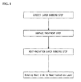
- FIG. 1 A flow chart thereof is shown in FIG. 1 .
- the circuit layer 12 is bonded on the circuit-layer surface of the ceramic substrate 11 at first (a circuit layer bonding step), and then the heat-radiation layer 13 is bonded on the heat-radiation layer surface of the ceramic substrate 11 (a heat-radiation layer bonding step).
- a surface treatment is performed on the surface (the heat-radiation layer surface) of the ceramic substrate 11 on which the the circuit layer 12 is not bonded (a surface treatment step).
- the heat sink 30 is bonded on the heat-radiation layer 13.
- the circuit layer 12 is laminated on the one surface (the circuit-layer surface) of the ceramic substrate 11 with the paste-like or foil-like reactive-metal brazing-material therebetween, so that one of stack bodies 40 is formed.
- the stack bodies 40 are piled with plate-like cushion sheets 50 (made of carbon graphite or the like) therebetween, and pressurized by a pressurizing device 110 as shown in FIG. 3 in a stacking direction with 0.3 MPa to 1.0 MPa for example.
- the pressurizing device 110 includes a base plate 111, guide posts 112 vertically installed at four corners of the base plate 111 on an upper surface, a fixed plate 113 fixed on upper ends of the guide posts 112, a pressurizing plate 114 upward and downward movably held by the guide posts 112 between the base plate 111 and the fixed plate 113, and a pressing means 115 such as a spring or the like provided between the fixed plate 113 and the pressurizing plate 114 so as to press the pressurizing plate 114 downward.
- the above mentioned stack bodies 40 and the cushion sheets 50 are arranged between the base plate 111 and the pressurizing plate 114.
- the stack bodies 40 are heated together with the pressurizing device 110 arranged in a heating furnace (not illustrated) in vacuum atmosphere, at temperature of 800°C or higher and 930°C or lower, for 1 minute to 60 minutes: so that the ceramic substrate 11 and the circuit layer 12 are brazed.
- This brazing is a bonding process using the reactive-metal brazing-material.
- Ti in the brazing material which is the reactive metal, is preferentially spread to the ceramic substrate 11 and forms a Ti compound: so that the circuit layer 12 and the ceramic substrate 11 are bonded with Ag-Cu alloy.
- the oxide film is reduced.
- acid for cleansing one or more selected from hydrochloric acid, nitric acid, and sulfuric acid is used.
- hydrochloric acid is desirable since an oxidative effect is weak; 18% by mass of hydrochloric acid is used, for example.
- the ceramic substrate 11 to which the circuit layer 12 is bonded is drawn up, and cleansed by distilled water in order to remove acid on the surface. And then, furthermore, after being soaked in alcohols, the ceramic substrate 11 with the circuit layer 12 is dried.
- the alcohols ethanol can be used for example.
- nitric acid used for this surface treatment
- the thickness of the oxide film on the heat-radiation layer surface of the ceramic substrate 11 is reduced to 3.2 nm or less at least at a peripheral part of an intended bonding area of the ceramic substrate 11 and the heat-radiation layer 13.
- an outer peripheral part of a bonding interface between the ceramic substrate 11 and the circuit layer 12 is eroded away: accordingly, it is important to reduce the thickness of the oxide film to be less than a prescribed value at the outer peripheral part of the bonding interface.
- the peripheral part in which the thickness of the oxide film to be regulated is at a position of, for example, 1 mm from a peripheral edge of the intended bonding area between the ceramic substrate 11 and the circuit layer 12.
- the thickness of the oxide film can be measured from an analysis result of a surface state by an X-ray photoelectron spectroscopy (XPS) or the like.
- the heat-radiation layer 13 is laminated on the heat-radiation layer surface of the ceramic substrate 11 with brazing material therebetween so as to form a laminate body; a plurality of the stack bodies 40 are piled between the cushion sheets 50 and pressed in a laminating direction by the pressurizing device 110 in, for example, 0.3 MPa to 1.0 MPa (not illustrated).
- the stack bodies 40 are arranged in the heating furnace (not illustrated) together with the pressurizing device 110 in a state of being pressed in the pressurizing device 110, and heated in vacuum atmosphere at temperature of 630°C or higher and 650°C or lower for 1 minute to 60 minutes; so that the ceramic substrates 11 and the heat-radiation layers 13 are brazed, and the power-module substrates 10 are manufactured.
- the oxide film which is generated on the surface of the ceramic substrate 11 while the circuit layer bonding step is reduced by the surface treatment step, and then the heat-radiation layer bonding step is performed. Therefore, the oxide film at the bonding interface between the ceramic substrate 11 and the heat-radiation layer 13 is extremely reduced; and a bonding reliability can be improved at the bonding interface between the ceramic substrate 11 and the heat-radiation layer 13.
- the thickness of the oxide film be reduced on the entire surface of the ceramic substrate 11 in the surface treatment step, since there is the possibility that the separation is occurred at the outer peripheral part in which heat stress is largest among the bonded interface of the ceramic substrate 11 and the heat-radiation layer 13, it is adequate that at least at the outer peripheral part of the intended bonding area of the ceramic substrate 11 and the heat-radiation layer 13, the thickness of the oxide film be reduced to 3.2 nm or less.
- the thicknesses of the oxide films were measured by an XPS analysis.
- X-ray Source Standard AlK ⁇ 350 W Pass Energy: 187.85 eV (Survey), 58.5 eV (Depth) Measuring Interval: 0.8 eV/step (Survey), 0.125 eV (Depth) Take-off Angle of Photoelectron to a surface of the sample: 45 deg Analysis Area: about 800 ⁇ m in diameter Sputter Rate: 1.6 nm/min
- a range in which oxygen-peak area measured by the XPS analysis was a half of an initial value was supposed to be the oxide film; and a thickness of the oxide film was calculated from a sputtering time and the sputter rate.
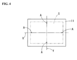
- a thickness of the oxide film was measured at four point of marks A on an X-axis and a Y-axis passing through a center of an intended bonding area S and of 1 mm inside from a peripheral edge of the intended bonding area S of the heat-radiation layer 13 (a 4N-aluminum plate) to the ceramic substrate 11; and an average thereof was the thickness of the oxide film in the samples "a" to "g” (refer to Table 1).
- a 4N-aluminum plate simulating the heat-radiation layer 13 was bonded to the surface of the ceramic substrate using Al-Si based brazing material.
- an aluminum-alloy plate simulating the heat sink 30 is brazed using flux; and the bondability between the ceramic substrate and the 4N-aluminum plate was evaluated in the samples "b" to "g".
- the intended bonding size was a size of the intended bonding area S, i.e., the size of the aluminum plate.
- TABLE 1 shows the evaluation result of the bondability. (TABLE 1) a b c d e f g THICKNESS OF OXIDE FILM 2.1 3.8 3 2.9 2.9 3.2 2.4 BONDABILITY - POOR GOOD GOOD GOOD GOOD GOOD GOOD
Landscapes
- Engineering & Computer Science (AREA)
- Chemical & Material Sciences (AREA)
- Ceramic Engineering (AREA)
- Materials Engineering (AREA)
- Mechanical Engineering (AREA)
- Structural Engineering (AREA)
- Organic Chemistry (AREA)
- Manufacturing & Machinery (AREA)
- Microelectronics & Electronic Packaging (AREA)
- Cooling Or The Like Of Semiconductors Or Solid State Devices (AREA)
Applications Claiming Priority (2)
| Application Number | Priority Date | Filing Date | Title |
|---|---|---|---|
| JP2012275157A JP6056446B2 (ja) | 2012-12-17 | 2012-12-17 | パワーモジュール用基板の製造方法 |
| PCT/JP2013/082449 WO2014097880A1 (ja) | 2012-12-17 | 2013-12-03 | パワーモジュール用基板の製造方法 |
Publications (2)
| Publication Number | Publication Date |
|---|---|
| EP2933831A1 true EP2933831A1 (de) | 2015-10-21 |
| EP2933831A4 EP2933831A4 (de) | 2016-05-25 |
Family
ID=50978215
Family Applications (1)
| Application Number | Title | Priority Date | Filing Date |
|---|---|---|---|
| EP13865283.9A Withdrawn EP2933831A4 (de) | 2012-12-17 | 2013-12-03 | Verfahren zur herstellung eines substrats für leistungsmodule |
Country Status (7)
| Country | Link |
|---|---|
| US (1) | US10057993B2 (de) |
| EP (1) | EP2933831A4 (de) |
| JP (1) | JP6056446B2 (de) |
| KR (1) | KR102198657B1 (de) |
| CN (1) | CN104813466B (de) |
| TW (1) | TWI598929B (de) |
| WO (1) | WO2014097880A1 (de) |
Families Citing this family (3)
| Publication number | Priority date | Publication date | Assignee | Title |
|---|---|---|---|---|
| CN109534842B (zh) * | 2018-11-26 | 2021-08-10 | 北京卫星制造厂有限公司 | 功率半导体模块用焊接工艺 |
| KR102335531B1 (ko) * | 2019-05-17 | 2021-12-07 | 주식회사 아모센스 | 세라믹 기판 제조 방법 |
| CN118123171A (zh) * | 2024-03-21 | 2024-06-04 | 保定中创燕园半导体科技有限公司 | 一种AlN陶瓷基板覆铜自适应钎焊装夹工装 |
Family Cites Families (15)
| Publication number | Priority date | Publication date | Assignee | Title |
|---|---|---|---|---|
| JPS59150453A (ja) * | 1982-12-23 | 1984-08-28 | Toshiba Corp | 半導体モジユ−ル用基板の製造方法 |
| JPH0733293B2 (ja) * | 1990-10-19 | 1995-04-12 | 日本碍子株式会社 | ナトリウム―硫黄電池のセラミックス製絶縁体と金属部品との接合方法 |
| JPH05275559A (ja) * | 1992-03-26 | 1993-10-22 | Mitsubishi Materials Corp | パワーモジュール用セラミックス回路基板の製造方法 |
| MY139405A (en) * | 1998-09-28 | 2009-09-30 | Ibiden Co Ltd | Printed circuit board and method for its production |
| JP2001135902A (ja) * | 1999-11-10 | 2001-05-18 | Denki Kagaku Kogyo Kk | セラミックス回路基板 |
| JP5038565B2 (ja) * | 2000-09-22 | 2012-10-03 | 株式会社東芝 | セラミックス回路基板およびその製造方法 |
| JP2003007939A (ja) * | 2001-06-19 | 2003-01-10 | Mitsubishi Materials Corp | ヒートシンク付セラミック回路基板及びその製造方法 |
| JP2003197826A (ja) * | 2001-12-26 | 2003-07-11 | Toshiba Corp | セラミックス回路基板およびそれを用いた半導体モジュール |
| JP3935037B2 (ja) * | 2002-09-30 | 2007-06-20 | Dowaホールディングス株式会社 | アルミニウム−セラミックス接合基板の製造方法 |
| US20040149689A1 (en) * | 2002-12-03 | 2004-08-05 | Xiao-Shan Ning | Method for producing metal/ceramic bonding substrate |
| CN101849445B (zh) * | 2007-11-06 | 2012-11-21 | 三菱综合材料株式会社 | 陶瓷基板、陶瓷基板的制造方法和电源模块用基板的制造方法 |
| US8609993B2 (en) * | 2008-05-16 | 2013-12-17 | Mitsubishi Materials Corporation | Power module substrate, power module, and method for manufacturing power module substrate |
| CN102047413B (zh) * | 2008-06-06 | 2015-04-15 | 三菱综合材料株式会社 | 功率模块用基板、功率模块以及功率模块用基板的制造方法 |
| JP5245989B2 (ja) * | 2009-03-31 | 2013-07-24 | 三菱マテリアル株式会社 | パワーモジュール用基板の製造方法およびヒートシンク付パワーモジュール用基板の製造方法 |
| DE102011103746A1 (de) * | 2011-05-31 | 2012-12-06 | Ixys Semiconductor Gmbh | Verfahren zum Fügen von Metall-Keramik-Substraten an Metallkörpern |
-
2012
- 2012-12-17 JP JP2012275157A patent/JP6056446B2/ja not_active Expired - Fee Related
-
2013
- 2013-12-03 KR KR1020157018455A patent/KR102198657B1/ko active Active
- 2013-12-03 WO PCT/JP2013/082449 patent/WO2014097880A1/ja not_active Ceased
- 2013-12-03 CN CN201380061034.5A patent/CN104813466B/zh not_active Expired - Fee Related
- 2013-12-03 US US14/652,554 patent/US10057993B2/en active Active
- 2013-12-03 EP EP13865283.9A patent/EP2933831A4/de not_active Withdrawn
- 2013-12-09 TW TW102145131A patent/TWI598929B/zh active
Also Published As
| Publication number | Publication date |
|---|---|
| US10057993B2 (en) | 2018-08-21 |
| TW201435970A (zh) | 2014-09-16 |
| TWI598929B (zh) | 2017-09-11 |
| JP2014120634A (ja) | 2014-06-30 |
| KR102198657B1 (ko) | 2021-01-05 |
| JP6056446B2 (ja) | 2017-01-11 |
| KR20150097597A (ko) | 2015-08-26 |
| WO2014097880A1 (ja) | 2014-06-26 |
| CN104813466A (zh) | 2015-07-29 |
| EP2933831A4 (de) | 2016-05-25 |
| CN104813466B (zh) | 2017-12-15 |
| US20150289385A1 (en) | 2015-10-08 |
Similar Documents
| Publication | Publication Date | Title |
|---|---|---|
| EP2911192B1 (de) | Substrat für ein strommodul mit einem kühlkörper, strommodul mit einem kühlkörper und verfahren zur herstellung des substrats für das strommodul mit einem kühlkörper | |
| US9357643B2 (en) | Ceramic/copper circuit board and semiconductor device | |
| US9560755B2 (en) | Bonding body, power module substrate, and heat-sink-attached power module substrate | |
| EP2080224B1 (de) | Leistungsmodulsubstrat und leistungsmodul | |
| JP6499545B2 (ja) | 金属セラミック接合基板及び、その製造方法 | |
| CN102027592B (zh) | 功率模块用基板、功率模块及功率模块用基板的制造方法 | |
| EP3196928A1 (de) | Verfahren zur herstellung eines substrats für leistungsmodule | |
| JP5786569B2 (ja) | パワーモジュール用基板の製造方法 | |
| CN103390562A (zh) | 冷却器的制造方法 | |
| EP2933831A1 (de) | Verfahren zur herstellung eines substrats für leistungsmodule | |
| EP3761351B1 (de) | Isolierte leiterplatte | |
| EP3761764A1 (de) | Isolierende leiterplatte | |
| JP6152626B2 (ja) | パワーモジュール用基板の製造方法 | |
| KR101929613B1 (ko) | 세라믹 회로기판 및 이의 제조방법 | |
| JP6079345B2 (ja) | パワーモジュール用基板およびその製造方法 | |
| JP6422294B2 (ja) | 電子モジュール用基板の製造方法及び電子モジュール用基板 | |
| JP2003282770A (ja) | 金属ベース板付き回路基板及びモジュール | |
| EP4378914A1 (de) | Kupfer/keramik verbundkörper und isolierte leiterplatte | |
| US11887909B2 (en) | Copper/titanium/aluminum joint, insulating circuit substrate, insulating circuit substrate with heat sink, power module, LED module, and thermoelectric module | |
| WO2022202144A1 (ja) | 複合基板 | |
| WO2023204054A1 (ja) | セラミックス回路基板、半導体装置、セラミックス回路基板の製造方法、及び半導体装置の製造方法 | |
| CN118742527A (zh) | 铜-陶瓷接合基板及其制造方法 |
Legal Events
| Date | Code | Title | Description |
|---|---|---|---|
| PUAI | Public reference made under article 153(3) epc to a published international application that has entered the european phase |
Free format text: ORIGINAL CODE: 0009012 |
|
| 17P | Request for examination filed |
Effective date: 20150629 |
|
| AK | Designated contracting states |
Kind code of ref document: A1 Designated state(s): AL AT BE BG CH CY CZ DE DK EE ES FI FR GB GR HR HU IE IS IT LI LT LU LV MC MK MT NL NO PL PT RO RS SE SI SK SM TR |
|
| AX | Request for extension of the european patent |
Extension state: BA ME |
|
| DAX | Request for extension of the european patent (deleted) | ||
| A4 | Supplementary search report drawn up and despatched |
Effective date: 20160425 |
|
| RIC1 | Information provided on ipc code assigned before grant |
Ipc: H01L 23/36 20060101ALI20160419BHEP Ipc: H01L 23/12 20060101AFI20160419BHEP Ipc: C04B 37/02 20060101ALI20160419BHEP |
|
| STAA | Information on the status of an ep patent application or granted ep patent |
Free format text: STATUS: EXAMINATION IS IN PROGRESS |
|
| 17Q | First examination report despatched |
Effective date: 20190506 |
|
| STAA | Information on the status of an ep patent application or granted ep patent |
Free format text: STATUS: THE APPLICATION HAS BEEN WITHDRAWN |
|
| RAP1 | Party data changed (applicant data changed or rights of an application transferred) |
Owner name: MITSUBISHI MATERIALS CORPORATION |
|
| 18W | Application withdrawn |
Effective date: 20190710 |